US9536188B2 - Dual-interface IC card components and method for manufacturing the dual-interface IC card components - Google Patents
Dual-interface IC card components and method for manufacturing the dual-interface IC card components Download PDFInfo
- Publication number
- US9536188B2 US9536188B2 US14/677,836 US201514677836A US9536188B2 US 9536188 B2 US9536188 B2 US 9536188B2 US 201514677836 A US201514677836 A US 201514677836A US 9536188 B2 US9536188 B2 US 9536188B2
- Authority
- US
- United States
- Prior art keywords
- contact
- dual
- interface
- antenna
- substrate
- Prior art date
- Legal status (The legal status is an assumption and is not a legal conclusion. Google has not performed a legal analysis and makes no representation as to the accuracy of the status listed.)
- Active
Links
Images


Classifications
-
- G—PHYSICS
- G06—COMPUTING; CALCULATING OR COUNTING
- G06K—GRAPHICAL DATA READING; PRESENTATION OF DATA; RECORD CARRIERS; HANDLING RECORD CARRIERS
- G06K19/00—Record carriers for use with machines and with at least a part designed to carry digital markings
- G06K19/06—Record carriers for use with machines and with at least a part designed to carry digital markings characterised by the kind of the digital marking, e.g. shape, nature, code
- G06K19/067—Record carriers with conductive marks, printed circuits or semiconductor circuit elements, e.g. credit or identity cards also with resonating or responding marks without active components
- G06K19/07—Record carriers with conductive marks, printed circuits or semiconductor circuit elements, e.g. credit or identity cards also with resonating or responding marks without active components with integrated circuit chips
- G06K19/077—Constructional details, e.g. mounting of circuits in the carrier
- G06K19/07749—Constructional details, e.g. mounting of circuits in the carrier the record carrier being capable of non-contact communication, e.g. constructional details of the antenna of a non-contact smart card
- G06K19/07766—Constructional details, e.g. mounting of circuits in the carrier the record carrier being capable of non-contact communication, e.g. constructional details of the antenna of a non-contact smart card comprising at least a second communication arrangement in addition to a first non-contact communication arrangement
- G06K19/07769—Constructional details, e.g. mounting of circuits in the carrier the record carrier being capable of non-contact communication, e.g. constructional details of the antenna of a non-contact smart card comprising at least a second communication arrangement in addition to a first non-contact communication arrangement the further communication means being a galvanic interface, e.g. hybrid or mixed smart cards having a contact and a non-contact interface
-
- G—PHYSICS
- G06—COMPUTING; CALCULATING OR COUNTING
- G06K—GRAPHICAL DATA READING; PRESENTATION OF DATA; RECORD CARRIERS; HANDLING RECORD CARRIERS
- G06K19/00—Record carriers for use with machines and with at least a part designed to carry digital markings
- G06K19/06—Record carriers for use with machines and with at least a part designed to carry digital markings characterised by the kind of the digital marking, e.g. shape, nature, code
- G06K19/067—Record carriers with conductive marks, printed circuits or semiconductor circuit elements, e.g. credit or identity cards also with resonating or responding marks without active components
- G06K19/07—Record carriers with conductive marks, printed circuits or semiconductor circuit elements, e.g. credit or identity cards also with resonating or responding marks without active components with integrated circuit chips
- G06K19/077—Constructional details, e.g. mounting of circuits in the carrier
- G06K19/07745—Mounting details of integrated circuit chips
- G06K19/07747—Mounting details of integrated circuit chips at least one of the integrated circuit chips being mounted as a module
-
- G—PHYSICS
- G06—COMPUTING; CALCULATING OR COUNTING
- G06K—GRAPHICAL DATA READING; PRESENTATION OF DATA; RECORD CARRIERS; HANDLING RECORD CARRIERS
- G06K19/00—Record carriers for use with machines and with at least a part designed to carry digital markings
- G06K19/06—Record carriers for use with machines and with at least a part designed to carry digital markings characterised by the kind of the digital marking, e.g. shape, nature, code
- G06K19/067—Record carriers with conductive marks, printed circuits or semiconductor circuit elements, e.g. credit or identity cards also with resonating or responding marks without active components
- G06K19/07—Record carriers with conductive marks, printed circuits or semiconductor circuit elements, e.g. credit or identity cards also with resonating or responding marks without active components with integrated circuit chips
- G06K19/077—Constructional details, e.g. mounting of circuits in the carrier
- G06K19/07749—Constructional details, e.g. mounting of circuits in the carrier the record carrier being capable of non-contact communication, e.g. constructional details of the antenna of a non-contact smart card
- G06K19/0775—Constructional details, e.g. mounting of circuits in the carrier the record carrier being capable of non-contact communication, e.g. constructional details of the antenna of a non-contact smart card arrangements for connecting the integrated circuit to the antenna
- G06K19/07754—Constructional details, e.g. mounting of circuits in the carrier the record carrier being capable of non-contact communication, e.g. constructional details of the antenna of a non-contact smart card arrangements for connecting the integrated circuit to the antenna the connection being galvanic
-
- H—ELECTRICITY
- H01—ELECTRIC ELEMENTS
- H01L—SEMICONDUCTOR DEVICES NOT COVERED BY CLASS H10
- H01L23/00—Details of semiconductor or other solid state devices
- H01L23/48—Arrangements for conducting electric current to or from the solid state body in operation, e.g. leads, terminal arrangements ; Selection of materials therefor
- H01L23/488—Arrangements for conducting electric current to or from the solid state body in operation, e.g. leads, terminal arrangements ; Selection of materials therefor consisting of soldered or bonded constructions
- H01L23/498—Leads, i.e. metallisations or lead-frames on insulating substrates, e.g. chip carriers
- H01L23/49855—Leads, i.e. metallisations or lead-frames on insulating substrates, e.g. chip carriers for flat-cards, e.g. credit cards
-
- H—ELECTRICITY
- H01—ELECTRIC ELEMENTS
- H01L—SEMICONDUCTOR DEVICES NOT COVERED BY CLASS H10
- H01L24/00—Arrangements for connecting or disconnecting semiconductor or solid-state bodies; Methods or apparatus related thereto
- H01L24/01—Means for bonding being attached to, or being formed on, the surface to be connected, e.g. chip-to-package, die-attach, "first-level" interconnects; Manufacturing methods related thereto
- H01L24/42—Wire connectors; Manufacturing methods related thereto
- H01L24/47—Structure, shape, material or disposition of the wire connectors after the connecting process
- H01L24/49—Structure, shape, material or disposition of the wire connectors after the connecting process of a plurality of wire connectors
-
- H—ELECTRICITY
- H01—ELECTRIC ELEMENTS
- H01L—SEMICONDUCTOR DEVICES NOT COVERED BY CLASS H10
- H01L24/00—Arrangements for connecting or disconnecting semiconductor or solid-state bodies; Methods or apparatus related thereto
- H01L24/80—Methods for connecting semiconductor or other solid state bodies using means for bonding being attached to, or being formed on, the surface to be connected
- H01L24/83—Methods for connecting semiconductor or other solid state bodies using means for bonding being attached to, or being formed on, the surface to be connected using a layer connector
-
- H—ELECTRICITY
- H01—ELECTRIC ELEMENTS
- H01L—SEMICONDUCTOR DEVICES NOT COVERED BY CLASS H10
- H01L24/00—Arrangements for connecting or disconnecting semiconductor or solid-state bodies; Methods or apparatus related thereto
- H01L24/93—Batch processes
- H01L24/95—Batch processes at chip-level, i.e. with connecting carried out on a plurality of singulated devices, i.e. on diced chips
- H01L24/97—Batch processes at chip-level, i.e. with connecting carried out on a plurality of singulated devices, i.e. on diced chips the devices being connected to a common substrate, e.g. interposer, said common substrate being separable into individual assemblies after connecting
-
- H—ELECTRICITY
- H01—ELECTRIC ELEMENTS
- H01L—SEMICONDUCTOR DEVICES NOT COVERED BY CLASS H10
- H01L2224/00—Indexing scheme for arrangements for connecting or disconnecting semiconductor or solid-state bodies and methods related thereto as covered by H01L24/00
- H01L2224/01—Means for bonding being attached to, or being formed on, the surface to be connected, e.g. chip-to-package, die-attach, "first-level" interconnects; Manufacturing methods related thereto
- H01L2224/26—Layer connectors, e.g. plate connectors, solder or adhesive layers; Manufacturing methods related thereto
- H01L2224/31—Structure, shape, material or disposition of the layer connectors after the connecting process
- H01L2224/32—Structure, shape, material or disposition of the layer connectors after the connecting process of an individual layer connector
- H01L2224/321—Disposition
- H01L2224/32151—Disposition the layer connector connecting between a semiconductor or solid-state body and an item not being a semiconductor or solid-state body, e.g. chip-to-substrate, chip-to-passive
- H01L2224/32221—Disposition the layer connector connecting between a semiconductor or solid-state body and an item not being a semiconductor or solid-state body, e.g. chip-to-substrate, chip-to-passive the body and the item being stacked
- H01L2224/32225—Disposition the layer connector connecting between a semiconductor or solid-state body and an item not being a semiconductor or solid-state body, e.g. chip-to-substrate, chip-to-passive the body and the item being stacked the item being non-metallic, e.g. insulating substrate with or without metallisation
-
- H—ELECTRICITY
- H01—ELECTRIC ELEMENTS
- H01L—SEMICONDUCTOR DEVICES NOT COVERED BY CLASS H10
- H01L2224/00—Indexing scheme for arrangements for connecting or disconnecting semiconductor or solid-state bodies and methods related thereto as covered by H01L24/00
- H01L2224/01—Means for bonding being attached to, or being formed on, the surface to be connected, e.g. chip-to-package, die-attach, "first-level" interconnects; Manufacturing methods related thereto
- H01L2224/42—Wire connectors; Manufacturing methods related thereto
- H01L2224/44—Structure, shape, material or disposition of the wire connectors prior to the connecting process
- H01L2224/45—Structure, shape, material or disposition of the wire connectors prior to the connecting process of an individual wire connector
- H01L2224/45001—Core members of the connector
- H01L2224/45099—Material
- H01L2224/451—Material with a principal constituent of the material being a metal or a metalloid, e.g. boron (B), silicon (Si), germanium (Ge), arsenic (As), antimony (Sb), tellurium (Te) and polonium (Po), and alloys thereof
- H01L2224/45117—Material with a principal constituent of the material being a metal or a metalloid, e.g. boron (B), silicon (Si), germanium (Ge), arsenic (As), antimony (Sb), tellurium (Te) and polonium (Po), and alloys thereof the principal constituent melting at a temperature of greater than or equal to 400°C and less than 950°C
- H01L2224/45124—Aluminium (Al) as principal constituent
-
- H—ELECTRICITY
- H01—ELECTRIC ELEMENTS
- H01L—SEMICONDUCTOR DEVICES NOT COVERED BY CLASS H10
- H01L2224/00—Indexing scheme for arrangements for connecting or disconnecting semiconductor or solid-state bodies and methods related thereto as covered by H01L24/00
- H01L2224/01—Means for bonding being attached to, or being formed on, the surface to be connected, e.g. chip-to-package, die-attach, "first-level" interconnects; Manufacturing methods related thereto
- H01L2224/42—Wire connectors; Manufacturing methods related thereto
- H01L2224/44—Structure, shape, material or disposition of the wire connectors prior to the connecting process
- H01L2224/45—Structure, shape, material or disposition of the wire connectors prior to the connecting process of an individual wire connector
- H01L2224/45001—Core members of the connector
- H01L2224/45099—Material
- H01L2224/451—Material with a principal constituent of the material being a metal or a metalloid, e.g. boron (B), silicon (Si), germanium (Ge), arsenic (As), antimony (Sb), tellurium (Te) and polonium (Po), and alloys thereof
- H01L2224/45138—Material with a principal constituent of the material being a metal or a metalloid, e.g. boron (B), silicon (Si), germanium (Ge), arsenic (As), antimony (Sb), tellurium (Te) and polonium (Po), and alloys thereof the principal constituent melting at a temperature of greater than or equal to 950°C and less than 1550°C
- H01L2224/45147—Copper (Cu) as principal constituent
-
- H—ELECTRICITY
- H01—ELECTRIC ELEMENTS
- H01L—SEMICONDUCTOR DEVICES NOT COVERED BY CLASS H10
- H01L2224/00—Indexing scheme for arrangements for connecting or disconnecting semiconductor or solid-state bodies and methods related thereto as covered by H01L24/00
- H01L2224/01—Means for bonding being attached to, or being formed on, the surface to be connected, e.g. chip-to-package, die-attach, "first-level" interconnects; Manufacturing methods related thereto
- H01L2224/42—Wire connectors; Manufacturing methods related thereto
- H01L2224/47—Structure, shape, material or disposition of the wire connectors after the connecting process
- H01L2224/48—Structure, shape, material or disposition of the wire connectors after the connecting process of an individual wire connector
- H01L2224/4805—Shape
- H01L2224/4809—Loop shape
- H01L2224/48091—Arched
-
- H—ELECTRICITY
- H01—ELECTRIC ELEMENTS
- H01L—SEMICONDUCTOR DEVICES NOT COVERED BY CLASS H10
- H01L2224/00—Indexing scheme for arrangements for connecting or disconnecting semiconductor or solid-state bodies and methods related thereto as covered by H01L24/00
- H01L2224/01—Means for bonding being attached to, or being formed on, the surface to be connected, e.g. chip-to-package, die-attach, "first-level" interconnects; Manufacturing methods related thereto
- H01L2224/42—Wire connectors; Manufacturing methods related thereto
- H01L2224/47—Structure, shape, material or disposition of the wire connectors after the connecting process
- H01L2224/48—Structure, shape, material or disposition of the wire connectors after the connecting process of an individual wire connector
- H01L2224/481—Disposition
- H01L2224/48151—Connecting between a semiconductor or solid-state body and an item not being a semiconductor or solid-state body, e.g. chip-to-substrate, chip-to-passive
- H01L2224/48221—Connecting between a semiconductor or solid-state body and an item not being a semiconductor or solid-state body, e.g. chip-to-substrate, chip-to-passive the body and the item being stacked
- H01L2224/48225—Connecting between a semiconductor or solid-state body and an item not being a semiconductor or solid-state body, e.g. chip-to-substrate, chip-to-passive the body and the item being stacked the item being non-metallic, e.g. insulating substrate with or without metallisation
- H01L2224/48227—Connecting between a semiconductor or solid-state body and an item not being a semiconductor or solid-state body, e.g. chip-to-substrate, chip-to-passive the body and the item being stacked the item being non-metallic, e.g. insulating substrate with or without metallisation connecting the wire to a bond pad of the item
- H01L2224/48228—Connecting between a semiconductor or solid-state body and an item not being a semiconductor or solid-state body, e.g. chip-to-substrate, chip-to-passive the body and the item being stacked the item being non-metallic, e.g. insulating substrate with or without metallisation connecting the wire to a bond pad of the item the bond pad being disposed in a recess of the surface of the item
-
- H—ELECTRICITY
- H01—ELECTRIC ELEMENTS
- H01L—SEMICONDUCTOR DEVICES NOT COVERED BY CLASS H10
- H01L2224/00—Indexing scheme for arrangements for connecting or disconnecting semiconductor or solid-state bodies and methods related thereto as covered by H01L24/00
- H01L2224/01—Means for bonding being attached to, or being formed on, the surface to be connected, e.g. chip-to-package, die-attach, "first-level" interconnects; Manufacturing methods related thereto
- H01L2224/42—Wire connectors; Manufacturing methods related thereto
- H01L2224/47—Structure, shape, material or disposition of the wire connectors after the connecting process
- H01L2224/48—Structure, shape, material or disposition of the wire connectors after the connecting process of an individual wire connector
- H01L2224/484—Connecting portions
- H01L2224/48463—Connecting portions the connecting portion on the bonding area of the semiconductor or solid-state body being a ball bond
- H01L2224/48465—Connecting portions the connecting portion on the bonding area of the semiconductor or solid-state body being a ball bond the other connecting portion not on the bonding area being a wedge bond, i.e. ball-to-wedge, regular stitch
-
- H—ELECTRICITY
- H01—ELECTRIC ELEMENTS
- H01L—SEMICONDUCTOR DEVICES NOT COVERED BY CLASS H10
- H01L2224/00—Indexing scheme for arrangements for connecting or disconnecting semiconductor or solid-state bodies and methods related thereto as covered by H01L24/00
- H01L2224/01—Means for bonding being attached to, or being formed on, the surface to be connected, e.g. chip-to-package, die-attach, "first-level" interconnects; Manufacturing methods related thereto
- H01L2224/42—Wire connectors; Manufacturing methods related thereto
- H01L2224/47—Structure, shape, material or disposition of the wire connectors after the connecting process
- H01L2224/49—Structure, shape, material or disposition of the wire connectors after the connecting process of a plurality of wire connectors
- H01L2224/491—Disposition
- H01L2224/49105—Connecting at different heights
- H01L2224/49109—Connecting at different heights outside the semiconductor or solid-state body
-
- H—ELECTRICITY
- H01—ELECTRIC ELEMENTS
- H01L—SEMICONDUCTOR DEVICES NOT COVERED BY CLASS H10
- H01L2224/00—Indexing scheme for arrangements for connecting or disconnecting semiconductor or solid-state bodies and methods related thereto as covered by H01L24/00
- H01L2224/01—Means for bonding being attached to, or being formed on, the surface to be connected, e.g. chip-to-package, die-attach, "first-level" interconnects; Manufacturing methods related thereto
- H01L2224/42—Wire connectors; Manufacturing methods related thereto
- H01L2224/47—Structure, shape, material or disposition of the wire connectors after the connecting process
- H01L2224/49—Structure, shape, material or disposition of the wire connectors after the connecting process of a plurality of wire connectors
- H01L2224/491—Disposition
- H01L2224/4912—Layout
- H01L2224/49171—Fan-out arrangements
-
- H—ELECTRICITY
- H01—ELECTRIC ELEMENTS
- H01L—SEMICONDUCTOR DEVICES NOT COVERED BY CLASS H10
- H01L2224/00—Indexing scheme for arrangements for connecting or disconnecting semiconductor or solid-state bodies and methods related thereto as covered by H01L24/00
- H01L2224/73—Means for bonding being of different types provided for in two or more of groups H01L2224/10, H01L2224/18, H01L2224/26, H01L2224/34, H01L2224/42, H01L2224/50, H01L2224/63, H01L2224/71
- H01L2224/732—Location after the connecting process
- H01L2224/73251—Location after the connecting process on different surfaces
- H01L2224/73265—Layer and wire connectors
-
- H—ELECTRICITY
- H01—ELECTRIC ELEMENTS
- H01L—SEMICONDUCTOR DEVICES NOT COVERED BY CLASS H10
- H01L2224/00—Indexing scheme for arrangements for connecting or disconnecting semiconductor or solid-state bodies and methods related thereto as covered by H01L24/00
- H01L2224/80—Methods for connecting semiconductor or other solid state bodies using means for bonding being attached to, or being formed on, the surface to be connected
- H01L2224/85—Methods for connecting semiconductor or other solid state bodies using means for bonding being attached to, or being formed on, the surface to be connected using a wire connector
- H01L2224/85909—Post-treatment of the connector or wire bonding area
- H01L2224/8592—Applying permanent coating, e.g. protective coating
-
- H—ELECTRICITY
- H01—ELECTRIC ELEMENTS
- H01L—SEMICONDUCTOR DEVICES NOT COVERED BY CLASS H10
- H01L24/00—Arrangements for connecting or disconnecting semiconductor or solid-state bodies; Methods or apparatus related thereto
- H01L24/01—Means for bonding being attached to, or being formed on, the surface to be connected, e.g. chip-to-package, die-attach, "first-level" interconnects; Manufacturing methods related thereto
- H01L24/42—Wire connectors; Manufacturing methods related thereto
- H01L24/44—Structure, shape, material or disposition of the wire connectors prior to the connecting process
- H01L24/45—Structure, shape, material or disposition of the wire connectors prior to the connecting process of an individual wire connector
-
- H—ELECTRICITY
- H01—ELECTRIC ELEMENTS
- H01L—SEMICONDUCTOR DEVICES NOT COVERED BY CLASS H10
- H01L24/00—Arrangements for connecting or disconnecting semiconductor or solid-state bodies; Methods or apparatus related thereto
- H01L24/01—Means for bonding being attached to, or being formed on, the surface to be connected, e.g. chip-to-package, die-attach, "first-level" interconnects; Manufacturing methods related thereto
- H01L24/42—Wire connectors; Manufacturing methods related thereto
- H01L24/47—Structure, shape, material or disposition of the wire connectors after the connecting process
- H01L24/48—Structure, shape, material or disposition of the wire connectors after the connecting process of an individual wire connector
-
- H—ELECTRICITY
- H01—ELECTRIC ELEMENTS
- H01L—SEMICONDUCTOR DEVICES NOT COVERED BY CLASS H10
- H01L2924/00—Indexing scheme for arrangements or methods for connecting or disconnecting semiconductor or solid-state bodies as covered by H01L24/00
-
- H—ELECTRICITY
- H01—ELECTRIC ELEMENTS
- H01L—SEMICONDUCTOR DEVICES NOT COVERED BY CLASS H10
- H01L2924/00—Indexing scheme for arrangements or methods for connecting or disconnecting semiconductor or solid-state bodies as covered by H01L24/00
- H01L2924/0001—Technical content checked by a classifier
- H01L2924/00014—Technical content checked by a classifier the subject-matter covered by the group, the symbol of which is combined with the symbol of this group, being disclosed without further technical details
-
- H—ELECTRICITY
- H01—ELECTRIC ELEMENTS
- H01L—SEMICONDUCTOR DEVICES NOT COVERED BY CLASS H10
- H01L2924/00—Indexing scheme for arrangements or methods for connecting or disconnecting semiconductor or solid-state bodies as covered by H01L24/00
- H01L2924/013—Alloys
-
- H—ELECTRICITY
- H01—ELECTRIC ELEMENTS
- H01L—SEMICONDUCTOR DEVICES NOT COVERED BY CLASS H10
- H01L2924/00—Indexing scheme for arrangements or methods for connecting or disconnecting semiconductor or solid-state bodies as covered by H01L24/00
- H01L2924/10—Details of semiconductor or other solid state devices to be connected
- H01L2924/11—Device type
- H01L2924/12—Passive devices, e.g. 2 terminal devices
- H01L2924/1204—Optical Diode
- H01L2924/12042—LASER
Definitions
- Embodiments of the invention relate generally to electronic circuits and, more particularly, to integrated circuit (IC) devices and methods for manufacturing IC devices.
- IC integrated circuit
- An IC card such as a smart card, includes an embedded integrated circuit that can be used to store information and perform data processing.
- a portable IC card can be used in financial, transportation, security, healthcare, or other applications to provide identification and authentication.
- Types of IC cards include contact IC cards that communicate via electrical contacts, contactless IC cards that communicate wirelessly through antennas, and dual-interface IC cards that communicate via electrical contacts and wirelessly through antennas.
- contact IC cards and contactless IC cards dual-interface IC cards allow users to switch between contact card readers and contactless card readers.
- dual-interface IC cards include both electrical contacts and antennas, the dual-interface IC cards are more expensive to manufacture than contact IC cards and contactless IC cards.
- a dual-interface IC card is generally required to fulfill mechanical requirements to ensure that the dual-interface IC card can continue to operate properly under mechanical stress.
- the chip card module of a dual-interface IC card needs to continue to be attached to the card body when a mechanical load is applied to the card body.
- the chip card module of a dual-interface IC card needs to deform together with the card body and stay functional after certain mechanical deformation.
- the chip card module needs to protect the integrated circuit and wire connections inside the chip card module of a dual-interface IC card from being damaged by mechanical deformation. Therefore, there is a need for low-cost and flexible dual-interface IC card components and manufacturing flexible dual-interface IC card components in a cost-effective manner.
- a dual-interface IC card component includes a single-sided contact base structure, which includes a substrate with an electrical contact layer. On the single-sided contact base structure, one or more antenna contact leads are attached to the single-sided contact base structure to form a dual-interface contact structure by applying an adhesive material to partially cover an overlapping area of the at least one antenna contact and the substrate, which is a component of a dual-interface IC card.
- the dual-interface contact structure is more cost-effective than using a prefabricated dual-interface contact tape currently available in the marketplace, which is typically made from scratch using etching or stamping technology.
- the dual-interface contact structure is more cost-effective than a dual-interface contact structure manufactured by applying an adhesive material to completely cover an overlapping area of an antenna contact and a substrate.
- Other embodiments are also described.
- a method for manufacturing a dual-interface IC card component involves obtaining a single-sided contact base structure, where the single-sided contact base structure includes a substrate with an electrical contact layer and attaching at least one antenna contact lead to the single-sided contact base structure by applying an adhesive material to partially cover an overlapping area of the at least one antenna contact and the substrate to form a dual-interface contact structure, which is a component of a dual-interface IC card.
- a method for manufacturing a dual-interface IC card component involves obtaining a base structure, where the base structure includes a substrate, attaching at least one antenna contact lead to the base structure by applying an adhesive material to partially cover an overlapping area of the at least one antenna contact and the substrate to form a dual-interface contact structure, which is a component of a dual-interface IC card and plating the at least one antenna contact and the base structure with at least one metal material.
- a dual-interface IC card component includes a substrate, an electrical contact layer attached to a first side of the substrate and at least one antenna contact lead glued to a second, opposite, side of the substrate in an area that is smaller than the overlapping area of the at least one antenna contact and the substrate.
- the electrical contact layer includes a contact plate and a plurality of grooves.
- FIG. 1 is a cross-sectional view of a dual-interface IC card in accordance with an embodiment of the invention.
- FIG. 2 depicts a front-side view of an embodiment of a dual-interface IC chip module of the dual-interface IC card depicted in FIG. 1 .
- FIG. 3 depicts a back-side view of the dual-interface IC chip module depicted in FIG. 2 .
- FIG. 4 depicts an embodiment of a single-sided contact tape, which is used to produce a dual-interface contact base structure for the dual-interface IC chip module depicted in FIG. 2 .
- FIG. 5 is a cross-sectional view of a single-sided contact tape depicted in FIG. 4 .
- FIG. 6 depicts an embodiment of a single-sided contact tape with adhesive material applied to the tape.
- FIG. 7 is a cross-sectional view of the single-sided contact tape depicted in FIG. 6 .
- FIG. 8 depicts an embodiment of a dual-interface contact structure having an antenna contact lead.
- FIG. 9 is a cross-sectional view of the dual-interface contact structure depicted in FIG. 8 .
- FIG. 10 depicts an embodiment of a reel of dual-interface IC chip modules produced using the dual-interface contact structure depicted in FIGS. 8 and 9 .
- FIG. 11 is a cross-sectional view of a single dual-interface IC chip module depicted in FIG. 10 .
- FIG. 12 illustrates some mechanical tests for the dual-interface IC card depicted in FIG. 1 .
- FIG. 13 illustrates a deformation of the dual-interface IC card depicted in FIG. 1 under mechanical tests.
- FIG. 14 is a process flow diagram of a method for manufacturing a dual-interface IC card component in accordance with an embodiment of the invention.
- FIG. 15 is a process flow diagram of a method for manufacturing a dual-interface IC card component in accordance with another embodiment of the invention.
- FIG. 1 is a cross-sectional view of a dual-interface IC card 100 in accordance with an embodiment of the invention.
- the dual-interface IC card can be used in financial, transportation, security, healthcare, or other applications to store information and perform data processing.
- the dual-interface IC card has the ability to securely manage, store and provide access to data on the card, perform on-card functions, such as encryption, authentication, and authorization, and interact intelligently with a card reader.
- the dual-interface IC card can communicate by electrical contacts or wirelessly through an antenna.
- the dual-interface IC card is a smart card, which can be used in Near field communication (NFC) applications.
- NFC Near field communication
- the IC card is a smart card that is designed to be compatible with the International Organization for Standardization (ISO)/the International Electrotechnical Commission (IEC) 14443.
- ISO International Organization for Standardization
- IEC International Electrotechnical Commission
- the manufacturing cost of the dual-interface IC card can be significantly lower than conventional dual-interface IC cards because the dual-interface IC card can be produced using a prefabricated single-sided contact base structure that is used to make a module for a contact smart card (e.g., a standard single-sided contact tape currently available in the marketplace), rather than a more expensive prefabricated double-sided contact base structure that is used to make a module for a dual-interface smart card (e.g., a standard double-sided contact tape currently available in the market).
- the manufacturing cost of the dual-interface IC card can be significantly lower than
- the dual-interface IC card 100 includes a contact layer 102 , a substrate 104 , an adhesive layer 106 , antenna contact leads 108 , an IC chip 110 , bond wires 112 , an encapsulation 114 , adhesives 116 , an electrical connection layer 118 , an antenna layer 120 , and a card body 122 .
- the dual-interface IC card is shown in FIG. 1 as including certain components, in other embodiments, the dual-interface IC card may include fewer components or additional components that are commonly found in conventional dual-interface smart cards.
- the contact layer 102 of the dual-interface IC card 100 is used to make electrical contacts with a card reader to communicate with the card reader.
- the contact layer is located at the front side of the dual-interface IC card while the card body 122 is located at the back side of the dual-interface IC card.
- the contact layer may be made of metal or other conductive material.
- the contact layer is made of Gold (Au)-Nickel (Ni) plated Copper (Cu) foil or galvano deposited Cu.
- the contact layer which is also referred to as the contact pad, provides electrical connectivity when the dual-interface IC card is inserted into a card reader.
- the contact layer is designed and produced to be compatible with the International Organization for Standardization (ISO) 7816.
- the contact layer typically includes groove/recess lines used to electrically insulate contact areas of the contact layer from each other and make the contact layer more flexible.
- the contact layer has two groove lines 124 - 1 , 124 - 2 .
- the contact layer may have any number of groove lines.
- the substrate 104 is used to support other elements of the dual-interface IC card 100 , such as the contact layer 102 , the antenna contact leads 108 and the IC chip 110 .
- the substrate may be made of any suitable substrate material.
- the substrate may be made of Epoxy glass, fiberglass, or plastic substrates (Polyethylene naphthalate (PEN), etc.).
- PEN Polyethylene naphthalate
- a bonding hole 126 is present on the substrate to enable wire bonding of the IC chip 100 to the contact layer.
- the substrate may be in the form of a sheet or a tape.
- the contact layer and the substrate form a single-sided contact base structure, which may be packaged into a single-sided contact tape.
- a device manufacturer may produce a prefabricated single-sided contact base structure that includes the contact layer and the substrate in mass quantities.
- an optional adhesive layer 103 is located between the contact layer and the substrate.
- the adhesive layer 106 of the dual-interface IC card 100 is used to attach the antenna contact leads 108 onto the substrate 104 .
- the adhesive layer 106 may be made of any suitable adhesive material or a combination of adhesive materials. Examples of the adhesive material that can be used for the adhesive layer include (without being limited to) conductive glue (e.g., anisotropic conductive glue), non-conductive glue (e.g., hotmelt), double sided sticky tapes, and anisotropic conductive foils.
- the adhesive layer 106 is made of glue.
- the adhesive layer can be formed by applying an adhesive material (e.g., glue) on the substrate and/or the antenna contact leads by various processes.
- the adhesive material may be dispense on the substrate or pre-applied on the antenna contact leads.
- a curing process e.g., oven curing
- the antenna contact leads are plated after the adhesive material is cured with one or more plating materials, such as nickel (Ni), gold (Au) and palladium (Pd). Plating the antenna contact leads can allow the antenna contact leads to have better electrical conductivity.
- the antenna contact leads 108 of the dual-interface IC card 100 are used to provide electrical contacts between an antenna (e.g., the antenna layer 120 ) and the IC chip 110 .
- the antenna contact leads may be made of any suitable conductive material.
- the antenna contact leads may be made of a metal foil or a metal laminate, which includes a metal foil and a substrate.
- the antenna contact leads are made of gold and nickel (Au—Ni) plated copper (Cu) or silver (Ag) plated stainless steel.
- the antenna contact leads may be made in any suitable dimensions. In some embodiments, the antenna contact leads have a uniform thickness.
- the thickness of the antenna contact leads may be in a range (e.g., between 10 micrometers ( ⁇ m) and 100 ⁇ m), which overlaps with the standard thickness for antenna contact leads (e.g., between 18 ⁇ m and 35 ⁇ m for Cu foil) of smart cards.
- the antenna contact leads can be produced by any suitable process, including (without being limited to), punching, etching and laser cutting a sheet or a reel to reel of a conductive material or a sheet or a reel to reel of a non-conductive material with a conductive plating.
- the antenna contact leads are produced by punching either a standalone conductive sheet or a conductive sheet in a reel-to-reel format.
- the antenna contact leads are produced by depositing a metal layer on a plastic substrate material.
- the antenna contact leads are plated with suitable material, such as Ni, Au and/or Ag, for better antenna attachment or for better wire bond attachment.
- the antenna contact leads may be made of any suitable shape or dimension.
- the antenna contact leads are designed and produced with features to ease the interconnection process with the substrate 104 .
- one or more antenna contact leads may have a spring like feature or may be crimped to improve adhesion of the conductive material (e.g., glue etc.) used in the interconnection process.
- the antenna contact leads can be attached to the substrate 104 by a pick-and-place process in which one or more antenna contact leads are picked up and placed on the substrate.
- the antenna contact leads can be attached to the substrate in a reel-to-reel process in which adhesive is applied to the antenna contact leads on a first reel, which is then applied onto a second reel, i.e., the single-sided contact tape, similar to the process of attaching a sheet of paper labels onto products.
- a primary antenna structure is applied to the substrate 104 by a pick-and-place process in which the primary antenna structure is picked up and placed on the substrate.
- the antenna contact leads are shown in FIG. 1 as being electrically connected to the antenna layer 120 through the electrical connection layer 118 , in other embodiments, the antenna contact leads may be in direct contact with the antenna layer.
- the antenna contact leads are either connected to an antenna located on the substrate 104 or connected to a small antenna directly placed on the substrate, to be compliant with ISO/IEC 14443 requirements.
- the antenna layer 120 acts as a “booster” antenna, which is electromagnetically coupled to the antenna located on the substrate.
- the contact layer 102 , the substrate 104 , the adhesive layer 106 , and the antenna contact leads 108 form a dual-interface contact structure, which may be produced in mass quantities.
- a device manufacturer can produce dual-interface contact structures in mass quantities based on prefabricated single-sided contact base structures, such as prefabricated single-sided contact tapes provided by Linxens, Interplex, Kinsus, LG Innotek and Possehl.
- the IC chip 110 of the dual-interface IC card 100 includes circuitry to securely manage, store and provide access to data on the card and/or perform on-card functions, such as encryption, authentication, and authorization.
- the IC chip is designed to communicate with another device (e.g., a card reader) by electrical contacts or wirelessly through an antenna.
- the dual-interface IC card includes a single IC chip with both contact and contactless interfaces, which makes is possible to access the IC chip 110 using either a contact interface (e.g., the contact layer 102 ) or a contactless interface (e.g., the antenna layer 120 ) with a high level of security.
- the dual-interface IC card may include two IC chips, including one IC chip with a contact interface and another, separated, IC chip with a contactless interface.
- the IC chip may be attached to the substrate 104 using any appropriate method. As an example, in some embodiments, the IC chip is glued onto the substrate using an adhesive layer 107 .
- the bond wires 112 - 1 , 112 - 2 of the dual-interface IC card 100 are used to electrically connect the IC chip 110 to the contact layer 102 and to the antenna layer 120 .
- the bond wires may be made of any suitable metal (e.g., aluminum or copper).
- the bond wire 112 - 1 electrically connects the IC chip to the contact layer while the bond wire 112 - 2 electrically connects the IC chip to the antenna contact leads 108 , which is electrically connected to the antenna layer 120 .
- Bond pads may be used to attach the bond wires to the IC chip, the antenna contact leads, and/or the contact layer. In other embodiments, the connections between the bond wires and the contact layer or antenna contact leads may be different from the connections shown in FIG. 1 .
- the encapsulation 114 of the dual-interface IC card 100 is used to protect the bond wires 112 and the IC chip 110 .
- the encapsulation may be made of a suitable material, such as epoxy, in a process such as glob-top or molding.
- the contact layer 102 , the substrate 104 , the adhesive layer 106 , the antenna contact leads 108 , the IC chip 110 , the bond wires 112 , and the encapsulation 114 form a dual-interface IC chip module 150 .
- a device manufacturer may produce dual-interface IC chip modules in mass quantities.
- a device manufacturer may produce dual-interface IC chip modules in mass quantities based on dual-interface contact structures.
- Each dual-interface contact structure includes the contact layer, the substrate, the adhesive layer, and the antenna contact leads.
- the adhesives 116 of the dual-interface IC card 100 are used to attach the dual-interface IC chip module 150 , to the card body 122 .
- the adhesives may be made of a suitable material, such as film material or gel material (e.g., epoxy or acrylate).
- the adhesives are made of a hot melt adhesive material, such as adhesive epoxy or any other thermoplastic material, which becomes viscous with heat.
- the electrical connection layer 118 of the dual-interface IC card 100 is used to provide electrical connectivity between the antenna contact leads 108 and the antenna layer 120 .
- the electrical connection layer may be made of any suitable conductive material.
- the electrical connection layer may be made of a conductive adhesive, a solder or a conductive polymeric material.
- the antenna layer 120 of the dual-interface IC card 100 is used to communicate wirelessly with another device (e.g., a card reader).
- the antenna layer may be made of metal or other suitable material.
- the antenna layer is made of a metal coil, such as a copper coil.
- the antenna layer may be of any suitable shape, including (without being limited to) circular, rectangular and square shapes.
- the card body 122 of the dual-interface IC card 100 is used to protect other components of the dual-interface IC card and well as to give shape to the dual-interface IC card.
- the card body may be made of plastic or other suitable material.
- an assembly step can be performed by attaching the antenna layer 120 and the card body to the dual-interface IC chip module 150 to produce the dual-interface IC card.
- FIG. 2 depicts a front-side view of an embodiment of the dual-interface IC chip module 150 depicted in FIG. 1 .
- a front-side view of a dual-interface IC chip module 250 shows a contact layer 202 , which includes a contact plate 232 and groove lines 224 .
- the contact layer 202 depicted in FIG. 2 is one possible embodiment of the contact layer 102 depicted in FIG. 1 .
- the contact layer 102 depicted in FIG. 1 is not limited to the embodiment shown in FIG. 2 .
- the contact layer 102 depicted in FIG. 1 may have groove/recess lines that are different from the groove lines 224 shown in FIG. 2 .
- FIG. 3 depicts a back-side view of the dual-interface IC chip module 250 depicted in FIG. 2 .
- a back-side view of the dual-interface IC chip module shows an IC chip 310 , bond wires 312 , and A-shaped antenna contact leads 308 .
- the embodiment of the antenna contact leads 308 depicted in FIG. 3 is a possible embodiment of the antenna contact leads 108 depicted in FIG. 1 .
- the antenna contact leads 108 depicted in FIG. 1 are not limited to the embodiment shown in FIG. 3 .
- the antenna contact leads 108 depicted in FIG. 1 can be implemented in a shape that is different from the antenna contact leads shown in FIG. 3 .
- a process of manufacturing the dual-interface IC chip module 150 depicted in FIG. 1 in accordance with an embodiment of the invention is described with reference to FIGS. 4-12 .
- the manufacturing process produces the dual-interface IC chip module 150 using a cost-effective prefabricated single-sided contact base structure, e.g., a single-sided contact tape, and antenna contact leads that are attached to the single-sided contact base structure.
- a cost-effective prefabricated single-sided contact base structure e.g., a single-sided contact tape, and antenna contact leads that are attached to the single-sided contact base structure.
- the manufacturing process produces the dual-interface IC chip module 150 by applying an adhesive material to only partially cover an overlapping area of the antenna contact 108 and the substrate 104 . Consequently, the dual-interface IC chip module 150 can be produced more cost-effectively than a dual-interface contact structure manufactured by applying an adhesive material to completely cover an overlapping area of an antenna contact and a substrate. Further, attaching the antenna contact to the single sided substrate by applying an adhesive material to completely cover an overlapping area of the antenna contact and the single sided substrate can result in stiffness increase of the module substrate and significant amount of adhesive usage. Attaching the antenna contact to the single sided substrate only by partial coverage of adhesive material can enable flexible movement of clip in nonglued areas, reduce contamination of antenna connection area by glue fillet and allow more robust handling, transportation and production.
- the process of manufacturing the dual-interface IC chip module 150 begins by obtaining a single-sided contact tape 440 having multiple single-sided contact base structures 450 .
- the single-sided contact tape 440 includes two columns of single-sided contact base structures 450 .
- a back-side view of the single-sided contact tape shows the back-side of single-sided contact base structures with bonding holes 426 .
- the single-sided contact tape may be in the form of standalone sheet or in a reel-to-reel format. Although the single-sided contact tape is shown in FIG.
- the single-sided contact tape may include a single column or more than two columns of single-sided contact base structures.
- the single-sided contact base structure 450 is shown in FIG. 4 as including certain number of bonding holes, in other embodiment, the single-sided contact base structure may include bond holes in any suitable number.
- the single-sided contact tape may be obtained by purchasing it from a tape supplier, such as Linxens, Interplex, Kinsus, LG Innotek and Possehl. Alternatively, the single-sided contact tape may be obtained by making it from scratch using a known manufacturing process.
- FIG. 5 is a cross-sectional view (along a dotted line 452 shown in FIG. 4 ) of the single-sided contact base structure 450 depicted in FIG. 4 .
- the single-sided contact base structure 450 includes the contact layer 102 with the groove lines 124 - 1 , 124 - 2 , the adhesive layer 103 and the substrate 104 .
- the bonding hole 426 is present on the substrate to enable future wire bonding.
- FIG. 6 depicts a portion 650 of one of the single-sided contact base structures 450 (at an area 454 shown in FIG. 4 ) of the single-sided contact tape with applied adhesive 610 .
- glue or other adhesive material is applied (e.g., dispensed) to one of the single-sided contact base structure of the single-sided contact tape.
- the adhesive may be conductive such that the antenna contact leads 108 are in electrical contact with the substrate 104 .
- the adhesive is applied to the single-sided contact tape at two adhesive application areas 660 - 1 , 660 - 2 .
- the adhesive application areas are selected such that the dual-interface IC chip module 150 can deform to avoid the damages of the IC card under mechanical stress.
- the adhesive application areas 660 - 1 , 660 - 2 are defined to be the same as or larger than the area of the antenna contact leads 108 that are covered by the encapsulation 114 .
- applying the adhesive only at the selected adhesive application areas reduces the amount of glue or other adhesive material usage, increases mechanical flexibility of the dual-interface IC chip module 150 and eases the restriction to adhesive material selection on needed flexibility.
- one or more temporary adhesive application areas are used to provide a break joint option for more robust handling, transportation and production of the dual-interface IC chip module 150 .
- the adhesive can be applied to the temporary adhesive application area 660 - 3 to form a break joint between the antenna contact leads 108 and the substrate 104 .
- the break joint can be removed in a final IC card manufacturing process.
- FIG. 7 is a cross-sectional view (along a dotted line 652 shown in FIG. 6 ) of the single-sided contact tape 440 , which includes the single-sided contact tape portion 650 depicted in FIG. 6 .
- the single-sided contact tape includes the contact layer 102 with the groove lines 124 - 1 , 124 - 2 , the adhesive layer 103 , the substrate 104 , and the adhesive layer 106 , which is formed from the applied adhesive 610 .
- the manufacturing process proceeds to the next step in which antenna contact leads are attached to the single-sided contact tape using the applied adhesive to form a dual-interface contact tape with multiple dual-interface contact structures.
- the antenna contact leads can be attached to the single-sided contact tape by a pick-and-place process in which one or more antenna contact leads are picked up and placed on the single-sided contact tape.
- the antenna contact leads can be attached to the single-sided contact tape in a reel-to-reel process in which adhesive is applied to the antenna contact leads on a first reel, which is then applied onto a second reel, i.e., the single-sided contact tape, similar to the process of attaching a sheet of paper labels onto products.
- FIG. 8 depicts a portion 850 of the dual-interface contact tape with an attached antenna contact lead 808 , which is part of a single dual-interface contact structure.
- the dual-interface contact tape portion 850 corresponds to part of the single-sided contact tape portion 650 of FIG. 6 .
- the antenna contact lead 808 is attached to the single-sided contact tape 440 via the applied adhesive 610 (shown in FIGS. 6 and 7 ).
- the antenna contact lead can be attached to the single-sided contact tape by applying an adhesive to the antenna contact lead and then placing antenna contact lead with the adhesive on the single-sided contact tape.
- the antenna contact lead can be attached to the single-sided contact tape only on inner lead-fingers of the antenna contact lead.
- the antenna contact lead can be attached to the single-sided contact tape on inner lead-fingers of the antenna contact lead and on at least one position to form a break joint.
- the antenna contact lead 808 depicted in FIG. 8 is one possible embodiment of the antenna contact leads 108 depicted in FIG. 1 .
- the antenna contact leads 108 depicted in FIG. 1 are not limited to the embodiment shown in FIG. 8 .
- FIG. 9 is a cross-sectional view (along a dotted line 852 shown in FIG. 6 ) of the dual-interface contact tape, which includes the dual-interface contact structure portion 850 depicted in FIG. 8 .
- FIG. 9 shows a single dual-interface contact structure formed within the dual-interface contact tape.
- the dual-interface contact structure includes the contact layer 102 with the groove lines 124 - 1 , 124 - 2 , the adhesive layer 103 , the substrate 104 , the adhesive layer 106 , and two antenna contact leads 808 .
- a curing step (e.g., oven curing) may be performed by applying heat to the dual-interface contact structure. Since the dual-interface contact structure of FIG. 9 is made from an inexpensive single-sided contact tape, the cost of the dual-interface contact structure is significantly lower than a comparable conventional dual-interface contact structure made from an expensive double-sided contact tape. In addition, because the mechanical flexibility of the dual-interface contact structure portion 850 is obtained by the gap between the adhesive layer 106 and the antenna contact lead 808 , the adhesive 610 needs not be made of a flexible material, which is typically more expensive. Consequently, the dual-interface contact structure of FIG. 9 can be made more cost-effectively, compared to a dual-interface contact structure made by conventional manufacturing processes.
- FIG. 10 depicts an embodiment of a dual-interface contact tape 1040 having multiple dual-interface IC chip modules 1050 , which are formed by attaching the IC chips 110 to dual-interface contact structures 850 , attaching the bond wires 112 to the antenna contact leads 808 and to the contact layer 102 (not shown in FIG.
- a separation (e.g., punching or cutting) step can then be performed to separate (e.g., punch out or cut) the dual-interface contact tape 1040 to separate the dual-interface IC chip modules 1050 into individual pieces.
- a punching process can be performed based on the outline shown in FIG. 4 to separate the dual-interface IC chip modules into individual pieces after a hotmelt tape is applied to the backside of the tape 440 .
- the dual-interface IC chip module 1050 depicted in FIG. 10 is one possible embodiment of the dual-interface IC chip module 150 depicted in FIG. 1 . However, the dual-interface IC chip module 150 depicted in FIG. 1 is not limited to the embodiment shown in FIG. 10 .
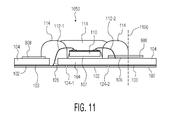
- FIG. 11 is a cross-sectional view (along a dotted line 1052 shown in FIG. 10 ) of one of the dual-interface IC chip modules 1050 depicted in FIG. 10 .
- the dual-interface IC chip module includes the contact layer 102 with the groove lines 124 - 1 , 124 - 2 , the adhesive layer 103 , the substrate 104 , the adhesive layer 106 , the two antenna contact leads 808 , the IC chip 110 , the bond wires 112 , and the encapsulation 114 .
- the adhesive layer is only applied to the area of the substrate that is covered by the encapsulation, as indicated by dotted line 1160 .
- FIG. 12 illustrates some mechanical tests for the dual-interface IC card 100 depicted in FIG. 1 . As shown in illustrated in FIG. 12 , the dual-interface IC card is bent in different degrees and angles in mechanical tests of the dual-interface IC card.
- FIG. 13 illustrates a deformation of the dual-interface IC card 100 depicted in FIG. 1 under mechanical tests.
- the antenna contact lead 108 is shifted from its original location to a new location 1080 , as shown in the dotted circle 1190 .
- FIG. 14 is a process flow diagram of a method for manufacturing a dual-interface IC card component in accordance with an embodiment of the invention.
- a single-sided contact base structure is obtained, where the single-sided contact base structure includes a substrate with an electrical contact layer.
- the single-sided contact base structure is part of a single-sided contact tape, such as the single-sided contact tape 440 shown in FIGS. 4 and 5 .
- at least one antenna contact lead is attached to the single-sided contact base structure by applying an adhesive material to partially cover an overlapping area of the at least one antenna contact and the substrate to form a dual-interface contact structure, which is a component of a dual-interface IC card.
- the dual-interface contact structure is part of a dual-interface contact tape, such as the dual-interface contact tape shown in FIGS. 8 and 9 .
- the antenna contact leads 108 are placed on the substrate 104 , and subsequently, the contact layer 102 is formed on the substrate.
- the substrate which may be a glass epoxy tape or other isolation layer.
- adhesive e.g., the adhesive 610 at FIG. 6
- the antenna contact leads are placed on the substrate.
- the adhesive is cured.
- a conductive tape is attached (e.g., laminated) to the substrate to form the contact layer 102 .
- the structure formed by the substrate and the conductive tape is separated (e.g., with laser or by etching) into different areas, which can be used for the necessary ISO (e.g., ISO/IEC 14443) areas for interconnection.
- the contact layer and the antenna contact leads are plated simultaneously or one side after the other with one or more plating materials, such as nickel (Ni), gold (Au) and palladium (Pd). Plating the contact layer and the antenna contact leads allows the contact layer and the antenna contact leads to have better appearance and/or better electrical conductivity.
- the antenna contact leads may be non-conductive and plating the antenna contact leads allows surfaces of the antenna contact leads to be conductive.
- FIG. 15 is a process flow diagram of a method for manufacturing a dual-interface IC card component in accordance with an embodiment of the invention.
- a base structure that includes a substrate is obtained.
- at least one antenna contact lead is attached to the base structure by applying an adhesive material to partially cover an overlapping area of the at least one antenna contact and the substrate to form a dual-interface contact structure, which is a component of a dual-interface IC card.
- the at least one antenna contact and the base structure are plated with at least one metal material.
Abstract
Description
Claims (18)
Priority Applications (1)
| Application Number | Priority Date | Filing Date | Title |
|---|---|---|---|
| US14/677,836 US9536188B2 (en) | 2014-04-01 | 2015-04-02 | Dual-interface IC card components and method for manufacturing the dual-interface IC card components |
Applications Claiming Priority (2)
| Application Number | Priority Date | Filing Date | Title |
|---|---|---|---|
| US14/242,031 US9424507B2 (en) | 2014-04-01 | 2014-04-01 | Dual interface IC card components and method for manufacturing the dual-interface IC card components |
| US14/677,836 US9536188B2 (en) | 2014-04-01 | 2015-04-02 | Dual-interface IC card components and method for manufacturing the dual-interface IC card components |
Related Parent Applications (1)
| Application Number | Title | Priority Date | Filing Date |
|---|---|---|---|
| US14/242,031 Continuation-In-Part US9424507B2 (en) | 2014-04-01 | 2014-04-01 | Dual interface IC card components and method for manufacturing the dual-interface IC card components |
Publications (2)
| Publication Number | Publication Date |
|---|---|
| US20150278674A1 US20150278674A1 (en) | 2015-10-01 |
| US9536188B2 true US9536188B2 (en) | 2017-01-03 |
Family
ID=54190870
Family Applications (1)
| Application Number | Title | Priority Date | Filing Date |
|---|---|---|---|
| US14/677,836 Active US9536188B2 (en) | 2014-04-01 | 2015-04-02 | Dual-interface IC card components and method for manufacturing the dual-interface IC card components |
Country Status (1)
| Country | Link |
|---|---|
| US (1) | US9536188B2 (en) |
Cited By (2)
| Publication number | Priority date | Publication date | Assignee | Title |
|---|---|---|---|---|
| US10366320B2 (en) | 2015-10-21 | 2019-07-30 | Nxp B.V. | Dual-interface IC card |
| US10461057B2 (en) | 2015-09-30 | 2019-10-29 | Nxp B.V. | Dual-interface IC card module |
Families Citing this family (4)
| Publication number | Priority date | Publication date | Assignee | Title |
|---|---|---|---|---|
| US9390365B2 (en) * | 2014-04-10 | 2016-07-12 | American Banknote Corporation | Integrated circuit module for a dual-interface smart card |
| JP6478901B2 (en) * | 2015-11-30 | 2019-03-06 | ニッタ株式会社 | IC tag, IC tag container and rubber product with IC tag |
| WO2019045638A1 (en) * | 2017-08-28 | 2019-03-07 | Smartflex Technology Pte Ltd | Integrated circuit modules and smart cards incorporating the same |
| US11350522B2 (en) * | 2019-03-26 | 2022-05-31 | Sony Corporation | Microwave antenna apparatus |
Citations (6)
| Publication number | Priority date | Publication date | Assignee | Title |
|---|---|---|---|---|
| US20030052177A1 (en) | 2001-09-14 | 2003-03-20 | Christophe Halope | Contactless or hybrid contact-contactless smart card with reinforced connection of the electronic module |
| US20090184166A1 (en) * | 2008-01-18 | 2009-07-23 | Texas Instruments Incorporated | Thin smart card module having strap on carrier |
| US20120193436A1 (en) | 2011-01-31 | 2012-08-02 | American Bank Note Company | Dual-interface smart card |
| US20130026238A1 (en) | 2011-07-12 | 2013-01-31 | Pierre Benato | Hybrid contact-contactless smart card with reinforced electronic module |
| US20130140370A1 (en) * | 2010-08-12 | 2013-06-06 | David Finn | Rfid antenna modules and methods |
| EP2626814A1 (en) | 2012-02-09 | 2013-08-14 | HID Global GmbH | Transponder comprising means for reducing bending stress on the antenna |
-
2015
- 2015-04-02 US US14/677,836 patent/US9536188B2/en active Active
Patent Citations (6)
| Publication number | Priority date | Publication date | Assignee | Title |
|---|---|---|---|---|
| US20030052177A1 (en) | 2001-09-14 | 2003-03-20 | Christophe Halope | Contactless or hybrid contact-contactless smart card with reinforced connection of the electronic module |
| US20090184166A1 (en) * | 2008-01-18 | 2009-07-23 | Texas Instruments Incorporated | Thin smart card module having strap on carrier |
| US20130140370A1 (en) * | 2010-08-12 | 2013-06-06 | David Finn | Rfid antenna modules and methods |
| US20120193436A1 (en) | 2011-01-31 | 2012-08-02 | American Bank Note Company | Dual-interface smart card |
| US20130026238A1 (en) | 2011-07-12 | 2013-01-31 | Pierre Benato | Hybrid contact-contactless smart card with reinforced electronic module |
| EP2626814A1 (en) | 2012-02-09 | 2013-08-14 | HID Global GmbH | Transponder comprising means for reducing bending stress on the antenna |
Cited By (3)
| Publication number | Priority date | Publication date | Assignee | Title |
|---|---|---|---|---|
| US10461057B2 (en) | 2015-09-30 | 2019-10-29 | Nxp B.V. | Dual-interface IC card module |
| US11222861B2 (en) | 2015-09-30 | 2022-01-11 | Nxp B.V. | Dual-interface IC card module |
| US10366320B2 (en) | 2015-10-21 | 2019-07-30 | Nxp B.V. | Dual-interface IC card |
Also Published As
| Publication number | Publication date |
|---|---|
| US20150278674A1 (en) | 2015-10-01 |
Similar Documents
| Publication | Publication Date | Title |
|---|---|---|
| US9536188B2 (en) | Dual-interface IC card components and method for manufacturing the dual-interface IC card components | |
| US11222861B2 (en) | Dual-interface IC card module | |
| US5598032A (en) | Hybrid chip card capable of both contact and contact-free operation and having antenna contacts situated in a cavity for an electronic module | |
| US5671525A (en) | Method of manufacturing a hybrid chip card | |
| US20110011939A1 (en) | Contact-less and dual interface inlays and methods for producing the same | |
| US10417548B2 (en) | Method for producing a circuit for a chip card module and circuit for a chip card module | |
| US10685275B2 (en) | Method for fabricating a smart card device | |
| US10366320B2 (en) | Dual-interface IC card | |
| US9390365B2 (en) | Integrated circuit module for a dual-interface smart card | |
| KR102190847B1 (en) | Method for manufacturing a flexible printed circuit, flexible printed circuit obtained by said method, and chip card module comprising such a flexible printed circuit | |
| US9424507B2 (en) | Dual interface IC card components and method for manufacturing the dual-interface IC card components | |
| US20110073357A1 (en) | Electronic device and method of manufacturing an electronic device | |
| US20140224882A1 (en) | Flexible Smart Card Transponder | |
| CN105453115A (en) | Method for making an anti-crack electronic device | |
| CN107111779B (en) | Method for manufacturing a single-sided electronic module comprising an interconnection zone | |
| KR20060017779A (en) | Method for mounting an electronic component on a substrante | |
| KR101209562B1 (en) | Rf antenna and the method for fabricating the same | |
| EP3079105B1 (en) | Dual-interface ic card components and method for manufacturing the dual-interface ic card components | |
| JP2007114991A (en) | Composite ic card and ic module for composite ic card | |
| KR20210060476A (en) | Method for manufacturing an electronic module for a portable object | |
| CN102468862A (en) | High frequency radio-frequency circuit embedded mobile phone expansion card sticker | |
| WO2012169873A2 (en) | Method of thermocompression bonding of laser-etched copper pads to cob module |
Legal Events
| Date | Code | Title | Description |
|---|---|---|---|
| AS | Assignment |
Owner name: NXP B.V., NETHERLANDS Free format text: ASSIGNMENT OF ASSIGNORS INTEREST;ASSIGNORS:SCHOENGRUNDNER, PATRICK;EIPER, ERNST;ZENZ, CHRISTIAN;SIGNING DATES FROM 20150331 TO 20150401;REEL/FRAME:035325/0346 |
|
| AS | Assignment |
Owner name: MORGAN STANLEY SENIOR FUNDING, INC., MARYLAND Free format text: SECURITY AGREEMENT SUPPLEMENT;ASSIGNOR:NXP B.V.;REEL/FRAME:038017/0058 Effective date: 20160218 |
|
| AS | Assignment |
Owner name: MORGAN STANLEY SENIOR FUNDING, INC., MARYLAND Free format text: CORRECTIVE ASSIGNMENT TO CORRECT THE REMOVE APPLICATION 12092129 PREVIOUSLY RECORDED ON REEL 038017 FRAME 0058. ASSIGNOR(S) HEREBY CONFIRMS THE SECURITY AGREEMENT SUPPLEMENT;ASSIGNOR:NXP B.V.;REEL/FRAME:039361/0212 Effective date: 20160218 |
|
| STCF | Information on status: patent grant |
Free format text: PATENTED CASE |
|
| AS | Assignment |
Owner name: MORGAN STANLEY SENIOR FUNDING, INC., MARYLAND Free format text: CORRECTIVE ASSIGNMENT TO CORRECT THE REMOVE APPLICATION 12681366 PREVIOUSLY RECORDED ON REEL 039361 FRAME 0212. ASSIGNOR(S) HEREBY CONFIRMS THE SECURITY AGREEMENT SUPPLEMENT;ASSIGNOR:NXP B.V.;REEL/FRAME:042762/0145 Effective date: 20160218 Owner name: MORGAN STANLEY SENIOR FUNDING, INC., MARYLAND Free format text: CORRECTIVE ASSIGNMENT TO CORRECT THE REMOVE APPLICATION 12681366 PREVIOUSLY RECORDED ON REEL 038017 FRAME 0058. ASSIGNOR(S) HEREBY CONFIRMS THE SECURITY AGREEMENT SUPPLEMENT;ASSIGNOR:NXP B.V.;REEL/FRAME:042985/0001 Effective date: 20160218 |
|
| AS | Assignment |
Owner name: NXP B.V., NETHERLANDS Free format text: RELEASE BY SECURED PARTY;ASSIGNOR:MORGAN STANLEY SENIOR FUNDING, INC.;REEL/FRAME:050745/0001 Effective date: 20190903 |
|
| AS | Assignment |
Owner name: MORGAN STANLEY SENIOR FUNDING, INC., MARYLAND Free format text: CORRECTIVE ASSIGNMENT TO CORRECT THE REMOVE APPLICATION 12298143 PREVIOUSLY RECORDED ON REEL 039361 FRAME 0212. ASSIGNOR(S) HEREBY CONFIRMS THE SECURITY AGREEMENT SUPPLEMENT;ASSIGNOR:NXP B.V.;REEL/FRAME:051029/0387 Effective date: 20160218 Owner name: MORGAN STANLEY SENIOR FUNDING, INC., MARYLAND Free format text: CORRECTIVE ASSIGNMENT TO CORRECT THE REMOVE APPLICATION 12298143 PREVIOUSLY RECORDED ON REEL 042985 FRAME 0001. ASSIGNOR(S) HEREBY CONFIRMS THE SECURITY AGREEMENT SUPPLEMENT;ASSIGNOR:NXP B.V.;REEL/FRAME:051029/0001 Effective date: 20160218 Owner name: MORGAN STANLEY SENIOR FUNDING, INC., MARYLAND Free format text: CORRECTIVE ASSIGNMENT TO CORRECT THE REMOVE APPLICATION 12298143 PREVIOUSLY RECORDED ON REEL 042762 FRAME 0145. ASSIGNOR(S) HEREBY CONFIRMS THE SECURITY AGREEMENT SUPPLEMENT;ASSIGNOR:NXP B.V.;REEL/FRAME:051145/0184 Effective date: 20160218 Owner name: MORGAN STANLEY SENIOR FUNDING, INC., MARYLAND Free format text: CORRECTIVE ASSIGNMENT TO CORRECT THE REMOVE APPLICATION 12298143 PREVIOUSLY RECORDED ON REEL 038017 FRAME 0058. ASSIGNOR(S) HEREBY CONFIRMS THE SECURITY AGREEMENT SUPPLEMENT;ASSIGNOR:NXP B.V.;REEL/FRAME:051030/0001 Effective date: 20160218 Owner name: MORGAN STANLEY SENIOR FUNDING, INC., MARYLAND Free format text: CORRECTIVE ASSIGNMENT TO CORRECT THE REMOVE APPLICATION12298143 PREVIOUSLY RECORDED ON REEL 042985 FRAME 0001. ASSIGNOR(S) HEREBY CONFIRMS THE SECURITY AGREEMENT SUPPLEMENT;ASSIGNOR:NXP B.V.;REEL/FRAME:051029/0001 Effective date: 20160218 Owner name: MORGAN STANLEY SENIOR FUNDING, INC., MARYLAND Free format text: CORRECTIVE ASSIGNMENT TO CORRECT THE REMOVE APPLICATION12298143 PREVIOUSLY RECORDED ON REEL 039361 FRAME 0212. ASSIGNOR(S) HEREBY CONFIRMS THE SECURITY AGREEMENT SUPPLEMENT;ASSIGNOR:NXP B.V.;REEL/FRAME:051029/0387 Effective date: 20160218 Owner name: MORGAN STANLEY SENIOR FUNDING, INC., MARYLAND Free format text: CORRECTIVE ASSIGNMENT TO CORRECT THE REMOVE APPLICATION12298143 PREVIOUSLY RECORDED ON REEL 042762 FRAME 0145. ASSIGNOR(S) HEREBY CONFIRMS THE SECURITY AGREEMENT SUPPLEMENT;ASSIGNOR:NXP B.V.;REEL/FRAME:051145/0184 Effective date: 20160218 |
|
| MAFP | Maintenance fee payment |
Free format text: PAYMENT OF MAINTENANCE FEE, 4TH YEAR, LARGE ENTITY (ORIGINAL EVENT CODE: M1551); ENTITY STATUS OF PATENT OWNER: LARGE ENTITY Year of fee payment: 4 |