US9535513B2 - Thin electromagnetic handwriting pen and method of manufacturing the same - Google Patents
Thin electromagnetic handwriting pen and method of manufacturing the same Download PDFInfo
- Publication number
- US9535513B2 US9535513B2 US14/280,650 US201414280650A US9535513B2 US 9535513 B2 US9535513 B2 US 9535513B2 US 201414280650 A US201414280650 A US 201414280650A US 9535513 B2 US9535513 B2 US 9535513B2
- Authority
- US
- United States
- Prior art keywords
- pen
- thin
- outer tube
- coil
- electromagnetic
- Prior art date
- Legal status (The legal status is an assumption and is not a legal conclusion. Google has not performed a legal analysis and makes no representation as to the accuracy of the status listed.)
- Active
Links
Images


Classifications
-
- G—PHYSICS
- G06—COMPUTING; CALCULATING OR COUNTING
- G06F—ELECTRIC DIGITAL DATA PROCESSING
- G06F3/00—Input arrangements for transferring data to be processed into a form capable of being handled by the computer; Output arrangements for transferring data from processing unit to output unit, e.g. interface arrangements
- G06F3/01—Input arrangements or combined input and output arrangements for interaction between user and computer
- G06F3/03—Arrangements for converting the position or the displacement of a member into a coded form
- G06F3/033—Pointing devices displaced or positioned by the user, e.g. mice, trackballs, pens or joysticks; Accessories therefor
- G06F3/0354—Pointing devices displaced or positioned by the user, e.g. mice, trackballs, pens or joysticks; Accessories therefor with detection of 2D relative movements between the device, or an operating part thereof, and a plane or surface, e.g. 2D mice, trackballs, pens or pucks
- G06F3/03545—Pens or stylus
-
- G—PHYSICS
- G06—COMPUTING; CALCULATING OR COUNTING
- G06F—ELECTRIC DIGITAL DATA PROCESSING
- G06F3/00—Input arrangements for transferring data to be processed into a form capable of being handled by the computer; Output arrangements for transferring data from processing unit to output unit, e.g. interface arrangements
- G06F3/01—Input arrangements or combined input and output arrangements for interaction between user and computer
- G06F3/03—Arrangements for converting the position or the displacement of a member into a coded form
- G06F3/033—Pointing devices displaced or positioned by the user, e.g. mice, trackballs, pens or joysticks; Accessories therefor
- G06F3/039—Accessories therefor, e.g. mouse pads
- G06F3/0393—Accessories for touch pads or touch screens, e.g. mechanical guides added to touch screens for drawing straight lines, hard keys overlaying touch screens or touch pads
-
- G—PHYSICS
- G06—COMPUTING; CALCULATING OR COUNTING
- G06F—ELECTRIC DIGITAL DATA PROCESSING
- G06F3/00—Input arrangements for transferring data to be processed into a form capable of being handled by the computer; Output arrangements for transferring data from processing unit to output unit, e.g. interface arrangements
- G06F3/01—Input arrangements or combined input and output arrangements for interaction between user and computer
- G06F3/03—Arrangements for converting the position or the displacement of a member into a coded form
- G06F3/041—Digitisers, e.g. for touch screens or touch pads, characterised by the transducing means
- G06F3/044—Digitisers, e.g. for touch screens or touch pads, characterised by the transducing means by capacitive means
- G06F3/0442—Digitisers, e.g. for touch screens or touch pads, characterised by the transducing means by capacitive means using active external devices, e.g. active pens, for transmitting changes in electrical potential to be received by the digitiser
-
- H—ELECTRICITY
- H01—ELECTRIC ELEMENTS
- H01F—MAGNETS; INDUCTANCES; TRANSFORMERS; SELECTION OF MATERIALS FOR THEIR MAGNETIC PROPERTIES
- H01F27/00—Details of transformers or inductances, in general
- H01F27/28—Coils; Windings; Conductive connections
-
- H—ELECTRICITY
- H01—ELECTRIC ELEMENTS
- H01F—MAGNETS; INDUCTANCES; TRANSFORMERS; SELECTION OF MATERIALS FOR THEIR MAGNETIC PROPERTIES
- H01F7/00—Magnets
- H01F7/06—Electromagnets; Actuators including electromagnets
- H01F7/08—Electromagnets; Actuators including electromagnets with armatures
- H01F7/126—Supporting or mounting
-
- H—ELECTRICITY
- H01—ELECTRIC ELEMENTS
- H01F—MAGNETS; INDUCTANCES; TRANSFORMERS; SELECTION OF MATERIALS FOR THEIR MAGNETIC PROPERTIES
- H01F7/00—Magnets
- H01F7/06—Electromagnets; Actuators including electromagnets
- H01F7/08—Electromagnets; Actuators including electromagnets with armatures
- H01F7/16—Rectilinearly-movable armatures
- H01F7/1607—Armatures entering the winding
-
- G—PHYSICS
- G06—COMPUTING; CALCULATING OR COUNTING
- G06F—ELECTRIC DIGITAL DATA PROCESSING
- G06F3/00—Input arrangements for transferring data to be processed into a form capable of being handled by the computer; Output arrangements for transferring data from processing unit to output unit, e.g. interface arrangements
- G06F3/01—Input arrangements or combined input and output arrangements for interaction between user and computer
- G06F3/03—Arrangements for converting the position or the displacement of a member into a coded form
- G06F3/041—Digitisers, e.g. for touch screens or touch pads, characterised by the transducing means
- G06F3/046—Digitisers, e.g. for touch screens or touch pads, characterised by the transducing means by electromagnetic means
Definitions
- the instant disclosure relates to an electromagnetic handwriting pen and a method of manufacturing the same, and more particularly to a thin electromagnetic handwriting pen and a method of manufacturing the same.
- Conventional touch control devices may be classified into three types: resistive, electromagnetic and capacitive. Operation with a resistive touch control device requires a rigid pen tip to apply a significant force on the resistive touch control device in a very small area to accomplish deformation of the resistive touch sensor, and an electromagnetic touch control device requires a special battery powered pen for input; while the working principle of a capacitive touch control device relies on capacitive coupling, which takes place as soon as the capacitive touch sensor is touched by a conductive object, and the touch position can then be identified according to the variation in capacitance at the touch point. Therefore, a capacitive touch control device does not require an input pen that consumes electricity.
- capacitive touch control device has a longer service life.
- mass production of capacitive touch control devices requires lower costs due to its simple construction, less components and higher yield rate.
- a capacitive touch control device can be operated in many ways. The most common of all is using a conductor, for example a finger or a pen, to touch or slide on the surface of the capacitive touch control device, for the capacitive touch sensor thereof to generate a response signal.
- a conductor for example a finger or a pen
- the lower precision on position detection tends to hinder smoothness of operation where more precise and more efficient detection is required, such as in handheld devices.
- many people choose to use pens for capacitive touch input.
- One aspect of the instant disclosure relates to a thin electromagnetic handwriting pen and a method of manufacturing the same.
- a thin electromagnetic handwriting pen comprising: a casing unit, a circuit unit, an electromagnetic unit, a pen core unit, a connection unit and an elastic unit.
- the casing unit includes a thin pen-shaped casing structure.
- the circuit unit includes a circuit substrate disposed inside the thin pen-shaped casing structure.
- the electromagnetic unit includes a hollow holder and an electromagnetic coil wound around the hollow holder, wherein both the hollow holder and the electromagnetic coil are embedded in the thin pen-shaped casing structure, and the electromagnetic coil is fixed between the thin pen-shaped casing structure and the hollow holder and electrically connected to the circuit substrate.
- the pen core unit includes a pen core structure movably disposed inside the thin pen-shaped casing structure and passing through the hollow holder, wherein one portion of the pen core structure is exposed outside the thin pen-shaped casing structure.
- the connection unit includes a connection structure disposed inside the thin pen-shaped casing structure and positioned on the circuit substrate.
- the elastic unit includes an elastic structure disposed inside the thin pen-shaped casing structure and connected between the pen core structure and the connection structure.
- the thin pen-shaped casing structure includes a first hollow outer tube, a second hollow outer tube and a pen tail cover, and the second hollow outer tube has two opposite lateral portions respectively mated with the first hollow outer tube and the pen tail cover, wherein the second hollow outer tube has a stop portion disposed on the inner surface thereof, the circuit substrate has an abutting portion abutted against the stop portion of the second hollow outer tube, and the circuit substrate has at least two positioning holes adjacent to the connection structure and at least one positioning groove adjacent to the connection structure.
- the hollow holder has a coil winding portion and a coil guiding portion connected to the coil winding portion, the coil winding portion has a coil winding space, and the coil guiding portion has at least two coil guiding grooves communicated with the coil winding space, wherein the electromagnetic coil has a main coil portion wound around the coil winding portion and received in the coil winding space and two guiding coil portions respectively connected to two opposite ends of the main coil portion and respectively received in the at least two coil guiding grooves, and the main coil portion of the electromagnetic coil is totally enclosed inside the first hollow outer tube, and each guiding coil portion of the electromagnetic coil has a soldering portion exposed outside the first hollow outer tube to electrically connect to the circuit substrate.
- the pen core structure includes a metal pen core movably passing through the hollow holder and a plastic pen head connected to one end of the metal pen core, and one portion of the plastic pen head is exposed outside the first hollow outer tube of the thin pen-shaped casing structure.
- a thin electromagnetic handwriting pen comprising: a casing unit, a circuit unit, an electromagnetic unit and a pen core unit.
- the casing unit includes a thin pen-shaped casing structure.
- the circuit unit includes a circuit substrate disposed inside the thin pen-shaped casing structure.
- the electromagnetic unit includes a hollow holder and an electromagnetic coil wound around the hollow holder, wherein both the hollow holder and the electromagnetic coil are embedded in the thin pen-shaped casing structure, and the electromagnetic coil is fixed between the thin pen-shaped casing structure and the hollow holder and electrically connected to the circuit substrate.
- the pen core unit includes a pen core structure movably disposed inside the thin pen-shaped casing structure and passing through the hollow holder, wherein one portion of the pen core structure is exposed outside the thin pen-shaped casing structure.
- Yet another one of the embodiments of the instant disclosure provides a method of manufacturing a thin electromagnetic handwriting pen, comprising: winding an electromagnetic coil around a hollow holder; forming a first hollow outer tube to enclose the electromagnetic coil and fix the electromagnetic coil between the first hollow outer tube and the hollow holder, wherein the electromagnetic coil has two soldering portions exposed outside the first hollow outer tube; sequentially inserting a pen core structure, an elastic structure, a connection structure and one portion of a circuit substrate into the first hollow outer tube, wherein one portion of the pen core structure is exposed outside the first hollow outer tube; electrically connecting the two soldering portions of the electromagnetic coil to the circuit substrate; and mating a second hollow outer tube with the first hollow outer tube and mating a pen tail cover with the second hollow outer tube for enclosing the other portion of the circuit substrate.
- the electromagnetic coil can be fixed between the thin pen-shaped casing structure and the hollow holder and electrically connected to the circuit substrate due to the design of both the hollow holder and the electromagnetic coil are embedded in the thin pen-shaped casing structure and the processes of winding an electromagnetic coil around a hollow holder and forming a first hollow outer tube to enclose the electromagnetic coil.
- the hollow holder and the electromagnetic coil of the electromagnetic unit can be fixed inside the thin pen-shaped casing structure without using any prior detachable holder to occupy the thickness of the thin pen-shaped casing structure, so as to achieve the thin design of the thin electromagnetic handwriting pen.
- the thin electromagnetic handwriting pen can be applied to the thin portable electronic device, for example, the thin electromagnetic handwriting pen can be inserted into the edge hole of the thin portable electronic device.
- FIG. 1 shows a flow chart of the method of manufacturing a thin electromagnetic handwriting pen according to the instant disclosure
- FIG. 2 shows a perspective, schematic view of the hollow holder of the thin electromagnetic handwriting pen according to the instant disclosure
- FIG. 3 shows a perspective, schematic view of the step S 100 of the method of manufacturing a thin electromagnetic handwriting pen according to the instant disclosure
- FIG. 4 shows a perspective, schematic view of the step S 102 of the method of manufacturing a thin electromagnetic handwriting pen according to the instant disclosure
- FIG. 5 shows a lateral, cross-sectional, schematic view of the step S 102 of the method of manufacturing a thin electromagnetic handwriting pen according to the instant disclosure
- FIG. 6 shows a perspective, schematic view of the step S 104 and the step S 106 of the method of manufacturing a thin electromagnetic handwriting pen according to the instant disclosure
- FIG. 7 shows a lateral, cross-sectional, schematic view of the step S 104 and the step S 106 of the method of manufacturing a thin electromagnetic handwriting pen according to the instant disclosure
- FIG. 8 shows a perspective, schematic view of the step S 108 of the method of manufacturing a thin electromagnetic handwriting pen according to the instant disclosure
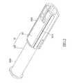
- FIG. 9 shows a lateral, schematic view of the thin electromagnetic handwriting pen according to the instant disclosure.
- FIG. 10 shows a perspective, exploded, schematic view of the thin electromagnetic handwriting pen according to the instant disclosure.
- the instant disclosure provides a method of manufacturing a thin (or flat) electromagnetic handwriting pen Z, comprising the following steps:
- step S 100 is that: referring to FIG. 1 , FIG. 2 and FIG. 3 , winding an electromagnetic coil 31 around a hollow holder 30 .
- the hollow holder 30 has a coil winding portion 300 and a coil guiding portion 301 connected to the coil winding portion 300 .
- the coil winding portion 300 has a coil winding space 3000 as a surrounding shape formed therearound, and the coil guiding portion 301 has at least two coil guiding grooves 3010 communicated with the coil winding space 3000 .
- FIG. 1 the hollow holder 30
- the hollow holder 30 has a coil winding portion 300 and a coil guiding portion 301 connected to the coil winding portion 300 .
- the coil winding portion 300 has a coil winding space 3000 as a surrounding shape formed therearound, and the coil guiding portion 301 has at least two coil guiding grooves 3010 communicated with the coil winding space 3000 .
- the electromagnetic coil 31 has a main coil portion 310 wound around the coil winding portion 300 and received in the coil winding space 3000 and two guiding coil portions 311 respectively connected to two opposite ends of the main coil portion 310 and respectively received in the at least two coil guiding grooves 3010 .
- the hollow holder 30 may be made of any high temperature resistant material, and the electromagnetic coil 31 may be an enamel-insulated wire.
- step S 102 is that: referring to FIG. 1 , FIG. 4 and FIG. 5 , forming a first hollow outer tube 101 to enclose the electromagnetic coil 31 and fix the electromagnetic coil 31 between the first hollow outer tube 101 and the hollow holder 30 , wherein the electromagnetic coil 31 has two soldering portions 3110 exposed outside the first hollow outer tube 101 . More precisely, both the hollow holder 30 and the electromagnetic coil 31 are embedded in the first hollow outer tube 101 , the main coil portion 310 of the electromagnetic coil 31 is totally enclosed inside the first hollow outer tube 101 , and the soldering portion 3110 of each guiding coil portion 311 of the electromagnetic coil 31 is exposed outside the first hollow outer tube 101 to prepare to electrically connect with the circuit substrate 20 .
- the first hollow outer tube 101 may be formed by an injection molding process or other forming process, and the electromagnetic coil 31 is enclosed by forming the first hollow outer tube 101 .
- step S 104 is that: referring to FIG. 1 , FIG. 6 and FIG. 7 , sequentially inserting a pen core structure 40 , an elastic structure 60 , a connection structure 50 and one portion of a circuit substrate 20 into the first hollow outer tube 101 , wherein one portion of the pen core structure 40 is exposed outside the first hollow outer tube 101 .
- the pen core structure 40 is movably disposed inside the first hollow outer tube 101 and passes through the hollow holder 30
- the connection structure 50 is positioned on the circuit substrate 20
- the elastic structure 60 is connected between the pen core structure 40 and the connection structure 50 .
- the connection structure 50 is positioned on the front side portion of the circuit substrate 20 in advance, thus the connection structure 50 and the circuit substrate 20 are concurrently placed inside the first hollow outer tube 101 .
- step S 106 is that: referring to FIG. 1 , FIG. 6 and FIG. 7 , electrically connecting the two soldering portions 3110 of the electromagnetic coil 31 to the circuit substrate 20 .
- the two soldering portions 3110 of the electromagnetic coil 31 are respectively soldered on two conductive pads (not labeled) that are disposed on the top surface of the circuit substrate 20 .
- step S 108 is that: referring to FIG. 1 , FIG. 8 and FIG. 9 , mating a second hollow outer tube 102 with the first hollow outer tube 101 and mating a pen tail cover 103 with the second hollow outer tube 102 for enclosing the other portion of the circuit substrate 20 . More precisely, the first hollow outer tube 101 , the second hollow outer tube 102 and the pen tail cover 103 are mated with each other to form a thin pen-shaped casing structure 10 , but it is merely an example and is not meant to limit the instant disclosure. It is worth noting that, referring to FIG.
- the thin electromagnetic handwriting pen Z can be applied to the thin portable electronic device (not shown), for example, the thin electromagnetic handwriting pen Z can be inserted into the edge hole of the thin portable electronic device (not shown).
- the instant disclosure provides a thin electromagnetic handwriting pen Z manufactured through the step S 100 to the step S 108 , and the thin electromagnetic handwriting pen Z comprises a casing unit 1 , a circuit unit 2 , an electromagnetic unit 3 , a pen core unit 4 , a connection unit 5 and an elastic unit 6 .
- the casing unit 1 includes a thin pen-shaped casing structure 10
- the circuit unit 2 includes a circuit substrate 20 disposed inside the thin pen-shaped casing structure 10
- the thin pen-shaped casing structure 10 includes a first hollow outer tube 101 , a second hollow outer tube 102 and a pen tail cover 103
- the second hollow outer tube 102 has two opposite lateral portions respectively mated with the first hollow outer tube 101 and the pen tail cover 103 .
- the second hollow outer tube 102 has a stop portion 1020 disposed on the inner surface thereof, and the circuit substrate 20 has an abutting portion 200 backwardly abutted against the stop portion 1020 of the second hollow outer tube 102 .
- the circuit substrate 20 has at least two positioning holes 201 adjacent to the connection structure 50 and at least one positioning groove 202 adjacent to the connection structure 50 , and the positioning groove 202 is substantially disposed between one of the two positioning holes 201 and the connection structure 50 .
- the electromagnetic unit 3 includes a hollow holder 30 and an electromagnetic coil 31 wound around the hollow holder 30 .
- Both the hollow holder 30 and the electromagnetic coil 31 are embedded in the thin pen-shaped casing structure 10 , and the electromagnetic coil 31 is fixed between the thin pen-shaped casing structure 10 and the hollow holder 30 and electrically connected to the circuit substrate 20 through the two soldering portions 3110 .
- the hollow holder 30 has a coil winding portion 300 and a coil guiding portion 301 connected to the coil winding portion 300 .
- the coil winding portion 300 has a coil winding space 3000
- the coil guiding portion 301 has at least two coil guiding grooves 3010 communicated with the coil winding space 3000 .
- the electromagnetic coil 31 has a main coil portion 310 wound around the coil winding portion 300 and received in the coil winding space 3000 and two guiding coil portions 311 respectively connected to two opposite ends of the main coil portion 310 and respectively received in the at least two coil guiding grooves 3010 .
- the main coil portion 310 of the electromagnetic coil 31 is totally enclosed inside the first hollow outer tube 101 , and the soldering portion 3110 of each guiding coil portion 311 of the electromagnetic coil 31 is exposed outside the first hollow outer tube 101 to electrically connect with the soldering portion 3110 of the circuit substrate 20 .
- the pen core unit 4 includes a pen core structure 40 movably disposed inside the thin pen-shaped casing structure 10 and passing through the hollow holder 30 , and one portion of the pen core structure 40 is exposed outside the thin pen-shaped casing structure 10 .
- the pen core structure 40 includes a metal pen core 401 (such as an iron core or any conductive material) movably passing through the hollow holder 30 and a plastic pen head 402 connected to one end of the metal pen core 401 , and one portion of the plastic pen head 402 is exposed outside the first hollow outer tube 101 of the thin pen-shaped casing structure 10 .
- connection unit 5 includes a connection structure 50 disposed inside the thin pen-shaped casing structure 10 and positioned on the circuit substrate 20
- the elastic unit 6 includes an elastic structure 60 disposed inside the thin pen-shaped casing structure 10 and connected between the pen core structure 40 and the connection structure 50
- the connection structure 50 has at least two positioning posts 500 disposed on the bottom side thereof and respectively passing through the at least two positioning holes 201 and at least one positioning block 501 disposed on the bottom side thereof and retained in the at least one positioning groove 202
- the connection structure 50 has a convex post 502 disposed on a lateral side thereof and facing the elastic structure 60 .
- the elastic structure 60 includes a first elastic element 601 (such as a compression spring or an elastic piece) disposed around the convex post 502 and a second elastic element 602 (such as a compression spring or an elastic piece) disposed between another end of the metal pen core 401 and the convex post 502 of the connection structure 50 and contacting the first elastic element 601 , and the two opposite ends of the second elastic element 602 are respectively abutted against another end of the metal pen core 401 and the convex post 502 of the connection structure 50 .
- a first elastic element 601 such as a compression spring or an elastic piece
- a second elastic element 602 such as a compression spring or an elastic piece
- the electromagnetic coil 31 can be fixed between the thin pen-shaped casing structure 10 and the hollow holder 30 and electrically connected to the circuit substrate 20 due to the design of both the hollow holder 30 and the electromagnetic coil 31 are embedded in the thin pen-shaped casing structure 10 and the processes of winding an electromagnetic coil 31 around a hollow holder 30 and forming a first hollow outer tube 101 to enclose the electromagnetic coil 31 .
- the hollow holder 30 and the electromagnetic coil 31 of the electromagnetic unit 3 can be fixed inside the thin pen-shaped casing structure Z without using any prior detachable holder to occupy the thickness of the thin pen-shaped casing structure Z, so as to achieve the thin design of the thin electromagnetic handwriting pen Z.
- the thin electromagnetic handwriting pen Z can be applied to the thin portable electronic device (not shown), for example, the thin electromagnetic handwriting pen Z can be inserted into the edge hole of the thin portable electronic device (not shown).
Landscapes
- Engineering & Computer Science (AREA)
- Physics & Mathematics (AREA)
- General Engineering & Computer Science (AREA)
- Theoretical Computer Science (AREA)
- Power Engineering (AREA)
- Electromagnetism (AREA)
- Human Computer Interaction (AREA)
- General Physics & Mathematics (AREA)
- Position Input By Displaying (AREA)
- Media Introduction/Drainage Providing Device (AREA)
Priority Applications (1)
| Application Number | Priority Date | Filing Date | Title |
|---|---|---|---|
| US15/331,129 US10180737B2 (en) | 2014-01-29 | 2016-10-21 | Thin electromagnetic handwriting pen and method of manufacturing the same |
Applications Claiming Priority (3)
| Application Number | Priority Date | Filing Date | Title |
|---|---|---|---|
| TW103103491A | 2014-01-29 | ||
| TW103103491A TWI529567B (zh) | 2014-01-29 | 2014-01-29 | 薄形化電磁式手寫筆及其製作方法 |
| TW103103491 | 2014-01-29 |
Related Child Applications (1)
| Application Number | Title | Priority Date | Filing Date |
|---|---|---|---|
| US15/331,129 Continuation US10180737B2 (en) | 2014-01-29 | 2016-10-21 | Thin electromagnetic handwriting pen and method of manufacturing the same |
Publications (2)
| Publication Number | Publication Date |
|---|---|
| US20150212606A1 US20150212606A1 (en) | 2015-07-30 |
| US9535513B2 true US9535513B2 (en) | 2017-01-03 |
Family
ID=53679009
Family Applications (2)
| Application Number | Title | Priority Date | Filing Date |
|---|---|---|---|
| US14/280,650 Active US9535513B2 (en) | 2014-01-29 | 2014-05-18 | Thin electromagnetic handwriting pen and method of manufacturing the same |
| US15/331,129 Active 2034-07-24 US10180737B2 (en) | 2014-01-29 | 2016-10-21 | Thin electromagnetic handwriting pen and method of manufacturing the same |
Family Applications After (1)
| Application Number | Title | Priority Date | Filing Date |
|---|---|---|---|
| US15/331,129 Active 2034-07-24 US10180737B2 (en) | 2014-01-29 | 2016-10-21 | Thin electromagnetic handwriting pen and method of manufacturing the same |
Country Status (3)
| Country | Link |
|---|---|
| US (2) | US9535513B2 (zh) |
| CN (1) | CN104808887A (zh) |
| TW (1) | TWI529567B (zh) |
Families Citing this family (3)
| Publication number | Priority date | Publication date | Assignee | Title |
|---|---|---|---|---|
| TWI552032B (zh) * | 2015-10-20 | 2016-10-01 | 翰碩電子股份有限公司 | 電容式指標裝置 |
| JP6547637B2 (ja) * | 2016-01-15 | 2019-07-24 | Tdk株式会社 | 電子ペン用コイル装置 |
| CN114294466A (zh) * | 2022-01-13 | 2022-04-08 | 东莞市盈森汽车电喷科技有限公司 | 一种电磁线圈电阻连接结构及焊接工艺 |
Citations (11)
| Publication number | Priority date | Publication date | Assignee | Title |
|---|---|---|---|---|
| US5895895A (en) * | 1995-12-27 | 1999-04-20 | Pilot Precision Kabushiki Kaisha | Input pen |
| US6623136B1 (en) | 2002-05-16 | 2003-09-23 | Chin-Yi Kuo | Pen with lighted scanner pen head and twist switch |
| US7202862B1 (en) * | 2004-03-03 | 2007-04-10 | Finepoint Innovations, Inc. | Pressure sensor for a digitizer pen |
| US20100038152A1 (en) * | 2005-03-01 | 2010-02-18 | Wacom Co. Ltd | Position pointing device and hand-held electronic appliance |
| US20110175854A1 (en) * | 2010-01-15 | 2011-07-21 | Waltop International Corporation | Electromagnetic pointer |
| US20120146913A1 (en) * | 2010-12-13 | 2012-06-14 | Hand Held Products, Inc. | Portable data terminal stylus with rolling ball tip |
| TWM445213U (zh) * | 2012-08-07 | 2013-01-11 | Waltop Int Corp | 電磁式指標裝置 |
| EP2650761A2 (en) | 2012-04-13 | 2013-10-16 | Wacom Co., Ltd. | Position indicator |
| US20140069532A1 (en) * | 2012-09-13 | 2014-03-13 | Wacom Co., Ltd. | Position indicator of electromagnetic induction system and electronic ink cartridge |
| US20140118311A1 (en) * | 2012-10-25 | 2014-05-01 | Waltop International Corporation | Electromagnetic pen with electromagnetic and ink writing functions |
| US20150035807A1 (en) * | 2013-08-03 | 2015-02-05 | Wacom Co., Ltd. | Pen pressure detecting module and position indicator |
Family Cites Families (3)
| Publication number | Priority date | Publication date | Assignee | Title |
|---|---|---|---|---|
| US6744426B1 (en) * | 1999-08-10 | 2004-06-01 | Brother Kogyo Kabushiki Kaisha | Pen coordinate reading device with pen attribute detecting function |
| CN102200848A (zh) * | 2010-03-25 | 2011-09-28 | 深圳富泰宏精密工业有限公司 | 触控笔 |
| CN202870758U (zh) * | 2012-10-30 | 2013-04-10 | 太瀚科技股份有限公司 | 兼具电磁与墨水书写功能的电磁笔 |
-
2014
- 2014-01-29 TW TW103103491A patent/TWI529567B/zh active
- 2014-02-18 CN CN201410054683.9A patent/CN104808887A/zh active Pending
- 2014-05-18 US US14/280,650 patent/US9535513B2/en active Active
-
2016
- 2016-10-21 US US15/331,129 patent/US10180737B2/en active Active
Patent Citations (14)
| Publication number | Priority date | Publication date | Assignee | Title |
|---|---|---|---|---|
| US5895895A (en) * | 1995-12-27 | 1999-04-20 | Pilot Precision Kabushiki Kaisha | Input pen |
| US6623136B1 (en) | 2002-05-16 | 2003-09-23 | Chin-Yi Kuo | Pen with lighted scanner pen head and twist switch |
| US7202862B1 (en) * | 2004-03-03 | 2007-04-10 | Finepoint Innovations, Inc. | Pressure sensor for a digitizer pen |
| US20100038152A1 (en) * | 2005-03-01 | 2010-02-18 | Wacom Co. Ltd | Position pointing device and hand-held electronic appliance |
| US20110175854A1 (en) * | 2010-01-15 | 2011-07-21 | Waltop International Corporation | Electromagnetic pointer |
| US20120146913A1 (en) * | 2010-12-13 | 2012-06-14 | Hand Held Products, Inc. | Portable data terminal stylus with rolling ball tip |
| TW201403399A (zh) | 2012-04-13 | 2014-01-16 | Wacom Co Ltd | 位置指示器 |
| EP2650761A2 (en) | 2012-04-13 | 2013-10-16 | Wacom Co., Ltd. | Position indicator |
| US20130269446A1 (en) | 2012-04-13 | 2013-10-17 | Wacom Co., Ltd. | Position indicator |
| TWM445213U (zh) * | 2012-08-07 | 2013-01-11 | Waltop Int Corp | 電磁式指標裝置 |
| US20140043300A1 (en) * | 2012-08-07 | 2014-02-13 | Chien-Chia Lien | Electromagnetic pointer |
| US20140069532A1 (en) * | 2012-09-13 | 2014-03-13 | Wacom Co., Ltd. | Position indicator of electromagnetic induction system and electronic ink cartridge |
| US20140118311A1 (en) * | 2012-10-25 | 2014-05-01 | Waltop International Corporation | Electromagnetic pen with electromagnetic and ink writing functions |
| US20150035807A1 (en) * | 2013-08-03 | 2015-02-05 | Wacom Co., Ltd. | Pen pressure detecting module and position indicator |
Non-Patent Citations (1)
| Title |
|---|
| Taiwanese Office Action dated May 26, 2015, for corresponding TW Application No. 103103491, 6 pages. |
Also Published As
| Publication number | Publication date |
|---|---|
| US20150212606A1 (en) | 2015-07-30 |
| TWI529567B (zh) | 2016-04-11 |
| CN104808887A (zh) | 2015-07-29 |
| TW201530366A (zh) | 2015-08-01 |
| US20170038858A1 (en) | 2017-02-09 |
| US10180737B2 (en) | 2019-01-15 |
Similar Documents
| Publication | Publication Date | Title |
|---|---|---|
| US20150212605A1 (en) | Active capacitive touch pen for providing an adjustable electromagnetic field | |
| US9703401B2 (en) | Portable electronic device and miniaturization rechargeable capacitive stylus thereof | |
| US10599272B2 (en) | Portable electronic device and active capacitive stylus thereof | |
| US10551943B2 (en) | Micro touch pen structure including pen core with stop portion that moves together with magnetic unit when pressure is applied to movable portion of pen core | |
| US9274618B2 (en) | Active capacitive touch pen | |
| TWI649679B (zh) | Position indicator | |
| US20160313812A1 (en) | Position indicating module and stylus pen | |
| US10180737B2 (en) | Thin electromagnetic handwriting pen and method of manufacturing the same | |
| US9600095B2 (en) | Position indicator | |
| US20160320868A1 (en) | Rechargeable capacitive stylus | |
| US20150084935A1 (en) | Electromagnetic and capacitive pointer | |
| US9606642B2 (en) | Portable electronic device and miniaturization rechargeable capacitive stylus thereof | |
| US9939931B2 (en) | Position indicator and position detecting device | |
| US20150084934A1 (en) | Electromagnetic and capacitive pointer | |
| US8928634B2 (en) | Active electromagnetic pen | |
| TWI546706B (zh) | 電容筆 | |
| TWM566358U (zh) | Stylus stylus and stylus | |
| TWM468069U (zh) | 卡連接器改良結構 | |
| JP2015125753A (ja) | 位置指示器 | |
| KR20140059582A (ko) | 디지털 펜 |
Legal Events
| Date | Code | Title | Description |
|---|---|---|---|
| AS | Assignment |
Owner name: WALTOP INTERNATIONAL CORPORATION, TAIWAN Free format text: ASSIGNMENT OF ASSIGNORS INTEREST;ASSIGNORS:LIEN, CHIEN-CHIA;WANG, HUNG-I;LIU, CHENG-LU;SIGNING DATES FROM 20140213 TO 20140220;REEL/FRAME:032919/0401 |
|
| AS | Assignment |
Owner name: WACOM CO., LTD., JAPAN Free format text: ASSIGNMENT OF ASSIGNORS INTEREST;ASSIGNOR:WALTOP INTERNATIONAL CORPORATION;REEL/FRAME:035236/0409 Effective date: 20150305 |
|
| STCF | Information on status: patent grant |
Free format text: PATENTED CASE |
|
| MAFP | Maintenance fee payment |
Free format text: PAYMENT OF MAINTENANCE FEE, 4TH YEAR, LARGE ENTITY (ORIGINAL EVENT CODE: M1551); ENTITY STATUS OF PATENT OWNER: LARGE ENTITY Year of fee payment: 4 |