US9535281B2 - Display panel comprising first and second magenetic layers, display device comprising the same, and method for fabricating the display panel - Google Patents

Display panel comprising first and second magenetic layers, display device comprising the same, and method for fabricating the display panel Download PDF

Info

Publication number
US9535281B2
US9535281B2 US14/500,620 US201414500620A US9535281B2 US 9535281 B2 US9535281 B2 US 9535281B2 US 201414500620 A US201414500620 A US 201414500620A US 9535281 B2 US9535281 B2 US 9535281B2
Authority
US
United States
Prior art keywords
substrate
magnetic layer
display panel
magnetic
layer
Prior art date
Legal status (The legal status is an assumption and is not a legal conclusion. Google has not performed a legal analysis and makes no representation as to the accuracy of the status listed.)
Active, expires
Application number
US14/500,620
Other versions
US20150346544A1 (en
Inventor
Jun Wu
Hongming Zhan
Chao Tian
Current Assignee (The listed assignees may be inaccurate. Google has not performed a legal analysis and makes no representation or warranty as to the accuracy of the list.)
BOE Technology Group Co Ltd
Beijing BOE Display Technology Co Ltd
Original Assignee
BOE Technology Group Co Ltd
Beijing BOE Display Technology Co Ltd
Priority date (The priority date is an assumption and is not a legal conclusion. Google has not performed a legal analysis and makes no representation as to the accuracy of the date listed.)
Filing date
Publication date
Application filed by BOE Technology Group Co Ltd, Beijing BOE Display Technology Co Ltd filed Critical BOE Technology Group Co Ltd
Assigned to BEIJING BOE DISPLAY TECHNOLOGY CO., LTD., BOE TECHNOLOGY GROUP CO., LTD. reassignment BEIJING BOE DISPLAY TECHNOLOGY CO., LTD. ASSIGNMENT OF ASSIGNORS INTEREST (SEE DOCUMENT FOR DETAILS). Assignors: ZHAN, HONGMING, TIAN, Chao, WU, JUN
Publication of US20150346544A1 publication Critical patent/US20150346544A1/en
Application granted granted Critical
Publication of US9535281B2 publication Critical patent/US9535281B2/en
Active legal-status Critical Current
Adjusted expiration legal-status Critical

Links

Images

Classifications

    • GPHYSICS
    • G02OPTICS
    • G02FOPTICAL DEVICES OR ARRANGEMENTS FOR THE CONTROL OF LIGHT BY MODIFICATION OF THE OPTICAL PROPERTIES OF THE MEDIA OF THE ELEMENTS INVOLVED THEREIN; NON-LINEAR OPTICS; FREQUENCY-CHANGING OF LIGHT; OPTICAL LOGIC ELEMENTS; OPTICAL ANALOGUE/DIGITAL CONVERTERS
    • G02F1/00Devices or arrangements for the control of the intensity, colour, phase, polarisation or direction of light arriving from an independent light source, e.g. switching, gating or modulating; Non-linear optics
    • G02F1/01Devices or arrangements for the control of the intensity, colour, phase, polarisation or direction of light arriving from an independent light source, e.g. switching, gating or modulating; Non-linear optics for the control of the intensity, phase, polarisation or colour 
    • G02F1/13Devices or arrangements for the control of the intensity, colour, phase, polarisation or direction of light arriving from an independent light source, e.g. switching, gating or modulating; Non-linear optics for the control of the intensity, phase, polarisation or colour  based on liquid crystals, e.g. single liquid crystal display cells
    • G02F1/133Constructional arrangements; Operation of liquid crystal cells; Circuit arrangements
    • G02F1/1333Constructional arrangements; Manufacturing methods
    • G02F1/1335Structural association of cells with optical devices, e.g. polarisers or reflectors
    • G02F1/133509Filters, e.g. light shielding masks
    • G02F1/133512Light shielding layers, e.g. black matrix
    • HELECTRICITY
    • H05ELECTRIC TECHNIQUES NOT OTHERWISE PROVIDED FOR
    • H05KPRINTED CIRCUITS; CASINGS OR CONSTRUCTIONAL DETAILS OF ELECTRIC APPARATUS; MANUFACTURE OF ASSEMBLAGES OF ELECTRICAL COMPONENTS
    • H05K1/00Printed circuits
    • H05K1/02Details
    • H05K1/0274Optical details, e.g. printed circuits comprising integral optical means
    • HELECTRICITY
    • H05ELECTRIC TECHNIQUES NOT OTHERWISE PROVIDED FOR
    • H05KPRINTED CIRCUITS; CASINGS OR CONSTRUCTIONAL DETAILS OF ELECTRIC APPARATUS; MANUFACTURE OF ASSEMBLAGES OF ELECTRICAL COMPONENTS
    • H05K1/00Printed circuits
    • H05K1/02Details
    • H05K1/14Structural association of two or more printed circuits
    • HELECTRICITY
    • H05ELECTRIC TECHNIQUES NOT OTHERWISE PROVIDED FOR
    • H05KPRINTED CIRCUITS; CASINGS OR CONSTRUCTIONAL DETAILS OF ELECTRIC APPARATUS; MANUFACTURE OF ASSEMBLAGES OF ELECTRICAL COMPONENTS
    • H05K5/00Casings, cabinets or drawers for electric apparatus
    • H05K5/0017Casings, cabinets or drawers for electric apparatus with operator interface units
    • GPHYSICS
    • G02OPTICS
    • G02FOPTICAL DEVICES OR ARRANGEMENTS FOR THE CONTROL OF LIGHT BY MODIFICATION OF THE OPTICAL PROPERTIES OF THE MEDIA OF THE ELEMENTS INVOLVED THEREIN; NON-LINEAR OPTICS; FREQUENCY-CHANGING OF LIGHT; OPTICAL LOGIC ELEMENTS; OPTICAL ANALOGUE/DIGITAL CONVERTERS
    • G02F1/00Devices or arrangements for the control of the intensity, colour, phase, polarisation or direction of light arriving from an independent light source, e.g. switching, gating or modulating; Non-linear optics
    • G02F1/0009Materials therefor
    • G02F1/0081Electric or magnetic properties
    • GPHYSICS
    • G02OPTICS
    • G02FOPTICAL DEVICES OR ARRANGEMENTS FOR THE CONTROL OF LIGHT BY MODIFICATION OF THE OPTICAL PROPERTIES OF THE MEDIA OF THE ELEMENTS INVOLVED THEREIN; NON-LINEAR OPTICS; FREQUENCY-CHANGING OF LIGHT; OPTICAL LOGIC ELEMENTS; OPTICAL ANALOGUE/DIGITAL CONVERTERS
    • G02F1/00Devices or arrangements for the control of the intensity, colour, phase, polarisation or direction of light arriving from an independent light source, e.g. switching, gating or modulating; Non-linear optics
    • G02F1/01Devices or arrangements for the control of the intensity, colour, phase, polarisation or direction of light arriving from an independent light source, e.g. switching, gating or modulating; Non-linear optics for the control of the intensity, phase, polarisation or colour 
    • G02F1/13Devices or arrangements for the control of the intensity, colour, phase, polarisation or direction of light arriving from an independent light source, e.g. switching, gating or modulating; Non-linear optics for the control of the intensity, phase, polarisation or colour  based on liquid crystals, e.g. single liquid crystal display cells
    • G02F1/133Constructional arrangements; Operation of liquid crystal cells; Circuit arrangements
    • G02F1/1333Constructional arrangements; Manufacturing methods
    • G02F1/133354Arrangements for aligning or assembling substrates
    • G02F2001/133354

Definitions

  • the present disclosure relates to the field of display technology, and particularly to a display panel, a display device, and a method for fabricating a display panel.
  • Conventional display panels generally comprise a color film substrate and an array substrate which are arranged oppositely, and a liquid crystal layer between the color film substrate and the array substrate.
  • the color film substrate comprises a black matrix layer and a second alignment layer over the black matrix layer which covers the color film substrate.
  • the array substrate comprises a plurality of pixel units which are arranged in a matrix, thin film transistors which correspond to each pixel unit, and a first alignment layer which covers the array substrate.
  • a relative displacement d develops between a color film substrate 10 ′ and an array substrate 20 ′ in a direction parallel with the display panel.
  • the distance between the array substrate and the color film substrate also changes.
  • the relative displacement between the color film substrate and the array substrate will cause the liquid crystal to flow locally, thus leading to ripples.
  • the relative displacement d between the color film substrate 10 ′ and the array substrate 20 ′ in the direction parallel with the display panel tends to cause a black matrix layer 101 ′ to offset in position, thus leading to light leakage around the pixel unit.
  • the general inventive concepts provide a display panel, a display device, and a method for fabricating a display panel, which can avoid or at least alleviate one or more of the problems in the prior art.
  • the present disclosure provides a display panel comprising a first substrate and a second substrate arranged oppositely, wherein the first substrate comprises a black matrix layer and a first magnetic layer.
  • the second substrate comprises a second magnetic layer which corresponds to the first magnetic layer in position.
  • the first and second magnetic layers form an attractive magnetic field force between the first substrate and the second substrate.
  • the first and second magnetic layers form an attractive magnetic field force between the first and second substrates.
  • the magnetic field force can effectively prevent the array substrate and the color film substrate from displacing with respect to each other.
  • the relative position of the first and second substrates of the display panel are fixed, i.e., the position of the black matrix layer is fixed. This can effectively prevent ripples in the display panel and light leakage around the pixel region, thus greatly improving the display quality.
  • the first and second magnetic layers can have opposite polarities on their confronting surfaces.
  • the first magnetic layer can have N polarity on the surface facing the second magnetic layer, and the second magnetic layer can have S polarity on the surface facing the first magnetic layer.
  • the first and second magnetic layers have opposite polarities on their confronting surfaces.
  • the distance between the first and second magnetic layers is relatively small, and a magnetic field of relatively high intensity is formed between the first and second magnetic layers.
  • This magnetic field of relatively high intensity further can effectively prevent ripples in the display panel and light leakage around the pixel region from occurring in the display panel under a pressure, thus greatly improving the display quality.
  • the first magnetic layer can be a top layer of the first substrate on a surface facing away from the second substrate, and the second magnetic layer can be a top layer of the second substrate on a surface facing the first substrate.
  • the display panel can be a touch display panel.
  • the first and second magnetic layers are arranged to correspond in position to the black matrix layer, thereby avoiding adverse effects on the light transmittance of the display panel.
  • the present disclosure further provides a display device comprising any one of the above-mentioned display panels. Since the above-mentioned display panel has technical effects as described above, the display device comprising the display panel also has the corresponding technical effects.
  • the present disclosure further provides a method for fabricating a display panel, comprising steps of: forming a black matrix layer and a first magnetic layer on a first substrate; forming a second magnetic layer on a second substrate, the second magnetic layer corresponding in position to the first magnetic layer, wherein the first and second magnetic layers form an attractive magnetic field force between the first and second substrates; and arranging the first and second substrates oppositely.
  • the method can comprise forming the first and second magnetic layers so that they have opposite polarities on their confronting surfaces.
  • the step of forming the first magnetic layer can comprise forming the first magnetic layer to have N polarity on the surface facing the second magnetic layer, and the step of forming the second magnetic layer comprises forming the second magnetic layer to have S polarity on the surface facing the first magnetic layer.
  • the step of forming the first magnetic layer can comprise forming the first magnetic layer as a top layer of the first substrate on a surface facing the second substrate, and the step of forming the second magnetic layer can comprise forming the second magnetic layer as a top layer of the second substrate on a surface facing the first substrate.
  • the step of forming the first magnetic layer can comprise forming the first magnetic layer as a top layer of the first substrate on a surface facing away from the second substrate, and the step of forming the second magnetic layer can comprise forming the second magnetic layer as a top layer of the second substrate on a surface facing the first substrate.
  • the step of forming the black matrix layer and the first magnetic layer can comprise forming the black matrix layer and the first magnetic layer, so that in a direction perpendicular to the display panel, the first magnetic layer corresponds to the black matrix layer in position.
  • FIG. 1 is a cross-sectional view illustrating a display panel in the prior art
  • FIG. 2 is a schematic structural diagram illustrating a display panel of the present disclosure
  • FIG. 3 is another schematic structural diagram illustrating a display panel of the present disclosure.
  • FIG. 4 is a flow chart illustrating the method for fabricating a display panel of the present disclosure.
  • the present disclosure provides a display panel, a display device, and a method for fabricating a display panel, which can effectively prevent ripples in the display panel and light leakage around the pixel region from occurring in the display panel under a pressure.
  • the first substrate comprises a black matrix layer and a first magnetic layer
  • the second substrate comprises a second magnetic layer which corresponds to the first magnetic layer in position
  • the first and second magnetic layers form an attractive magnetic field force between the first and second substrates.
  • the magnetic field force can effectively prevent relative displacement between two substrates of the display panel under a pressure, and can effectively prevent ripples in the display panel and light leakage around the pixel region.
  • the display quality may be improved.
  • the expression “layer” and “film” can be used interchangeably.
  • 10 ′ color film substrate
  • 101 ′ black matrix layer
  • 20 ′ array substrate
  • 30 ′ liquid crystal molecule, d-relative displacement
  • 101 black matrix layer
  • 102 first magnetic layer
  • 103 spacer
  • 20 second substrate
  • 201 thin film transistor
  • 202 second magnetic layer.
  • a display panel comprising a first substrate 10 and a second substrate 20 which are arranged oppositely.
  • the first substrate 10 comprises a black matrix layer 101 and a first magnetic layer 102 .
  • the second substrate 20 comprises a second magnetic layer 202 which corresponds in position to the first magnetic layer 102 .
  • the first magnetic layer 102 and the second magnetic layer 202 form an attractive magnetic field force between the first substrate 10 and the second substrate 20 .
  • the first substrate can be a color film substrate
  • the second substrate can be an array substrate.
  • the present disclosure is not limited to this particular arrangement.
  • the first substrate 10 is a color film substrate and the second substrate 20 is an array substrate.
  • the display panel comprises an array substrate 20 and a color film substrate 10 which are arranged oppositely, a liquid crystal layer which is filled between the array substrate 20 and the color film substrate 10 , and a spacer 103 which is formed on the color film substrate 10 .
  • the color film substrate 10 comprises a black matrix layer 101 and a first magnetic layer 102 .
  • the array substrate 20 comprises a second magnetic layer 202 which corresponds to the first magnetic layer 102 in position.
  • the first magnetic layer 102 and the second magnetic layer 202 may have opposite polarities on their confronting surfaces.
  • the first magnetic layer 102 can correspond to the black matrix layer 101 in position.
  • the first magnetic layer 102 corresponds to the second magnetic layer 202 in position
  • the first magnetic layer 102 and the second magnetic layer 202 correspond to the black matrix layer 101 in position, thereby minimizing adverse effect on the light transmittance of the display panel.
  • the first magnetic layer 102 and the second magnetic layer 202 form an attractive magnetic field force between the first substrate 10 and the second substrate 20 , so that upon being arranged oppositely, the first and second substrates can maintain a stable position relative to one another.
  • the display panel is subjected to a pressure, the relative movement between the array substrate 20 and the color film substrate 10 can be effectively avoided, and a local flow of liquid crystal is avoided.
  • relative displacement between the array substrate 20 and the color film substrate 10 in a direction parallel with the display panel can be effectively prevented, so that the array substrate and the color film substrate maintain a stable position relative to one another.
  • the black matrix layer 101 maintains a stable position. This can effectively prevent light leakage around the pixel region, thus greatly improving the display quality. In a region of an alignment layer in the display panel where the rubbing trace is relatively shallow, this effect can be particularly beneficial.
  • the display panel is a touch display panel
  • two substrates of the display panel can maintain a stable position relative to one another, thus effectively preventing ripples in the display panel and light leakage around the pixel region.
  • the present display panel can be, but not limited to, a TN mode display panel and a FFS (Fringe Field Switching) mode display panel.
  • the material of the first and second magnetic layers can comprise a metal magnetic thin film and a metal oxide magnetic thin film.
  • the metal magnetic thin film can comprise Fe, Co, or Fe—Ni.
  • the metal oxide magnetic thin film can comprise spinel, magneto-plumbite, or garnet type ferrite.
  • the relatively stable magnetic property of the metal oxide magnetic thin film make it an acceptable choice herein. In this manner, it is not only possible to reduce ripples in the display panel and light leakage around the pixel region in the display panel when subjected to a pressure, but also to mitigate the effect on the deflection of liquid crystal.
  • the first magnetic layer 102 can be a top layer of the first substrate 10 on a surface facing the second substrate 20 , i.e., one of the layers on the first substrate 10 which is closest to the second substrate 20 .
  • the second magnetic layer 202 can be a top layer of the second substrate 20 on a surface facing the first substrate 10 , i.e., one of the layers on the second substrate 20 which is closes to the first substrate 10 .
  • the first magnetic layer 102 and the second magnetic layer 202 can have opposite polarities on their confronting surfaces. For example, as shown in the left side of FIG.
  • the first magnetic layer 102 can have N polarity on the surface facing the second magnetic layer 202
  • the second magnetic layer 202 can have S polarity on the surface facing the first magnetic layer 102
  • the present disclosure is not limited to the case shown in FIG. 2 .
  • the first magnetic layer 102 can have S polarity on the surface facing the second magnetic layer 202
  • the second magnetic layer 202 can have N polarity on the surface facing the first magnetic layer 102 .
  • the first and second magnetic layers have opposite polarities on their confronting surfaces, and the first and second magnetic layers are top layers of the first and second substrates, respectively.
  • the distance between the first and second magnetic layers is relatively small, so that a magnetic field of relatively high intensity is formed between the first and second magnetic layers.
  • This magnetic field of relatively high intensity can reduce the relative displacement between the array substrate and the color film substrate in a direction parallel with the display panel in the display panel when subjected to pressure, thus preventing ripples in the display panel and light leakage around the pixel region.
  • the first and second magnetic layers can be fabricated by various methods.
  • the first magnetic layer can be formed by a vacuum evaporation process. In the vacuum evaporation process, a magnetic material is evaporated onto the first substrate by heating in a vacuum chamber to effect deposition, thus forming the first magnetic layer.
  • the first magnetic layer can also be formed by an electroplating process.
  • the magnetic material and the first substrate are used to act as an anode and a cathode respectively in an electrolyte, and the first magnetic layer is deposited onto the first substrate to form the first magnetic layer.
  • the first magnetic layer can also be formed by a sputtering process.
  • a sputtering process an inert gas filled in a vacuum chamber is ionized, and these ions bombard a target of the magnetic material at a high speed, so that atoms of the magnetic material are sputtered and attached onto the first substrate to form the first magnetic layer.
  • the first magnetic layer can also be formed by an epitaxial growth process or an electroless plating process.
  • the second magnetic layer may be formed on the second substrate in a similar fashion.
  • the first magnetic layer 102 can also be a top layer of the first substrate 10 on a surface facing away from the second substrate 20 , i.e., one of the layers on the second substrate 20 which is furthest from the first substrate 10 .
  • the second magnetic layer 202 can also be a top layer of the second substrate 20 on a surface facing the first substrate 10 , i.e., one of the layers on the second substrate 20 which is closes to the first substrate 10 .
  • the first magnetic layer 102 and the second magnetic layer 202 have opposite polarities on their confronting surfaces.
  • first magnetic layer 102 and the second magnetic layer 202 have N polarity and S polarity respectively, on their confronting surfaces.
  • first magnetic layer 102 has N polarity on the surface facing the second magnetic layer 202
  • second magnetic layer 202 has S polarity on the surface facing the first magnetic layer 102 .
  • the attractive magnetic field force can effectively prevent the relative displacement between the array substrate and the color film substrate when the display panel is subject to a pressure, this reduces any local flow of the liquid crystal, and reduces ripples.
  • the attractive magnetic field force can reduce the relative displacement between the array substrate and the color film substrate in a direction parallel with the display panel, and prevent light leakage around the pixel region.
  • the first and second magnetic layers can be comprised of similar or identical materials.
  • the first and second magnetic layers can be formed by the same kind of process, so that the fabricating procedure is effectively simplified, and the production cost is reduced.
  • the first magnetic layer 102 and the second magnetic layer 202 are FeTe alloy thin films, they can be formed in the following manner.
  • High purity powders of Fe and Te are sintered into a target of FeTe alloy at a temperature of 700° C.
  • the target of FeTe alloy is bombarded by laser at 500° C. in a high vacuum chamber, so that micro-sized alloy particles are sputtered from the target of FeTe alloy and attached onto the substrate.
  • the first and second magnetic layers may be formed by an annealing process at 300° C. in an atmosphere of high purity Ar.
  • first magnetic layer 102 and the second magnetic layer 202 are co-doped ZnO thin films, they can be formed in the following manner.
  • High purity powders of ZnO and Co 3 O 4 are sintered onto a target at high temperature.
  • the target is bombarded by laser at a high temperature of 750° C. in an atmosphere of pure oxygen.
  • the sputtered ZnCoO is deposited onto the substrate to form the respective magnetic layer.
  • the second magnetic layer 202 is a top layer of the second substrate 20 on a surface facing the first substrate 10 .
  • the first magnetic layer 102 is a top layer of the first substrate 10 on a surface facing the second substrate 20 ( FIG. 2 ) or a top layer of the first substrate 10 on a surface facing away from the second substrate 20 ( FIG. 3 ).
  • the present disclosure is not limited to this.
  • the first magnetic layer 102 can be a layer which is most away from the second substrate 20 , a layer which is closest to the second substrate 20 , or any intermediate layer among the stack comprised in the first substrate 10
  • the second magnetic layer 202 can also be a layer which is furthest from the first substrate 10 , a layer which is closest to the first substrate 10 , or any intermediate layer among the stack comprised in the second substrate 20 .
  • the present disclosure further provides a display device, which comprises the display panel as disclosed above.
  • the display device can be any product or component with a display function like a mobile phone, tablet computer, TV, monitor, notebook computer, digital photo frame, and navigator. Embodiments for the display device will not be repeated herein for the sake of simplicity.
  • FIG. 4 is a schematic flow chart illustrating a method for fabricating a display panel of an embodiment. The method comprises steps of:
  • step 401 forming a black matrix layer and a first magnetic layer on a first substrate;
  • step 402 forming a second magnetic layer which corresponds in position to the first magnetic layer on a second substrate, wherein the first and second magnetic layers form an attractive magnetic field force between the first and second substrates;
  • step 403 arranging the first substrate from step 401 and the second substrate from step 402 oppositely.
  • step 401 can be followed by step 402
  • step 402 can be followed by step 401
  • steps 401 , 402 can be performed simultaneously.
  • a method for fabricating a display panel will be described hereinafter, and the present disclosure is not limited to this method.
  • This method can comprise steps of:
  • fourth step forming a plurality of pixel units on a second substrate, wherein the pixel units are arranged in an array, and thin film transistors which correspond to each of the pixel units;
  • sixth step filling a liquid crystal layer on the first or second substrate from the third or fifth step, and arranging the first and second substrates oppositely with a sealing agent.
  • the first and second magnetic layers form an attractive magnetic field force between the first and second substrates.
  • the attractive magnetic field force reduces a relative displacement between two substrates in a direction parallel with the display panel.
  • the black matrix layer has a stable position. This can effectively prevent ripples in the display panel and light leakage around the pixel region, thus greatly improving the display quality.

Landscapes

  • Physics & Mathematics (AREA)
  • Nonlinear Science (AREA)
  • Engineering & Computer Science (AREA)
  • Microelectronics & Electronic Packaging (AREA)
  • Mathematical Physics (AREA)
  • Chemical & Material Sciences (AREA)
  • Crystallography & Structural Chemistry (AREA)
  • General Physics & Mathematics (AREA)
  • Optics & Photonics (AREA)
  • Devices For Indicating Variable Information By Combining Individual Elements (AREA)
  • Liquid Crystal (AREA)

Abstract

The general inventive concepts relate to display technology, and provides a display panel, a display device, and a method for fabricating a display panel. It reduces ripples in the display panel and light leakage around the pixel region from occurring when the display panel is subject to a pressure. The display panel comprises a first and second substrate which are arranged oppositely. The first substrate comprises a black matrix layer and a first magnetic layer. The second substrate comprises a second magnetic layer which corresponds to the first magnetic layer in position. The first and second magnetic layers form an attractive magnetic field force between the first and second substrates.

Description

RELATED APPLICATIONS
The present application claims the benefit of Chinese Patent Application No. 201410240894.1, filed May 30, 2014, the entire disclosure of which is incorporated herein by reference.
FIELD
The present disclosure relates to the field of display technology, and particularly to a display panel, a display device, and a method for fabricating a display panel.
BACKGROUND
Conventional display panels generally comprise a color film substrate and an array substrate which are arranged oppositely, and a liquid crystal layer between the color film substrate and the array substrate. The color film substrate comprises a black matrix layer and a second alignment layer over the black matrix layer which covers the color film substrate. The array substrate comprises a plurality of pixel units which are arranged in a matrix, thin film transistors which correspond to each pixel unit, and a first alignment layer which covers the array substrate.
As shown in FIG. 1, it has been found that when a display panel is subject to a pressure, a relative displacement d develops between a color film substrate 10′ and an array substrate 20′ in a direction parallel with the display panel. At the same time, at the position of the display panel where it is subject to the pressure, the distance between the array substrate and the color film substrate also changes. The relative displacement between the color film substrate and the array substrate will cause the liquid crystal to flow locally, thus leading to ripples. In addition, the relative displacement d between the color film substrate 10′ and the array substrate 20′ in the direction parallel with the display panel tends to cause a black matrix layer 101′ to offset in position, thus leading to light leakage around the pixel unit. When the display panel is a twisted nematic (TN) model display panel, the rubbing trace is relatively shallow. As a result, in regions of the alignment layer in the color film substrate 10′ near metal lines (i.e., around the pixel unit), the effect on the direction of the liquid crystal molecules 30′ is relatively small.
SUMMARY
The general inventive concepts provide a display panel, a display device, and a method for fabricating a display panel, which can avoid or at least alleviate one or more of the problems in the prior art.
To this end, the present disclosure provides a display panel comprising a first substrate and a second substrate arranged oppositely, wherein the first substrate comprises a black matrix layer and a first magnetic layer. The second substrate comprises a second magnetic layer which corresponds to the first magnetic layer in position. The first and second magnetic layers form an attractive magnetic field force between the first substrate and the second substrate.
In the present disclosure, the first and second magnetic layers form an attractive magnetic field force between the first and second substrates. When the display panel is subject to a pressure, the magnetic field force can effectively prevent the array substrate and the color film substrate from displacing with respect to each other. Thereby, the relative position of the first and second substrates of the display panel are fixed, i.e., the position of the black matrix layer is fixed. This can effectively prevent ripples in the display panel and light leakage around the pixel region, thus greatly improving the display quality.
The first and second magnetic layers can have opposite polarities on their confronting surfaces.
The first magnetic layer can have N polarity on the surface facing the second magnetic layer, and the second magnetic layer can have S polarity on the surface facing the first magnetic layer.
The first magnetic layer can be a top layer of the first substrate at a side facing the second substrate, and the second magnetic layer can be a top layer of the second substrate at a side facing the first substrate.
In certain embodiments, the first and second magnetic layers have opposite polarities on their confronting surfaces. When the first and second magnetic layers are top layers of the first and second substrates respectively, the distance between the first and second magnetic layers is relatively small, and a magnetic field of relatively high intensity is formed between the first and second magnetic layers. This magnetic field of relatively high intensity further can effectively prevent ripples in the display panel and light leakage around the pixel region from occurring in the display panel under a pressure, thus greatly improving the display quality.
The first magnetic layer can be a top layer of the first substrate on a surface facing away from the second substrate, and the second magnetic layer can be a top layer of the second substrate on a surface facing the first substrate.
The first and second magnetic layers can be comprised of the same material.
The display panel can be a touch display panel.
In a direction perpendicular to the display panel, the first and second magnetic layers are arranged to correspond in position to the black matrix layer, thereby avoiding adverse effects on the light transmittance of the display panel.
The present disclosure further provides a display device comprising any one of the above-mentioned display panels. Since the above-mentioned display panel has technical effects as described above, the display device comprising the display panel also has the corresponding technical effects.
The present disclosure further provides a method for fabricating a display panel, comprising steps of: forming a black matrix layer and a first magnetic layer on a first substrate; forming a second magnetic layer on a second substrate, the second magnetic layer corresponding in position to the first magnetic layer, wherein the first and second magnetic layers form an attractive magnetic field force between the first and second substrates; and arranging the first and second substrates oppositely.
The method can comprise forming the first and second magnetic layers so that they have opposite polarities on their confronting surfaces.
In certain embodiments, the step of forming the first magnetic layer can comprise forming the first magnetic layer to have N polarity on the surface facing the second magnetic layer, and the step of forming the second magnetic layer comprises forming the second magnetic layer to have S polarity on the surface facing the first magnetic layer.
In certain embodiments, the step of forming the first magnetic layer can comprise forming the first magnetic layer as a top layer of the first substrate on a surface facing the second substrate, and the step of forming the second magnetic layer can comprise forming the second magnetic layer as a top layer of the second substrate on a surface facing the first substrate.
In certain embodiments, the step of forming the first magnetic layer can comprise forming the first magnetic layer as a top layer of the first substrate on a surface facing away from the second substrate, and the step of forming the second magnetic layer can comprise forming the second magnetic layer as a top layer of the second substrate on a surface facing the first substrate.
In the method, the step of forming the black matrix layer and the first magnetic layer can comprise forming the black matrix layer and the first magnetic layer, so that in a direction perpendicular to the display panel, the first magnetic layer corresponds to the black matrix layer in position.
In the display panel fabricated by the above method, when the display panel is subject to a pressure, it is possible to effectively prevent ripples in the display panel and light leakage around the pixel region, thus greatly improving the display quality.
BRIEF DESCRIPTION OF THE DRAWINGS
Several technical aspects of the present disclosure will be described in more detail below with reference to the accompanying drawings in order for those skilled in the art to be able to carry out the present disclosure. The present disclosure may, however, be embodied in many different forms and should not be construed as limited to the exemplary embodiments set forth herein. In particular, the general inventive concepts are not intended to be limited by the various illustrative embodiments disclosed herein.
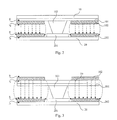
FIG. 1 is a cross-sectional view illustrating a display panel in the prior art;
FIG. 2 is a schematic structural diagram illustrating a display panel of the present disclosure;
FIG. 3 is another schematic structural diagram illustrating a display panel of the present disclosure; and
FIG. 4 is a flow chart illustrating the method for fabricating a display panel of the present disclosure.
DETAILED DESCRIPTION
The present invention and associated general inventive concepts will be further described hereinafter in detail with reference to the accompanying drawings and various exemplary embodiments. One of ordinary skill in the art will appreciate that these exemplary embodiments only constitute a fraction of the possible embodiments encompassed by the present invention and associated general inventive concepts. As such, the scope of the present disclosure is by no means limited to the exemplary embodiments set forth herein.
The present disclosure provides a display panel, a display device, and a method for fabricating a display panel, which can effectively prevent ripples in the display panel and light leakage around the pixel region from occurring in the display panel under a pressure. In certain embodiments, the first substrate comprises a black matrix layer and a first magnetic layer, the second substrate comprises a second magnetic layer which corresponds to the first magnetic layer in position, and the first and second magnetic layers form an attractive magnetic field force between the first and second substrates. The magnetic field force can effectively prevent relative displacement between two substrates of the display panel under a pressure, and can effectively prevent ripples in the display panel and light leakage around the pixel region. Thereby, the display quality may be improved. In the context of the present disclosure, when reference is made to the first and second magnetic layers, the expression “layer” and “film” can be used interchangeably.
Reference numerals in the drawings are explained as follow: 10′—color film substrate, 101′—black matrix layer, 20′—array substrate, 30′—liquid crystal molecule, d-relative displacement, 10—first substrate, 101—black matrix layer, 102—first magnetic layer, 103—spacer, 20—second substrate, 201—thin film transistor, and 202—second magnetic layer.
As shown in FIGS. 2 and 3, in a first embodiment, there is provided a display panel comprising a first substrate 10 and a second substrate 20 which are arranged oppositely. The first substrate 10 comprises a black matrix layer 101 and a first magnetic layer 102. The second substrate 20 comprises a second magnetic layer 202 which corresponds in position to the first magnetic layer 102. The first magnetic layer 102 and the second magnetic layer 202 form an attractive magnetic field force between the first substrate 10 and the second substrate 20.
In certain embodiments, the first substrate can be a color film substrate, and the second substrate can be an array substrate. However, the present disclosure is not limited to this particular arrangement.
Referring to FIG. 2, an exemplary display panel will be described while taking an example in which the first substrate 10 is a color film substrate and the second substrate 20 is an array substrate.
The display panel comprises an array substrate 20 and a color film substrate 10 which are arranged oppositely, a liquid crystal layer which is filled between the array substrate 20 and the color film substrate 10, and a spacer 103 which is formed on the color film substrate 10. The color film substrate 10 comprises a black matrix layer 101 and a first magnetic layer 102. The array substrate 20 comprises a second magnetic layer 202 which corresponds to the first magnetic layer 102 in position. The first magnetic layer 102 and the second magnetic layer 202 may have opposite polarities on their confronting surfaces. In a direction perpendicular to the display panel, the first magnetic layer 102 can correspond to the black matrix layer 101 in position. The first magnetic layer 102 corresponds to the second magnetic layer 202 in position, and the first magnetic layer 102 and the second magnetic layer 202 correspond to the black matrix layer 101 in position, thereby minimizing adverse effect on the light transmittance of the display panel.
The first magnetic layer 102 and the second magnetic layer 202 form an attractive magnetic field force between the first substrate 10 and the second substrate 20, so that upon being arranged oppositely, the first and second substrates can maintain a stable position relative to one another. When the display panel is subjected to a pressure, the relative movement between the array substrate 20 and the color film substrate 10 can be effectively avoided, and a local flow of liquid crystal is avoided. In addition, relative displacement between the array substrate 20 and the color film substrate 10 in a direction parallel with the display panel can be effectively prevented, so that the array substrate and the color film substrate maintain a stable position relative to one another. Namely, the black matrix layer 101 maintains a stable position. This can effectively prevent light leakage around the pixel region, thus greatly improving the display quality. In a region of an alignment layer in the display panel where the rubbing trace is relatively shallow, this effect can be particularly beneficial.
For example in the case wherein the display panel is a touch display panel, when the display panel is touched, two substrates of the display panel can maintain a stable position relative to one another, thus effectively preventing ripples in the display panel and light leakage around the pixel region.
It is noted that the present display panel can be, but not limited to, a TN mode display panel and a FFS (Fringe Field Switching) mode display panel.
In the prior art, when the display panel is under a pressure, relative displacement between the array substrate and the color film substrate in a direction parallel with the plane of the display panel tends to introduce misalignment of the spacer. Thereby, the necessary allowable cell gap of the display panel will not be maintained. In the present display panel, two substrates have a stable relative position when subjected to pressure. This can effectively prevent misalignment between the spacer 103 and a supporting point on the thin film transistor 201, thus ensuring the function of spacer 103 for maintaining the cell gap between the array substrate and the color film substrate. This reduces local flow of liquid crystal in the display panel under a pressure, thus preventing ripples in the display panel and improving display quality.
The material of the first and second magnetic layers can comprise a metal magnetic thin film and a metal oxide magnetic thin film. The metal magnetic thin film can comprise Fe, Co, or Fe—Ni. The metal oxide magnetic thin film can comprise spinel, magneto-plumbite, or garnet type ferrite. The relatively stable magnetic property of the metal oxide magnetic thin film make it an acceptable choice herein. In this manner, it is not only possible to reduce ripples in the display panel and light leakage around the pixel region in the display panel when subjected to a pressure, but also to mitigate the effect on the deflection of liquid crystal.
As shown in FIG. 2, the first magnetic layer 102 can be a top layer of the first substrate 10 on a surface facing the second substrate 20, i.e., one of the layers on the first substrate 10 which is closest to the second substrate 20. The second magnetic layer 202 can be a top layer of the second substrate 20 on a surface facing the first substrate 10, i.e., one of the layers on the second substrate 20 which is closes to the first substrate 10. The first magnetic layer 102 and the second magnetic layer 202 can have opposite polarities on their confronting surfaces. For example, as shown in the left side of FIG. 2, the first magnetic layer 102 can have N polarity on the surface facing the second magnetic layer 202, and the second magnetic layer 202 can have S polarity on the surface facing the first magnetic layer 102. However, the present disclosure is not limited to the case shown in FIG. 2. For example, the first magnetic layer 102 can have S polarity on the surface facing the second magnetic layer 202, and the second magnetic layer 202 can have N polarity on the surface facing the first magnetic layer 102.
As described above, the first and second magnetic layers have opposite polarities on their confronting surfaces, and the first and second magnetic layers are top layers of the first and second substrates, respectively. In other words, the distance between the first and second magnetic layers is relatively small, so that a magnetic field of relatively high intensity is formed between the first and second magnetic layers. This magnetic field of relatively high intensity can reduce the relative displacement between the array substrate and the color film substrate in a direction parallel with the display panel in the display panel when subjected to pressure, thus preventing ripples in the display panel and light leakage around the pixel region.
The first and second magnetic layers can be fabricated by various methods. In certain embodiments, by forming the first magnetic layer on the first substrate as an example, the first magnetic layer can be formed by a vacuum evaporation process. In the vacuum evaporation process, a magnetic material is evaporated onto the first substrate by heating in a vacuum chamber to effect deposition, thus forming the first magnetic layer.
The first magnetic layer can also be formed by an electroplating process. In the electroplating process, the magnetic material and the first substrate are used to act as an anode and a cathode respectively in an electrolyte, and the first magnetic layer is deposited onto the first substrate to form the first magnetic layer.
The first magnetic layer can also be formed by a sputtering process. In the sputtering process, an inert gas filled in a vacuum chamber is ionized, and these ions bombard a target of the magnetic material at a high speed, so that atoms of the magnetic material are sputtered and attached onto the first substrate to form the first magnetic layer.
Alternatively, the first magnetic layer can also be formed by an epitaxial growth process or an electroless plating process. The second magnetic layer may be formed on the second substrate in a similar fashion.
As shown in FIG. 3, in the present display panel, the first magnetic layer 102 can also be a top layer of the first substrate 10 on a surface facing away from the second substrate 20, i.e., one of the layers on the second substrate 20 which is furthest from the first substrate 10. The second magnetic layer 202 can also be a top layer of the second substrate 20 on a surface facing the first substrate 10, i.e., one of the layers on the second substrate 20 which is closes to the first substrate 10. Also, the first magnetic layer 102 and the second magnetic layer 202 have opposite polarities on their confronting surfaces.
Reference is made to an example in which the first magnetic layer 102 and the second magnetic layer 202 have N polarity and S polarity respectively, on their confronting surfaces. When the first substrate 10 and the second substrate 20 are arranged oppositely to form the display panel, the first magnetic layer 102 has N polarity on the surface facing the second magnetic layer 202, and the second magnetic layer 202 has S polarity on the surface facing the first magnetic layer 102. Thus, the first magnetic layer 102 and the second magnetic layer 202 form an attractive magnetic field force between the first substrate 10 and the second substrate 20. The attractive magnetic field force can effectively prevent the relative displacement between the array substrate and the color film substrate when the display panel is subject to a pressure, this reduces any local flow of the liquid crystal, and reduces ripples. In addition, the attractive magnetic field force can reduce the relative displacement between the array substrate and the color film substrate in a direction parallel with the display panel, and prevent light leakage around the pixel region.
In certain embodiments, the first and second magnetic layers can be comprised of similar or identical materials. When the first and second magnetic layers are made from the same material, they can be formed by the same kind of process, so that the fabricating procedure is effectively simplified, and the production cost is reduced.
For example, when the first magnetic layer 102 and the second magnetic layer 202 are FeTe alloy thin films, they can be formed in the following manner. High purity powders of Fe and Te are sintered into a target of FeTe alloy at a temperature of 700° C. The target of FeTe alloy is bombarded by laser at 500° C. in a high vacuum chamber, so that micro-sized alloy particles are sputtered from the target of FeTe alloy and attached onto the substrate. Alternatively, the first and second magnetic layers may be formed by an annealing process at 300° C. in an atmosphere of high purity Ar.
When the first magnetic layer 102 and the second magnetic layer 202 are co-doped ZnO thin films, they can be formed in the following manner. High purity powders of ZnO and Co3O4 are sintered onto a target at high temperature. The target is bombarded by laser at a high temperature of 750° C. in an atmosphere of pure oxygen. The sputtered ZnCoO is deposited onto the substrate to form the respective magnetic layer.
The second magnetic layer 202 is a top layer of the second substrate 20 on a surface facing the first substrate 10. Likewise, the first magnetic layer 102 is a top layer of the first substrate 10 on a surface facing the second substrate 20 (FIG. 2) or a top layer of the first substrate 10 on a surface facing away from the second substrate 20 (FIG. 3). However, the present disclosure is not limited to this.
For example, the first magnetic layer 102 can be a layer which is most away from the second substrate 20, a layer which is closest to the second substrate 20, or any intermediate layer among the stack comprised in the first substrate 10, and the second magnetic layer 202 can also be a layer which is furthest from the first substrate 10, a layer which is closest to the first substrate 10, or any intermediate layer among the stack comprised in the second substrate 20.
Based on the display panel in the above disclosure, the present disclosure further provides a display device, which comprises the display panel as disclosed above.
In embodiments according to the general inventive concepts, when the display panel is subject to a pressure, a relative displacement between two substrates in a direction parallel with the display panel tends not to occur, so that the black matrix layer is fixed in position. Thus, this can reduce ripples in the display panel and reduce light leakage around the pixel region.
The display device can be any product or component with a display function like a mobile phone, tablet computer, TV, monitor, notebook computer, digital photo frame, and navigator. Embodiments for the display device will not be repeated herein for the sake of simplicity.
The present disclosure further provides a method for fabricating a display panel. FIG. 4 is a schematic flow chart illustrating a method for fabricating a display panel of an embodiment. The method comprises steps of:
step 401: forming a black matrix layer and a first magnetic layer on a first substrate;
step 402: forming a second magnetic layer which corresponds in position to the first magnetic layer on a second substrate, wherein the first and second magnetic layers form an attractive magnetic field force between the first and second substrates; and
step 403: arranging the first substrate from step 401 and the second substrate from step 402 oppositely.
It is noted that step 401 can be followed by step 402, step 402 can be followed by step 401, or steps 401, 402 can be performed simultaneously.
A method for fabricating a display panel will be described hereinafter, and the present disclosure is not limited to this method. This method can comprise steps of:
first step: forming a black matrix layer on a plate of a first substrate;
second step: forming a first magnetic layer which corresponds in position to the black matrix layer on the first substrate from the first step;
third step: forming spacers on the first substrate from the second step;
fourth step: forming a plurality of pixel units on a second substrate, wherein the pixel units are arranged in an array, and thin film transistors which correspond to each of the pixel units;
fifth step: forming a second magnetic layer which corresponds in position to the first magnetic layer on the second substrate from the second step, wherein the first and second magnetic layers form an attractive magnetic field force between the first and second substrates; and
sixth step: filling a liquid crystal layer on the first or second substrate from the third or fifth step, and arranging the first and second substrates oppositely with a sealing agent.
In the display panel fabricated by the above method, when the display panel is subjected to a pressure, the first and second magnetic layers form an attractive magnetic field force between the first and second substrates. When the display panel is subject to a pressure, the attractive magnetic field force reduces a relative displacement between two substrates in a direction parallel with the display panel. Namely, the black matrix layer has a stable position. This can effectively prevent ripples in the display panel and light leakage around the pixel region, thus greatly improving the display quality.
Although the present disclosure has been described above with reference to specific embodiments, it should be understood that the limitations of the described embodiments are merely for illustrative purpose and by no means limiting. Instead, the scope of the disclosure is defined by the appended claims rather than by the description, and all variations that fall within the range of the claims are intended to be embraced therein. Thus, other embodiments than the specific ones described above are equally possible within the scope of the appended claims.

Claims (14)

The invention claimed is:
1. A display panel, comprising a first and second substrate which is arranged oppositely, wherein the first substrate comprises a black matrix layer and a first magnetic layer, the second substrate comprises a second magnetic layer which corresponds to the first magnetic layer in position, and the first and second magnetic layers form an attractive magnetic field force between the first and second substrates,
a projection of the first magnetic layer and the second magnetic layer on the first substrate falls within a projection of the black matrix layer on the first substrate.
2. The display panel of claim 1, wherein the first and second magnetic layers have opposite polarities on their confronting surfaces.
3. The display panel of claim 2, wherein the first magnetic layer has N polarity on the surface facing the second magnetic layer, and the second magnetic layer has S polarity on the surface facing the first magnetic layer.
4. The display panel of claim 1, wherein the first magnetic layer is a top layer of the first substrate at a side facing the second substrate, and the second magnetic layer is a top layer of the second substrate at a side facing the first substrate.
5. The display panel of claim 1, wherein the first magnetic layer is a top layer of the first substrate at a side away from the second substrate, and the second magnetic layer is a top layer of the second substrate at a side facing the first substrate.
6. The display panel of claim 5, wherein the first and second magnetic layers have the same material.
7. The display panel of claim 1, wherein the first and second magnetic layers are thin films of a magnetic metal oxide.
8. The display panel of claim 1, wherein the display panel is a touch display panel.
9. A display device, comprising the display panel of claim 1.
10. A method for fabricating a display panel, comprising steps of:
forming a black matrix layer and a first magnetic layer on a first substrate;
forming a second magnetic layer which corresponds to the first magnetic layer in position on a second substrate, wherein the first and second magnetic layers form an attractive magnetic field force between the first and second substrates; and
arranging the first and second substrates oppositely,
wherein a projection of the first magnetic layer and the second magnetic layer on the first substrate falls within a projection of the black matrix layer on the first substrate.
11. The method of claim 10, wherein forming the first and second magnetic layers so that they have opposite polarities on their confronting surfaces.
12. The method of claim 10, wherein the step of forming the first magnetic layer comprises forming the first magnetic layer to have N polarity on the surface facing the second magnetic layer, and the step of forming the second magnetic layer comprises forming the second magnetic layer to have S polarity on the surface facing the first magnetic layer.
13. The method of claim 11, wherein the step of forming the first magnetic layer comprises forming the first magnetic layer as a top layer of the first substrate at a side facing the second substrate, and the step of forming the second magnetic layer comprises forming the second magnetic layer as a top layer of the second substrate at a side facing the first substrate.
14. The method of claim 11, wherein the step of forming the first magnetic layer comprises forming the first magnetic layer as a top layer of the first substrate at a side away from the second substrate, and the step of forming the second magnetic layer comprises forming the second magnetic layer as a top layer of the second substrate at a side facing the first substrate.
US14/500,620 2014-05-30 2014-09-29 Display panel comprising first and second magenetic layers, display device comprising the same, and method for fabricating the display panel Active 2034-10-04 US9535281B2 (en)

Applications Claiming Priority (3)

Application Number Priority Date Filing Date Title
CN201410240894.1 2014-05-30
CN201410240894 2014-05-30
CN201410240894.1A CN104020594B (en) 2014-05-30 2014-05-30 A kind of manufacture method of display floater, display device and display floater

Publications (2)

Publication Number Publication Date
US20150346544A1 US20150346544A1 (en) 2015-12-03
US9535281B2 true US9535281B2 (en) 2017-01-03

Family

ID=51437430

Family Applications (1)

Application Number Title Priority Date Filing Date
US14/500,620 Active 2034-10-04 US9535281B2 (en) 2014-05-30 2014-09-29 Display panel comprising first and second magenetic layers, display device comprising the same, and method for fabricating the display panel

Country Status (2)

Country Link
US (1) US9535281B2 (en)
CN (1) CN104020594B (en)

Families Citing this family (12)

* Cited by examiner, † Cited by third party
Publication number Priority date Publication date Assignee Title
CN104793385B (en) * 2015-04-23 2018-01-19 京东方科技集团股份有限公司 Stripping means, display base plate and the display device of ultra-thin substrate
KR102496918B1 (en) * 2015-11-27 2023-02-08 삼성디스플레이 주식회사 Display device
KR20170068687A (en) * 2015-12-09 2017-06-20 삼성디스플레이 주식회사 Liquid crystal display and method for manufacturing the same
CN105741682B (en) * 2016-05-13 2019-06-07 京东方科技集团股份有限公司 A kind of display panel and display device
CN106950739A (en) * 2017-04-28 2017-07-14 京东方科技集团股份有限公司 A kind of display panel, the alignment method of display panel, alignment device
CN107170910A (en) * 2017-05-25 2017-09-15 京东方科技集团股份有限公司 The preparation method of display base plate, display base plate motherboard
US10627678B2 (en) 2017-12-13 2020-04-21 Boe Technology Group Co., Ltd. Display apparatus having transparent magnetic layer, and fabricating method thereof
CN109493737A (en) * 2018-12-14 2019-03-19 云谷(固安)科技有限公司 Flexible die group, flexible display panels and flexible display apparatus
CN112271200B (en) * 2020-10-26 2022-07-12 京东方科技集团股份有限公司 Display panel, preparation method thereof and display device
CN113870710B (en) * 2021-09-29 2023-08-22 上海天马微电子有限公司 Flexible display device
CN114241921B (en) * 2021-12-30 2023-11-14 合肥维信诺科技有限公司 Flexible display module and flexible display device
CN114895491B (en) * 2022-06-08 2023-11-21 厦门天马微电子有限公司 Display panel and display device

Citations (6)

* Cited by examiner, † Cited by third party
Publication number Priority date Publication date Assignee Title
JPH0926580A (en) 1995-07-11 1997-01-28 Toshiba Electron Eng Corp Liquid crystal display device
US20080105550A1 (en) * 2003-10-06 2008-05-08 Kabushiki Kaisha Pilot Corportion (Also Trading As Pilot Corporation Magnetic Migration and Reversal Display Panel and Magnetic Migration and Reversal Display Method
US20090079929A1 (en) * 2007-09-20 2009-03-26 National Chiao Tung University Method of alignments of liquid crystal employing magnetic thin films
US20100079718A1 (en) * 2008-10-01 2010-04-01 Hitachi Displays, Ltd. Liquid crystal display device
CN103293777A (en) 2013-05-24 2013-09-11 京东方科技集团股份有限公司 Display panel, display device applying same and display panel manufacturing method
CN103792722A (en) 2014-01-22 2014-05-14 京东方科技集团股份有限公司 Display device, display panel and manufacturing method thereof

Family Cites Families (1)

* Cited by examiner, † Cited by third party
Publication number Priority date Publication date Assignee Title
CN202486472U (en) * 2011-12-05 2012-10-10 京东方科技集团股份有限公司 Liquid crystal display (LCD) panel and display device

Patent Citations (6)

* Cited by examiner, † Cited by third party
Publication number Priority date Publication date Assignee Title
JPH0926580A (en) 1995-07-11 1997-01-28 Toshiba Electron Eng Corp Liquid crystal display device
US20080105550A1 (en) * 2003-10-06 2008-05-08 Kabushiki Kaisha Pilot Corportion (Also Trading As Pilot Corporation Magnetic Migration and Reversal Display Panel and Magnetic Migration and Reversal Display Method
US20090079929A1 (en) * 2007-09-20 2009-03-26 National Chiao Tung University Method of alignments of liquid crystal employing magnetic thin films
US20100079718A1 (en) * 2008-10-01 2010-04-01 Hitachi Displays, Ltd. Liquid crystal display device
CN103293777A (en) 2013-05-24 2013-09-11 京东方科技集团股份有限公司 Display panel, display device applying same and display panel manufacturing method
CN103792722A (en) 2014-01-22 2014-05-14 京东方科技集团股份有限公司 Display device, display panel and manufacturing method thereof

Non-Patent Citations (1)

* Cited by examiner, † Cited by third party
Title
Office action from Chinese Application No. 201410240894.1 dated Mar. 2, 2016.

Also Published As

Publication number Publication date
CN104020594B (en) 2016-08-31
CN104020594A (en) 2014-09-03
US20150346544A1 (en) 2015-12-03

Similar Documents

Publication Publication Date Title
US9535281B2 (en) Display panel comprising first and second magenetic layers, display device comprising the same, and method for fabricating the display panel
CN102707504B (en) Liquid crystal panel and preparation method thereof, display device
JP5285729B2 (en) Liquid crystal display
US9698369B2 (en) Display panel and manufacturing method thereof and display device
US10551686B2 (en) Liquid crystal display device and mother substrate
US20120199477A1 (en) Film forming apparatus
US9589991B2 (en) Thin-film transistor, manufacturing method thereof, display substrate and display device
US20140078438A1 (en) Tft array substrate and manufacturing method thereof, and display apparatus
EP3171405B1 (en) Display substrate and manufacturing method therefor, and display apparatus
US20210165291A1 (en) Display panel and method for manufacturing same
TWI627300B (en) Methods for coating a substrate and coater
TWI630658B (en) Transparent conductive film and method of manufacturing same
US20170235177A1 (en) Curved display panel and electronic apparatus
US20200251499A1 (en) Display Panel and Method for Manufacturing Thereof
US9134559B2 (en) Method for preparing conducting film on ultra-thin glass substrate, LCD substrate, liquid crystal panel and LCD device
JP5352537B2 (en) Deposition equipment
US20160248049A1 (en) Deposition apparatus
CN104765216B (en) Array base palte and preparation method thereof and display device
JP5447240B2 (en) Magnetron sputtering apparatus and method for producing transparent conductive film
CN105039917B (en) A kind of glass lens and preparation method thereof with sapphire surface layer
US20170044659A1 (en) Magnetron sputtering device and method using the same
CN107367882B (en) Liquid crystal lens structure, liquid crystal lens forming method, display panel and device
CN103995395B (en) A kind of LCDs and manufacture method
CN102677006A (en) Transparent amorphous oxide semiconductor sputtering target
CN103744227A (en) Color film substrate, manufacturing method and display device

Legal Events

Date Code Title Description
AS Assignment

Owner name: BOE TECHNOLOGY GROUP CO., LTD., CHINA

Free format text: ASSIGNMENT OF ASSIGNORS INTEREST;ASSIGNORS:WU, JUN;ZHAN, HONGMING;TIAN, CHAO;SIGNING DATES FROM 20140919 TO 20140923;REEL/FRAME:034194/0527

Owner name: BEIJING BOE DISPLAY TECHNOLOGY CO., LTD., CHINA

Free format text: ASSIGNMENT OF ASSIGNORS INTEREST;ASSIGNORS:WU, JUN;ZHAN, HONGMING;TIAN, CHAO;SIGNING DATES FROM 20140919 TO 20140923;REEL/FRAME:034194/0527

STCF Information on status: patent grant

Free format text: PATENTED CASE

MAFP Maintenance fee payment

Free format text: PAYMENT OF MAINTENANCE FEE, 4TH YEAR, LARGE ENTITY (ORIGINAL EVENT CODE: M1551); ENTITY STATUS OF PATENT OWNER: LARGE ENTITY

Year of fee payment: 4

MAFP Maintenance fee payment

Free format text: PAYMENT OF MAINTENANCE FEE, 8TH YEAR, LARGE ENTITY (ORIGINAL EVENT CODE: M1552); ENTITY STATUS OF PATENT OWNER: LARGE ENTITY

Year of fee payment: 8