US9530867B2 - Method for manufacturing a super-junction structures having implanted regions surrounding an N epitaxial layer in deep trench - Google Patents
Method for manufacturing a super-junction structures having implanted regions surrounding an N epitaxial layer in deep trench Download PDFInfo
- Publication number
- US9530867B2 US9530867B2 US14/799,878 US201514799878A US9530867B2 US 9530867 B2 US9530867 B2 US 9530867B2 US 201514799878 A US201514799878 A US 201514799878A US 9530867 B2 US9530867 B2 US 9530867B2
- Authority
- US
- United States
- Prior art keywords
- deep trench
- epitaxial layer
- conductivity type
- mask
- layer
- Prior art date
- Legal status (The legal status is an assumption and is not a legal conclusion. Google has not performed a legal analysis and makes no representation as to the accuracy of the status listed.)
- Active
Links
- 238000000034 method Methods 0.000 title claims abstract description 11
- 238000004519 manufacturing process Methods 0.000 title claims abstract description 8
- 239000000758 substrate Substances 0.000 claims abstract description 19
- 239000002019 doping agent Substances 0.000 claims abstract description 15
- 238000005468 ion implantation Methods 0.000 claims abstract description 14
- XUIMIQQOPSSXEZ-UHFFFAOYSA-N Silicon Chemical compound [Si] XUIMIQQOPSSXEZ-UHFFFAOYSA-N 0.000 claims abstract description 9
- 238000009792 diffusion process Methods 0.000 claims abstract description 9
- 229910052710 silicon Inorganic materials 0.000 claims abstract description 9
- 239000010703 silicon Substances 0.000 claims abstract description 9
- 239000010410 layer Substances 0.000 claims description 77
- 210000000746 body region Anatomy 0.000 claims description 17
- 239000011229 interlayer Substances 0.000 claims description 7
- 238000005530 etching Methods 0.000 claims description 6
- 229910021420 polycrystalline silicon Inorganic materials 0.000 claims description 4
- 238000000151 deposition Methods 0.000 claims 2
- 229910052751 metal Inorganic materials 0.000 description 18
- 239000002184 metal Substances 0.000 description 18
- 230000015572 biosynthetic process Effects 0.000 description 7
- 230000000149 penetrating effect Effects 0.000 description 5
- 239000004065 semiconductor Substances 0.000 description 5
- 229910052698 phosphorus Inorganic materials 0.000 description 4
- 230000015556 catabolic process Effects 0.000 description 3
- OAICVXFJPJFONN-UHFFFAOYSA-N Phosphorus Chemical compound [P] OAICVXFJPJFONN-UHFFFAOYSA-N 0.000 description 2
- 239000011521 glass Substances 0.000 description 2
- 238000012986 modification Methods 0.000 description 2
- 230000004048 modification Effects 0.000 description 2
- 230000003647 oxidation Effects 0.000 description 2
- 238000007254 oxidation reaction Methods 0.000 description 2
- 239000011574 phosphorus Substances 0.000 description 2
- 238000004151 rapid thermal annealing Methods 0.000 description 2
- WFKWXMTUELFFGS-UHFFFAOYSA-N tungsten Chemical compound [W] WFKWXMTUELFFGS-UHFFFAOYSA-N 0.000 description 2
- 229910052721 tungsten Inorganic materials 0.000 description 2
- 239000010937 tungsten Substances 0.000 description 2
- 229910000838 Al alloy Inorganic materials 0.000 description 1
- ZOXJGFHDIHLPTG-UHFFFAOYSA-N Boron Chemical compound [B] ZOXJGFHDIHLPTG-UHFFFAOYSA-N 0.000 description 1
- MXSJNBRAMXILSE-UHFFFAOYSA-N [Si].[P].[B] Chemical compound [Si].[P].[B] MXSJNBRAMXILSE-UHFFFAOYSA-N 0.000 description 1
- 230000004888 barrier function Effects 0.000 description 1
- 229910052796 boron Inorganic materials 0.000 description 1
- 230000005669 field effect Effects 0.000 description 1
- 238000000227 grinding Methods 0.000 description 1
- 231100001261 hazardous Toxicity 0.000 description 1
- 238000002513 implantation Methods 0.000 description 1
- 239000000463 material Substances 0.000 description 1
- 229910044991 metal oxide Inorganic materials 0.000 description 1
- 150000004706 metal oxides Chemical class 0.000 description 1
- 239000011800 void material Substances 0.000 description 1
Images


Classifications
-
- H—ELECTRICITY
- H01—ELECTRIC ELEMENTS
- H01L—SEMICONDUCTOR DEVICES NOT COVERED BY CLASS H10
- H01L29/00—Semiconductor devices adapted for rectifying, amplifying, oscillating or switching, or capacitors or resistors with at least one potential-jump barrier or surface barrier, e.g. PN junction depletion layer or carrier concentration layer; Details of semiconductor bodies or of electrodes thereof ; Multistep manufacturing processes therefor
- H01L29/66—Types of semiconductor device ; Multistep manufacturing processes therefor
- H01L29/66007—Multistep manufacturing processes
- H01L29/66075—Multistep manufacturing processes of devices having semiconductor bodies comprising group 14 or group 13/15 materials
- H01L29/66227—Multistep manufacturing processes of devices having semiconductor bodies comprising group 14 or group 13/15 materials the devices being controllable only by the electric current supplied or the electric potential applied, to an electrode which does not carry the current to be rectified, amplified or switched, e.g. three-terminal devices
- H01L29/66409—Unipolar field-effect transistors
- H01L29/66477—Unipolar field-effect transistors with an insulated gate, i.e. MISFET
- H01L29/66674—DMOS transistors, i.e. MISFETs with a channel accommodating body or base region adjoining a drain drift region
- H01L29/66712—Vertical DMOS transistors, i.e. VDMOS transistors
- H01L29/66734—Vertical DMOS transistors, i.e. VDMOS transistors with a step of recessing the gate electrode, e.g. to form a trench gate electrode
-
- H—ELECTRICITY
- H01—ELECTRIC ELEMENTS
- H01L—SEMICONDUCTOR DEVICES NOT COVERED BY CLASS H10
- H01L21/00—Processes or apparatus adapted for the manufacture or treatment of semiconductor or solid state devices or of parts thereof
- H01L21/02—Manufacture or treatment of semiconductor devices or of parts thereof
- H01L21/04—Manufacture or treatment of semiconductor devices or of parts thereof the devices having at least one potential-jump barrier or surface barrier, e.g. PN junction, depletion layer or carrier concentration layer
- H01L21/18—Manufacture or treatment of semiconductor devices or of parts thereof the devices having at least one potential-jump barrier or surface barrier, e.g. PN junction, depletion layer or carrier concentration layer the devices having semiconductor bodies comprising elements of Group IV of the Periodic System or AIIIBV compounds with or without impurities, e.g. doping materials
- H01L21/28—Manufacture of electrodes on semiconductor bodies using processes or apparatus not provided for in groups H01L21/20 - H01L21/268
- H01L21/28008—Making conductor-insulator-semiconductor electrodes
- H01L21/28017—Making conductor-insulator-semiconductor electrodes the insulator being formed after the semiconductor body, the semiconductor being silicon
- H01L21/28026—Making conductor-insulator-semiconductor electrodes the insulator being formed after the semiconductor body, the semiconductor being silicon characterised by the conductor
- H01L21/28035—Making conductor-insulator-semiconductor electrodes the insulator being formed after the semiconductor body, the semiconductor being silicon characterised by the conductor the final conductor layer next to the insulator being silicon, e.g. polysilicon, with or without impurities
-
- H—ELECTRICITY
- H01—ELECTRIC ELEMENTS
- H01L—SEMICONDUCTOR DEVICES NOT COVERED BY CLASS H10
- H01L21/00—Processes or apparatus adapted for the manufacture or treatment of semiconductor or solid state devices or of parts thereof
- H01L21/02—Manufacture or treatment of semiconductor devices or of parts thereof
- H01L21/04—Manufacture or treatment of semiconductor devices or of parts thereof the devices having at least one potential-jump barrier or surface barrier, e.g. PN junction, depletion layer or carrier concentration layer
- H01L21/18—Manufacture or treatment of semiconductor devices or of parts thereof the devices having at least one potential-jump barrier or surface barrier, e.g. PN junction, depletion layer or carrier concentration layer the devices having semiconductor bodies comprising elements of Group IV of the Periodic System or AIIIBV compounds with or without impurities, e.g. doping materials
- H01L21/30—Treatment of semiconductor bodies using processes or apparatus not provided for in groups H01L21/20 - H01L21/26
- H01L21/302—Treatment of semiconductor bodies using processes or apparatus not provided for in groups H01L21/20 - H01L21/26 to change their surface-physical characteristics or shape, e.g. etching, polishing, cutting
- H01L21/306—Chemical or electrical treatment, e.g. electrolytic etching
- H01L21/3065—Plasma etching; Reactive-ion etching
-
- H—ELECTRICITY
- H01—ELECTRIC ELEMENTS
- H01L—SEMICONDUCTOR DEVICES NOT COVERED BY CLASS H10
- H01L21/00—Processes or apparatus adapted for the manufacture or treatment of semiconductor or solid state devices or of parts thereof
- H01L21/02—Manufacture or treatment of semiconductor devices or of parts thereof
- H01L21/04—Manufacture or treatment of semiconductor devices or of parts thereof the devices having at least one potential-jump barrier or surface barrier, e.g. PN junction, depletion layer or carrier concentration layer
- H01L21/18—Manufacture or treatment of semiconductor devices or of parts thereof the devices having at least one potential-jump barrier or surface barrier, e.g. PN junction, depletion layer or carrier concentration layer the devices having semiconductor bodies comprising elements of Group IV of the Periodic System or AIIIBV compounds with or without impurities, e.g. doping materials
- H01L21/30—Treatment of semiconductor bodies using processes or apparatus not provided for in groups H01L21/20 - H01L21/26
- H01L21/31—Treatment of semiconductor bodies using processes or apparatus not provided for in groups H01L21/20 - H01L21/26 to form insulating layers thereon, e.g. for masking or by using photolithographic techniques; After treatment of these layers; Selection of materials for these layers
- H01L21/3205—Deposition of non-insulating-, e.g. conductive- or resistive-, layers on insulating layers; After-treatment of these layers
- H01L21/321—After treatment
- H01L21/32115—Planarisation
- H01L21/3212—Planarisation by chemical mechanical polishing [CMP]
-
- H—ELECTRICITY
- H01—ELECTRIC ELEMENTS
- H01L—SEMICONDUCTOR DEVICES NOT COVERED BY CLASS H10
- H01L21/00—Processes or apparatus adapted for the manufacture or treatment of semiconductor or solid state devices or of parts thereof
- H01L21/02—Manufacture or treatment of semiconductor devices or of parts thereof
- H01L21/04—Manufacture or treatment of semiconductor devices or of parts thereof the devices having at least one potential-jump barrier or surface barrier, e.g. PN junction, depletion layer or carrier concentration layer
- H01L21/18—Manufacture or treatment of semiconductor devices or of parts thereof the devices having at least one potential-jump barrier or surface barrier, e.g. PN junction, depletion layer or carrier concentration layer the devices having semiconductor bodies comprising elements of Group IV of the Periodic System or AIIIBV compounds with or without impurities, e.g. doping materials
- H01L21/30—Treatment of semiconductor bodies using processes or apparatus not provided for in groups H01L21/20 - H01L21/26
- H01L21/31—Treatment of semiconductor bodies using processes or apparatus not provided for in groups H01L21/20 - H01L21/26 to form insulating layers thereon, e.g. for masking or by using photolithographic techniques; After treatment of these layers; Selection of materials for these layers
- H01L21/3205—Deposition of non-insulating-, e.g. conductive- or resistive-, layers on insulating layers; After-treatment of these layers
- H01L21/321—After treatment
- H01L21/3213—Physical or chemical etching of the layers, e.g. to produce a patterned layer from a pre-deposited extensive layer
- H01L21/32133—Physical or chemical etching of the layers, e.g. to produce a patterned layer from a pre-deposited extensive layer by chemical means only
- H01L21/32135—Physical or chemical etching of the layers, e.g. to produce a patterned layer from a pre-deposited extensive layer by chemical means only by vapour etching only
- H01L21/32136—Physical or chemical etching of the layers, e.g. to produce a patterned layer from a pre-deposited extensive layer by chemical means only by vapour etching only using plasmas
- H01L21/32137—Physical or chemical etching of the layers, e.g. to produce a patterned layer from a pre-deposited extensive layer by chemical means only by vapour etching only using plasmas of silicon-containing layers
-
- H—ELECTRICITY
- H01—ELECTRIC ELEMENTS
- H01L—SEMICONDUCTOR DEVICES NOT COVERED BY CLASS H10
- H01L29/00—Semiconductor devices adapted for rectifying, amplifying, oscillating or switching, or capacitors or resistors with at least one potential-jump barrier or surface barrier, e.g. PN junction depletion layer or carrier concentration layer; Details of semiconductor bodies or of electrodes thereof ; Multistep manufacturing processes therefor
- H01L29/02—Semiconductor bodies ; Multistep manufacturing processes therefor
- H01L29/06—Semiconductor bodies ; Multistep manufacturing processes therefor characterised by their shape; characterised by the shapes, relative sizes, or dispositions of the semiconductor regions ; characterised by the concentration or distribution of impurities within semiconductor regions
- H01L29/0603—Semiconductor bodies ; Multistep manufacturing processes therefor characterised by their shape; characterised by the shapes, relative sizes, or dispositions of the semiconductor regions ; characterised by the concentration or distribution of impurities within semiconductor regions characterised by particular constructional design considerations, e.g. for preventing surface leakage, for controlling electric field concentration or for internal isolations regions
- H01L29/0607—Semiconductor bodies ; Multistep manufacturing processes therefor characterised by their shape; characterised by the shapes, relative sizes, or dispositions of the semiconductor regions ; characterised by the concentration or distribution of impurities within semiconductor regions characterised by particular constructional design considerations, e.g. for preventing surface leakage, for controlling electric field concentration or for internal isolations regions for preventing surface leakage or controlling electric field concentration
- H01L29/0611—Semiconductor bodies ; Multistep manufacturing processes therefor characterised by their shape; characterised by the shapes, relative sizes, or dispositions of the semiconductor regions ; characterised by the concentration or distribution of impurities within semiconductor regions characterised by particular constructional design considerations, e.g. for preventing surface leakage, for controlling electric field concentration or for internal isolations regions for preventing surface leakage or controlling electric field concentration for increasing or controlling the breakdown voltage of reverse biased devices
- H01L29/0615—Semiconductor bodies ; Multistep manufacturing processes therefor characterised by their shape; characterised by the shapes, relative sizes, or dispositions of the semiconductor regions ; characterised by the concentration or distribution of impurities within semiconductor regions characterised by particular constructional design considerations, e.g. for preventing surface leakage, for controlling electric field concentration or for internal isolations regions for preventing surface leakage or controlling electric field concentration for increasing or controlling the breakdown voltage of reverse biased devices by the doping profile or the shape or the arrangement of the PN junction, or with supplementary regions, e.g. junction termination extension [JTE]
- H01L29/0619—Semiconductor bodies ; Multistep manufacturing processes therefor characterised by their shape; characterised by the shapes, relative sizes, or dispositions of the semiconductor regions ; characterised by the concentration or distribution of impurities within semiconductor regions characterised by particular constructional design considerations, e.g. for preventing surface leakage, for controlling electric field concentration or for internal isolations regions for preventing surface leakage or controlling electric field concentration for increasing or controlling the breakdown voltage of reverse biased devices by the doping profile or the shape or the arrangement of the PN junction, or with supplementary regions, e.g. junction termination extension [JTE] with a supplementary region doped oppositely to or in rectifying contact with the semiconductor containing or contacting region, e.g. guard rings with PN or Schottky junction
-
- H—ELECTRICITY
- H01—ELECTRIC ELEMENTS
- H01L—SEMICONDUCTOR DEVICES NOT COVERED BY CLASS H10
- H01L29/00—Semiconductor devices adapted for rectifying, amplifying, oscillating or switching, or capacitors or resistors with at least one potential-jump barrier or surface barrier, e.g. PN junction depletion layer or carrier concentration layer; Details of semiconductor bodies or of electrodes thereof ; Multistep manufacturing processes therefor
- H01L29/02—Semiconductor bodies ; Multistep manufacturing processes therefor
- H01L29/06—Semiconductor bodies ; Multistep manufacturing processes therefor characterised by their shape; characterised by the shapes, relative sizes, or dispositions of the semiconductor regions ; characterised by the concentration or distribution of impurities within semiconductor regions
- H01L29/0603—Semiconductor bodies ; Multistep manufacturing processes therefor characterised by their shape; characterised by the shapes, relative sizes, or dispositions of the semiconductor regions ; characterised by the concentration or distribution of impurities within semiconductor regions characterised by particular constructional design considerations, e.g. for preventing surface leakage, for controlling electric field concentration or for internal isolations regions
- H01L29/0607—Semiconductor bodies ; Multistep manufacturing processes therefor characterised by their shape; characterised by the shapes, relative sizes, or dispositions of the semiconductor regions ; characterised by the concentration or distribution of impurities within semiconductor regions characterised by particular constructional design considerations, e.g. for preventing surface leakage, for controlling electric field concentration or for internal isolations regions for preventing surface leakage or controlling electric field concentration
- H01L29/0611—Semiconductor bodies ; Multistep manufacturing processes therefor characterised by their shape; characterised by the shapes, relative sizes, or dispositions of the semiconductor regions ; characterised by the concentration or distribution of impurities within semiconductor regions characterised by particular constructional design considerations, e.g. for preventing surface leakage, for controlling electric field concentration or for internal isolations regions for preventing surface leakage or controlling electric field concentration for increasing or controlling the breakdown voltage of reverse biased devices
- H01L29/0615—Semiconductor bodies ; Multistep manufacturing processes therefor characterised by their shape; characterised by the shapes, relative sizes, or dispositions of the semiconductor regions ; characterised by the concentration or distribution of impurities within semiconductor regions characterised by particular constructional design considerations, e.g. for preventing surface leakage, for controlling electric field concentration or for internal isolations regions for preventing surface leakage or controlling electric field concentration for increasing or controlling the breakdown voltage of reverse biased devices by the doping profile or the shape or the arrangement of the PN junction, or with supplementary regions, e.g. junction termination extension [JTE]
- H01L29/063—Reduced surface field [RESURF] pn-junction structures
- H01L29/0634—Multiple reduced surface field (multi-RESURF) structures, e.g. double RESURF, charge compensation, cool, superjunction (SJ), 3D-RESURF, composite buffer (CB) structures
-
- H—ELECTRICITY
- H01—ELECTRIC ELEMENTS
- H01L—SEMICONDUCTOR DEVICES NOT COVERED BY CLASS H10
- H01L29/00—Semiconductor devices adapted for rectifying, amplifying, oscillating or switching, or capacitors or resistors with at least one potential-jump barrier or surface barrier, e.g. PN junction depletion layer or carrier concentration layer; Details of semiconductor bodies or of electrodes thereof ; Multistep manufacturing processes therefor
- H01L29/66—Types of semiconductor device ; Multistep manufacturing processes therefor
- H01L29/68—Types of semiconductor device ; Multistep manufacturing processes therefor controllable by only the electric current supplied, or only the electric potential applied, to an electrode which does not carry the current to be rectified, amplified or switched
- H01L29/76—Unipolar devices, e.g. field effect transistors
- H01L29/772—Field effect transistors
- H01L29/78—Field effect transistors with field effect produced by an insulated gate
- H01L29/7801—DMOS transistors, i.e. MISFETs with a channel accommodating body or base region adjoining a drain drift region
- H01L29/7802—Vertical DMOS transistors, i.e. VDMOS transistors
- H01L29/7811—Vertical DMOS transistors, i.e. VDMOS transistors with an edge termination structure
-
- H—ELECTRICITY
- H01—ELECTRIC ELEMENTS
- H01L—SEMICONDUCTOR DEVICES NOT COVERED BY CLASS H10
- H01L29/00—Semiconductor devices adapted for rectifying, amplifying, oscillating or switching, or capacitors or resistors with at least one potential-jump barrier or surface barrier, e.g. PN junction depletion layer or carrier concentration layer; Details of semiconductor bodies or of electrodes thereof ; Multistep manufacturing processes therefor
- H01L29/66—Types of semiconductor device ; Multistep manufacturing processes therefor
- H01L29/68—Types of semiconductor device ; Multistep manufacturing processes therefor controllable by only the electric current supplied, or only the electric potential applied, to an electrode which does not carry the current to be rectified, amplified or switched
- H01L29/76—Unipolar devices, e.g. field effect transistors
- H01L29/772—Field effect transistors
- H01L29/78—Field effect transistors with field effect produced by an insulated gate
- H01L29/7801—DMOS transistors, i.e. MISFETs with a channel accommodating body or base region adjoining a drain drift region
- H01L29/7802—Vertical DMOS transistors, i.e. VDMOS transistors
- H01L29/7813—Vertical DMOS transistors, i.e. VDMOS transistors with trench gate electrode, e.g. UMOS transistors
-
- H—ELECTRICITY
- H01—ELECTRIC ELEMENTS
- H01L—SEMICONDUCTOR DEVICES NOT COVERED BY CLASS H10
- H01L21/00—Processes or apparatus adapted for the manufacture or treatment of semiconductor or solid state devices or of parts thereof
- H01L21/02—Manufacture or treatment of semiconductor devices or of parts thereof
- H01L21/04—Manufacture or treatment of semiconductor devices or of parts thereof the devices having at least one potential-jump barrier or surface barrier, e.g. PN junction, depletion layer or carrier concentration layer
- H01L21/18—Manufacture or treatment of semiconductor devices or of parts thereof the devices having at least one potential-jump barrier or surface barrier, e.g. PN junction, depletion layer or carrier concentration layer the devices having semiconductor bodies comprising elements of Group IV of the Periodic System or AIIIBV compounds with or without impurities, e.g. doping materials
- H01L21/26—Bombardment with radiation
- H01L21/263—Bombardment with radiation with high-energy radiation
- H01L21/265—Bombardment with radiation with high-energy radiation producing ion implantation
- H01L21/26586—Bombardment with radiation with high-energy radiation producing ion implantation characterised by the angle between the ion beam and the crystal planes or the main crystal surface
-
- H—ELECTRICITY
- H01—ELECTRIC ELEMENTS
- H01L—SEMICONDUCTOR DEVICES NOT COVERED BY CLASS H10
- H01L29/00—Semiconductor devices adapted for rectifying, amplifying, oscillating or switching, or capacitors or resistors with at least one potential-jump barrier or surface barrier, e.g. PN junction depletion layer or carrier concentration layer; Details of semiconductor bodies or of electrodes thereof ; Multistep manufacturing processes therefor
- H01L29/02—Semiconductor bodies ; Multistep manufacturing processes therefor
- H01L29/06—Semiconductor bodies ; Multistep manufacturing processes therefor characterised by their shape; characterised by the shapes, relative sizes, or dispositions of the semiconductor regions ; characterised by the concentration or distribution of impurities within semiconductor regions
- H01L29/10—Semiconductor bodies ; Multistep manufacturing processes therefor characterised by their shape; characterised by the shapes, relative sizes, or dispositions of the semiconductor regions ; characterised by the concentration or distribution of impurities within semiconductor regions with semiconductor regions connected to an electrode not carrying current to be rectified, amplified or switched and such electrode being part of a semiconductor device which comprises three or more electrodes
- H01L29/1095—Body region, i.e. base region, of DMOS transistors or IGBTs
-
- H—ELECTRICITY
- H01—ELECTRIC ELEMENTS
- H01L—SEMICONDUCTOR DEVICES NOT COVERED BY CLASS H10
- H01L29/00—Semiconductor devices adapted for rectifying, amplifying, oscillating or switching, or capacitors or resistors with at least one potential-jump barrier or surface barrier, e.g. PN junction depletion layer or carrier concentration layer; Details of semiconductor bodies or of electrodes thereof ; Multistep manufacturing processes therefor
- H01L29/40—Electrodes ; Multistep manufacturing processes therefor
- H01L29/41—Electrodes ; Multistep manufacturing processes therefor characterised by their shape, relative sizes or dispositions
- H01L29/417—Electrodes ; Multistep manufacturing processes therefor characterised by their shape, relative sizes or dispositions carrying the current to be rectified, amplified or switched
- H01L29/41725—Source or drain electrodes for field effect devices
- H01L29/41766—Source or drain electrodes for field effect devices with at least part of the source or drain electrode having contact below the semiconductor surface, e.g. the source or drain electrode formed at least partially in a groove or with inclusions of conductor inside the semiconductor
-
- H—ELECTRICITY
- H01—ELECTRIC ELEMENTS
- H01L—SEMICONDUCTOR DEVICES NOT COVERED BY CLASS H10
- H01L29/00—Semiconductor devices adapted for rectifying, amplifying, oscillating or switching, or capacitors or resistors with at least one potential-jump barrier or surface barrier, e.g. PN junction depletion layer or carrier concentration layer; Details of semiconductor bodies or of electrodes thereof ; Multistep manufacturing processes therefor
- H01L29/66—Types of semiconductor device ; Multistep manufacturing processes therefor
- H01L29/66007—Multistep manufacturing processes
- H01L29/66075—Multistep manufacturing processes of devices having semiconductor bodies comprising group 14 or group 13/15 materials
- H01L29/66227—Multistep manufacturing processes of devices having semiconductor bodies comprising group 14 or group 13/15 materials the devices being controllable only by the electric current supplied or the electric potential applied, to an electrode which does not carry the current to be rectified, amplified or switched, e.g. three-terminal devices
- H01L29/66409—Unipolar field-effect transistors
- H01L29/66477—Unipolar field-effect transistors with an insulated gate, i.e. MISFET
- H01L29/66674—DMOS transistors, i.e. MISFETs with a channel accommodating body or base region adjoining a drain drift region
- H01L29/66712—Vertical DMOS transistors, i.e. VDMOS transistors
- H01L29/66727—Vertical DMOS transistors, i.e. VDMOS transistors with a step of recessing the source electrode
-
- H—ELECTRICITY
- H01—ELECTRIC ELEMENTS
- H01L—SEMICONDUCTOR DEVICES NOT COVERED BY CLASS H10
- H01L29/00—Semiconductor devices adapted for rectifying, amplifying, oscillating or switching, or capacitors or resistors with at least one potential-jump barrier or surface barrier, e.g. PN junction depletion layer or carrier concentration layer; Details of semiconductor bodies or of electrodes thereof ; Multistep manufacturing processes therefor
- H01L29/66—Types of semiconductor device ; Multistep manufacturing processes therefor
- H01L29/86—Types of semiconductor device ; Multistep manufacturing processes therefor controllable only by variation of the electric current supplied, or only the electric potential applied, to one or more of the electrodes carrying the current to be rectified, amplified, oscillated or switched
- H01L29/861—Diodes
- H01L29/872—Schottky diodes
Definitions
- This invention relates generally to the cell structure, device configuration and fabrication process of power semiconductor devices. More particularly, this invention relates to a novel and improved cell structure, device configuration and improved process of super-junction structures.
- Super-junction structures are more and more attractive due to higher breakdown voltage and lower specific Rds (drain-source resistance).
- a super-junction structure is implemented by p type column structures and n type column structures arranged in parallel and connecting to each other onto a heavily doped substrate, however, the manufacturing yield is not stable because the super-junction structure is very sensitive to the fabrication processes and conditions such as: the p type column structures and n type column structures dopant re-diffusion issue induced by subsequent thermal processes; trapped charges within the column structures, etc. . . . . All that will cause a hazardous condition of charges imbalance to the super-junction structure. More specifically, these undesired influences become more pronounced with a narrower column structure width for a lower bias voltage ranging under 200V.
- U.S. Pat. No. 7,601,597 disclosed a method to avoid the aforementioned p type column structure and n type structure dopant re-diffusion issue, for example, in an N-channel super-junction trench MOSFET (Metal Oxide Semiconductor Field Effect Transistor, the same herein after) as shown in FIG. 1 , by setting up the p type column formation process in a deep trench at a last step after all diffusion processes such as: sacrificial oxidation after trench etch, gate oxidation, P body region formation and n+ source region formation, etc have been finished.
- N-channel super-junction trench MOSFET Metal Oxide Semiconductor Field Effect Transistor, the same herein after
- a greater CD Crohn's Dimension
- trench width of the deep trench must be greater than 4.0 um if the deep trench having 40 um depth.
- the deep trench filled with p type epitaxial layer and having a greater trench width will occupy a large amount of active areas, causing high specific Rds.
- the present invention provides a super junction structure having implanted regions surrounding an N epitaxial layer in a deep trench to resolve the problems discussed above, wherein the implanted regions are P and N type column regions, which are formed by angle implantation through sidewalls of the deep trench into an N epitaxial layer on an N+ substrate. Therefore, the deep trench filled with the N type epitaxial layer surrounded with the P and N type column regions forms a charge balance area for sustaining high breakdown voltage. Furthermore, since the deep trench filled with the N type epitaxial layer, the specific Rds is significantly reduced because channel regions are capable of forming in the N type epitaxial layer in the deep trench.
- the inventive super junction structure can be used for power semiconductor power devices, such as: MOSFET and Schottky rectifier.
- the present invention features a super junction structure comprising: a first epitaxial layer of a first conductivity type formed on a substrate layer of the same conductivity type, wherein the first epitaxial layer has a lower doping concentration than the substrate layer; a deep trench penetrating through the first epitaxial layer and extending into the substrate layer; a second epitaxial layer of the first conductivity type formed in the deep trench; a first type column regions of the first conductivity type formed in the first epitaxial layer; a second type column regions of a second conductivity type formed in the first epitaxial layer and close to the first type column regions, surrounding the deep trench and arranged in parallel with the first type column regions and the deep trench.
- the present invention features a super junction structure integrated with a trench MOSFET structure, further comprising: a body region of the second conductivity type extending over the super junction structure; a plurality of trenched gates penetrating through the body region and extending into the first type column regions and the second epitaxial layer; at least one trenched source-body contact structure located between every two adjacent of the trenched gates; a source region of the first conductivity type extending between the trenched source-body contact structure and the adjacent trenched gate.
- the inventive super junction structure integrated with the trench MOSFET structure further comprises a termination structure surrounding outer of the super junction structure and the trench MOSFET structure, wherein the termination structure further comprises multiple guard rings formed near surface of the first epitaxial layer to sustain a high breakdown voltage.
- the inventive super junction structure integrated with the trench MOSFET structure further comprises a charge balance termination structure surrounding outer of the super junction structure and the trench MOSFET structure, wherein the charge balance termination structure further comprises a trenched EPR (equal potential ring) contact structure connecting the first epitaxial layer to an EPR metal layer, wherein the trenched EPR contact structure has sidewalls surrounded by a channel stop region of the first conductivity type in the first epitaxial layer.
- the charge balance termination structure further comprises a trenched EPR (equal potential ring) contact structure connecting the first epitaxial layer to an EPR metal layer, wherein the trenched EPR contact structure has sidewalls surrounded by a channel stop region of the first conductivity type in the first epitaxial layer.
- the invention also features a method of making a super junction trench MOSFET including: (a) growing a first epitaxial layer of a first conductivity type upon a heavily doped substrate layer of the first conductivity type; (b) forming a deep trench mask covering a top surface of the first epitaxial layer; (c) applying a trench mask to form a deep trench extending into the substrate layer by successively dry oxide etch and dry silicon etch; (d) carrying out angle ion implantations of the first conductivity type dopant and driving-in to form a first type column regions with column shape within the first epitaxial layer; (e) carrying out angle ion implantations of a second conductivity type dopant and diffusion to form a second type column regions with column shape adjacent to sidewalls of the deep trench, in parallel with and surrounding the first type column regions; and (f) removing said hard mask.
- FIG. 1 is a cross-sectional view of a super junction of prior art.
- FIG. 2 is a cross-sectional view of a preferred embodiment according to the present invention.
- FIG. 3 is a cross-sectional view of another preferred embodiment according to the present invention.
- FIG. 4 is a cross-sectional view of another preferred embodiment according to the present invention.
- FIG. 5 is a cross-sectional view of another preferred embodiment according to the present invention.
- FIGS. 6A-6J are a serial of side cross-sectional views for showing the processing steps for fabricating the super junction trench MOSFET as shown in FIG. 3 .
- the super junction structure 200 comprises a deep trench 203 penetrating through the first N epitaxial layer 202 and extending into the N+ substrate layer 201 , which means the deep trench 203 has a bottom lower than interface between the first N epitaxial layer 202 and the N+ substrate 201 .
- a second N epitaxial layer 204 is formed refilling the deep trench.
- a first type N column regions 205 and a second type P column regions 206 are formed in parallel in the first N epitaxial layer 201 , wherein, the second type P column regions 206 surrounding the deep trench 203 are located between the first type N column regions 205 and the deep trench 203 .
- the inventive super junction structure can be used for semiconductor power devices such as: MOSFET and Schottky diode.
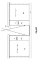
- FIG. 3 shows a cross-sectional view of a preferred super junction trench MOSFET (STM) according to the present invention, wherein a super junction structure which is similar to FIG. 2 is integrated with an N-channel trench MOSFET 300 .
- the super junction structure comprising a second N epitaxial layer 304 in a deep trench 303 is formed in a first N epitaxial layer 302 which comprises a first type N column regions 305 and a second type P column regions 306 .
- P body regions 310 are extending onto the super junction structure and are spaced apart from each other by a plurality of trenched gates 312 which are extending into the first type N column regions 305 and the second N epitaxial layer 304 .
- At least one trenched source-body contact structure 314 is penetrating through a contact interlayer 316 and extending into the P body regions 310 .
- a plurality of n+ source regions 318 are formed surrounding the trenched gates 312 and only located between sidewalls of the trenched gates 312 and the adjacent trenched source-body contact structure 314 . Therefore, the n+ source regions 308 and the P body regions 310 are connected to a source metal 320 via the trenched source-body contact structure 314 which is filled with a contact metal plug (not shown).
- a p+ ohmic body doped region 322 is formed surrounding at least bottom of each the trenched source-body contact structure 314 to reduce the contact resistance between the P body regions 310 and the contact metal plug filled in the trenched source-body contact structure 314 .
- a drain metal 322 is formed on a bottom surface of the N+ substrate layer 301 .
- the trenched gates 312 can be implemented by a doped poly-silicon layer padded by a gate oxide layer 311 ;
- the contact interlayer 316 can be implemented by a BPSG (Boron Phosphorus Silicon Glass) layer 316 - 1 and a NSG (non-doped Silicon Glass) layer 316 - 2 ;
- the contact metal plug formed in the trenched source-body contact structure 314 can be implemented by using a tungsten plug padded by a barrier layer of Ti/TiN or Co/TiN or Ta/TiN;
- the source metal 320 can be padded by a resistance-reduction layer (not shown) to reduce the contact resistance between the source metal 320 and the contact metal plug formed in the trenched source-body contact structure 314 .
- FIG. 4 shows a cross-sectional view of another preferred N-channel trench MOSFET 400 integrated with a super junction structure according to the present invention, compared to FIG. 3 , FIG. 4 further comprises a termination structure including multiple guard rings 410 formed near top surface of the first N epitaxial layer 402 , wherein one of the guard rings 411 nearest to the P body region 410 is contacting with the P body region 410 and is connected to the source metal 420 via a trenched body contact structure 415 .
- the source metal 420 further extends to cover a portion of the guard rings to function as a field plate.
- FIG. 5 shows a cross-sectional view of another preferred N-channel trench MOSFET 500 integrated with a super junction structure according to the present invention, compared to FIG. 3 , FIG. 5 further comprises a charge balance termination structure including an EPR 522 onto the contact interlayer 516 , and an n+ channel stop region 524 near top surface of the first N epitaxial layer 502 .
- first N epitaxial layer 502 is shorted to the EPR metal 522 via a trenched EPR contact 526 which has sidewalls surrounded by the n+ channel stop region 524 in the first N epitaxial layer 502 and has a bottom surrounded by a p+ doped region 528 which are formed at the same step with the p+ ohmic body doped regions 530 .
- FIGS. 6A to 6J are a serial of exemplary steps that are performed to form the preferred embodiment as shown in FIG. 3 .
- a first N epitaxial layer 302 is grown on an N+ substrate layer 301 , wherein the N+ substrate layer 301 has a greater doping concentration than the first N epitaxial layer 302 , and shares a common interface 301 ′ with the first N epitaxial layer 302 .
- a deep trench mask 305 is applied covering top surface of the first N epitaxial layer 302 , and a deep trench 303 is etched through the deep trench mask 305 , the first N epitaxial layer 302 and extending into the N+ substrate layer 301 by successively dry oxide etch and dry silicon etch. Therefore, the deep trench 303 has a bottom lower than the common interface 301 ′.
- an isotropic dry etch about 500 ⁇ per side is carried out in down stream plasma to remove the silicon damage during opening the deep trench 303 .
- a pad oxide 307 about 100 ⁇ is first grown lining inner surface of the deep trench 303 .
- angle ion implantations with Phosphorus dopant are carried out through sidewalls of the deep trench 303 , and followed by a Phosphorus dopant drive-in for formation of a first type N column regions 305 .
- FIG. 6D another angle ion implantations with Boron dopant are carried out through sidewalls of the deep trench 303 , and followed by a diffusion step for formation of a second type P column regions 306 , which is adjacent to the first type N column regions 305 and surrounding sidewalls of the deep trench 303 .
- the deep trench mask is first removed, and a second N epitaxial layer 304 is formed and is then etched by CMP to leave necessary portion filling into the deep trench 303 .
- a body mask 305 ′ is first applied covering top surface of the super junction structure in FIG. 6E , then an ion implantation with P body dopant is carried out and followed by a diffusion step to form P body regions 310 .
- a gate mask (not shown) is applied for etching a plurality of gate trenches 313 which are some extending into the first type N column regions 306 and some extending into the second N epitaxial layer 304 . Then a sacrificial oxide layer is grown and then removed to eliminate the silicon damage during opening those gate trenches 313 . Next, a gate oxide layer 311 is formed along inner surface of the gate trenches 313 and onto top surface of the P body regions 310 . Then, a doped poly-silicon layer is deposited onto the gate oxide layer 311 and is then etched to leave necessary portion in the gate trenches 313 to form a plurality of trenched gates 312 .
- a source mask 315 is first applied for a source ion implantation with source dopant, then a source dopant diffusion step is carried out for formation of a plurality of n+ source regions near top surface of the P body regions 310 and surrounding the trenched gates 312 .
- a BPSG layer 316 - 1 and an NSG layer 316 - 2 are successively deposited to act as a contact interlayer 316 .
- a contact mask (not shown) is applied for etching a plurality of contact openings 319 by successively dry oxide etch and dry silicon etch, wherein the contact openings 319 are penetrating through the contact interlayer 316 and extending into the P body regions 310 .
- the n+ source regions 318 are only located between the contact openings 319 and the adjacent trenched gates 312 , not between two adjacent contact openings 319 .
- a BF2 ion implantation is performed to form a p+ ohmic body doped region in the P body regions 310 and surrounding at least bottom of each of the contact openings 319 .
- a step of RTA Rapid Thermal Annealing
- a layer of Ti/TiN or Co/TiN or Ta/TiN (not shown) and material tungsten are successively deposited and then etched back to leave necessary portion in the contact openings 319 (as shown in FIG. 6I ) to act as a contact metal plug 314 ′ for a trenched source-body contact structure 314 .
- metal Al alloys padded by a Ti or Ti/TiN layer is deposited and is then patterned after applying a metal mask (not shown) by metal etch to form a source metal 320 .
- a drain metal 322 is deposited on a bottom surface of the N+ substrate layer 301 after backside grinding.
Landscapes
- Engineering & Computer Science (AREA)
- Microelectronics & Electronic Packaging (AREA)
- Power Engineering (AREA)
- Physics & Mathematics (AREA)
- Condensed Matter Physics & Semiconductors (AREA)
- General Physics & Mathematics (AREA)
- Computer Hardware Design (AREA)
- Manufacturing & Machinery (AREA)
- Ceramic Engineering (AREA)
- Chemical & Material Sciences (AREA)
- Plasma & Fusion (AREA)
- Composite Materials (AREA)
- Chemical Kinetics & Catalysis (AREA)
- General Chemical & Material Sciences (AREA)
- High Energy & Nuclear Physics (AREA)
- Electrodes Of Semiconductors (AREA)
- Crystallography & Structural Chemistry (AREA)
- Health & Medical Sciences (AREA)
- Toxicology (AREA)
- Metal-Oxide And Bipolar Metal-Oxide Semiconductor Integrated Circuits (AREA)
Abstract
A method for manufacturing a super junction trench MOSFET by growing a first epitaxial layer of a first conductivity type upon a heavily doped substrate layer of a first conductivity type; forming a deep trench mask covering a top surface of the first epitaxial layer; applying a trench mask to form a deep trench extending into the substrate layer by successively dry oxide etch and dry silicon etch; and carrying out angle ion implantations of the first conductivity type dopant and driving-in to form a first type column regions with column shape within the first epitaxial layer; and carrying out angle ion implantations of a second conductivity type dopant and diffusion to form a second type column regions with column shape adjacent to sidewalls of the deep trench, in parallel with and surrounding the first type column regions; and removing the hard mask.
Description
This invention relates generally to the cell structure, device configuration and fabrication process of power semiconductor devices. More particularly, this invention relates to a novel and improved cell structure, device configuration and improved process of super-junction structures.
Super-junction structures are more and more attractive due to higher breakdown voltage and lower specific Rds (drain-source resistance). As is known to all, a super-junction structure is implemented by p type column structures and n type column structures arranged in parallel and connecting to each other onto a heavily doped substrate, however, the manufacturing yield is not stable because the super-junction structure is very sensitive to the fabrication processes and conditions such as: the p type column structures and n type column structures dopant re-diffusion issue induced by subsequent thermal processes; trapped charges within the column structures, etc. . . . . All that will cause a hazardous condition of charges imbalance to the super-junction structure. More specifically, these undesired influences become more pronounced with a narrower column structure width for a lower bias voltage ranging under 200V.
U.S. Pat. No. 7,601,597 disclosed a method to avoid the aforementioned p type column structure and n type structure dopant re-diffusion issue, for example, in an N-channel super-junction trench MOSFET (Metal Oxide Semiconductor Field Effect Transistor, the same herein after) as shown in FIG. 1 , by setting up the p type column formation process in a deep trench at a last step after all diffusion processes such as: sacrificial oxidation after trench etch, gate oxidation, P body region formation and n+ source region formation, etc have been finished.
However, in order to achieve a shorter growth time of the p type epitaxial layer without having void formation in the deep trenches, a greater CD (Critical Dimension) is required, e.g., trench width of the deep trench must be greater than 4.0 um if the deep trench having 40 um depth. On the other hand, the deep trench filled with p type epitaxial layer and having a greater trench width will occupy a large amount of active areas, causing high specific Rds.
Moreover, other factors such as: the charges imbalance caused by the trapped charges within the column structure is still not resolved.
Therefore, there is still a need in the art of the semiconductor power device, particularly for super-junction design and fabrication, to provide a novel cell structure, device configuration that would resolve these difficulties and design limitations.
The present invention provides a super junction structure having implanted regions surrounding an N epitaxial layer in a deep trench to resolve the problems discussed above, wherein the implanted regions are P and N type column regions, which are formed by angle implantation through sidewalls of the deep trench into an N epitaxial layer on an N+ substrate. Therefore, the deep trench filled with the N type epitaxial layer surrounded with the P and N type column regions forms a charge balance area for sustaining high breakdown voltage. Furthermore, since the deep trench filled with the N type epitaxial layer, the specific Rds is significantly reduced because channel regions are capable of forming in the N type epitaxial layer in the deep trench. The inventive super junction structure can be used for power semiconductor power devices, such as: MOSFET and Schottky rectifier.
According to one aspect, the present invention features a super junction structure comprising: a first epitaxial layer of a first conductivity type formed on a substrate layer of the same conductivity type, wherein the first epitaxial layer has a lower doping concentration than the substrate layer; a deep trench penetrating through the first epitaxial layer and extending into the substrate layer; a second epitaxial layer of the first conductivity type formed in the deep trench; a first type column regions of the first conductivity type formed in the first epitaxial layer; a second type column regions of a second conductivity type formed in the first epitaxial layer and close to the first type column regions, surrounding the deep trench and arranged in parallel with the first type column regions and the deep trench.
According to another aspect, the present invention features a super junction structure integrated with a trench MOSFET structure, further comprising: a body region of the second conductivity type extending over the super junction structure; a plurality of trenched gates penetrating through the body region and extending into the first type column regions and the second epitaxial layer; at least one trenched source-body contact structure located between every two adjacent of the trenched gates; a source region of the first conductivity type extending between the trenched source-body contact structure and the adjacent trenched gate.
According to another aspect of the present invention, the inventive super junction structure integrated with the trench MOSFET structure further comprises a termination structure surrounding outer of the super junction structure and the trench MOSFET structure, wherein the termination structure further comprises multiple guard rings formed near surface of the first epitaxial layer to sustain a high breakdown voltage.
According to another aspect of the present invention, the inventive super junction structure integrated with the trench MOSFET structure further comprises a charge balance termination structure surrounding outer of the super junction structure and the trench MOSFET structure, wherein the charge balance termination structure further comprises a trenched EPR (equal potential ring) contact structure connecting the first epitaxial layer to an EPR metal layer, wherein the trenched EPR contact structure has sidewalls surrounded by a channel stop region of the first conductivity type in the first epitaxial layer.
The invention also features a method of making a super junction trench MOSFET including: (a) growing a first epitaxial layer of a first conductivity type upon a heavily doped substrate layer of the first conductivity type; (b) forming a deep trench mask covering a top surface of the first epitaxial layer; (c) applying a trench mask to form a deep trench extending into the substrate layer by successively dry oxide etch and dry silicon etch; (d) carrying out angle ion implantations of the first conductivity type dopant and driving-in to form a first type column regions with column shape within the first epitaxial layer; (e) carrying out angle ion implantations of a second conductivity type dopant and diffusion to form a second type column regions with column shape adjacent to sidewalls of the deep trench, in parallel with and surrounding the first type column regions; and (f) removing said hard mask.
These and other objects and advantages of the present invention will no doubt become obvious to those of ordinary skill in the art after having read the following detailed description of the preferred embodiment, which is illustrated in the various drawing figures.
The present invention can be more fully understood by reading the following detailed description of the preferred embodiments, with reference made to the accompanying drawings, wherein:
In the following Detailed Description, reference is made to the accompanying drawings, which forms a part thereof, and in which is shown by way of illustration specific embodiments in which the invention may be practiced. In this regard, directional terminology, such as “top”, “bottom”, “front”, “back”, etc., is used with reference to the orientation of the Figure(s) being described. Because components of embodiments can be positioned in a number of different orientations, the directional terminology is used for purpose of illustration and is in no way limiting. It is to be understood that other embodiments may be utilized and structural or logical changes may be make without departing from the scope of the present invention. The following detailed description, therefore, is not to be taken in a limiting sense, and the scope of the present invention is defined by the appended claims. It is to be understood that the features of the various exemplary embodiments described herein may be combined with each other, unless specifically noted otherwise.
Please refer to FIG. 2 for a preferred embodiment of this invention, wherein a super junction structure 200 formed in a first N epitaxial layer 202 onto an N+ substrate layer 201 is disclosed. According to the present invention, the super junction structure 200 comprises a deep trench 203 penetrating through the first N epitaxial layer 202 and extending into the N+ substrate layer 201, which means the deep trench 203 has a bottom lower than interface between the first N epitaxial layer 202 and the N+ substrate 201. Into the deep trench 203, a second N epitaxial layer 204 is formed refilling the deep trench. A first type N column regions 205 and a second type P column regions 206 are formed in parallel in the first N epitaxial layer 201, wherein, the second type P column regions 206 surrounding the deep trench 203 are located between the first type N column regions 205 and the deep trench 203. The inventive super junction structure can be used for semiconductor power devices such as: MOSFET and Schottky diode.
In FIG. 6B , an isotropic dry etch about 500 Å per side is carried out in down stream plasma to remove the silicon damage during opening the deep trench 303.
In FIG. 6C , a pad oxide 307 about 100 Å is first grown lining inner surface of the deep trench 303. Next, angle ion implantations with Phosphorus dopant are carried out through sidewalls of the deep trench 303, and followed by a Phosphorus dopant drive-in for formation of a first type N column regions 305.
In FIG. 6D , another angle ion implantations with Boron dopant are carried out through sidewalls of the deep trench 303, and followed by a diffusion step for formation of a second type P column regions 306, which is adjacent to the first type N column regions 305 and surrounding sidewalls of the deep trench 303.
In FIG. 6E , the deep trench mask is first removed, and a second N epitaxial layer 304 is formed and is then etched by CMP to leave necessary portion filling into the deep trench 303.
In FIG. 6F , a body mask 305′ is first applied covering top surface of the super junction structure in FIG. 6E , then an ion implantation with P body dopant is carried out and followed by a diffusion step to form P body regions 310.
In FIG. 6G , after the body mask 305′ is removed, a gate mask (not shown) is applied for etching a plurality of gate trenches 313 which are some extending into the first type N column regions 306 and some extending into the second N epitaxial layer 304. Then a sacrificial oxide layer is grown and then removed to eliminate the silicon damage during opening those gate trenches 313. Next, a gate oxide layer 311 is formed along inner surface of the gate trenches 313 and onto top surface of the P body regions 310. Then, a doped poly-silicon layer is deposited onto the gate oxide layer 311 and is then etched to leave necessary portion in the gate trenches 313 to form a plurality of trenched gates 312.
In FIG. 6H , a source mask 315 is first applied for a source ion implantation with source dopant, then a source dopant diffusion step is carried out for formation of a plurality of n+ source regions near top surface of the P body regions 310 and surrounding the trenched gates 312.
In FIG. 6I , after the source mask 315 is removed, a BPSG layer 316-1 and an NSG layer 316-2 are successively deposited to act as a contact interlayer 316. Then, a contact mask (not shown) is applied for etching a plurality of contact openings 319 by successively dry oxide etch and dry silicon etch, wherein the contact openings 319 are penetrating through the contact interlayer 316 and extending into the P body regions 310. What should be noticed is that, the n+ source regions 318 are only located between the contact openings 319 and the adjacent trenched gates 312, not between two adjacent contact openings 319. Next, a BF2 ion implantation is performed to form a p+ ohmic body doped region in the P body regions 310 and surrounding at least bottom of each of the contact openings 319. After that, a step of RTA (Rapid Thermal Annealing) is performed.
In FIG. 6J , a layer of Ti/TiN or Co/TiN or Ta/TiN (not shown) and material tungsten are successively deposited and then etched back to leave necessary portion in the contact openings 319 (as shown in FIG. 6I ) to act as a contact metal plug 314′ for a trenched source-body contact structure 314. Then, metal Al alloys padded by a Ti or Ti/TiN layer (not shown) is deposited and is then patterned after applying a metal mask (not shown) by metal etch to form a source metal 320. Next, a drain metal 322 is deposited on a bottom surface of the N+ substrate layer 301 after backside grinding.
Although the present invention has been described in terms of the presently preferred embodiments, it is to be understood that such disclosure is not to be interpreted as limiting. Various alternations and modifications will no doubt become apparent to those skilled in the art after reading the above disclosure. Accordingly, it is intended that the appended claims be interpreted as covering all alternations and modifications as fall within the true spirit and scope of the invention.
Claims (3)
1. A method for manufacturing a super junction trench MOSFET comprising the steps of:
growing a first epitaxial layer structure of a first conductivity type upon a heavily doped substrate layer of said first conductivity type;
forming a deep trench mask covering a top surface of said first epitaxial layer;
applying a trench mask to form a deep trench structure extending into said substrate layer by successively dry oxide etch and dry silicon etch;
carrying out angle ion implantations of said first conductivity type dopant and driving-in to form a first type column structures with column shape within said first epitaxial layer;
carrying out angle ion implantations of a second conductivity type dopant and diffusion to form a second type column structures with column shape adjacent to sidewalls of said deep trench structure, in parallel with and surrounding said first type column structures; removing said deep trench mask;
forming a second epitaxial layer of said first conductivity type into said deep trench structure;
applying a body mask and carrying out body ion implantation over the above said structures to form body regions;
applying a gate mask to etch a plurality of gate trenches through said body regions and extending into said first type column structures and said second epitaxial layer;
growing a sacrificial oxide layer onto inner surface of said gate trenches and remove to eliminate the plasma damage;
growing a gate oxide layer along an inner surface of said gate trenches;
depositing a doped poly-silicon layer to fill said gate trenches;
etching back said doped poly-silicon layer by CMP or plasma etch to serve as a plurality of trenched gates;
applying a source mask and carrying out source ion implantation;
depositing a contact interlayer; and
applying a contact mask and etching a plurality of contact openings through said contact interlayer and extending into said body regions, wherein source regions are located only between each of said contact openings and an adjacent trenched gate.
2. The method of claim 1 , after etching said deep trench, further comprising isotropic dry etch about 500 Å in downstream plasma to remove silicon damage during etching said deep trench.
3. The method of claim 1 , before carrying out angle ion implantation of said first conductivity type dopant, further comprising growing a pad oxide about 100 Å along inner surface of said deep trench.
Priority Applications (1)
| Application Number | Priority Date | Filing Date | Title |
|---|---|---|---|
| US14/799,878 US9530867B2 (en) | 2013-09-19 | 2015-07-15 | Method for manufacturing a super-junction structures having implanted regions surrounding an N epitaxial layer in deep trench |
Applications Claiming Priority (2)
| Application Number | Priority Date | Filing Date | Title |
|---|---|---|---|
| US14/031,089 US9099320B2 (en) | 2013-09-19 | 2013-09-19 | Super-junction structures having implanted regions surrounding an N epitaxial layer in deep trench |
| US14/799,878 US9530867B2 (en) | 2013-09-19 | 2015-07-15 | Method for manufacturing a super-junction structures having implanted regions surrounding an N epitaxial layer in deep trench |
Related Parent Applications (1)
| Application Number | Title | Priority Date | Filing Date |
|---|---|---|---|
| US14/031,089 Division US9099320B2 (en) | 2013-09-19 | 2013-09-19 | Super-junction structures having implanted regions surrounding an N epitaxial layer in deep trench |
Publications (2)
| Publication Number | Publication Date |
|---|---|
| US20150318379A1 US20150318379A1 (en) | 2015-11-05 |
| US9530867B2 true US9530867B2 (en) | 2016-12-27 |
Family
ID=52667204
Family Applications (2)
| Application Number | Title | Priority Date | Filing Date |
|---|---|---|---|
| US14/031,089 Active 2033-12-04 US9099320B2 (en) | 2013-09-19 | 2013-09-19 | Super-junction structures having implanted regions surrounding an N epitaxial layer in deep trench |
| US14/799,878 Active US9530867B2 (en) | 2013-09-19 | 2015-07-15 | Method for manufacturing a super-junction structures having implanted regions surrounding an N epitaxial layer in deep trench |
Family Applications Before (1)
| Application Number | Title | Priority Date | Filing Date |
|---|---|---|---|
| US14/031,089 Active 2033-12-04 US9099320B2 (en) | 2013-09-19 | 2013-09-19 | Super-junction structures having implanted regions surrounding an N epitaxial layer in deep trench |
Country Status (1)
| Country | Link |
|---|---|
| US (2) | US9099320B2 (en) |
Cited By (1)
| Publication number | Priority date | Publication date | Assignee | Title |
|---|---|---|---|---|
| US20220020858A1 (en) * | 2020-07-16 | 2022-01-20 | Shanghai Huahong Grace Semiconductor Manufacturing Corporation | Trench gate device and method for making the same |
Families Citing this family (28)
| Publication number | Priority date | Publication date | Assignee | Title |
|---|---|---|---|---|
| US9653598B2 (en) * | 2013-11-15 | 2017-05-16 | Infineon Technologies Austria Ag | Transistor component |
| JP6237408B2 (en) * | 2014-03-28 | 2017-11-29 | 住友電気工業株式会社 | Silicon carbide semiconductor device and manufacturing method thereof |
| DE102014112371B4 (en) * | 2014-08-28 | 2023-11-23 | Infineon Technologies Austria Ag | SEMICONDUCTOR DEVICE AND ELECTRONIC ARRANGEMENT COMPRISING A SEMICONDUCTOR DEVICE |
| JP6514519B2 (en) | 2015-02-16 | 2019-05-15 | ルネサスエレクトロニクス株式会社 | Semiconductor device manufacturing method |
| WO2017130374A1 (en) * | 2016-01-29 | 2017-08-03 | 新電元工業株式会社 | Power semiconductor device and method for manufacturing power semiconductor device |
| DE102016226237A1 (en) | 2016-02-01 | 2017-08-03 | Fuji Electric Co., Ltd. | SILICON CARBIDE SEMICONDUCTOR DEVICE AND METHOD FOR PRODUCING A SILICON CARBIDE SEMICONDUCTOR DEVICE |
| JP6472776B2 (en) | 2016-02-01 | 2019-02-20 | 富士電機株式会社 | Silicon carbide semiconductor device and method for manufacturing silicon carbide semiconductor device |
| WO2017168736A1 (en) * | 2016-03-31 | 2017-10-05 | 新電元工業株式会社 | Semiconductor device and production method for semiconductor device |
| CN109148556B (en) * | 2017-06-27 | 2022-02-15 | 深圳尚阳通科技有限公司 | Super junction device and manufacturing method thereof |
| CN109148555B (en) * | 2017-06-27 | 2021-08-31 | 深圳尚阳通科技有限公司 | Super junction device and manufacturing method thereof |
| CN109148558B (en) * | 2017-06-27 | 2021-08-10 | 深圳尚阳通科技有限公司 | Super junction device and manufacturing method thereof |
| CN109148557B (en) * | 2017-06-27 | 2021-06-11 | 深圳尚阳通科技有限公司 | Super junction device and manufacturing method thereof |
| US11056585B2 (en) | 2018-04-20 | 2021-07-06 | Ipower Semiconductor | Small pitch super junction MOSFET structure and method |
| US11069770B2 (en) * | 2018-10-01 | 2021-07-20 | Ipower Semiconductor | Carrier injection control fast recovery diode structures |
| CN111200008B (en) * | 2018-11-20 | 2023-08-22 | 深圳尚阳通科技股份有限公司 | Superjunction device and method of manufacturing the same |
| US11127852B2 (en) * | 2018-12-27 | 2021-09-21 | Texas Instruments Incorporated | Vertical trench gate MOSFET with deep well region for junction termination |
| US11031472B2 (en) | 2018-12-28 | 2021-06-08 | General Electric Company | Systems and methods for integrated diode field-effect transistor semiconductor devices |
| CN110010693B (en) * | 2019-05-07 | 2024-03-12 | 无锡紫光微电子有限公司 | Structure of high-voltage deep trench type super-junction MOSFET and manufacturing method thereof |
| US11205720B2 (en) * | 2019-05-30 | 2021-12-21 | Rohm Co., Ltd. | Semiconductor device with contact plugs |
| DE102019210285B4 (en) | 2019-07-11 | 2023-09-28 | Infineon Technologies Ag | Creating a buried cavity in a semiconductor substrate |
| CN110429140A (en) * | 2019-08-06 | 2019-11-08 | 上海朕芯微电子科技有限公司 | A kind of super node MOSFET structure and preparation method thereof |
| CN113628968B (en) * | 2020-05-06 | 2022-06-24 | 苏州东微半导体股份有限公司 | Manufacturing method of semiconductor super junction device |
| CN112002643B (en) * | 2020-08-21 | 2023-08-22 | 上海华虹宏力半导体制造有限公司 | Method for manufacturing super junction device |
| CN111900090B (en) * | 2020-08-26 | 2024-01-23 | 上海华虹宏力半导体制造有限公司 | Method for manufacturing super junction device |
| CN112510079A (en) * | 2020-11-27 | 2021-03-16 | 龙腾半导体股份有限公司 | Charge balance groove super-barrier rectifier and manufacturing method thereof |
| CN113990757B (en) * | 2021-10-27 | 2024-03-26 | 电子科技大学 | MOS device structure and manufacturing method |
| CN116825829A (en) * | 2022-03-21 | 2023-09-29 | 苏州东微半导体股份有限公司 | Semiconductor super junction power device |
| CN115377220A (en) * | 2022-09-14 | 2022-11-22 | 江苏美微科半导体有限公司 | Stepped gradient epitaxial deep trench super junction and preparation method thereof |
Citations (4)
| Publication number | Priority date | Publication date | Assignee | Title |
|---|---|---|---|---|
| US8067800B2 (en) * | 2009-12-28 | 2011-11-29 | Force Mos Technology Co., Ltd. | Super-junction trench MOSFET with resurf step oxide and the method to make the same |
| US20120061754A1 (en) * | 2009-12-28 | 2012-03-15 | Force Mos Technology Co. Ltd. | Super-junction trench mosfet with resurf stepped oxides and split gate electrodes |
| US20140213023A1 (en) * | 2013-01-25 | 2014-07-31 | Anpec Electronics Corporation | Method for fabricating power semiconductor device |
| US20140346593A1 (en) * | 2013-05-22 | 2014-11-27 | Force Mos Technology Co., Ltd. | Super-junction trench mosfets with short terminations |
-
2013
- 2013-09-19 US US14/031,089 patent/US9099320B2/en active Active
-
2015
- 2015-07-15 US US14/799,878 patent/US9530867B2/en active Active
Patent Citations (4)
| Publication number | Priority date | Publication date | Assignee | Title |
|---|---|---|---|---|
| US8067800B2 (en) * | 2009-12-28 | 2011-11-29 | Force Mos Technology Co., Ltd. | Super-junction trench MOSFET with resurf step oxide and the method to make the same |
| US20120061754A1 (en) * | 2009-12-28 | 2012-03-15 | Force Mos Technology Co. Ltd. | Super-junction trench mosfet with resurf stepped oxides and split gate electrodes |
| US20140213023A1 (en) * | 2013-01-25 | 2014-07-31 | Anpec Electronics Corporation | Method for fabricating power semiconductor device |
| US20140346593A1 (en) * | 2013-05-22 | 2014-11-27 | Force Mos Technology Co., Ltd. | Super-junction trench mosfets with short terminations |
Cited By (2)
| Publication number | Priority date | Publication date | Assignee | Title |
|---|---|---|---|---|
| US20220020858A1 (en) * | 2020-07-16 | 2022-01-20 | Shanghai Huahong Grace Semiconductor Manufacturing Corporation | Trench gate device and method for making the same |
| US11527633B2 (en) * | 2020-07-16 | 2022-12-13 | Shanghai Huahong Grace Semiconductor Manufacturing Corporation | Trench gate device and method for making the same |
Also Published As
| Publication number | Publication date |
|---|---|
| US20150318379A1 (en) | 2015-11-05 |
| US9099320B2 (en) | 2015-08-04 |
| US20150076594A1 (en) | 2015-03-19 |
Similar Documents
| Publication | Publication Date | Title |
|---|---|---|
| US9530867B2 (en) | Method for manufacturing a super-junction structures having implanted regions surrounding an N epitaxial layer in deep trench | |
| US8564058B1 (en) | Super-junction trench MOSFET with multiple trenched gates in unit cell | |
| US8373224B2 (en) | Super-junction trench MOSFET with resurf stepped oxides and trenched contacts | |
| US8587054B2 (en) | Trench MOSFET with resurf stepped oxide and diffused drift region | |
| US8372717B2 (en) | Method for manufacturing a super-junction trench MOSFET with resurf stepped oxides and trenched contacts | |
| US8373225B2 (en) | Super-junction trench MOSFET with Resurf stepped oxides and split gate electrodes | |
| US8067800B2 (en) | Super-junction trench MOSFET with resurf step oxide and the method to make the same | |
| US8829607B1 (en) | Fast switching super-junction trench MOSFETs | |
| US8525255B2 (en) | Trench MOSFET with trenched floating gates having thick trench bottom oxide as termination | |
| US20210028305A1 (en) | Trench mosfets with oxide charge balance region in active area and junction charge balance region in termination area | |
| US8022471B2 (en) | Trench metal oxide semiconductor field effect transistor (MOSFET) with low gate to drain coupled charges (Qgd) structures | |
| US20120080748A1 (en) | Trench mosfet with super pinch-off regions | |
| US8652900B2 (en) | Trench MOSFET with ultra high cell density and manufacture thereof | |
| US8999789B2 (en) | Super-junction trench MOSFETs with short terminations | |
| US20210384346A1 (en) | Shielded gate trench mosfet having super junction surrounding lower portion of trenched gates | |
| US20090085107A1 (en) | Trench MOSFET with thick bottom oxide tub | |
| US20130214350A1 (en) | Integrated trench mosfet with trench schottky rectifier | |
| US9530882B1 (en) | Trench MOSFET with shielded gate and diffused drift region | |
| US20130256786A1 (en) | Trench mosfet with shielded electrode and avalanche enhancement region | |
| US9018701B2 (en) | Avalanche capability improvement in power semiconductor devices using three masks process | |
| US8564054B2 (en) | Trench semiconductor power device having active cells under gate metal pad | |
| JP2016021547A (en) | Semiconductor device manufacturing method | |
| US8933507B2 (en) | Metal/polysilicon gate trench power mosfet | |
| US9293527B1 (en) | Super-junction trench MOSFET structure | |
| US20090206395A1 (en) | Trench mosfet with double epitaxial structure |
Legal Events
| Date | Code | Title | Description |
|---|---|---|---|
| AS | Assignment |
Owner name: FORCE MOS TECHNOLOGY CO, LTD., TAIWAN Free format text: ASSIGNMENT OF ASSIGNORS INTEREST;ASSIGNOR:HSIEH, FU-YUAN;REEL/FRAME:036095/0280 Effective date: 20130911 |
|
| STCF | Information on status: patent grant |
Free format text: PATENTED CASE |
|
| MAFP | Maintenance fee payment |
Free format text: PAYMENT OF MAINTENANCE FEE, 4TH YR, SMALL ENTITY (ORIGINAL EVENT CODE: M2551); ENTITY STATUS OF PATENT OWNER: SMALL ENTITY Year of fee payment: 4 |