US9530833B2 - Semiconductor structure including capacitors having different capacitor dielectrics and method for the formation thereof - Google Patents
Semiconductor structure including capacitors having different capacitor dielectrics and method for the formation thereof Download PDFInfo
- Publication number
- US9530833B2 US9530833B2 US14/307,078 US201414307078A US9530833B2 US 9530833 B2 US9530833 B2 US 9530833B2 US 201414307078 A US201414307078 A US 201414307078A US 9530833 B2 US9530833 B2 US 9530833B2
- Authority
- US
- United States
- Prior art keywords
- capacitor
- layer
- electrode
- dielectric
- electrically conductive
- Prior art date
- Legal status (The legal status is an assumption and is not a legal conclusion. Google has not performed a legal analysis and makes no representation as to the accuracy of the status listed.)
- Active, expires
Links
Images


Classifications
-
- H01L28/55—
-
- H—ELECTRICITY
- H10—SEMICONDUCTOR DEVICES; ELECTRIC SOLID-STATE DEVICES NOT OTHERWISE PROVIDED FOR
- H10D—INORGANIC ELECTRIC SEMICONDUCTOR DEVICES
- H10D1/00—Resistors, capacitors or inductors
- H10D1/60—Capacitors
- H10D1/68—Capacitors having no potential barriers
- H10D1/682—Capacitors having no potential barriers having dielectrics comprising perovskite structures
-
- H01L27/0805—
-
- H01L27/11502—
-
- H01L28/40—
-
- H—ELECTRICITY
- H10—SEMICONDUCTOR DEVICES; ELECTRIC SOLID-STATE DEVICES NOT OTHERWISE PROVIDED FOR
- H10B—ELECTRONIC MEMORY DEVICES
- H10B53/00—Ferroelectric RAM [FeRAM] devices comprising ferroelectric memory capacitors
-
- H—ELECTRICITY
- H10—SEMICONDUCTOR DEVICES; ELECTRIC SOLID-STATE DEVICES NOT OTHERWISE PROVIDED FOR
- H10D—INORGANIC ELECTRIC SEMICONDUCTOR DEVICES
- H10D1/00—Resistors, capacitors or inductors
- H10D1/60—Capacitors
- H10D1/68—Capacitors having no potential barriers
-
- H—ELECTRICITY
- H10—SEMICONDUCTOR DEVICES; ELECTRIC SOLID-STATE DEVICES NOT OTHERWISE PROVIDED FOR
- H10D—INORGANIC ELECTRIC SEMICONDUCTOR DEVICES
- H10D84/00—Integrated devices formed in or on semiconductor substrates that comprise only semiconducting layers, e.g. on Si wafers or on GaAs-on-Si wafers
- H10D84/201—Integrated devices formed in or on semiconductor substrates that comprise only semiconducting layers, e.g. on Si wafers or on GaAs-on-Si wafers characterised by the integration of only components covered by H10D1/00 or H10D8/00, e.g. RLC circuits
- H10D84/204—Integrated devices formed in or on semiconductor substrates that comprise only semiconducting layers, e.g. on Si wafers or on GaAs-on-Si wafers characterised by the integration of only components covered by H10D1/00 or H10D8/00, e.g. RLC circuits of combinations of diodes or capacitors or resistors
- H10D84/212—Integrated devices formed in or on semiconductor substrates that comprise only semiconducting layers, e.g. on Si wafers or on GaAs-on-Si wafers characterised by the integration of only components covered by H10D1/00 or H10D8/00, e.g. RLC circuits of combinations of diodes or capacitors or resistors of only capacitors
-
- H—ELECTRICITY
- H10—SEMICONDUCTOR DEVICES; ELECTRIC SOLID-STATE DEVICES NOT OTHERWISE PROVIDED FOR
- H10W—GENERIC PACKAGES, INTERCONNECTIONS, CONNECTORS OR OTHER CONSTRUCTIONAL DETAILS OF DEVICES COVERED BY CLASS H10
- H10W20/00—Interconnections in chips, wafers or substrates
- H10W20/01—Manufacture or treatment
- H10W20/071—Manufacture or treatment of dielectric parts thereof
- H10W20/081—Manufacture or treatment of dielectric parts thereof by forming openings in the dielectric parts
- H10W20/083—Manufacture or treatment of dielectric parts thereof by forming openings in the dielectric parts the openings being via holes penetrating underlying conductors
-
- H—ELECTRICITY
- H10—SEMICONDUCTOR DEVICES; ELECTRIC SOLID-STATE DEVICES NOT OTHERWISE PROVIDED FOR
- H10W—GENERIC PACKAGES, INTERCONNECTIONS, CONNECTORS OR OTHER CONSTRUCTIONAL DETAILS OF DEVICES COVERED BY CLASS H10
- H10W20/00—Interconnections in chips, wafers or substrates
- H10W20/40—Interconnections external to wafers or substrates, e.g. back-end-of-line [BEOL] metallisations or vias connecting to gate electrodes
- H10W20/41—Interconnections external to wafers or substrates, e.g. back-end-of-line [BEOL] metallisations or vias connecting to gate electrodes characterised by their conductive parts
- H10W20/42—Vias, e.g. via plugs
-
- H—ELECTRICITY
- H10—SEMICONDUCTOR DEVICES; ELECTRIC SOLID-STATE DEVICES NOT OTHERWISE PROVIDED FOR
- H10W—GENERIC PACKAGES, INTERCONNECTIONS, CONNECTORS OR OTHER CONSTRUCTIONAL DETAILS OF DEVICES COVERED BY CLASS H10
- H10W20/00—Interconnections in chips, wafers or substrates
- H10W20/40—Interconnections external to wafers or substrates, e.g. back-end-of-line [BEOL] metallisations or vias connecting to gate electrodes
- H10W20/495—Capacitive arrangements or effects of, or between wiring layers
- H10W20/496—Capacitor integral with wiring layers
-
- H01L27/1085—
-
- H—ELECTRICITY
- H10—SEMICONDUCTOR DEVICES; ELECTRIC SOLID-STATE DEVICES NOT OTHERWISE PROVIDED FOR
- H10B—ELECTRONIC MEMORY DEVICES
- H10B12/00—Dynamic random access memory [DRAM] devices
- H10B12/01—Manufacture or treatment
- H10B12/02—Manufacture or treatment for one transistor one-capacitor [1T-1C] memory cells
- H10B12/03—Making the capacitor or connections thereto
Definitions
- the present disclosure relates to the field of integrated circuits, and, in particular, to integrated circuits including capacitors having different capacitor dielectrics.
- Integrated circuits typically include a large number of circuit elements, which form an electric circuit.
- integrated circuits may include passive devices such as resistors, inductances and/or capacitors.
- Types of capacitors that may be provided in integrated circuits include metal-insulator-metal capacitors.
- Metal-insulator-metal capacitors may be provided in additional interconnect levels, which are provided in addition to interconnect levels wherein electrically conductive lines connecting circuit elements of integrated circuits are provided.
- Metal-insulator-metal capacitors may be used as decoupling capacitors in CMOS logic integrated circuits to minimize voltage drops at the power grids.
- decoupling capacitors thin films of a high-k dielectric material may be employed as a capacitor dielectric to obtain a high capacitance density of the decoupling capacitors and a low leakage current.
- Other applications of metal-insulator-metal capacitors include filter and analog capacitors, for example, in analog-to-digital converters or digital-to-analog converters, radio frequency coupling capacitors and radio frequency bypass capacitors in radio frequency oscillators, resonator circuits and matching networks.
- nonvolatile embedded memory In many applications of integrated circuits, such as integrated circuits for computers, consumer electronics, communication electronics and automotive electronics, nonvolatile embedded memory is desired.
- Types of nonvolatile memory include floating gate-based flash memory.
- integrating floating gate-based flash memory cells into integrated circuits that also include circuitry of another type, such as, for example, logic circuitry may have issues associated therewith, in particular due to the relatively high process complexity of the formation of floating gate-based flash memory cells.
- more than eight additional photo masks may be required when floating gate-based flash memory cells are provided in an integrated circuit, in addition to photo masks that are used for forming other devices of the integrated circuit.
- relatively high voltages may be required, which may lead to further issues due to the need for high voltage transistors in the integrated circuit.
- nonvolatile memory As an alternative to floating gate-based flash memory, other types of nonvolatile memory have been proposed, which include spin-transfer torque magnetoresistive random access memory (STT-MRAM), phase-change memory (PCM) and resistive random access memory (RRAM).
- STT-MRAM spin-transfer torque magnetoresistive random access memory
- PCM phase-change memory
- RRAM resistive random access memory
- Embodiments of the present disclosure provide semiconductor structures and methods for the formation thereof which may provide an improved integration of nonvolatile memory into integrated circuits.
- An illustrative method disclosed herein includes providing a semiconductor structure.
- the semiconductor structure includes a first interlayer dielectric provided over a semiconductor substrate.
- a first electrode of a first capacitor is formed over the first interlayer dielectric.
- a layer of first dielectric material is deposited over the first electrode of the first capacitor and the first interlayer dielectric.
- a layer of electrically conductive material is deposited over the layer of first dielectric material.
- a second electrode of the first capacitor and a first electrode of the second capacitor are formed from the layer of electrically conductive material. After the formation of the second electrode of the first capacitor and the first electrode of the second capacitor, a layer of second dielectric material is deposited and a second electrode of the second capacitor is formed over the layer of second dielectric material.
- An illustrative semiconductor structure disclosed herein includes an interlayer dielectric provided over a semiconductor substrate, a first capacitor and a second capacitor. Each of the first capacitor and the second capacitor includes a first electrode and a second electrode and is arranged over the interlayer dielectric.
- the semiconductor structure further includes a layer of substantially non-ferroelectric dielectric material and a layer of ferroelectric dielectric material.
- the layer of substantially non-ferroelectric dielectric material includes a first portion and a second portion. The first portion is arranged between the first electrode and the second electrode of the first capacitor and provides a capacitor dielectric of the first capacitor. The second portion is arranged between the interlayer dielectric and the first electrode of the second capacitor.
- the layer of ferroelectric dielectric material includes a first portion arranged between the first electrode and the second electrode of the second capacitor and provides a capacitor dielectric of the second capacitor.
- Another illustrative method disclosed herein includes providing a semiconductor structure comprising a first interlayer dielectric provided over a semiconductor substrate. A first electrode of a capacitor is formed over the interlayer dielectric. A layer of a ferroelectric dielectric material is formed over the first electrode. A second electrode of the capacitor is formed over the ferroelectric dielectric material.
- FIGS. 1-5 show schematic cross-sectional views of a semiconductor structure according to an embodiment in stages of a manufacturing process according to an embodiment
- FIGS. 6-9 show schematic cross-sectional views of a semiconductor structure according to an embodiment in stages of a manufacturing process according to an embodiment
- FIG. 10 shows a circuit diagram of a nonvolatile memory cell in a semiconductor structure according to an embodiment
- FIG. 11 shows an enlarged view of a portion of a schematic cross-sectional view of a semiconductor structure according to an embodiment in a stage of a manufacturing process according to an embodiment.
- the present disclosure provides a process integration scheme that allows a fabrication of both decoupling metal-insulator-metal capacitors and ferroelectric metal-insulator-metal capacitors in a standard CMOS logic process.
- Each of the ferroelectric metal-insulator-metal capacitors may be employed for forming a nonvolatile memory cell, wherein each of the nonvolatile memory cells includes one transistor and one ferroelectric metal-insulator-metal capacitor.
- the ferroelectric metal-insulator-metal capacitor may be a three-dimensional capacitor, which may help to reduce the size of the nonvolatile memory cells. This may be helpful for high density embedded ferroelectric random access memory (FRAM) applications.
- FRAM high density embedded ferroelectric random access memory
- an extra masking and etching may be performed to define a narrow capacitor trench prior to the formation of a metal-insulator-metal stack.
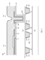
- FIG. 1 shows a schematic cross-sectional view of a semiconductor structure 100 in a stage of a manufacturing process.
- the semiconductor structure 100 includes a substrate 101 .
- the substrate 101 may include a bulk semiconductor substrate, for example, a wafer or die of a semiconductor material, such as silicon.
- the substrate 101 may include a semiconductor-on-insulator substrate that includes a layer of a semiconductor material, such as silicon, provided on a layer of an electrically insulating material, such as silicon dioxide.
- the layer of electrically insulating material may be provided on a support substrate, which may be a silicon wafer or a silicon die.
- the substrate 101 may further include circuit elements of an integrated circuit.
- the substrate 101 may include a plurality of field effect transistors and/or other circuit elements, such as resistors and/or diodes.
- the semiconductor structure 100 further includes an interlayer dielectric 102 that is provided over the substrate 101 .
- the interlayer dielectric 102 may include an electrically insulating material, such as silicon dioxide or a low-k dielectric material.
- trenches 103 , 104 , 105 , 106 may be provided in the interlayer dielectric 102 .
- the trenches 103 , 104 , 105 , 106 may be filled with an electrically conductive material 108 , for example, copper or a copper alloy.
- a diffusion barrier layer 107 may be provided in each of the trenches 103 , 104 , 105 , 106 between the electrically conductive material 108 and the interlayer dielectric 102 for substantially avoiding or at least reducing a diffusion of the electrically conductive material 108 into the interlayer dielectric 102 and/or other components of the semiconductor structure 100 .
- the trenches 103 , 104 , 105 , 106 filled with the electrically conductive material 108 provide electrically conductive lines which may be used for electrically connecting circuit elements, such as transistors formed at the substrate 101 , with other circuit elements of the semiconductor structure 100 , in particular with capacitors formed above the interlayer dielectric 102 , as will be described in more detail below.
- circuit elements such as transistors formed at the substrate 101
- other circuit elements of the semiconductor structure 100 in particular with capacitors formed above the interlayer dielectric 102 , as will be described in more detail below.
- contact vias filled with an electrically conductive material may be provided for connecting the electrically conductive lines provided by the trenches 103 , 104 , 105 , 106 filled with the electrically conductive material 108 with circuit elements formed at the substrate 101 .
- the semiconductor structure 100 may include further interlayer dielectric layers including trenches and contact vias filled with an electrically conductive material, which are provided between the interlayer dielectric 102 and circuit elements formed at the substrate 101 .
- circuit elements at the substrate 101 may be formed by means of known semiconductor processing techniques.
- the interlayer dielectric 102 may be formed using a deposition process, such as chemical vapor deposition (CVD), plasma enhanced chemical vapor deposition (PECVD) and/or spin coating.
- the trenches 103 , 104 , 105 , 106 may be formed by means of techniques of photolithography and etching. After the formation of the trenches 103 , 104 , 105 , 106 , the diffusion barrier layer 107 may be deposited using deposition processes, such as CVD, PECVD and/or atomic layer deposition (ALD).
- ALD atomic layer deposition
- the electrically conductive material 108 may be deposited using techniques of electroplating, and portions of the diffusion barrier layer 107 and the electrically conductive material 108 outside the trenches 103 , 104 , 105 , 106 may be removed by means of chemical mechanical polishing (CMP).
- CMP chemical mechanical polishing
- a capping layer 109 may be deposited over the electrically conductive material 108 in the trenches 103 , 104 , 105 , 106 and the interlayer dielectric 102 .
- the capping layer 109 may include silicon nitride, and it may be formed by means of a process for the deposition of silicon nitride that may be performed at a relatively low temperature, such as, for example, PECVD. In some embodiments, the deposition process for forming the capping layer 109 may be performed at a temperature of about 450° C. or less.
- an interlayer dielectric 110 may be deposited on the capping layer 109 .
- the interlayer dielectric 110 may include silicon dioxide, and it may be formed by means of a CVD process or PECVD process wherein tetraethyl orthosilicate (TEOS) is employed as a reactant.
- TEOS tetraethyl orthosilicate
- a bottom electrode 111 of a first capacitor 112 may be formed over the interlayer dielectric 110 .
- the bottom electrode 111 may include an electrically conductive material, such as titanium nitride, tantalum nitride, tantalum and/or ruthenium.
- the bottom electrode 111 may include another electrically conductive material, for example an electrically conductive material having a relatively high work function, such as iridium, iridium dioxide or ruthenium dioxide.
- the bottom electrode 111 of the first capacitor 112 may be provided above the trench 103 and above an area between the trenches 103 , 104 , but not above the trench 104 .
- the interlayer dielectric 110 above the trench 104 , there is a portion of the interlayer dielectric 110 that is not covered by the bottom electrode 111 of the first capacitor 112 . Furthermore, there are portions of the interlayer dielectric 110 above the trenches 105 , 106 and above an area between the trenches 105 , 106 that are not covered by the bottom electrode 111 of the first transistor 112 .
- the bottom electrode 111 of the first capacitor 112 may be formed by depositing a layer of the electrically conductive material from which the bottom electrode 111 is formed over the interlayer dielectric 110 and patterning the layer of the electrically conductive material by means of processes of photolithography and etching.
- FIG. 2 shows a schematic cross-sectional view of the semiconductor structure 100 in a later stage of the manufacturing process.
- a layer of a dielectric material 201 may be deposited over the bottom electrode 111 of the first capacitor 112 and the portion of the interlayer dielectric 110 that is not covered by the bottom electrode 111 .
- the layer 201 of first dielectric material may be a substantially homogeneous layer of a high-k dielectric material.
- the high-k dielectric material may have a dielectric constant that is greater than a dielectric constant of silicon dioxide.
- the high-k dielectric material may have a dielectric constant greater than four.
- the layer 201 of first dielectric material may include a plurality of sub-layers, wherein at least two of the plurality of sub-layers are formed of different materials.
- the layer 201 of first dielectric material may include a first sub-layer that is provided directly on the bottom electrode 111 of the first capacitor 112 and the portions of the interlayer dielectric 110 that are not covered by the bottom electrode 111 , a second sub-layer provided on the first sub-layer and a third sub-layer provided on the second sub-layer.
- FIG. 11 An enlarged schematic cross-sectional view of a portion of the semiconductor structure 100 after the formation of the layer 201 of first dielectric material in an embodiment wherein the layer 201 of first dielectric material includes three sub-layers is shown in FIG. 11 .
- the first sub-layer of the layer 201 of first dielectric material is denoted by reference numeral 1101
- the second sub-layer is denoted by reference numeral 1102
- the third sub-layer is denoted by reference numeral 1103 .
- the first sub-layer 1101 and the third sub-layer 1103 may be formed of substantially the same material, for example, hafnium dioxide and/or zirconium dioxide.
- the second sub-layer 1102 may be formed of a material that is different from the material of the first sub-layer 1101 and the third sub-layer 1103 , for example, aluminum oxide.
- the layer 201 of first dielectric material may include tantalum pentoxide (Ta 2 O 5 ).
- the layer 201 of first dielectric material or, in embodiments wherein the layer 201 includes a plurality of sub-layers, processes of deposition, such as CVD, PECVD and/or ALD, may be employed.
- CVD chemical vapor deposition
- PECVD PECVD
- ALD atomic layer deposition
- the one or more materials that are used for forming the layer 201 of first dielectric material and the techniques employed for forming the layer 201 of first dielectric material may be adapted such that the layer 201 of first dielectric material is substantially non-ferroelectric.
- layer 201 of first dielectric material may correspond to those of known capacitor dielectrics employed in metal-insulator-metal capacitors that are provided as decoupling capacitors in integrated circuits.
- a layer 202 of electrically conductive material may be deposited over the layer 201 of first dielectric material.
- the layer 202 of electrically conductive material may include titanium nitride, tantalum nitride, tantalum and/or ruthenium.
- the layer 202 of electrically conductive material and the bottom electrode 111 of the first capacitor 112 may be formed of substantially the same material.
- deposition techniques such as CVD, PECVD and physical vapor deposition (PVD) may be employed.
- FIG. 3 shows a schematic cross-sectional view of the semiconductor structure 100 in a later stage of the manufacturing process.
- a top electrode 301 of the first capacitor 112 and a bottom electrode 302 of a second capacitor 303 may be formed from the layer 202 of electrically conductive material. This may be done by patterning the layer 202 of electrically conductive material by means of processes of photolithography and etching. Since the top electrode 301 of the first capacitor 112 and the bottom electrode 302 of the second capacitor 303 are both formed from the layer 202 of electrically conductive material, the top electrode 301 of the first capacitor 112 and the bottom electrode 302 of the second capacitor 303 are formed of substantially the same material.
- the top electrode 301 of the first capacitor 112 may be provided over the area between the trenches 103 , 104 and over the trench 104 , but not over the trench 103 .
- the portions of the bottom electrode 111 and the top electrode 301 of the first capacitor 112 over the area between the trenches 103 , 104 may have a configuration similar to that of a plate capacitor.
- the portion of the bottom electrode 111 above the trench 103 may be used for providing an electrical connection between the bottom electrode 111 and the electrically conductive line provided by the trench 103 filled with the electrically conductive material 108
- the portion of the top electrode 301 above the trench 104 may be employed for providing an electrical connection between the top electrode 301 and the electrically conductive line provided by the trench 104 filled with the electrically conductive material 108 , as will be detailed below.
- the bottom electrode 302 of the second capacitor 303 may be provided above an area between the trenches 105 , 106 and above the trench 106 but not above the trench 105 .
- FIG. 4 shows a schematic cross-sectional view of the semiconductor structure 100 in a later stage of the manufacturing process.
- a layer 401 of a second dielectric material may be deposited.
- the second dielectric material may be a ferroelectric dielectric material.
- the second dielectric material may be a material that obtains ferroelectric properties when further processing steps are performed after the deposition of the layer 401 of second dielectric material. Such further processing steps may include, for example, an annealing, as will be detailed below.
- ferroelectric dielectric material is sometimes used herein generally for denoting the material of the second dielectric layer 401 , even if the layer 401 is formed of a material that obtains ferroelectric properties only after further processing steps and is initially non-ferroelectric directly after its deposition.
- the layer 401 of second dielectric material may include hafnium dioxide, zirconium dioxide and/or hafnium zirconium dioxide.
- the second dielectric material of the layer 401 may be doped.
- the layer 401 may include silicon-doped hafnium dioxide.
- Aluminum-doped hafnium dioxide, strontium-doped hafnium dioxide, yttrium-doped hafnium dioxide, gadolinium-doped hafnium dioxide and/or other rare earth-doped hafnium oxide systems may also be employed.
- the layer 401 may include substantially undoped hafnium dioxide.
- the deposition process used for depositing the second dielectric of the layer 401 may be adapted such that the as-deposited material is substantially amorphous and does not have ferroelectric properties.
- an ALD process may be performed for depositing the layer 401 of second dielectric material.
- the ALD process tetrakis-(ethylmethylamino)-hafnium, tetrakis-dimethylamino-silane and ozone may be employed.
- metal organic precursors and/or halide precursors may additionally be used.
- the ALD process may be performed at a temperature of less than 500° C., for example, at a temperature in a range from about 200-400° C., in particular at a temperature of about 350° C.
- a silicon content of the layer 401 of second dielectric material may be in a range from about 2-5 mol %, in particular in a range from about 2.5-4.5 mol %.
- the silicon dioxide content of the layer 401 of second dielectric material may be controlled by varying the composition of gases employed in the ALD process.
- Depositing the layer 401 of second dielectric material at a relatively low temperature as described above may help to obtain an amorphous structure of the as-deposited layer 401 of second dielectric material.
- the layer 401 of second dielectric material includes aluminum-doped hafnium dioxide, yttrium-doped hafnium dioxide or gadolinium-doped hafnium dioxide
- an ALD process wherein tetrakis-(ethylmethylamino)-hafnium, hafnium tetrachloride as well as ozone and/or water are used may be employed.
- the layer 401 of second dielectric material includes aluminum, yttrium or gadolinium, trimethylaluminum, tris(methylcyclopentadienyl)yttrium or tris(isopropylcyclopentane)gadolinium may be used. Further parameters of the ALD process may correspond to those described above in the context of embodiments wherein the layer 401 of second dielectric material includes silicon-doped hafnium dioxide.
- a CVD process may be used for forming the layer 401 of second dielectric material, wherein materials and/or parameters corresponding to the embodiments described above are used but the substances provided for doping the layer 401 of second dielectric material are omitted.
- the layer 401 of second dielectric material includes hafnium zirconium dioxide
- an ALD process wherein tetrakis(ethylmethylamino)zirconium, tetrakis(ethylmethylamino)hafnium and ozone are used may be performed for depositing the layer 401 of second dielectric material.
- the hafnium zirconium dioxide may have a composition in accordance with the formula Hf x Zr 1-x O 2 , for example, a composition in accordance with the formula Hf 0.5 Zr 0.5 O 2 . Further parameters of the ALD process may correspond to those described above in the context of embodiments wherein the layer 401 of second dielectric material includes silicon-doped hafnium dioxide.
- the layer 401 of second dielectric material includes zirconium dioxide
- deposition processes similar to those described above in the context of embodiments wherein the layer 401 of second dielectric material includes hafnium dioxide may be used, wherein reactants including zirconium are employed instead of reactants including hafnium.
- reactants including zirconium are employed instead of reactants including hafnium.
- tetrakis(ethylmethylamino)zirconium may be used instead of tetrakis(ethylmethylamino)hafnium
- zirconium tetrachloride may be used instead of hafnium tetrachloride.
- a top electrode 402 of the second capacitor 303 may be formed.
- a layer of an electrically conductive material for example a layer including titanium nitride, tantalum nitride, tantalum and/or ruthenium, may be deposited.
- deposition techniques such as CVD, PECVD and/or PVD may be employed.
- photolithography and etching may be employed for patterning the layer of electrically conductive material, wherein the top electrode 402 of the second capacitor 303 is formed.
- the electrically conductive material from which the top electrode 402 is formed may be substantially the same material as the materials of the bottom electrode 111 and the top electrode 301 of the first capacitor 112 and the bottom electrode 302 of the second capacitor 303 .
- the top electrode 402 of the second capacitor 303 may be provided over the area between the trenches 105 , 106 and over the trench 105 but not over the trench 106 .
- the portions of the bottom electrode 302 and the top electrode 402 above the area between the trenches 105 , 106 may have a configuration corresponding to that of a plate capacitor, wherein a portion of the layer 401 of second dielectric material between the bottom electrode 302 and the top electrode 402 of the second capacitor 303 provides a capacitor dielectric.
- an annealing process may be performed for crystallizing the layer 401 of second dielectric material. Due to the crystallization of the layer 401 of second dielectric material in the presence of the material of the top electrode 402 of the second capacitor 303 thereon, a crystal structure of at least the portion of the layer 401 of second dielectric material between the bottom electrode 302 and the top electrode 402 of the second capacitor 303 having ferroelectric properties may be obtained.
- the annealing process may be a rapid thermal annealing process wherein the semiconductor structure 100 is exposed to a temperature in a range from about 300-500° C.
- an interlayer dielectric 403 may be deposited.
- the interlayer dielectric 403 may include silicon dioxide, and it may be formed by means of a CVD process or PECVD process wherein tetraethyl orthosilicate (TEOS) is used as a reactant.
- TEOS tetraethyl orthosilicate
- FIG. 4 after the deposition of the interlayer dielectric 403 , the interlayer dielectric 403 may have a relatively uneven surface, since the shape of the surface of the interlayer dielectric 403 may be influenced by the topology of the first capacitor 112 and the second capacitor 303 below the interlayer dielectric 403 .
- FIG. 5 shows a schematic cross-sectional view of the semiconductor structure 100 in a later stage of the manufacturing process.
- a planarization process may be performed for obtaining a substantially planar surface of the interlayer dielectric 403 .
- the planarization process may be a CMP process.
- contact vias 501 , 502 , 503 , 504 may be formed.
- the contact via 501 is provided over the trench 103
- the contact via 502 is provided over the trench 104
- the contact via 503 is provided over the trench 105
- the contact via 504 is provided over the trench 106 .
- Each of the contact vias 501 , 502 , 503 , 504 extends through the capping layer 109 , the interlayer dielectric 110 , the layer 201 of first dielectric material, the layer 401 of second dielectric material and the interlayer dielectric 403 .
- each of the contact vias 501 , 502 , 503 , 504 extends through one of the electrodes 111 , 301 , 302 , 402 of the capacitors 112 , 303 .
- the contact via 501 extends through the bottom electrode 111 of the first capacitor 112 and the contact via 502 extends through the top electrode 301 of the first capacitor 112 .
- the contact via 503 extends through the top electrode 402 of the second capacitor 303 and the contact via 504 extends through the bottom electrode 302 of the second capacitor 303 .
- a diffusion barrier layer 505 may be deposited. Then, the contact vias 501 , 502 , 503 , 504 may be filled with an electrically conductive material 506 .
- the electrically conductive material 506 may include a metal, for example, copper or a copper alloy.
- a CMP process may be performed for removing portions of the diffusion barrier layer 505 and the electrically conductive material 506 outside the contact vias 501 , 502 , 503 , 504 .
- the contact via 501 filled with the electrically conductive material 506 provides an electrical connection between the bottom electrode 111 of the first capacitor 112 and the trench 103 filled with the electrically conductive material 108 .
- the contact via 502 filled with the electrically conductive material 506 provides an electrical connection between the top electrode 301 of the first capacitor 112 and the trench 104 filled with the electrically conductive material 108 .
- the contact via 503 filled with the electrically conductive material 506 provides an electrical connection between the top electrode 402 of the second capacitor 303 and the trench 105 filled with the electrically conductive material 108 .
- the contact via 504 filled with the electrically conductive material 506 provides an electrical connection between the bottom electrode 302 of the second capacitor 303 and the trench 106 filled with the electrically conductive material 108 .
- the electrically conductive lines provided by the trenches 103 , 104 , 105 , 106 filled with the electrically conductive material 108 may be employed for electrically connecting the first capacitor 112 and the second capacitor 303 to other portions of the semiconductor structure 100 .
- the first capacitor 112 may be used as a decoupling capacitor connected between electrically conductive lines in a power grid of an integrated circuit formed in the semiconductor structure 100 , similar to decoupling capacitors in known integrated circuits.
- the second capacitor 303 that includes a ferroelectric capacitor dielectric provided by the portion of the layer 401 of second dielectric material may be used for storing a bit of data in a nonvolatile memory cell, as will be described in more detail below.
- the present disclosure is not limited to embodiments wherein the bottom electrode 302 and the top electrode 402 of the second capacitor 303 are substantially planar, as described above with reference to FIGS. 1-5 .
- the second capacitor 303 may be a three-dimensional metal-insulator-metal capacitor. In the following, such embodiments will be described with reference to FIGS. 6-9 .
- FIGS. 1-5 on the one hand, and FIGS. 6-9 , on the other hand, like reference numerals are used to denote like components. Unless explicitly stated otherwise, features of components of the embodiments described with reference to FIGS. 6-9 may correspond to features of components of the embodiments described with reference to FIGS. 1-5 denoted by like reference numerals, and corresponding methods may be used for the formation thereof.
- FIG. 6 shows a schematic cross-sectional view of a semiconductor structure 600 according to an embodiment in a stage of a manufacturing process according to an embodiment.
- the semiconductor structure 600 includes a substrate 101 and an interlayer dielectric 102 .
- trenches 103 , 104 , 105 , 106 filled with an electrically conductive material 108 are formed.
- a diffusion barrier layer 107 may be provided for substantially avoiding or at least reducing a diffusion of the electrically conductive material 108 into other portions of the semiconductor structure 600 .
- a cap layer 109 may be provided on the interlayer dielectric 102 and the trenches 103 , 104 , 105 , 106 filled with the electrically conductive material 108 .
- an interlayer dielectric 110 may be provided on the cap layer 109 .
- a trench 601 may be formed in the interlayer dielectric 110 . This may be done by means of techniques of photolithography and etching.
- the trench 601 may be arranged above an area between the trenches 105 , 106 but not above the trenches 105 , 106 themselves.
- the trench 601 may extend through the interlayer dielectric 110 to the cap layer 109 .
- the cap layer 109 may be used as an etch stop layer in the formation of the trench 601 .
- the trench 601 may extend through the cap layer 109 into the interlayer dielectric 102 .
- the semiconductor structure 600 may further include a bottom electrode 111 of a first capacitor 112 , a layer 201 of first dielectric material and a layer 202 of electrically conductive material.
- the layer 201 of first dielectric material may be provided over the bottom electrode 111 of the first capacitor 112 , and over portions of the interlayer dielectric 110 that are not covered by the bottom electrode 111 .
- the layer 201 of first dielectric material may be provided on a top surface of the interlayer dielectric 110 , on sidewalls of the trench 601 , and at a bottom of the trench 601 .
- the semiconductor structure 600 further includes a layer 202 of electrically conductive material.
- the layer 202 of electrically conductive material may be provided over the layer 201 of first dielectric material.
- the layer 202 of electrically conductive material may be provided above the bottom electrode 111 of the first capacitor 112 as well as at the sidewalls and at the bottom of the trench 601 , and above portions of the interlayer dielectric 110 over the trenches 105 , 106 .
- the present disclosure is not limited to embodiments wherein the layer 201 of first dielectric material is provided at the sidewalls and at the bottom of the trench 601 .
- the layer 202 of electrically conductive material may be provided directly on the interlayer dielectric 110 at the sidewalls of the trench 601 and directly on the capping layer 109 at the bottom of the trench 601 .
- the trench 601 may be formed after the formation of the layer 201 of first dielectric material.
- the trench 601 may be formed before the deposition of the layer 201 of first dielectric material, for example, before the formation of the bottom electrode 111 of the first capacitor 112 or after the formation of the bottom electrode 111 .
- FIG. 7 shows a schematic cross-sectional view of the semiconductor structure 600 in a later stage of the manufacturing process.
- the layer 202 of electrically conductive material may be patterned by means of processes of photolithography and etching to form a top electrode 301 of the first capacitor 112 and a bottom electrode 302 of a second capacitor 303 .
- the top electrode 301 of the first capacitor 112 may have a configuration corresponding to that of the top electrode 301 of the first capacitor 112 in the embodiments described above with reference to FIGS. 1-5 .
- the bottom electrode 302 of the second capacitor 303 may be provided at the bottom and at the sidewalls of the trench 601 . Additionally, the bottom electrode 302 of the second capacitor 303 may have a portion above the trench 106 , whereas no portion of the bottom electrode 302 is provided above the trench 105 .
- a layer 401 of second dielectric material may be deposited.
- the layer 401 may cover the entire bottom electrode 302 of the second capacitor 303 , including portions at the sidewall and at the bottom of the trench 601 . Additionally, the layer 401 of second dielectric material may cover substantially horizontal portions of the layer 201 of first dielectric material and the bottom electrode 302 of the second capacitor 303 outside the trench 601 .
- an electrically conductive material 701 may be deposited over the semiconductor structure 600 .
- the electrically conductive material 701 may include titanium nitride, tantalum nitride, tantalum and/or ruthenium.
- the electrically conductive material 701 may be deposited by means of deposition techniques such as CVD, PECVD and/or PVD. An amount of the electrically conductive material 701 that is deposited may be adapted such that the entire trench 601 is filled with the electrically conductive material 701 . Therefore, a relatively large thickness of the electrically conductive material 701 may be obtained outside the trench 601 . Furthermore, a surface of the as-deposited electrically conductive material 701 may be relatively uneven, having a recess over the trench 601 , as shown in FIG. 7 .
- FIG. 8 shows a schematic cross-sectional view of the semiconductor structure 600 in a later stage of the manufacturing process.
- a planarization process for example, a CMP process
- the CMP process may be stopped as soon as a portion of the layer 401 of second dielectric material over the top electrode 301 of the first capacitor 112 is exposed.
- FIG. 9 shows a schematic cross-sectional view of the semiconductor structure 600 in a later stage of the manufacturing process.
- the electrically conductive material 701 may be patterned by means of techniques of photolithography and etching for forming a top electrode 402 of the second capacitor 303 from the electrically conductive material 701 .
- a further interlayer dielectric may be deposited over the semiconductor structure 600 , and contact vias filled with an electrically conductive material may be formed for providing an electrical connection between the bottom electrode 111 of the first capacitor 112 and the trench 103 filled with the electrically conductive material 108 , an electrical connection between the top electrode 301 of the first capacitor 112 and the trench 104 filled with the electrically conductive material 108 , an electrical connection between the top electrode 402 of the second capacitor 303 and the trench 105 filled with the electrically conductive material 108 , and an electrical connection between the bottom electrode 302 of the second capacitor 303 and the trench 106 filled with the electrically conductive material 108 .
- the formation of the further interlayer dielectric and the contact vias may be performed as described above with reference to FIGS. 4 and 5 .
- the first capacitor 112 may be used as a decoupling capacitor in a power supply grid for an integrated circuit provided in the semiconductor structure 600
- the second capacitor 303 may be used as a ferroelectric capacitor in a nonvolatile memory cell of the integrated circuit provided in the semiconductor structure 600 . Since portions of the bottom electrode 302 and the top electrode 402 of the second capacitor 303 are provided in the trench 601 , compared to the embodiments described above with reference to FIGS. 1-5 , in the embodiments of FIGS. 6-9 , a capacitance of the second capacitor 303 per area of the semiconductor structure 600 may be improved.
- FIG. 10 shows a schematic circuit diagram of a nonvolatile memory cell 1000 that may be provided in the semiconductor structure 100 described above with reference to FIGS. 1-5 or in the semiconductor structure 600 described above with reference to FIGS. 6-9 .
- the nonvolatile memory cell 1000 includes a capacitor 1004 having a ferroelectric capacitor dielectric.
- the capacitor 1004 may be provided by the second capacitor 303 of the semiconductor structure 100 described above with reference to FIGS. 1-5 or the second capacitor 303 of the semiconductor structure 600 described above with reference to FIGS. 6-9 .
- the nonvolatile memory cell 1000 further includes a field effect transistor 1010 .
- the field effect transistor 1010 may be a field effect transistor of a known type, and it may be formed at a semiconductor material of the substrate 101 .
- the transistor 1010 includes a first source/drain region 1005 , a second source/drain region 1006 , and a gate electrode 1007 .
- the first source/drain region 1005 is electrically connected to a bitline 1001
- the gate electrode 1007 is electrically connected to a wordline 1002 .
- the second source/drain region 1006 is electrically connected to one of the electrodes of the capacitor 1004 by an electrical connection 1008 .
- the other electrode of the capacitor 1004 is electrically connected to a plate line 1003 by a second electrical connection 1009 .
- the electrical connection 1008 may be provided by a contact via and a trench filled with an electrically conductive material connected to the top electrode 402
- the electrical connection 1009 may be provided by a contact via and a trench filled with an electrically conductive material connected to the bottom electrode 302
- the electrical connection 1008 may be provided by a contact via and a trench filled with an electrically conductive material connected to the bottom electrode 302
- the electrical connection 1009 may be provided by a contact via and a trench filled with an electrically conductive material connected to the top electrode 402 .
- the semiconductor structure 100 or 600 may include an array of nonvolatile memory cells having a configuration corresponding to that of the nonvolatile memory cell 1000 , wherein the first source/drain regions of the transistors of the nonvolatile memory cells in one column of the array of nonvolatile memory cells are electrically connected to the same bitline, and the gate electrodes of the transistors of the nonvolatile memory cells in one row of the array of nonvolatile memory cells are electrically connected to the same wordline.
- a voltage adapted for switching the transistor 1010 into an electrically conductive state may be applied to the wordline 1002 , and voltages for reading data or writing data may be applied to the bitline 1001 and the plate line 1003 .
- the reading of data from the nonvolatile memory cell 1000 and the writing of data to the nonvolatile memory cell 1000 may be performed in accordance with known techniques for reading data from a ferroelectric memory cell and for writing data to a ferroelectric memory cell.
- one additional photo mask is used for patterning a layer of electrically conductive material from which the top electrode 402 of the second capacitor 303 is formed.
- the patterning of the layer 202 of electrically conductive material for forming the bottom electrode 302 of the second capacitor 303 may be performed using the same photo mask as for forming the top electrode 301 of the first capacitor 112 , since the top electrode 301 of the first capacitor 112 , and the bottom electrode 302 of the second capacitor 303 may be formed in a common patterning process.
- the contact vias 503 , 504 which are provided for providing electrical connections to the electrodes 302 , 402 of the second capacitor 303 may be formed in a same patterning process as the contact vias 501 , 502 which are employed for providing electrical connections to the electrodes 111 , 301 of the first capacitor 112 .
- a further photo mask is used for forming the trench 601 , so that two masks are used for forming the second capacitor 303 in addition to the masks used in the formation of the first capacitor 112 .
- a polarization hysteresis may be obtained when a voltage is applied between the electrodes 302 , 402 of the second capacitor 303 in a semiconductor structure having features corresponding to those of the semiconductor structure 100 described above with reference to FIGS. 1-5 , wherein the second dielectric material 401 included hafnium dioxide.
- a remnant polarization of at least about 10 ⁇ C/cm 2 and a low amount of leakage current could be obtained.
- the present disclosure is not limited to embodiments wherein three layers of electrically conductive material are used for forming the electrodes of a decoupling capacitor and a ferroelectric capacitor as in the embodiments described above.
- the capacitor dielectric of the decoupling capacitor and the capacitor dielectric of the ferroelectric capacitor may be formed of the same material.
- the electrodes of the decoupling capacitor and the ferroelectric capacitor may be formed in accordance with known techniques for forming metal-insulator-metal capacitors in semiconductor structures.
Landscapes
- Semiconductor Memories (AREA)
- Engineering & Computer Science (AREA)
- Chemical & Material Sciences (AREA)
- Materials Engineering (AREA)
- Power Engineering (AREA)
Abstract
Description
Claims (20)
Priority Applications (3)
| Application Number | Priority Date | Filing Date | Title |
|---|---|---|---|
| US14/307,078 US9530833B2 (en) | 2014-06-17 | 2014-06-17 | Semiconductor structure including capacitors having different capacitor dielectrics and method for the formation thereof |
| DE102015208657.7A DE102015208657B4 (en) | 2014-06-17 | 2015-05-11 | Semiconductor structure comprising capacitors with different capacitor dielectrics, and method for their production |
| DE102015017252.2A DE102015017252B3 (en) | 2014-06-17 | 2015-05-11 | Semiconductor structure comprising capacitors with various capacitor dielectrics and methods for their production |
Applications Claiming Priority (1)
| Application Number | Priority Date | Filing Date | Title |
|---|---|---|---|
| US14/307,078 US9530833B2 (en) | 2014-06-17 | 2014-06-17 | Semiconductor structure including capacitors having different capacitor dielectrics and method for the formation thereof |
Publications (2)
| Publication Number | Publication Date |
|---|---|
| US20150364535A1 US20150364535A1 (en) | 2015-12-17 |
| US9530833B2 true US9530833B2 (en) | 2016-12-27 |
Family
ID=54706999
Family Applications (1)
| Application Number | Title | Priority Date | Filing Date |
|---|---|---|---|
| US14/307,078 Active 2035-02-19 US9530833B2 (en) | 2014-06-17 | 2014-06-17 | Semiconductor structure including capacitors having different capacitor dielectrics and method for the formation thereof |
Country Status (2)
| Country | Link |
|---|---|
| US (1) | US9530833B2 (en) |
| DE (2) | DE102015208657B4 (en) |
Cited By (2)
| Publication number | Priority date | Publication date | Assignee | Title |
|---|---|---|---|---|
| US11380615B2 (en) | 2019-01-24 | 2022-07-05 | Globalfoundries Inc. | Tight pitch wirings and capacitor(s) |
| US12211890B2 (en) | 2020-03-26 | 2025-01-28 | Taiwan Semiconductor Manufacturing Co., Ltd. | Barrier layer for metal insulator metal capacitors |
Families Citing this family (7)
| Publication number | Priority date | Publication date | Assignee | Title |
|---|---|---|---|---|
| US20160064391A1 (en) * | 2014-08-26 | 2016-03-03 | Qualcomm Incorporated | Dynamic random access memory cell including a ferroelectric capacitor |
| TWI564898B (en) * | 2015-10-26 | 2017-01-01 | 國立中山大學 | Resistance random access memory |
| US9876018B2 (en) | 2015-12-03 | 2018-01-23 | Micron Technology, Inc. | Ferroelectric capacitor, ferroelectric field effect transistor, and method used in forming an electronic component comprising conductive material and ferroelectric material |
| WO2019004204A1 (en) | 2017-06-27 | 2019-01-03 | ローム株式会社 | Terahertz element and semiconductor device |
| CN109494302B (en) | 2017-09-12 | 2024-04-05 | 松下知识产权经营株式会社 | Capacitive element, image sensor, and method for manufacturing capacitive element |
| US12426272B2 (en) * | 2022-06-14 | 2025-09-23 | Taiwan Semiconductor Manufacturing Company, Ltd. | Ferroelectric tunnel junction memory devices with enhanced read window |
| US20240258315A1 (en) * | 2023-01-26 | 2024-08-01 | Taiwan Semiconductor Manufacturing Company, Ltd. | Dipole-first approach to fabricate a top-tier device of a complementary field effect transistor (cfet) |
Citations (6)
| Publication number | Priority date | Publication date | Assignee | Title |
|---|---|---|---|---|
| US20020098645A1 (en) * | 1999-07-26 | 2002-07-25 | Samsung Electronics Co., Ltd. | Triple metal line 1T/1C ferroelectric memory device and method for fabrication thereof |
| US20040173874A1 (en) * | 2003-03-03 | 2004-09-09 | Fujitsu Limited | Semiconductor device and manufacturing method of the same |
| US6972449B2 (en) * | 2001-09-27 | 2005-12-06 | Matsushita Electric Industrial Co., Ltd. | Ferroelectric memory having a hydrogen barrier film which continuously covers a plurality of capacitors in a capacitor line |
| US20090174984A1 (en) * | 2006-09-27 | 2009-07-09 | Fujitsu Microelectronics Limited | Semiconductor device having capacitors and its manufacture method |
| US7598556B2 (en) * | 2004-03-18 | 2009-10-06 | Panasonic Corporation | Ferroelectric memory device |
| US20140339541A1 (en) * | 2013-05-16 | 2014-11-20 | Semiconductor Energy Laboratory Co., Ltd. | Semiconductor device |
Family Cites Families (9)
| Publication number | Priority date | Publication date | Assignee | Title |
|---|---|---|---|---|
| JP3021614B2 (en) * | 1990-11-06 | 2000-03-15 | オリンパス光学工業株式会社 | Memory element |
| JP2004523924A (en) * | 2001-03-21 | 2004-08-05 | コーニンクレッカ フィリップス エレクトロニクス エヌ ヴィ | Electronic device |
| KR100809321B1 (en) * | 2005-02-01 | 2008-03-05 | 삼성전자주식회사 | Multi-MM Capacitors and Manufacturing Method Thereof |
| JP2008532308A (en) | 2005-03-02 | 2008-08-14 | エヌエックスピー ビー ヴィ | Electronic device and method of using the same |
| KR20100041179A (en) * | 2008-10-13 | 2010-04-22 | 매그나칩 반도체 유한회사 | Insulator, capacitor with the same and fabricating method thereof, and method for fabricating semiconductor device |
| JP2011003768A (en) * | 2009-06-19 | 2011-01-06 | Renesas Electronics Corp | Semiconductor device |
| US8753952B2 (en) * | 2011-09-08 | 2014-06-17 | Texas Instruments Incorporated | Integrated circuit with integrated decoupling capacitors |
| WO2013048522A1 (en) * | 2011-10-01 | 2013-04-04 | Intel Corporation | On-chip capacitors and methods of assembling same |
| US9053802B2 (en) * | 2013-06-04 | 2015-06-09 | Namlab Ggmbh | Ferroelectric memory cell for an integrated circuit |
-
2014
- 2014-06-17 US US14/307,078 patent/US9530833B2/en active Active
-
2015
- 2015-05-11 DE DE102015208657.7A patent/DE102015208657B4/en not_active Expired - Fee Related
- 2015-05-11 DE DE102015017252.2A patent/DE102015017252B3/en active Active
Patent Citations (6)
| Publication number | Priority date | Publication date | Assignee | Title |
|---|---|---|---|---|
| US20020098645A1 (en) * | 1999-07-26 | 2002-07-25 | Samsung Electronics Co., Ltd. | Triple metal line 1T/1C ferroelectric memory device and method for fabrication thereof |
| US6972449B2 (en) * | 2001-09-27 | 2005-12-06 | Matsushita Electric Industrial Co., Ltd. | Ferroelectric memory having a hydrogen barrier film which continuously covers a plurality of capacitors in a capacitor line |
| US20040173874A1 (en) * | 2003-03-03 | 2004-09-09 | Fujitsu Limited | Semiconductor device and manufacturing method of the same |
| US7598556B2 (en) * | 2004-03-18 | 2009-10-06 | Panasonic Corporation | Ferroelectric memory device |
| US20090174984A1 (en) * | 2006-09-27 | 2009-07-09 | Fujitsu Microelectronics Limited | Semiconductor device having capacitors and its manufacture method |
| US20140339541A1 (en) * | 2013-05-16 | 2014-11-20 | Semiconductor Energy Laboratory Co., Ltd. | Semiconductor device |
Non-Patent Citations (1)
| Title |
|---|
| Park et al., "Effect of forming gas annealing on the ferroelectric properties of Hf0.5Zr0.5O2 thin films with and without Pt electrodes," Appl. Phys. Lett., 102:112914, 2013. |
Cited By (3)
| Publication number | Priority date | Publication date | Assignee | Title |
|---|---|---|---|---|
| US11380615B2 (en) | 2019-01-24 | 2022-07-05 | Globalfoundries Inc. | Tight pitch wirings and capacitor(s) |
| US12211890B2 (en) | 2020-03-26 | 2025-01-28 | Taiwan Semiconductor Manufacturing Co., Ltd. | Barrier layer for metal insulator metal capacitors |
| US12218181B2 (en) | 2020-03-26 | 2025-02-04 | Taiwan Semiconductor Manufacturing Co., Ltd. | Barrier layer for metal insulator metal capacitors |
Also Published As
| Publication number | Publication date |
|---|---|
| DE102015208657B4 (en) | 2018-05-30 |
| DE102015208657A1 (en) | 2015-12-17 |
| DE102015017252B3 (en) | 2019-12-24 |
| US20150364535A1 (en) | 2015-12-17 |
Similar Documents
| Publication | Publication Date | Title |
|---|---|---|
| US9530833B2 (en) | Semiconductor structure including capacitors having different capacitor dielectrics and method for the formation thereof | |
| US11424253B2 (en) | Device including a floating gate electrode and a layer of ferroelectric material and method for the formation thereof | |
| KR102306515B1 (en) | METHOD AND STRUCTURES PERTAINING TO IMPROVED FERROELECTRIC RANDOM-ACCESS MEMORY (FeRAM) | |
| US9159729B2 (en) | Capacitor of semiconductor device and method of fabricating the same | |
| US20130217203A1 (en) | Capacitor, method of forming a capacitor, semiconductor device including a capacitor and method of manufacturing a semiconductor device | |
| US20160071947A1 (en) | Method including a replacement of a dummy gate structure with a gate structure including a ferroelectric material | |
| US9390781B2 (en) | Semiconductor device and method for manufacturing semiconductor device | |
| US8551836B2 (en) | Semiconductor device and method of manufacturing the same | |
| US20090305478A1 (en) | Method for manufacturing capacitor of semiconductor device | |
| KR100496243B1 (en) | Semiconductor device | |
| US11839087B2 (en) | Ferroelectric memory devices with reduced edge defects and methods for forming the same | |
| JP2012151292A (en) | Semiconductor device and method of manufacturing the same | |
| JP5655585B2 (en) | Manufacturing method of semiconductor device | |
| US20050255663A1 (en) | Semiconductor device and method of manufacturing the same | |
| US10825691B1 (en) | Semiconductor structure stack | |
| US20110242727A1 (en) | Capacitor | |
| US20110062503A1 (en) | Semiconductor memory device | |
| US20250024684A1 (en) | Vertical semiconductor device | |
| US12575120B2 (en) | Depositing a storage node | |
| KR100582404B1 (en) | Capacitor Manufacturing Method of Semiconductor Device | |
| JP2015133392A (en) | Semiconductor device and manufacturing method thereof | |
| JP2018046261A (en) | Manufacturing method of ferroelectric memory | |
| US20070080383A1 (en) | Semiconductor device | |
| KR100761378B1 (en) | Ferroelectric memory device and manufacturing method thereof | |
| KR20070081713A (en) | Nonvolatile Memory Device and Manufacturing Method Thereof |
Legal Events
| Date | Code | Title | Description |
|---|---|---|---|
| AS | Assignment |
Owner name: GLOBALFOUNDRIES INC., CAYMAN ISLANDS Free format text: ASSIGNMENT OF ASSIGNORS INTEREST;ASSIGNORS:TRIYOSO, DINA H.;CHU, SANFORD;MUELLER, JOHANNES;AND OTHERS;SIGNING DATES FROM 20140525 TO 20140616;REEL/FRAME:033121/0751 |
|
| STCF | Information on status: patent grant |
Free format text: PATENTED CASE |
|
| AS | Assignment |
Owner name: WILMINGTON TRUST, NATIONAL ASSOCIATION, DELAWARE Free format text: SECURITY AGREEMENT;ASSIGNOR:GLOBALFOUNDRIES INC.;REEL/FRAME:049490/0001 Effective date: 20181127 |
|
| MAFP | Maintenance fee payment |
Free format text: PAYMENT OF MAINTENANCE FEE, 4TH YEAR, LARGE ENTITY (ORIGINAL EVENT CODE: M1551); ENTITY STATUS OF PATENT OWNER: LARGE ENTITY Year of fee payment: 4 |
|
| AS | Assignment |
Owner name: GLOBALFOUNDRIES U.S. INC., CALIFORNIA Free format text: ASSIGNMENT OF ASSIGNORS INTEREST;ASSIGNOR:GLOBALFOUNDRIES INC.;REEL/FRAME:054633/0001 Effective date: 20201022 |
|
| AS | Assignment |
Owner name: GLOBALFOUNDRIES INC., CAYMAN ISLANDS Free format text: RELEASE BY SECURED PARTY;ASSIGNOR:WILMINGTON TRUST, NATIONAL ASSOCIATION;REEL/FRAME:054636/0001 Effective date: 20201117 |
|
| AS | Assignment |
Owner name: GLOBALFOUNDRIES U.S. INC., NEW YORK Free format text: RELEASE BY SECURED PARTY;ASSIGNOR:WILMINGTON TRUST, NATIONAL ASSOCIATION;REEL/FRAME:056987/0001 Effective date: 20201117 Owner name: GLOBALFOUNDRIES U.S. INC., NEW YORK Free format text: RELEASE OF SECURITY INTEREST;ASSIGNOR:WILMINGTON TRUST, NATIONAL ASSOCIATION;REEL/FRAME:056987/0001 Effective date: 20201117 |
|
| MAFP | Maintenance fee payment |
Free format text: PAYMENT OF MAINTENANCE FEE, 8TH YEAR, LARGE ENTITY (ORIGINAL EVENT CODE: M1552); ENTITY STATUS OF PATENT OWNER: LARGE ENTITY Year of fee payment: 8 |