CROSS-REFERENCE TO RELATED APPLICATIONS
This application is a Continuation of PCT International Application No. PCT/JP2014/068972, filed on Jul. 17, 2014, which claims priority under 35 U.S.C. Section 119(a) to Japanese Patent Application No. 2013-150934 filed on Jul. 19, 2013 and Japanese Patent Application No. 2013-151034 filed on Jul. 19, 2013. Each of the above applications is hereby expressly incorporated by reference, in its entirety, into the present application.
BACKGROUND OF THE INVENTION
1. Field of the Invention
The present invention relates to an organic film transistor, an organic semiconductor film, an organic semiconductor material, and the like. Specifically, the present invention relates to a compound having a repeating unit composed of a linking group which can form a hydrogen bond with at least two cyclohexadienone ring-condensed structures, an organic film transistor containing the compound, a composition containing the compound, an organic semiconductor material for a non-light-emitting organic semiconductor device containing the compound, a material for an organic film transistor containing the compound, a coating solution for a non-light-emitting organic semiconductor device containing the compound, and an organic semiconductor film for a non-light-emitting organic semiconductor device containing the compound.
2. Description of the Related Art
The devices using an organic semiconductor material are drawing great attention because they are expected to be superior to devices using a conventional inorganic semiconductor material such as silicon in many ways. Examples of the devices using an organic semiconductor material include a photoelectric conversion element, such as an organic film solar cell or a solid-state imaging element using an organic semiconductor material as a photoelectric conversion material, and a non-light-emitting organic transistor. The devices using an organic semiconductor material are likely to make it possible to prepare a large-area element at a lower temperature and lower cost compared to the devices using an inorganic semiconductor material. Furthermore, because the characteristics of the material can be easily changed by varying the molecular structure thereof, the material shows high variation, and it is possible to realize functions or elements which cannot be obtained from the inorganic semiconductor material.
For example, “Chem. Mater., 2009, 21, 5499” describes a polymer compound having a repeating unit composed of a dialkoxy-substituted naphthalenyl group and a linking group having two thiophene skeletons. According to the document, the polymer compound can be used as a semiconductor material and can be used for an organic film transistor.
For example, “Chemistry—A European Journal (2013), 19(1), 372-381” describes a low-molecular weight compound having two quinone ring-condensed structures, in which six rings are condensed, and the portion of the ring-condensed structure is constituted with an alkylthienyl group. According to the document, the low-molecular weight compound can be used as a semiconductor material and can be used for an organic film transistor.
US2004/116700A1 describes a low-molecular weight compound having two cyclohexadienone ring-condensed structures, in which nine rings are condensed. However, US2004/116700A1 does not describe or imply the use of the low-molecular weight compound as a semiconductor material or an organic film transistor.
“Tetrahedron Letters (2008), 49(7), 1208-1211” describes actinoperylone which is a naturally occurring low-molecular weight compound having two quinone ring-condensed structures in which seven rings are condensed. However, “Tetrahedron Letters (2008), 49(7), 1208-1211” does not describe or imply the use of the low-molecular weight compound as a semiconductor material or an organic film transistor.
SUMMARY OF THE INVENTION
In the polymer compound described in “Chem. Mater., 2009, 21, 5499”, a 71 plane widens to a small extent, and the overlapping of HOMO does not sufficiently occur. Furthermore, the polymer compound exhibits low carrier mobility such as 0.02 cm2/Vs. Therefore, it was found that sufficient transistor characteristics cannot be obtained from the compound.
US2004/116700A1 describes a low-molecular weight compound having high π planarity, but it does not describe the use of the compound in a semiconductor or an organic transistor. As a result of using the compound described in US2004/116700A1, the inventors of the present invention found that it is difficult to use the compound for an organic film transistor because the compound exhibits low solubility in an organic solvent.
The low-molecular weight compound described in “Chemistry-A European Journal (2013), 19(1), 372-381” is a compound having a structure in which only high π planarity is prioritized. As a result of using the compound described in “Chemistry-A European Journal (2013), 19(1), 372-381”, the inventors of the present invention found that it is difficult to use the compound for an organic film transistor because the compound exhibits low solubility in an organic solvent.
“Tetrahedron Letters (2008), 49(7), 1208-1211” describes a low-molecular weight compound which is just a naturally occurring compound, but it does not describe the use of the compound in a semiconductor or an organic film transistor. Although a hydrogen bond can be formed in molecules of the compound, the hydrogen bond is not expected to be able to increase the π planarity owing to the structure of the compound. In addition, because the compound has a carboxylic acid, the use of the compound in a semiconductor active layer of an organic film transistor cannot be considered.
In order to solve the above problems of the related art, the inventors of the present invention conducted an investigation. An object of the present invention is to provide a compound which results in high carrier mobility when being used in a semiconductor active layer of an organic film transistor and exhibits high solubility in an organic solvent, and an organic film transistor which uses the compound.
In order to achieve the aforementioned object, the inventors of the present invention conducted an intensive research. As a result, they obtained the following knowledge. Due to the structure of the repeating unit, which is formed by introducing a heteroarylene group or an arylene group as a linking group into a position adjacent to a carbonyl group on two cyclohexadienone ring-condensed structures, an intramolecular hydrogen bond is formed between the carbonyl group of the cyclohexadienone ring-condensed structures and an atom of a ring of the heteroarylene group or the arylene group adjacent to the carbonyl group, and thus the planarity is increased. Consequently, the overlapping of HOMO sufficiently occurs, and the carrier mobility increases. The inventors also obtained the following knowledge. Generally, a compound having high planarity and high carrier mobility is known to have low solubility, but the aforementioned compound exhibits unexpectedly high solubility in a solvent, and accordingly, high carrier mobility and high solubility can be achieved simultaneously. Based on the above knowledge, the inventors accomplished the present invention. Herein, the polymer compound described in “Chem. Mater., 2009, 21, 5499” has a structure in which the aforementioned hydrogen bonding structure cannot be obtained.
The present invention which is specific means for achieving the aforementioned object is constituted as below.
[1] An organic film transistor containing a compound, which is composed of n repeating units represented by the following Formula (1-1), (1-2), (101-1), or (101-2), in a semiconductor active layer;
in Formula (1-1), each of R11 to R14 independently represents a hydrogen atom or a substituent; each of Ar1 and Ar2 independently represents a heteroarylene group or an arylene group; V1 represents a divalent linking group; m represents an integer of 0 to 6; when m is equal to or greater than 2, two or more groups represented by V1 may be the same as or different from each other; and n is equal to or greater than 2;
in Formula (1-2), Cy represents a benzene ring, a naphthalene ring, or an anthracene ring; each of R15 to R18 independently represents a hydrogen atom or a substituent; each of Ar3 and Ar4 independently represents a heteroarylene group or an arylene group; V2 represents a divalent linking group; p represents an integer of 0 to 6; when p is equal to or greater than 2, two or more groups represented by V2 may be the same as or different from each other; and n is equal to or greater than 2;
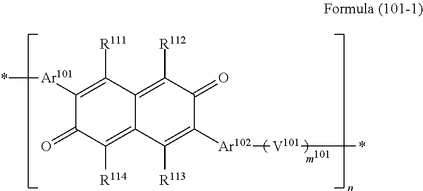
in Formula (101-1), each of R111 to R114 independently represents a hydrogen atom or a substituent; each of Ar101 and Ar102 independently represents a heteroarylene group or an arylene group; V101 represents a divalent linking group; m101 represents an integer of 0 to 6; when m101 is equal to or greater than 2, two or more groups represented by V101 may be the same as or different from each other; and n is equal to or greater than 2; and
in Formula (101-2), Cy101 represents a benzene ring, a naphthalene ring, or an anthracene ring; each of R115 to R118 independently represents a hydrogen atom or a substituent; each of Ar103 and Ar104 independently represents a heteroarylene group or an arylene group; V102 represents a divalent linking group; p101 represents an integer of 0 to 6; when p101 is equal to or greater than 2, two or more groups represented by V102 may be the same as or different from each other; and n is equal to or greater than 2.
[2] The organic film transistor described in [1] preferably containing a compound, which is composed of n repeating units represented by the following Formula (1-1) or (1-2), in the semiconductor active layer.
In Formula (1-1), each of R11 to R14 independently represents a hydrogen atom or a substituent; each of Ar1 and Ar2 independently represents a heteroarylene group or an arylene group; V1 represents a divalent linking group; m represents an integer of 0 to 6; when m is equal to or greater than 2, two or more groups represented by V1 may be the same as or different from each other; and n is equal to or greater than 2; and
in Formula (1-2), Cy represents a benzene ring, a naphthalene ring, or an anthracene ring; each of R15 to R18 independently represents a hydrogen atom or a substituent; each of Ar3 and Ar4 independently represents a heteroarylene group or an arylene group; V2 represents a divalent linking group; p represents an integer of 0 to 6; when p is equal to or greater than 2, two or more groups represented by V2 may be the same as or different from each other; and n is equal to or greater than 2.
[3] The organic film transistor described in [1] or [2], in which the compound composed of n repeating units represented by Formula (1-2) is preferably a compound composed of n repeating units represented by the following Formula (2-1), (2-2), (2-3), (2-4), or (2-5).
In Formulae (2-1) to (2-5), each of R15 to R18 and R21 to R42 independently represents a hydrogen atom or a substituent; each of Ar3 and Ar4 independently represents a heteroarylene group or an arylene group; V2 represents a divalent linking group; p represents an integer of 0 to 6; when p is equal to or greater than 2, two or more groups represented by V2 may be the same as or different from each other; and n is equal to or greater than 2.
[4] The organic film transistor described in [1] preferably containing a compound, which is composed of n repeating units represented by the following Formula (101-1) or (101-2), in the semiconductor active layer;
in Formula (101-1), each of R111 to R114 independently represents a hydrogen atom or a substituent; each of Ar101 and Ar102 independently represents a heteroarylene group or an arylene group; V101 represents a divalent linking group; m101 represents an integer of 0 to 6; when m101 is equal to or greater than 2, two or more groups represented by V101 may be the same as or different from each other; and n is equal to or greater than 2; and
in Formula (101-2), Cy101 represents a benzene ring, a naphthalene ring, or an anthracene ring; each of R115 to R118 independently represents a hydrogen atom or a substituent; each of Ar103 and Ar104 independently represents a heteroarylene group or an arylene group; V102 represents a divalent linking group; p101 represents an integer of 0 to 6; when p101 is equal to or greater than 2, two or more groups represented by V102 may be the same as or different from each other; and n is equal to or greater than 2.
[5] The organic film transistor described in [1] or [4], in which the compound composed of n repeating units represented by Formula (101-2) is preferably a compound composed of n repeating units represented by the following Formula (102-1), (102-2), (102-3), (102-4), or (102-5);
in Formulae (102-1) to (102-5), each of R115 to R118 and R121 to R142 independently represents a hydrogen atom or a substituent; each of Ar103 and Ar104 independently represents a heteroarylene group or an arylene group; V102 represents a divalent linking group; p101 represents an integer of 0 to 6; when p101 is equal to or greater than 2, two or more groups represented by V102 may be the same as or different from each other; and n is equal to or greater than 2.
[6] The organic film transistor described in any one of [1] to [5], in which in Formulae (1-1), (1-2), (2-1) to (2-5), (101-1), (101-2), and (102-1) to (102-5), each of V1, V2, V101, and V102 is independently preferably a divalent linking group represented by any of the following Formulae (V-1) to (V-17).
In Formulae (V-1) to (V-17), * represents a position where the divalent linking group is bonded to any of Ar1 to Ar4 and Ar101 to Ar104 when m, m101, p, or p101 is 1, and represents a position where the divalent linking group is bonded to any of Ar1 to Ar4, Ar101 to Ar104, and the divalent linking groups represented by Formulae (V-1) to (V-17) when m, m101, p, or p101 is equal to or greater than 2; each R in Formulae (V-1), (V-2), (V-5), (V-6), (V-9) to (V-11), (V-13) to (V-15), and (V-17) independently represents a hydrogen atom or an alkyl group; the groups adjacent to each other represented by R may form a ring by being bonded to each other; each Z in Formulae (V-4), (V-7), (V-8), and (V-12) independently represents a hydrogen atom, an alkyl group, or an alkoxy group; the groups adjacent to each other represented by Z may form a ring by being bonded to each other; each Y in Formula (V-16) independently represents a hydrogen atom, an alkyl group, an alkoxy group, a CN group, or a F atom; and the groups adjacent to each other represented by Y may form a ring by being bonded to each other.
[7] The organic film transistor described in [6], in which in Formulae (1-1), (1-2), (2-1) to (2-5), (101-1), (101-2), and (102-1) to (102-5), each of V1, V2, V101, and V102 is independently preferably a divalent linking group represented by any of Formulae (V-1) to (V-8) and (V-11) to (V-15).
[8] The organic film transistor described in any one of [1] to [7], in which in Formulae (1-1), (1-2), (2-1) to (2-5), (101-1), (101-2), and (102-1) to (102-5), each of Ar1 to Ar4 and Ar101 to Ar104 is independently preferably a divalent linking group represented by the following Formula (4-1), (4-2) or (4-3).
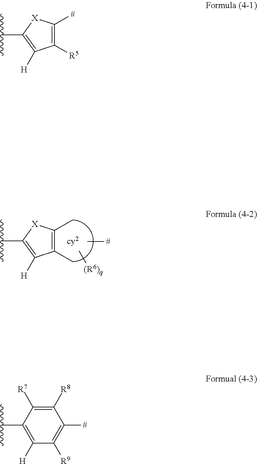
In Formulae (4-1) to (4-3), X represents a S atom, an O atom, or a Se atom; Cy2 represents a structure in which 1 to 4 rings are condensed; each of R5 to R9 independently represents a hydrogen atom or a substituent; q represents an integer of 0 to 6; when q is equal to or greater than 2, two or more groups represented by R6 may be the same as or different from each other; the wavy line represents a position where the divalent linking group is bonded to a cyclohexadienone ring-condensed site; and #represents a position where the divalent linking group is bonded to V1, V2, V101, or V102.
[9] The organic film transistor described in [8], in which in Formulae (1-1), (1-2), (2-1) to (2-5), (101-1), (101-2), and (102-1) to (102-5), each of Ar1 to Ar4 and Ar101 to Ar104 is independently preferably a divalent linking group represented by Formula (4-1) or (4-2).
[10] The organic film transistor described in [8] or [9], in which the divalent linking group represented by Formula (4-2) is preferably a divalent linking group represented by any of the following Formulae (5-1) to (5-8).
In Formulae (5-1) to (5-8), each R6 independently represents a hydrogen atom or a substituent; two or more groups represented by R6 may be the same as or different from each other; the wavy line represents a position where the divalent linking group is bonded to a cyclohexadienone ring-condensed site; and #represents a position where the divalent linking group is bonded to V1, V2, V101, or V102.
[11] The organic film transistor described in any one of [1] to [10], in which each of at least one of R11 to R14 in Formula (1-1), at least one of R15 to R18 in Formula (1-2), at least one of R15 to R18, R21, and R22 in Formula (2-1), at least one of R15 to R18 and R23 to R26 in Formula (2-2), at least one of R15 to R18 and R27 to R32 in Formula (2-3), at least one of R15 to R18 and R33 to R36 in Formula (2-4), at least one of R15 to R18 and R37 to R42 in Formula (2-5), at least one of R111 to R114 in Formula (101-1), at least one of R115 to R118 in Formula (101-2), at least one of R115 to R118, R121, and R122 in Formula (102-1), at least one of R115 to R118 and R123 to R126 in Formula (102-2), at least one of R115 to R118 and R127 to R132 in Formula (102-3), at least one of R115 to R118 and R133 to R136 in Formula (102-4), and at least one of R115 to R118 and R137 to R142 in Formula (102-5) is preferably a group represented by the following Formula (W).
-L-R Formula (W)
In Formula (W), L represents a divalent linking group represented by any of the following Formulae (L-1) to (L-12) or a divalent linking group formed by bonding of two or more divalent linking groups represented by any of the following Formulae (L-1) to (L-12); R represents a substituted or unsubstituted alkyl group, an oligo-oxyethylene group in which a repetition number v of an oxyethylene unit is equal to or greater than 2, an oligosiloxane group having two or more silicon atoms, or a substituted or unsubstituted silyl group; and R represents a substituted or unsubstituted silyl group only when L adjacent to R is a divalent linking group represented by any of the following Formulae (L-1) to (L-3);
in Formulae (L-1) to (L-12), the portion of a wavy line represents a position where the divalent linking group is bonded to a cyclohexadienone skeleton; * represents a position where the divalent linking group is bonded to any of the divalent linking groups represented by Formulae (L-1) to (L-12) and R; m in Formula (L-10) is 4; m in Formulae (L-11) and (L-12) is 2; and each R′ in Formulae (L-1), (L-2), (L-10), (L-11), and (L-12) independently represents a hydrogen atom or a substituent.
[12] The organic film transistor described in [11], in which in Formula (W), L is preferably a divalent linking group represented by any of Formulae (L-1), (L-4), and (L-8) or a divalent linking group formed by bonding of two or more divalent linking groups described above.
[13] The organic film transistor described in any one of [1] to [12], in which in Formulae (1-1), (1-2), (2-1) to (2-5), (101-1), (101-2), and (102-1) to (102-5), each n is independently preferably equal to or greater than 10.
[14]A compound composed of n repeating units represented by the following Formula (1-1), (1-2), (101-1), or (101-2);
in Formula (1-1), each of R11 to R14 independently represents a hydrogen atom or a substituent; each of Ar1 and Ar2 independently represents a heteroarylene group or an arylene group; V1 represents a divalent linking group; m represents an integer of 0 to 6; when m is equal to or greater than 2, two or more groups represented by V1 may be the same as or different from each other; and n is equal to or greater than 2;
in Formula (1-2), Cy represents a benzene ring, a naphthalene ring, or an anthracene ring; each of R15 to R18 independently represents a hydrogen atom or a substituent; each of Ar3 and Ar4 independently represents a heteroarylene group or an arylene group; V2 represents a divalent linking group; p represents an integer of 0 to 6; when p is equal to or greater than 2, two or more groups represented by V2 may be the same as or different from each other; and n is equal to or greater than 2;
in Formula (101-1), each of R111 to R114 independently represents a hydrogen atom or a substituent; each of Ar101 and Ar102 independently represents a heteroarylene group or an arylene group; V101 represents a divalent linking group; m101 represents an integer of 0 to 6; when m101 is equal to or greater than 2, two or more groups represented by V101 may be the same as or different from each other; and n is equal to or greater than 2; and
in Formula (101-2), Cy101 represents a benzene ring, a naphthalene ring, or an anthracene ring; each of R115 to R118 independently represents a hydrogen atom or a substituent; each of Ar103 and Ar104 independently represents a heteroarylene group or an arylene group; V102 represents a divalent linking group; p101 represents an integer of 0 to 6; when p101 is equal to or greater than 2, two or more groups represented by V102 may be the same as or different from each other; and n is equal to or greater than 2.
[15] The compound described in [14] that is preferably a compound composed of n repeating units represented by the following Formula (1-1) or (1-2).
In Formula (1-1), each of R11 to R14 independently represents a hydrogen atom or a substituent; each of Ar1 and Ar2 independently represents a heteroarylene group or an arylene group; V1 represents a divalent linking group; m represents an integer of 0 to 6; when m is equal to or greater than 2, two or more groups represented by V1 may be the same as or different from each other; and n is equal to or greater than 2; and Formula (1-2)
in Formula (1-2), Cy represents a benzene ring, a naphthalene ring, or an anthracene ring; each of R15 to R18 independently represents a hydrogen atom or a substituent; each of Ar3 and Ar4 independently represents a heteroarylene group or an arylene group; V2 represents a divalent linking group; p represents an integer of 0 to 6; when p is equal to or greater than 2, two or more groups represented by V2 may be the same as or different from each other; and n is equal to or greater than 2.
[16] The compound described in [14] or [15], in which the compound composed of n repeating units represented by Formula (1-2) is preferably a compound composed of n repeating units represented by the following Formula (2-1), (2-2), (2-3), (2-4), or (2-5).
In Formulae (2-1) to (2-5), each of R15 to R18 and R21 to R42 independently represents a hydrogen atom or a substituent; each of Ar3 and Ar4 independently represents a heteroarylene group or an arylene group; V2 represents a divalent linking group; p represents an integer of 0 to 6; when p is equal to or greater than 2, two or more groups represented by V2 may be the same as or different from each other; and n is equal to or greater than 2.
[17] The compound described in [14] that is preferably a compound composed of n repeating units represented by the following Formula (101-1) or (101-2);
in Formula (101-1), each of R111 to R114 independently represents a hydrogen atom or a substituent; each of Ar101 and Ar102 independently represents a heteroarylene group or an arylene group; V101 represents a divalent linking group; m101 represents an integer of 0 to 6; when m101 is equal to or greater than 2, two or more groups represented by V101 may be the same as or different from each other; and n is equal to or greater than 2; and
in Formula (101-2), Cy101 represents a benzene ring, a naphthalene ring, or an anthracene ring; each of R115 to R118 independently represents a hydrogen atom or a substituent; each of Ar103 and Ar104 independently represents a heteroarylene group or an arylene group; V102 represents a divalent linking group; p101 represents an integer of 0 to 6; when p101 is equal to or greater than 2, two or more groups represented by V102 may be the same as or different from each other; and n is equal to or greater than 2.
[18] The compound described in [14] or [17], in which the compound composed of n repeating units represented by Formula (101-2) is preferably a compound composed of n repeating units represented by the following Formula (102-1), (102-2), (102-3), (102-4), or (102-5);
in Formulae (102-1) to (102-5), each of R115 to R118 and R121 to R142 independently represents a hydrogen atom or a substituent; each of Ar103 and Ar104 independently represents a heteroarylene group or an arylene group; V102 represents a divalent linking group; p11 represents an integer of 0 to 6; when p101 is equal to or greater than 2, two or more groups represented by V102 may be the same as or different from each other; and n is equal to or greater than 2.
[19] The compound described in any one of [14] to [18], in which in Formulae (1-1), (1-2), (2-1) to (2-5), (101-1), (101-2), and (102-1) to (102-5), each of V1, V2, V101, and V102 is independently preferably a divalent linking group represented by any of the following Formulae (V-1) to (V-17).
In Formulae (V-1) to (V-17), * represents a position where the divalent linking group is bonded to any of Ar1 to Ar4 and Ar101 to Ar104 when m, m101, p, or p101 is 1, and represents a position where the divalent linking group is bonded to any of Ar1 to Ar4, Ar101 to Ar104, and the divalent linking groups represented by Formulae (V-1) to (V-17) when m, m101, p, or p101 is equal to or greater than 2; each R in Formulae (V-1), (V-2), (V-5), (V-6), (V-9) to (V-11), (V-13) to (V-15), and (V-17) independently represents a hydrogen atom or an alkyl group; the groups adjacent to each other represented by R may form a ring by being bonded to each other; each Z in Formulae (V-4), (V-7), (V-8), and (V-12) independently represents a hydrogen atom, an alkyl group, or an alkoxy group; the groups adjacent to each other represented by Z may form a ring by being bonded to each other; each Y in Formula (V-16) independently represents a hydrogen atom, an alkyl group, an alkoxy group, a CN group, or a F atom; and the groups adjacent to each other represented by Y may form a ring by being bonded to each other.
[20] The compound described in [19], in which in Formulae (1-1), (1-2), (2-1) to (2-5), (101-1), (101-2), and (102-1) to (102-5), each of V1, V2, V101, and V102 is independently preferably a divalent linking group represented by any of Formulae (V-1) to (V-8) and (V-11) to (V-15).
[21] The compound described in any one of [14] to [20], in which in Formulae (1-1), (1-2), (2-1) to (2-5), (101-1), (101-2), and (102-1) to (102-5), each of Ar1 to Ar4 and Ar101 to Ar104 is independently preferably a divalent linking group represented by the following Formula (4-1), (4-2), or (4-3).
In Formulae (4-1) to (4-3), X represents a S atom, an O atom, or a Se atom; Cy2 represents a structure in which 1 to 4 rings are condensed; each of R5 to R9 independently represents a hydrogen atom or a substituent; q represents an integer of 0 to 6; when q is equal to or greater than 2, two or more groups represented by R6 may be the same as or different from each other; the wavy line represents a position where the divalent linking group is bonded to a cyclohexadienone ring-condensed site; and #represents a position where the divalent linking group is bonded to V1, V2, V101, or V102.
[22] The compound described in [21], in which in Formulae (1-1), (1-2), (2-1) to (2-5), (101-1), (101-2), and (102-1) to (102-5), each of Ar1 to Ar4 and Ar101 to Ar104 is independently preferably a divalent linking group represented by Formula (4-1) or (4-2).
[23] The compound described in [21] or [22], in which the divalent linking group represented by Formula (4-2) is preferably a divalent linking group represented by any of the following Formulae (5-1) to (5-8).
In Formulae (5-1) to (5-8), each R6 independently represents a hydrogen atom or a substituent; two or more groups represented by R6 may be the same as or different from each other; the wavy line represents a position where the divalent linking group is bonded to a cyclohexadienone ring-condensed site; and #represents a position where the divalent linking group is bonded to V1, V2, V101, or V102.
[24] The compound described in any one of [14] to [23], in which each of at least one of R11 to R14 in Formula (1-1), at least one of R15 to R18 in Formula (1-2), at least one of R5 to R18, R21, and R22 in Formula (2-1), at least one of R15 to R18 and R23 to R26 in Formula (2-2), at least one of R15 to R18 and R27 to R32 in Formula (2-3), at least one of R15 to R18 and R33 to R36 in Formula (2-4), at least one of R15 to R18 and R37 to R42 in Formula (2-5), at least one of R111 to R114 in Formula (101-1), at least one of R115 to R118 in Formula (101-2), at least one of R115 to R118, R121, and R122 in Formula (102-1), at least one of R115 to R118 and R123 to R126 in Formula (102-2), at least one of R115 to R118 and R127 to R132 in Formula (102-3), at least one of R115 to R118 and R133 to R136 in Formula (102-4), and at least one of R115 to R118 and R137 to R142 in Formula (102-5) is preferably a group represented by the following Formula (W).
-L-R Formula (W)
In Formula (W), L represents a divalent linking group represented by any of the following Formulae (L-1) to (L-12) or a divalent linking group formed by bonding of two or more divalent linking groups represented by any of the following Formulae (L-1) to (L-12); R represents a substituted or unsubstituted alkyl group, an oligo-oxyethylene group in which a repetition number v of an oxyethylene unit is equal to or greater than 2, an oligosiloxane group having two or more silicon atoms, or a substituted or unsubstituted silyl group; and R represents a substituted or unsubstituted silyl group only when L adjacent to R is a divalent linking group represented by any of the following Formulae (L-1) to (L-3);
in Formulae (L-1) to (L-12), the portion of a wavy line represents a position where the divalent linking group is bonded to a cyclohexadienone skeleton; * represents a position where the divalent linking group is bonded to any of the divalent linking groups represented by Formulae (L-1) to (L-12) and R; m in Formula (L-10) is 4; m in Formulae (L-11) and (L-12) is 2; and each R′ in Formulae (L-1), (L-2), (L-10), (L-11), and (L-12) independently represents a hydrogen atom or a substituent.
[25] The compound described in [24], in which in Formula (W), L is preferably a divalent linking group represented by any of Formulae (L-1), (L-4), and (L-8) or a divalent linking group formed by bonding of two or more divalent linking groups described above.
[26] The compound described in any one of [14] to [25], in which in Formulae (1-1), (1-2), (2-1) to (2-5), (101-1), (101-2), and (102-1) to (102-5), each n is independently preferably equal to or greater than 10.
[27]A composition containing the compound described in any one of [14] to [26] and an organic solvent.
[28] The composition described in [27], in which the organic solvent is preferably an aromatic hydrocarbon-based solvent, an ether-based solvent, or a ketone-based solvent.
[29] An organic semiconductor material for a non-light-emitting organic semiconductor device, containing the compound described in any one of [14] to [26] or the composition described in [27] or [28].
[30]A material for an organic film transistor, containing the compound described in any one of [14] to [26] or the composition described in [27] or [28].
[31]A coating solution for a non-light-emitting organic semiconductor device, containing the compound described in any one of [14] to [26] or the composition described in [27] or [28].
[32]A coating solution for a non-light-emitting organic semiconductor device, containing the compound described in any one of [14] to [26] or the composition described in [27] or [28] and a polymer binder.
[33] An organic semiconductor film for a non-light-emitting organic semiconductor device, containing the compound described in any one of [14] to [26] or the composition described in [27] or [28].
[34] An organic semiconductor film for a non-light-emitting organic semiconductor device, containing the compound described in any one of [14] to [26] or the composition described in [27] or [28] and a polymer binder.
[35] The organic semiconductor film for a non-light-emitting organic semiconductor device described in [33] or [34] that is preferably prepared by a solution coating method.
According to the present invention, it is possible to provide a compound, which results in high carrier mobility when being used in a semiconductor active layer of an organic film transistor and exhibits high solubility in an organic solvent, and an organic film transistor which uses the compound.
BRIEF DESCRIPTION OF THE DRAWINGS
FIG. 1 is a schematic view showing the cross-section of an exemplary structure of an organic film transistor of the present invention.
FIG. 2 is a schematic view showing the cross-section of a structure of an organic film transistor manufactured as a substrate for measuring FET characteristics in examples of the present invention.
DESCRIPTION OF THE PREFERRED EMBODIMENTS
Hereinafter, the present invention will be specifically descried. The following constituents are described based on typical embodiments or specific examples in some cases, but the present invention is not limited to such embodiments. In the present specification, a range of numerical values represented by using “to” means a range which includes the numerical values listed before and after “to” as a lower limit and an upper limit.
In the present invention, in a case in which hydrogen atoms are used in describing each formula without being particularly differentiated from each other, the hydrogen atoms include isotopes (a deuterium atom and the like). Furthermore, atoms constituting a substituent also include isotopes thereof.
In the present specification, a compound composed of n repeating units represented by Formula (X) has the same definition as a compound represented by Formula (X) (X is any number or letter). In Formulae (1-1), (1-2), (2-1) to (2-5), (101-1), (101-2), and (102-1) to (102-5), a terminal (for example, represented by *) other than n repeating units represents a linking group linked to a hydrogen atom or a substituent. In the compound composed of n repeating units represented by any of Formulae (1-1), (1-2), (2-1) to (2-5), (101-1), (101-2), and (102-1) to (102-5), * on a molecular terminal may be a hydrogen atom or any substituent, and the molecular terminal is preferably a hydrogen atom, a trialkyltin group, a halogen atom, a perfluoroalkanesulfonyloxy group, —B(OH)2, —B(ORX)2, a trialkylsilyl group, an aryl group, a heteroaryl group, or the like. Herein, RX represents an alkyl group, and a plurality of alkyl groups represented by RX may form a ring by being bonded to each other.
[Organic Film Transistor]
The organic film transistor of the present invention contains a compound, which is represented by the following Formula (1-1), (1-2), (101-1), or (101-2), in a semiconductor active layer.
In Formula (1-1), each of R11 to R14 independently represents a hydrogen atom or a substituent; each of Ar1 and Ar2 independently represents a heteroarylene group or an arylene group; V1 represents a divalent linking group; m represents an integer of 0 to 6; when m is equal to or greater than 2, two or more groups represented by V1 may be the same as or different from each other; and n is equal to or greater than 2;
in Formula (1-2), Cy represents a benzene ring, a naphthalene ring, or an anthracene ring; each of R15 to R18 independently represents a hydrogen atom or a substituent; each of Ar3 and Ar4 independently represents a heteroarylene group or an arylene group; V2 represents a divalent linking group; p represents an integer of 0 to 6; when p is equal to or greater than 2, two or more groups represented by V2 may be the same as or different from each other; and n is equal to or greater than 2;
in Formula (101-1), each of R111 to R114 independently represents a hydrogen atom or a substituent; each of Ar101 and Ar102 independently represents a heteroarylene group or an arylene group; V101 represents a divalent linking group; m101 represents an integer of 0 to 6; when m101 is equal to or greater than 2, two or more groups represented by V101 may be the same as or different from each other; and n is equal to or greater than 2; and
in Formula (101-2), Cy101 represents a benzene ring, a naphthalene ring, or an anthracene ring; each of R115 to R118 independently represents a hydrogen atom or a substituent; each of Ar103 and Ar104 independently represents a heteroarylene group or an arylene group; V102 represents a divalent linking group; p101 represents an integer of 0 to 6; when p101 is equal to or greater than 2, two or more groups represented by V102 may be the same as or different from each other; and n is equal to or greater than 2.
A first preferred embodiment of the organic film transistor of the present invention contains the compound represented by Formula (1-1) or (1-2) in the semiconductor active layer.
A second preferred embodiment of the organic film transistor of the present invention contains the compound represented by Formula (101-1) or (101-2) in the semiconductor active layer.
When being used in the semiconductor active layer of the organic film transistor, the compound composed of n repeating units represented by Formula (1-1), (1-2), (101-1), or (101-2) results in high carrier mobility and exhibits high solubility in an organic solvent. Therefore, by containing the compound in the semiconductor layer, the organic film transistor of the present invention exhibits high carrier mobility.
In the compound composed of n repeating units represented by Formula (1-1), (1-2), (101-1), or (101-2), a ring-condensed cyclohexadienone skeleton has a carbonyl group, and thus the overlapping of HOMO sufficiently occurs. Accordingly, an organic film transistor having high carrier mobility can be obtained. Furthermore, the compound brings about an effect of obtaining unexpectedly high solubility in an organic solvent. Such an effect is considered to be obtained by the following mechanism. The compound composed of n repeating units represented by Formula (1-1), (1-2), (101-1), or (101-2) has a hydrogen bond between a double-bonded oxygen atom of the ring-condensed cyclohexadienone skeleton, which will be a mother skeleton, and a hydrogen atom of arylene groups or heteroarylene groups adjacent to each other on both sides of the ring-condensed cyclohexadienone skeleton. In a film, the hydrogen bond is maintained, and thus the planarity is improved. As a result, the distance between polymer molecules is shortened, and hence the carrier mobility can be improved. In a solution, the hydrogen bond is dissociated and freely rotates, and thus the solubility in an organic solvent can be improved.
Conventionally, a polycyclic ring-condensed compound having an aromatic heterocyclic ring is known to be useful as an organic EL element material. However, the usefulness of the compound as an organic EL element material does not necessarily mean that the compound is also useful as a semiconductor material for an organic film transistor. This is because the characteristics required for an organic compound vary between the organic EL element and the organic film transistor. Generally, in the organic EL element, a charge needs to be transported in the film thickness direction (usually, several nm to hundreds of nm) of the film. In contrast, in the organic film transistor, a charge (carrier) needs to be transported through a long distance between electrodes (usually, several μm to hundreds of m) in the film surface direction, and hence extremely high carrier mobility is required. Therefore, as the semiconductor material for an organic film transistor, an organic compound which has high regularity of molecular arrangement and high crystallinity is required. Furthermore, in order to achieve high carrier mobility, a π conjugation plane is preferably perpendicular to a substrate. In contrast, in the organic EL element, in order to improve light emitting efficiency, an element which has high light emitting efficiency and uniformly emits light within a plane is required. Generally, an organic compound having high crystallinity results in defectiveness in emitting light, such as uneven field intensity within a plane, uneven light emission, and emission quenching. Accordingly, as the material for an organic EL element, a material which has low crystallinity and high amorphousness is desirable. Therefore, even if an organic compound constituting the organic EL element material is directly used as the organic semiconductor material, excellent transistor characteristics are not necessarily obtained.
In addition, it is preferable that the organic film transistor of the present invention using the compound composed of n repeating units represented by Formula (1-1), (1-2), (101-1), or (101-2) shows a slight threshold voltage shift after repeated driving. In order to make the organic film transistor show a slight threshold voltage shift after repeated driving, HOMO of the organic semiconductor material needs not to be too shallow or too deep. Furthermore, the chemical stability (particularly, resistance against air oxidation and stability against oxidation and reduction) of the organic semiconductor material, the heat stability of the film state, the high film density which makes it difficult for air or moisture to permeate the film, the film quality in which the film has small defectiveness such that charge accumulation does not easily occur, and the like are required. Regarding an oligomer or a polymer compound having repeating units just like the compound composed of n repeating units represented by Formula (1-1), (1-2), (101-1), or (101-2), the higher the solubility of the compound in an organic solvent at the time of forming a film, the smaller the threshold voltage shift after repeated driving can be reduced when the compound is used in the semiconductor active layer of the organic film transistor. It is considered that because the compound composed of n repeating units represented by Formula (1-1), (1-2), (101-1), or (101-2) satisfies the aforementioned requirements, the organic film transistor shows a slight threshold voltage shift after repeated driving. That is, in the organic film transistor showing a slight threshold voltage shift after repeated driving, the semiconductor active layer has high chemical resistance, high film density, and the like, and thus the organic film transistor can effectively function as a transistor over a long period of time.
Hereinafter, preferred embodiments of the compound of the present invention, the organic film transistor of the present invention, and the like will be described.
<Compound Composed of n Repeating Units Represented by Formula (1-1), (1-2), (101-1), or (101-2)>
The compound of the present invention is composed of n repeating units represented by Formula (1-1), (1-2), (101-1), or (101-2). The compound of the present invention is contained in a semiconductor active layer, which will be described later, in the organic film transistor of the present invention. That is, the compound of the present invention can be used as a material for an organic film transistor.
Hereinafter, the compound composed of n repeating units represented by Formula (1-1), (1-2), (101-1), or (101-2) will be described.
<<Compound Composed of n Repeating Units Represented by Formula (1-1)>>
The compound composed of n repeating units represented by Formula (1-1) is represented by the following formula.
(In Formula (1-1), each of R11 to R14 independently represents a hydrogen atom or a substituent; each of Ar1 and Ar2 independently represents a heteroarylene group or an arylene group; V1 represents a divalent linking group; m represents an integer of 0 to 6; when m is equal to or greater than 2, two or more groups represented by V1 may be the same as or different from each other; and n is equal to or greater than 2.)
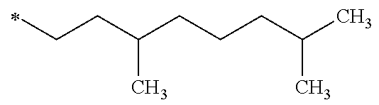
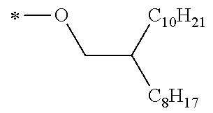
In Formula (1-1), each of R11 to R14 independently represents a hydrogen atom or a substituent. Examples of the substituent that each of R11 to R14 can independently adopt include a halogen atom, an alkyl group (including an alkyl group having 1 to 40 carbon atoms such as a methyl group, an ethyl group, a propyl group, a butyl group, a pentyl group, a hexyl group, a heptyl group, an octyl group, a nonyl group, a decyl group, an undecyl group, a dodecyl group, a tridecyl group, a tetradecyl group, or a pentadecyl group (preferably an alkyl group having 3 to 40 carbon atoms and more preferably an alkyl group having 10 to 30 carbon atoms), a 2,6-dimethyloctyl group, a 2-decyltetradecyl group, a 2-hexyldodecyl group, a 2-ethyloctyl group, a 2-decyltetradecyl group, a 2-butyldecyl group, a 1-octylnonyl group, a 2-ethyloctyl group, a 2-octyltetradecyl group, and the like), an alkenyl group (including a 1-pentenyl group, a cycloalkenyl group, a bicycloalkenyl group, and the like), an alkynyl group (including a 1-pentynyl group, a trimethylsilylethynyl group, a triethylsilylethynyl group, a tri-i-propylsilylethynyl group, a 2-p-propylphenylethynyl group, and the like), an aryl group (including an aryl group having 6 to 20 carbon atoms such as a phenyl group, a naphthyl group, a p-pentylphenyl group, a 3,4-dipentylphenyl group, a p-heptoxyphenyl group, a 3,4-diheptoxyphenyl group, and the like), a hetero ring group (may also be referred to as a heterocyclic group, including a 2-hexylfuranyl group and the like), a cyano group, a hydroxyl group, a nitro group, an acyl group (including a hexanoyl group, a benzoyl group, and the like), an aryloxy group, a silyloxy group, a heterocyclic oxy group, an acyloxy group, a carbamoyloxy group, an amino group (including an anilino group), an acylamino group, an aminocarbonylamino group (including a ureide group), an alkoxy group (including an alkoxy group having 1 to 40 carbon atoms such as a methoxy group, an ethoxy group, a propoxy group, a butoxy group, a pentoxy group, a hexyloxy group, a heptoxy group, an octoxy group, a nonyloxy group, a decyloxy group, a 2-hexyldecyloxy group, an undecyloxy group, a dodecyloxy group, a tridecyloxy group, a tetradecyloxy group, and a pentadecyloxy group (preferably an alkoxy group having 3 to 40 carbon atoms and more preferably an alkoxy group having 10 to 30 carbon atoms)), an aryloxycarbonylamino group, alkyl and aryl sulfonylamino groups, a mercapto group, alkyl and arylthio groups (including a methylthio group, an octylthio group, and the like), a heterocyclic thio group, a sulfamoyl group, a sulfo group, alkyl and aryl sulfinyl groups, alkyl and aryl sulfonyl groups, alkyloxy and aryloxy carbonyl groups, a carbamoyl group, an arylazo group, a heterocyclic azo group, an imide group, a phosphino group, a phosphinyl group, a phosphinyloxy group, a phosphinylamino group, a phosphono group, a silyl group (a ditrimethylsiloxy methylbutoxy group), a hydrazino group, a group represented by Formula (W) which will be described later, and other known substituents.
These substituents may further have a substituent.
In addition, these substituents may have a group derived from a polymerizable group.
Each of R11 and R13 is independently preferably any of a hydrogen atom, an alkyl group, an aryl group, an alkenyl group, an alkynyl group, a heterocyclic group, an alkoxy group, an alkylthio group, and a group represented by Formula (W) which will be described later, more preferably any of a hydrogen atom, an alkyl group having 1 to 12 carbon atoms, and an alkoxy group having 1 to 11 carbon atoms, particularly preferably any of a hydrogen atom, an alkyl group having 1 to 3 carbon atoms, and an alkoxy group having 1 to 3 carbon atoms from the viewpoint of making it possible to easily form an intramolecular hydrogen bond by keeping a cyclohexadienone skeleton and arylene groups or a heteroarylene groups (Ar1 to Ar4) adjacent to each other on both sides of the cyclohexadienone skeleton within a plane by means of suppressing the bulkiness of R11 and R13, more particularly preferably any of a hydrogen atom, a methyl group, and an ethoxy group, and most preferably a hydrogen atom.
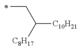
Each of R12 and R14 is independently preferably any of a hydrogen atom, an alkyl group, an aryl group, an alkenyl group, an alkynyl group, an alkoxy group, a heterocyclic group, an alkylthio group, an amino group, and a group represented by Formula (W) which will be described later, more preferably any of a hydrogen atom, an alkyl group having 3 to 40 carbon atoms, an aryl group having 6 to 20 carbon atoms, an alkenyl group having 2 to 12 carbon atoms, an alkynyl group having 2 to 12 carbon atoms, an alkoxy group having 3 to 40 carbon atoms, a heterocyclic group having 5 to 12 carbon atoms, an alkylthio group having 1 to 12 carbon atoms, an amino group substituted with an alkyl group having 1 to 12 carbon atoms, and a group represented by Formula (W) which will be described later, and particularly preferably a group represented by Formula (W) which will be described later. Furthermore, each of R12 and R14 is preferably a branched substituent in which a linear substituent further has a substituent.
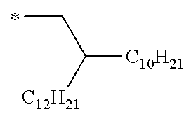
The alkyl group which can be adopted as R12 and R14 is preferably an alkyl group having 3 to 40 carbon atoms, more preferably an alkyl group having 10 to 30 carbon atoms from the viewpoint of the chemical stability and the carrier transport properties, and particularly preferably an alkyl group having 15 to 30 carbon atoms. Furthermore, the alkyl group which can be adopted as R12 and R14 is preferably a linear or branched alkyl group, and more preferably a branched alkyl group from the viewpoint of improving the carrier mobility and the solubility without deteriorating the intramolecular hydrogen bonding properties.
The alkoxy group which can be adopted as R12 and R14 is preferably an alkoxy group having 3 to 40 carbon atoms, more preferably an alkoxy group having 10 to 30 carbon atoms from the viewpoint of the chemical stability and the carrier transport properties, and particularly preferably an alkoxy group having 15 to 30 carbon atoms. Furthermore, the alkoxy group which can be adopted as R12 and R14 is preferably a linear or branched alkoxy group, and more preferably a branched alkoxy group from the viewpoint of improving the carrier mobility and the solubility without deteriorating the intramolecular hydrogen bonding properties.
At least one of R11 to R14 is preferably a group represented by the following Formula (W).
-L-R Formula (W)
(In Formula (W), L represents a divalent linking group represented by any of the following Formulae (L-1) to (L-12) or a divalent linking group formed by bonding of two or more divalent linking groups represented by any of the following Formulae (L-1) to (L-12); R represents a substituted or unsubstituted alkyl group, an oligo-oxyethylene group in which a repetition number v of an oxyethylene unit is equal to or greater than 2, an oligosiloxane group having two or more silicon atoms, or a substituted or unsubstituted silyl group; and R represents a substituted or unsubstituted silyl group only when L adjacent to R is a divalent linking group represented by any of the following Formulae (L-1) to (L-3).)
(In Formulae (L-1) to (L-12), the portion of a wavy line represents a position where the divalent linking group is bonded to a cyclohexadienone skeleton; * represents a position where the divalent linking group is bonded to any of the divalent linking groups represented by Formulae (L-1) to (L-12) and R; m in Formula (L-10) is 4; m in Formulae (L-11) and (L-12) is 2; and each R′ in Formulae (L-1), (L-2), (L-10), (L-11), and (L-12) independently represents a hydrogen atom or a substituent.)
In Formula (W), L represents a divalent linking group represented by any of the following Formulae (L-1) to (L-12) or a divalent linking group formed by bonding of two or more divalent linking groups represented by any of Formulae (L-1) to (L-12). When L forms a linking group in which divalent linking groups represented by any of Formula (L-1) to (L-12) are bonded to each other, the number of the bonded divalent linking groups represented by any of Formula (L-1) to (L-12) is preferably 2 to 4, and more preferably 2 or 3.
Each substituent R′ in Formulae (L-1), (L-2), (L-10), (L-11), and (L-12) independently represents a hydrogen atom or a substituent. Examples of the substituent which can be adopted as R′ include an alkyl group having 5 to 15 carbon atoms (preferably an alkyl group having 6 to 15 carbon atoms) and an alkoxy group having 5 to 15 carbon atoms (preferably an alkoxy group having 6 to 15 carbon atoms).
m in Formula (L-10) represents 4, and m in Formulae (L-11) and (L-12) represents 2.
L is preferably a divalent linking group represented by any of Formulae (L-1), (L-4), and (L-8) or a divalent linking group formed by bonding of two or more divalent linking groups described above, more preferably a divalent linking group represented by any of Formula (L-1) and (L-4) or a divalent linking group formed by bonding of two or more divalent linking groups described above, and particularly preferably a divalent linking group represented by Formula (L-1) or a divalent linking group formed by bonding of two or more divalent linking groups described above.
In Formula (W), R represents a hydrogen atom, a substituted or unsubstituted alkyl group, an oligo-oxyethylene group in which a repetition number of an oxyethylene unit is equal to or greater than 2, an oligosiloxane group having two or more silicon atoms, or a substituted or unsubstituted silyl group. Here, R represents a substituted or unsubstituted silyl group only when L adjacent to R is a divalent linking group represented by Formula (L-3), and represents a hydrogen atom only when L adjacent to R is a divalent linking group represented by any of Formulae (L-1) to (L-3).
When L is represented by Formula (L-1), the substituted or unsubstituted alkyl group which can be adopted as R is preferably an alkyl group having 3 or more carbon atoms, more preferably an alkyl group having 3 to 40 carbon atoms, even more preferably an alkyl group having 10 to 30 carbon atoms from the viewpoint of the chemical stability and the carrier transport properties, and particularly preferably an alkyl group having 15 to 30 carbon atoms. Furthermore, when L is represented by Formula (L-1), the substituted or unsubstituted alkyl group which can be adopted as R is preferably a linear or branched alkyl group, and more preferably a branched alkyl group from the viewpoint of improving the carrier mobility and the solubility without deteriorating the intramolecular hydrogen bonding properties.
When L is represented by any of Formulae (L-2) and (L-3), the alkyl group which can be adopted as R is preferably an alkyl group having 2 or more carbon atoms, preferably an alkyl group having 3 to 18 carbon atoms, even more preferably an alkyl group having 3 to 12 carbon atoms, and particularly preferably an alkyl group having 4 to 10 carbon atoms.
When L is represented by any of Formulae (L-4) to (L-12), the alkyl group which can be adopted as R is preferably an alkyl group having 4 or more carbon atoms, preferably an alkyl group having 4 to 18 carbon atoms, even more preferably an alkyl group having 4 to 12 carbon atoms, and particularly preferably an alkyl group having 4 to 10 carbon atoms.
When -L-R in Formula (W) contains an alkyl group, if the alkyl group represented by R is equal to or greater than the lower limit of the aforementioned range, the carrier mobility is improved. Furthermore, when L contains Formula (L-1) adjacent to R, if the number of carbon atoms of the alkyl group formed by bonding of the alkylene group represented by Formula (L-1) and the alkyl group represented by R is equal to or greater than the lower limit of the aforementioned range, the carrier mobility is improved.
When R is an alkyl group having a substituent, examples of the substituent include a halogen atom and the like, and as the halogen atom, a fluorine atom is preferable. When R is an alkyl group having a fluorine-atom, a perfluoroalkyl group may be formed by substituting all the hydrogen atoms of the alkyl group with fluorine atoms.
In the present specification, when R is an oligo-oxyethylene group in which a repetition number v of an oxyethylene group is equal to or greater than 2, the “oxyethylene group” represented by R is a group represented by —(CH2CH2)vOY (the repetition number v of an oxyethylene unit represents an integer of equal to or greater than 2, and Y on the terminal represents a hydrogen atom or a substituent). When Y on the terminal of the oligo-oxyethylene group is a hydrogen atom, the terminal becomes a hydroxy group. The repetition number v of an oxyethylene unit is preferably 2 to 4, and more preferably 2 or 3. It is preferable that the hydroxy group on the terminal of the oligo-oxyethylene group is blocked. That is, Y preferably represents a substituent. In this case, the hydroxy group is preferably blocked by an alkyl group having 1 to 3 carbon atoms. That is, Y is preferably an alkyl group having 1 to 3 carbon atoms, more preferably a methyl group or an ethyl group, and particularly preferably a methyl group.
When R is an oligosiloxane group having 2 or more silicon atoms, the repetition number of the siloxane unit is preferably 2 to 4, and more preferably 2 or 3. Furthermore, the Si atom is preferably bonded to a hydrogen atom or an alkyl group. When the Si atom is bonded to an alkyl group, the number of carbon atoms of the alkyl group is preferably 1 to 3. For example, the Si atom is preferably bonded to a methyl group or an ethyl group. The Si atom may be bonded to the same alkyl groups or may be bonded to different alkyl groups or hydrogen atoms. The siloxane units constituting the oligosiloxane group may be the same as or different from each other, but it is preferable that they are the same as each other. When R is a substituted or unsubstituted silyl group, as the silyl group which can be adopted as R, a trialkylsilyl group having 3 to 15 carbon atoms is preferable.
Examples of the group represented by Formula (W) include a 2,6-dimethyloctyl group, a 3,7-dimethyloctyl group, a 2-decyltetradecyl group, a 2-hexyldecyl group, a 2-hexyldodecyl group, a 2-ethyloctyl group, a 2-decyltetradecyl group, a 2-butyldecyl group, a 2-octylnonyl group, a 2-octyldodecyl group, a 2-octyltetradecyl group, a 2-ethylhexyl group, a 2-butylnonyl group, a 2-hexyldecyloxy group, a ditrimethylsiloxy methylbutoxy group, a butoxy group, a hexyl group, a heptyl group, an octyl group, a nonyl group, a decyl group, an undecyl group, a dodecyl group, a tridecyl group, a tetradecyl group, a pentadecyl group, a 3,7-dimethyloctyloxy group, a 2-decyltetradecyloxy group, a 2-hexyldecyloxy group, a 2-hexyldodecyloxy group, a 2-ethyloctyloxy group, a 2-decyltetradecyloxy group, a 2-butyldecyloxy group, a 2-octyldodecyloxy group, a 2-octyltetradecyloxy group, a 2-ethylhexyloxy group, a hexyloxy group, a heptyloxy group, an octyloxy group, a nonyloxy group, a decyloxy group, an undecyloxy group, a dodecyloxy group, a tridecyloxy group, a tetradecyloxy group, a pentadecyloxy group, and the like.
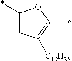
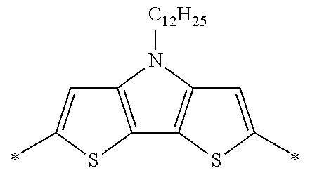
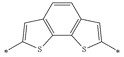
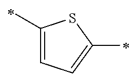
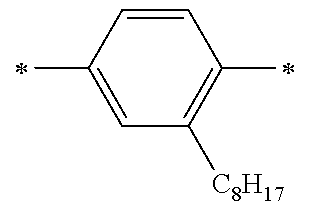
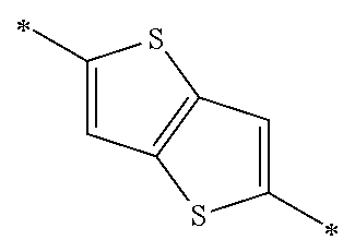
Each of Ar1 and Ar2 independently represents a heteroarylene group or an arylene group. From the viewpoint of improving the carrier mobility by improving the intramolecular hydrogen bonding properties, it is preferable that Ar1 and R11 do not form a condensed ring by being bonded to each other. Furthermore, from the viewpoint of improving the carrier mobility by improving the intramolecular hydrogen bonding properties, it is preferable that Ar2 and R13 do not form a condensed ring by being bonded to each other. The heteroarylene group or the arylene group which can be adopted as Ar1 and Ar2 is not particularly limited, and examples thereof include a heteroarylene group having 4 to 30 carbon atoms and an arylene group having 6 to 30 carbon atoms. The heteroarylene group or the arylene group which can be adopted as Ar1 and Ar2 is preferably a divalent linking group represented by the following Formula (4-1), (4-2), or (4-3), and more preferably a divalent linking group represented by the following Formula (4-1) or (4-2). Furthermore, it is preferable that Ar1 and Ar2 represent the same heteroarylene groups or arylene groups.
(In Formulae (4-1) to (4-3), X represents a S atom, an O atom, or a Se atom; Cy2 represents a structure in which 1 to 4 rings are condensed; each of R5 to R9 independently represents a hydrogen atom or a substituent; q represents an integer of 0 to 6; when q is equal to or greater than 2, two or more groups represented by R6 may be the same as or different from each other; the wavy line represents a position where the divalent linking group is bonded to a cyclohexadienone ring-condensed site; and #represents a position where the divalent linking group is bonded to V1 or V2.)
In Formulae (4-1) to (4-3), X represents a S atom, an O atom, or a Se atom. X is preferably a S atom or a Se atom, and more preferably a S atom.
In Formulae (4-1) to (4-3), each of R5 to R9 independently represents a hydrogen atom or a substituent. The substituent which can be adopted as R5 to R9 is not particularly limited, and examples thereof include the same substituents as the substituents which can be adopted as R11 to R14.
The alkyl group which can be adopted as R5 to R9 is more preferably an alkyl group having 3 to 40 carbon atoms, even more preferably an alkyl group having 10 to 30 carbon atoms from the viewpoint of the chemical stability and the carrier transport properties, and particularly preferably an alkyl group having 15 to 30 carbon atoms. Furthermore, the alkyl group which can be adopted as R5 to R9 is preferably a linear or branched alkyl group, and more preferably a branched alkyl group from the view point of improving the carrier mobility and the solubility without deteriorating the intramolecular hydrogen bonding properties.
The alkoxy group which can be adopted as R5 to R9 is more preferably an alkoxy group having 3 to 40 carbon atoms, even more preferably an alkoxy group having 10 to 30 carbon atoms from the viewpoint of the chemical stability and the carrier transport properties, and particularly preferably an alkoxy group having 15 to 30 carbon atoms. Furthermore, the alkoxy group which can be adopted as R5 to R9 is preferably a linear or branched alkoxy group, and more preferably a branched alkoxy group from the viewpoint of improving the carrier mobility and the solubility without deteriorating the intramolecular hydrogen bonding properties.
These substituents may further have a substituent.
In addition, these substituents may have a group derived from a polymerizable group.
In Formula (4-2), q represents an integer of 0 to 6. q is preferably an integer of 0 to 3, more preferably an integer of 0 to 2, and even more preferably an integer of 0 or 1.
In Formula (4-2), Cy2 represents a structure in which 1 to 4 rings are condensed. Cy2 is preferably a structure in which 1 to 4 aromatic rings or heterocyclic aromatic rings are condensed, more preferably a structure in which 1 to 4 aromatic rings having 6 to 10 carbon atoms or 1 to 4 heterocyclic aromatic rings having 4 to 6 carbon atoms are condensed, and particularly preferably a structure in which 1 to 4 benzene rings or thiophene rings are condensed.
The divalent linking group represented by Formula (4-2) is preferably a divalent linking group represented by any of the following Formulae (5-1) to (5-8), and more preferably a divalent linking group represented by Formula (5-1).
(In Formulae (5-1) to (5-8), each R6 independently represents a hydrogen atom or a substituent; two or more groups represented by R6 may be the same as or different from each other; the wavy line represents a position where the divalent linking group is bonded to a cyclohexadienone ring-condensed site; and #represents a position where the divalent linking group is bonded to V1 or V2.)
In Formulae (5-1) to (5-8), each R6 independently represents a hydrogen atom or a substituent, and two or more groups represented by R6 may be the same as or different from each other. Examples of the substituent which can be adopted as R6 include those exemplified above as substituents which can be adopted as R5 to R9 in Formulae (4-1) to (4-3), and the preferred range thereof is also the same.
In Formula (1-1), V1 represents a divalent linking group. From the viewpoint of improving the solubility, it is preferable that V1 does not form a condensed ring by being bonded to Ar1 or Ar2. The divalent linking group which can be adopted as V1 is not particularly limited, but is preferably represented by any of the following Formulae (V-1) to (V-17).
(In Formulae (V-1) to (V-17), * represents a position where the divalent linking group is bonded to any of Ar1 to Ar4 when m or p is 1, and represents a position where the divalent linking group is bonded to any of Ar1 to Ar4 and the divalent linking groups represented by Formulae (V-1) to (V-17) when m or p is equal to or greater than 2; each R in Formulae (V-1), (V-2), (V-5), (V-6), (V-9) to (V-11), (V-13) to (V-15), and (V-17) independently represents a hydrogen atom or an alkyl group; the groups adjacent to each other represented by R may form a ring by being bonded to each other; each Z in Formulae (V-4), (V-7), (V-8), and (V-12) independently represents a hydrogen atom, an alkyl group, or an alkoxy group; the groups adjacent to each other represented by Z may form a ring by being bonded to each other; each Y in Formula (V-16) independently represents a hydrogen atom, an alkyl group, an alkoxy group, a CN group, or a F atom; and the groups adjacent to each other represented by Y may form a ring by being bonded to each other.)
Each R in Formulae (V-1), (V-2), (V-5), (V-6), (V-9) to (V-11), (V-13) to (V-15), and (V-17) independently represents a hydrogen atom or an alkyl group, and the groups adjacent to each other represented by R may form a ring by being bonded to each other. Examples of the alkyl group which can be adopted as R include the alkyl group which can be adopted as R5 to R9 in Formulae (4-1) to (4-3). Furthermore, the preferred range of the alkyl group which can be adopted as R is the same as the preferred range of the alkyl group which can be adopted as R5 to R9.
Each Z in Formulae (V-4), (V-7), (V-8), and (V-12) independently represents a hydrogen atom, an alkyl group, or an alkoxy group, and the groups adjacent to each other represented by Z may form a ring by being bonded to each other. Examples of the alkyl group or the alkoxy group which can be adopted as Z include the alkyl group and the alkoxy group which can be adopted as R5 to R9 in Formulae (4-1) to (4-3). Furthermore, the preferred range of the alkyl group and the alkoxy group which can be adopted as Z is the same as the preferred range of the alkyl group and the alkoxy group which can be adopted as R5 to R9.
Each Y in Formula (V-16) independently represents a hydrogen atom, an alkyl group, an alkoxy group, a CN group, or a F atom, and the groups adjacent to each other represented by Y may form a ring by being bonded to each other. Y is preferably an alkyl group or an alkoxy group. Examples of the alkyl group or the alkoxy group which can be adopted as Y include the alkyl group and the alkoxy group exemplified above as the substituent which can be adopted as R5 to R9 in Formulae (4-1) to (4-3), and the preferred range thereof is also the same.
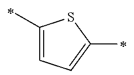
Among the divalent linking groups represented by Formulae (V-1) to (V-17), the divalent linking groups represented by Formulae (V-1) to (V-15) are preferable, the divalent linking groups represented by Formulae (V-1) to (V-8) and (V-11) to (V-15) are more preferable, and the divalent linking groups represented by Formulae (V-1) to (V-3) and (V-7) are particularly preferable.
In Formula (1-1), m represents an integer of 0 to 6. When m is equal to or greater than 2, two or more groups represented by V1 may be the same as or different from each other. m is preferably an integer of 0 to 5, and more preferably 0 to 3.
In Formula (1-1), n represents an integer of equal to or greater than 2. n is preferably equal to or greater than 5, more preferably equal to or greater than 10, and particularly preferably equal to or greater than 30. The greater the value of n, the further the interaction between π-conjugated polymer chains can be improved, and thus the carrier mobility can be improved. The upper limit of n is not particularly limited, but it is preferably equal to or less than 2,000 and more preferably equal to or less than 1,000.
<<Compound Composed of n Repeating Units Represented by Formula (1-2)>>
The compound composed of n repeating units represented by Formula (1-2) is represented by the following Formula.
(In Formula (1-2), Cy represents a benzene ring, a naphthalene ring, or an anthracene ring; each of R15 to R18 independently represents a hydrogen atom or a substituent; each of Ar3 and Ar4 independently represents a heteroarylene group or an arylene group; V2 represents a divalent linking group; p represents an integer of 0 to 6; when p is equal to or greater than 2, two or more groups represented by V2 may be the same as or different from each other; and n is equal to or greater than 2.)
In Formula (1-2), each of R15 to R18 independently represents a hydrogen atom or a substituent. The substituent which can be adopted as R15 and R17 is the same as the substituent which can be adopted as R11 and R13 in Formula (1-1), and the preferred range thereof is also the same. The substituent which can be adopted as R16 and R18 is the same as the substituent which can be adopted as R12 and R14 in Formula (1-1), and the preferred range thereof is also the same.
In Formula (1-2), each of Ar3 and Ar4 independently represents a heteroarylene group or an arylene group. From the viewpoint of improving the carrier mobility by improving the intramolecular hydrogen bonding properties, it is preferable that Ar3 and R15 do not form a condensed ring by being bonded to each other. In addition, from the viewpoint of improving the carrier mobility by improving the intramolecular hydrogen bonding properties, it is preferable that Ar4 and R17 do not form a condensed ring by being bonded to each other. The heteroarylene group or the arylene group which can be adopted as Ar3 and Ar4 is the same as the heteroarylene group or the arylene group which can be adopted as Ar1 and Ar2 in Formula (1-1), and the preferred range thereof is also the same.
In Formula (1-2), V2 represents a divalent linking group. From the viewpoint of improving the solubility, it is preferable that V2 does not form a condensed ring together with Ar3 or Ar4. The divalent linking group which can be adopted as V2 is the same as the divalent linking group which can be adopted as V1 in Formula (1-1), and the preferred range thereof is also the same. Here, when m or p is 1, * in Formulae (V-1) to (V-17) represents a position where the divalent linking group is bonded to any of Ar3 and Ar4, and when m or p is equal to or greater than 2, * in Formulae (V-1) to (V-17) represents a position where the divalent linking group is bonded to any of Ar3, Ar4, and the divalent linking groups represented by Formulae (V-1) to (V-17).
In Formula (1-2), p represents an integer of 0 to 6. When p is equal to or greater than 2, two or more groups represented by V2 may be the same as or different from each other. p has the same definition as m in Formula (1-1), and the preferred range thereof is also the same.
In Formula (1-2), n represents an integer of equal to or greater than 2. n has the same definition as n in Formula (1-1), and the preferred range thereof is also the same.
In Formula (1-2), Cy represents a benzene ring, a naphthalene ring, or an anthracene ring. The benzene ring, the naphthalene ring, or the anthracene ring represented by Cy may have a substituent, and the substituent is not particularly limited. The substituent is the same as the substituent which can be adopted as R12 and R14 in Formula (1-1), and the preferred range thereof is also the same. Here, from the viewpoint of improving the long-term stability of the compound, it is preferable that a hydroxyl group (—OH group) is not substituted.
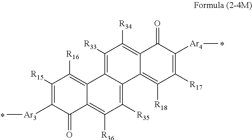
The site where the benzene ring, the naphthalene ring, and the anthracene ring represented by Cy are condensed with a cyclohexadienone ring is not particularly limited. Specifically, it is preferable that the benzene ring, the naphthalene ring, or the anthracene ring is condensed such that the compound composed of n repeating units represented by Formula (1-2) becomes a compound having a rotationally symmetric skeleton. It is more preferable that the benzene ring, the naphthalene ring, or the anthracene ring is condensed so as to form a compound composed of n repeating units represented by the following Formula (2-1), (2-2), (2-3), (2-4), or (2-5).
(In Formulae (2-1) to (2-5), each of R15 to R18 and R21 to R42 independently represents a hydrogen atom or a substituent; each of Ar3 and Ar4 independently represents a heteroarylene group or an arylene group; V2 represents a divalent linking group; p represents an integer of 0 to 6; when p is equal to or greater than 2, two or more groups represented by V2 may be the same as or different from each other; and n is equal to or greater than 2.)
In Formulae (2-1) to (2-5), each of R15 to R18 and R21 to R42 independently represents a hydrogen atom or a substituent.
The substituent which can be adopted as R15 to R18 in Formulae (2-1) to (2-5) is the same as the substituent which can be adopted as R15 to R18 in Formula (1-2), and the preferred range thereof is also the same.
The substituent which can be adopted as R21 to R42 in Formulae (2-1) to (2-5) is the same as the substituent which can be adopted as R12 and R14 in Formula (1-1), and the preferred range thereof is also the same.
It is preferable that at least one of R15 to R18, R21, and R22 in Formula (2-1) is a group represented by Formula (W). More preferably, at least two out of R16, R18, R21, and R22 are groups represented by Formula (W). Particularly preferably, both of R21 and R22 are groups represented by Formula (W).
It is preferable that at least one of R15 to R18 and R23 to R26 in Formula (2-2) is a group represented by Formula (W). More preferably, at least two out of R16, R18, R23, R24, R25, and R26 are groups represented by Formula (W). Particularly preferably, all of R23, R24, R25, and R26 are groups represented by Formula (W).
It is preferable that at least one of R15 to R18 and R27 to R32 in Formula (2-3) is a group represented by Formula (W). More preferably, at least two out of R16, R18, and R27 to R32 are groups represented by Formula (W). Particularly preferably, both of R28 and R31 are groups represented by Formula (W).
It is preferable that at least one of R15 to R18 and R33 to R36 in Formula (2-4) is a group represented by Formula (W). More preferably, zero to two out of R1 to R18 and two to four out of R33 to R36 are groups represented by Formula (W). Particularly preferably, two out of R15 to R18 and two out of R33 to R36 are groups represented by Formula (W).
It is preferable that at least one of R15 to R18 and R37 to R42 in Formula (2-5) is a group represented by Formula (W). More preferably, zero to two out of R15 to R18 and two to six out of R37 to R42 are groups represented by Formula (W). Particularly preferably, two out of R15 to R18 and two out of R37 to R42 are groups represented by Formula (W).
In Formulae (2-1) to (2-5), each of Ar3 and Ar4 independently represents a heterocyclic aromatic ring or an aromatic ring. The heteroarylene group or the arylene group which can be adopted as Ar3 and Ar4 is the same as the heteroarylene group or the arylene group which can be adopted as Ar3 and Ar4 in Formula (1-2), and the preferred range thereof is also the same.
In Formulae (2-1) to (2-5), V2 represents a divalent linking group. The divalent linking group which can be adopted as V2 is the same as the divalent linking group which can be adopted as V2 in Formula (1-2), and the preferred range thereof is also the same.
In Formulae (2-1) to (2-5), p represents an integer of 0 to 6. When p is equal to or greater than 2, two or more groups represented by V2 may be the same as or different from each other. p in Formulae (2-1) to (2-5) has the same definition as p in Formula (1-2), and the preferred range thereof is also the same.
In Formulae (2-1) to (2-5), n represents an integer of equal to or greater than 2. n has the same definition as n in Formula (1-2), and the preferred range thereof is also the same.
From the viewpoint of maintaining the balance between the extent of widening of a n plane and high solubility, the compound composed of n repeating units represented by Formula (1-2) is preferably a compound composed of n repeating units represented by Formula (2-1) or (2-2), and more preferably a compound composed of n repeating units represented by Formula (2-1).
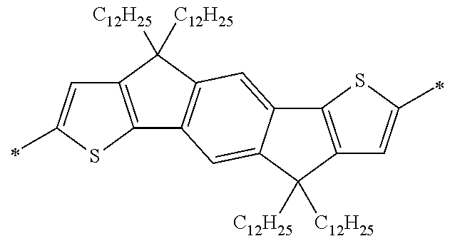
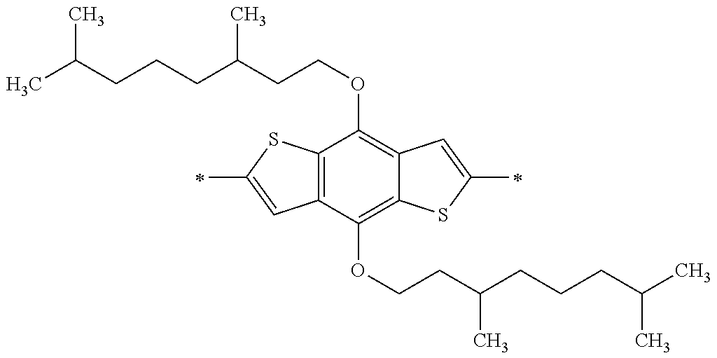
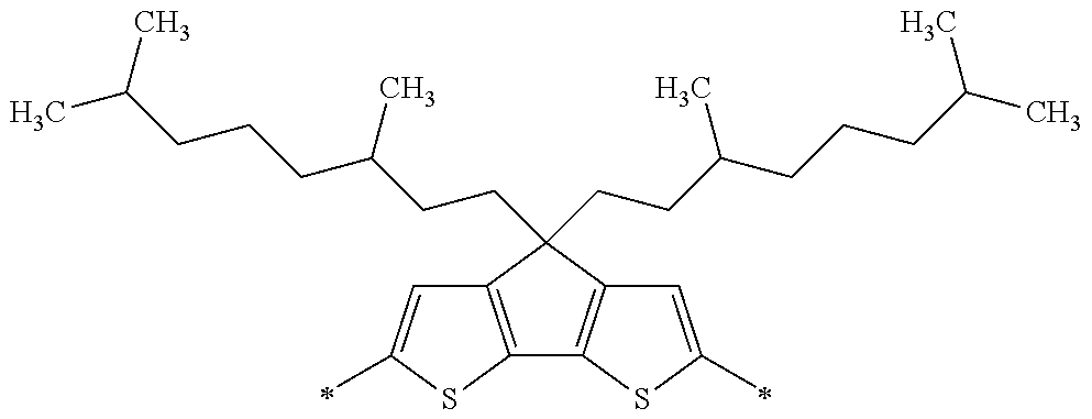
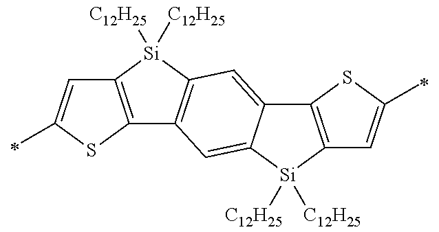
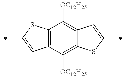
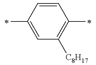
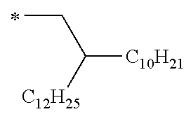
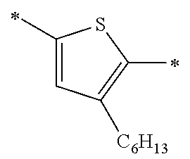
Specific examples of the compound composed of n repeating units represented by Formula (1-1) or (1-2) include a compound composed of n repeating units represented by the following Formula (MV). However, the compound composed of n repeating units represented by Formula (1-1) or 1-2) that can be used in the present invention is not limited to the specific example.
(In Formula (MV), M1 represents a divalent linking group M1 in the following table; Vx represents a divalent linking group Vx in the following table; and n represents an integer of equal to or greater than 2.)
| TABLE 1 |
| |
| Compound |
|
|
| No. |
M1 |
Vx |
| |
| |
| 1 |
1-1-1 |
V1 |
| 2 |
1-1-1 |
V8 |
| 3 |
1-1-1 |
V21 |
| 4 |
1-1-2 |
V3 |
| 5 |
1-1-2 |
V7 |
| 6 |
1-1-2 |
V23 |
| 7 |
1-1-3 |
V25 |
| 8 |
1-1-3 |
V26 |
| 9 |
1-1-3 |
V28 |
| 10 |
1-1-4 |
V15 |
| 11 |
1-1-4 |
V27 |
| 12 |
1-1-4 |
V33 |
| 13 |
1-1-5 |
V17 |
| 14 |
1-1-5 |
V31 |
| 15 |
1-1-5 |
V33 |
| 16 |
1-1-6 |
V14 |
| 17 |
1-1-6 |
V37 |
| 18 |
1-1-6 |
V40 |
| 19 |
1-1-7 |
V8 |
| 20 |
1-1-7 |
V44 |
| 21 |
1-1-8 |
V45 |
| 22 |
1-1-8 |
V46 |
| 23 |
1-1-9 |
V5 |
| 24 |
1-1-9 |
V48 |
| 25 |
1-1-10 |
V4 |
| 26 |
1-1-10 |
V18 |
| 27 |
1-1-10 |
V50 |
| 28 |
1-1-11 |
V14 |
| 29 |
1-1-11 |
V17 |
| 30 |
1-1-12 |
V18 |
| 31 |
1-1-12 |
V20 |
| 32 |
1-1-13 |
V16 |
| 33 |
1-1-13 |
V22 |
| 34 |
1-1-13 |
V41 |
| 35 |
1-1-14 |
V49 |
| 36 |
1-1-14 |
V47 |
| 37 |
1-1-15 |
V22 |
| 38 |
1-1-15 |
V23 |
| 39 |
1-1-16 |
V24 |
| 40 |
1-1-16 |
V27 |
| 41 |
1-1-17 |
V32 |
| 42 |
1-1-17 |
V36 |
| 43 |
1-1-18 |
V42 |
| 44 |
1-1-18 |
V47 |
| 45 |
1-1-19 |
V50 |
| 46 |
1-1-19 |
V10 |
| 47 |
1-1-20 |
V1 |
| 48 |
1-1-20 |
V3 |
| 49 |
1-1-20 |
V16 |
| 50 |
1-1-21 |
V4 |
| 51 |
1-1-21 |
V5 |
| 52 |
1-1-22 |
None |
| 53 |
1-1-22 |
V19 |
| 54 |
1-1-23 |
V18 |
| 55 |
1-1-23 |
V4 |
| 56 |
1-1-24 |
V2 |
| 57 |
1-1-24 |
V8 |
| 58 |
1-1-25 |
V3 |
| 59 |
1-1-25 |
None |
| 60 |
1-1-26 |
V1 |
| 61 |
1-1-26 |
V2 |
| 62 |
1-1-27 |
V3 |
| 63 |
1-1-27 |
V4 |
| 64 |
1-1-27 |
V36 |
| 65 |
1-1-28 |
V9 |
| 66 |
1-1-28 |
V13 |
| 67 |
1-1-28 |
V27 |
| 68 |
1-1-29 |
V2 |
| 69 |
1-1-29 |
V3 |
| 70 |
1-1-30 |
None |
| 71 |
1-1-30 |
V11 |
| 72 |
1-1-30 |
V37 |
| 73 |
1-1-31 |
V4 |
| 74 |
1-1-31 |
V47 |
| 75 |
1-1-32 |
V3 |
| 76 |
1-1-32 |
V5 |
| 77 |
1-1-33 |
V1 |
| 78 |
1-1-33 |
V8 |
| 79 |
1-1-34 |
V2 |
| 80 |
1-1-34 |
V7 |
| 81 |
1-1-35 |
V1 |
| 82 |
1-1-36 |
V12 |
| 83 |
1-1-37 |
V3 |
| 84 |
1-1-38 |
V47 |
| 85 |
1-1-39 |
V24 |
| 86 |
1-1-40 |
V38 |
| 87 |
1-1-41 |
V48 |
| 88 |
1-1-42 |
V30 |
| 89 |
1-1-43 |
V49 |
| 90 |
1-1-44 |
V48 |
| 91 |
1-1-45 |
V45 |
| 92 |
1-1-46 |
V5 |
| 93 |
1-1-47 |
V4 |
| 94 |
1-1-48 |
V23 |
| 95 |
1-1-48 |
V48 |
| 96 |
1-1-49 |
V7 |
| 97 |
1-1-49 |
V36 |
| 98 |
1-1-50 |
V5 |
| 99 |
2-1-1 |
V8 |
| 100 |
2-1-1 |
V20 |
| 101 |
2-1-1 |
V23 |
| 102 |
2-1-2 |
V7 |
| 103 |
2-1-2 |
V22 |
| 104 |
2-1-2 |
V44 |
| 105 |
2-1-3 |
V5 |
| 106 |
2-1-3 |
V28 |
| 107 |
2-1-3 |
V33 |
| 108 |
2-1-4 |
V6 |
| 109 |
2-1-4 |
V19 |
| 110 |
2-1-5 |
V15 |
| 111 |
2-1-5 |
V22 |
| 112 |
2-1-5 |
V33 |
| 113 |
2-1-6 |
V14 |
| 114 |
2-1-6 |
V4 |
| 115 |
2-1-6 |
V40 |
| 116 |
2-1-7 |
V32 |
| 117 |
2-1-7 |
V33 |
| 118 |
2-1-7 |
V36 |
| 119 |
2-1-8 |
V3 |
| 120 |
2-1-8 |
V20 |
| |
| TABLE 2 |
| |
| Compound |
|
|
| No. |
M1 |
Vx |
| |
| 121 |
2-1-9 |
V21 |
| 122 |
2-1-9 |
V23 |
| 123 |
2-1-9 |
V31 |
| 124 |
2-1-10 |
V25 |
| 125 |
2-1-10 |
V30 |
| 126 |
2-1-10 |
V50 |
| 127 |
2-1-11 |
V26 |
| 128 |
2-1-11 |
V27 |
| 129 |
2-1-12 |
V1 |
| 130 |
2-1-12 |
V21 |
| 131 |
2-1-13 |
V16 |
| 132 |
2-1-13 |
V22 |
| 133 |
2-1-13 |
V41 |
| 134 |
2-1-14 |
V26 |
| 135 |
2-1-14 |
V38 |
| 136 |
2-1-15 |
V5 |
| 137 |
2-1-15 |
V21 |
| 138 |
2-1-16 |
V23 |
| 139 |
2-1-16 |
V40 |
| 140 |
2-1-17 |
V43 |
| 141 |
2-1-17 |
V46 |
| 142 |
2-1-18 |
V32 |
| 143 |
2-1-18 |
V34 |
| 144 |
2-1-19 |
V5 |
| 145 |
2-1-19 |
V11 |
| 146 |
2-1-20 |
V4 |
| 147 |
2-1-20 |
V11 |
| 148 |
2-1-21 |
V3 |
| 149 |
2-1-21 |
V13 |
| 150 |
2-1-22 |
V1 |
| 151 |
2-1-22 |
V50 |
| 152 |
2-1-23 |
V19 |
| 153 |
2-1-23 |
V24 |
| 154 |
2-1-24 |
None |
| 155 |
2-1-24 |
V4 |
| 156 |
2-1-25 |
V2 |
| 157 |
2-1-25 |
V8 |
| 158 |
2-1-26 |
V1 |
| 159 |
2-1-26 |
V10 |
| 160 |
2-1-27 |
V6 |
| 161 |
2-1-27 |
V48 |
| 162 |
2-1-28 |
V3 |
| 163 |
2-1-28 |
V13 |
| 164 |
2-1-28 |
None |
| 165 |
2-1-29 |
V4 |
| 166 |
2-1-29 |
V38 |
| 167 |
2-1-30 |
V11 |
| 168 |
2-1-30 |
V24 |
| 169 |
2-1-30 |
V45 |
| 170 |
2-1-31 |
V1 |
| 171 |
2-1-32 |
V5 |
| 172 |
2-1-33 |
V8 |
| 173 |
2-1-34 |
None |
| 174 |
2-1-35 |
V12 |
| 175 |
2-1-36 |
V4 |
| 176 |
2-1-37 |
V3 |
| 177 |
2-1-38 |
V39 |
| 178 |
2-1-39 |
V49 |
| 179 |
2-1-40 |
V19 |
| 180 |
2-1-41 |
V3 |
| 181 |
2-1-42 |
V5 |
| 182 |
2-1-43 |
V2 |
| 183 |
2-1-44 |
V10 |
| 184 |
2-1-45 |
V3 |
| 185 |
2-1-46 |
V4 |
| 186 |
2-1-47 |
V5 |
| 187 |
2-1-48 |
V22 |
| 188 |
2-1-48 |
V30 |
| 189 |
2-1-49 |
V4 |
| 190 |
2-1-49 |
V42 |
| 191 |
2-1-50 |
V23 |
| 192 |
2-2-1 |
V22 |
| 193 |
2-2-2 |
V21 |
| 194 |
2-2-3 |
V5 |
| 195 |
2-2-4 |
V6 |
| 196 |
2-2-5 |
V3 |
| 197 |
2-2-6 |
V15 |
| 198 |
2-2-7 |
V43 |
| 199 |
2-2-8 |
V41 |
| 200 |
2-2-9 |
V33 |
| 201 |
2-2-10 |
V3 |
| 202 |
2-2-11 |
V13 |
| 203 |
2-2-12 |
V4 |
| 204 |
2-2-13 |
V2 |
| 205 |
2-2-14 |
V4 |
| 206 |
2-2-15 |
V38 |
| 207 |
2-2-16 |
V45 |
| 208 |
2-2-17 |
None |
| 209 |
2-2-18 |
V9 |
| 210 |
2-2-19 |
V21 |
| 211 |
2-2-20 |
V31 |
| 212 |
2-3-1 |
V20 |
| 213 |
2-3-2 |
V15 |
| 214 |
2-3-3 |
V35 |
| 215 |
2-3-4 |
V42 |
| 216 |
2-3-5 |
V29 |
| 217 |
2-3-6 |
V5 |
| 218 |
2-3-7 |
V22 |
| 219 |
2-3-8 |
V34 |
| 220 |
2-3-9 |
V40 |
| 221 |
2-3-10 |
V3 |
| 222 |
2-3-11 |
V13 |
| 223 |
2-3-12 |
V4 |
| 224 |
2-3-13 |
V12 |
| 225 |
2-3-14 |
V4 |
| 226 |
2-3-15 |
V3 |
| 227 |
2-3-16 |
V50 |
| 228 |
2-3-17 |
None |
| 229 |
2-3-18 |
V9 |
| 230 |
2-3-19 |
V20 |
| 231 |
2-3-20 |
V26 |
| 232 |
2-4-1 |
V22 |
| 233 |
2-4-2 |
V15 |
| 234 |
2-4-3 |
V34 |
| 235 |
2-4-4 |
V42 |
| 236 |
2-4-5 |
V29 |
| 237 |
2-4-6 |
V5 |
| 238 |
2-4-7 |
V20 |
| 239 |
2-4-8 |
V35 |
| 240 |
2-4-9 |
V41 |
| |
| TABLE 3 |
| |
| Compound |
|
|
| No. |
M1 |
Vx |
| |
| 241 |
2-4-10 |
V3 |
| 242 |
2-4-11 |
V13 |
| 243 |
2-4-12 |
V4 |
| 244 |
2-4-13 |
V12 |
| 245 |
2-4-14 |
None |
| 246 |
2-4-15 |
V3 |
| 247 |
2-4-16 |
V49 |
| 248 |
2-4-17 |
V2 |
| 249 |
2-4-18 |
V9 |
| 250 |
2-4-19 |
V21 |
| 251 |
2-4-20 |
V25 |
| 252 |
2-5-1 |
V20 |
| 253 |
2-5-2 |
V15 |
| 254 |
2-5-3 |
V35 |
| 255 |
2-5-4 |
V42 |
| 256 |
2-5-5 |
V29 |
| 257 |
2-5-6 |
V5 |
| 258 |
2-5-7 |
V22 |
| 259 |
2-5-8 |
V34 |
| 260 |
2-5-9 |
V40 |
| 261 |
2-5-10 |
V3 |
| 262 |
2-5-11 |
V13 |
| 263 |
2-5-12 |
V4 |
| 264 |
2-5-13 |
V12 |
| 265 |
2-5-14 |
None |
| 266 |
2-5-15 |
V3 |
| 267 |
2-5-16 |
V50 |
| 268 |
2-5-17 |
V2 |
| 269 |
2-5-18 |
V9 |
| 270 |
2-5-19 |
V20 |
| 271 |
2-5-20 |
V26 |
| |
In the above tables, M1 represents a linking group represented by the following Formula (1-1M), (2-1M), (2-2M), (2-3M), (2-4M), or (2-5M), and Vx represents linking groups V1 to V50 which will be described later.
In Formula (1-1M), each of Ar1, Ar2, and R11 to R14 represents the following groups.
| TABLE 4 |
| |
| |
Ar1 |
Ar2 |
R11 |
R12 |
| |
| 1-1-1 |
|
|
H |
H |
| |
| 1-1-2 |
|
|
H |
|
| |
| 1-1-3 |
|
|
H |
|
| |
| 1-1-4 |
|
|
*—CH3 |
|
| |
| 1-1-5 |
|
|
H |
|
| |
| 1-1-6 |
|
|
H |
*—OC8H13 |
| |
| 1-1-7 |
|
|
*—C8H17 |
H |
| |
| 1-1 -8 |
|
|
H |
|
| |
| 1-1-9 |
|
|
H |
|
| |
| 1-1-10 |
|
|
H |
|
| |
| |
|
R13 |
R14 |
| |
| |
1-1-1 |
H |
H |
| |
| |
1-1-2 |
H |
|
| |
| |
1-1-3 |
H |
|
| |
| |
1-1-4 |
*—CH3 |
|
| |
| |
1-1-5 |
H |
|
| |
| |
1-1-6 |
H |
*—OC8H13 |
| |
1-1-7 |
*—C8H17 |
H |
| |
| |
1-1 -8 |
H |
|
| |
| |
1-1-9 |
H |
|
| |
| |
1-1-10 |
H |
|
| |
| TABLE 5 |
| |
| |
Ar1 |
Ar2 |
R11 |
R12 |
| |
| 1-1-11 |
|
|
H |
|
| |
| 1-1-12 |
|
|
*—OEt |
|
| |
| 1-1-13 |
|
|
H |
*—OEt |
| |
| 1-1-14 |
|
|
H |
*—SC6H13 |
| |
| 1-1-15 |
|
|
H |
H |
| |
| 1-1-16 |
|
|
H |
|
| |
| 1-1-17 |
|
|
H |
|
| |
| 1-1-18 |
|
|
*—CH3 |
|
| |
| 1-1-19 |
|
|
H |
|
| |
| 1-1-20 |
|
|
H |
|
| |
| |
|
R13 |
R14 |
| |
| |
1-1-11 |
H |
|
| |
| |
1-1-12 |
*—OEt |
|
| |
| |
1-1-13 |
H |
*—OEt |
| |
1-1-14 |
H |
*—SC6H13 |
| |
1-1-15 |
H |
H |
| |
| |
1-1-16 |
H |
|
| |
| |
1-1-17 |
H |
|
| |
| |
1-1-18 |
*—CH3 |
|
| |
| |
1-1-19 |
H |
|
| |
| |
1-1-20 |
H |
|
| |
| TABLE 6 |
| |
| |
Ar1 |
AR2 |
R11 |
R12 |
| |
| 1-1-21 |
|
|
H |
|
| 1-1-22 |
|
|
H |
H |
| |
| 1-1-23 |
|
|
H |
|
| |
| 1-1-24 |
|
|
H |
*—C6H13 |
| |
| 1-1-25 |
|
|
*—C6H13 |
*—OEt |
| |
| 1-1-26 |
|
|
H |
|
| |
| 1-1-27 |
|
|
H |
H |
| |
| |
|
R13 |
R14 |
| |
| |
1-1-21 |
H |
|
| |
| |
1-1-22 |
H |
H |
| |
| |
1-1-23 |
H |
|
| |
| |
1-1-24 |
H |
*—C6H13 |
| |
1-1-25 |
*—C6H13 |
*—OEt |
| |
| |
1-1-26 |
H |
|
| |
1-1-27 |
H |
H |
| |
| TABLE 7 |
| |
| |
Ar1 |
Ar2 |
| |
| 1-1-28 |
|
|
| |
| 1-1-29 |
|
|
| |
| 1-1-30 |
|
|
| |
| 1-1-31 |
|
|
| |
| 1-1-32 |
|
|
| |
| 1-1-33 |
|
|
| |
| 1-1-34 |
|
|
| |
| |
|
R11 |
R12 |
R13 |
R14 |
| |
| |
1-1-28 |
H |
*—C8H17 |
H |
*—C8H17 |
| |
1-1-29 |
H |
*—OC6H13 |
H |
*—OC6H13 |
| |
| |
1-1-30 |
*—CH3 |
|
*—CH3 |
|
| |
| |
1-1-31 |
H |
|
H |
|
| |
| |
1-1-32 |
H |
|
H |
|
| |
| |
1-1-33 |
H |
|
H |
|
| |
| |
1-1-34 |
*—CH3 |
H |
*—CH3 |
H |
| |
| TABLE 8 |
| |
| |
Ar1 |
Ar2 |
| |
| 1-1-35 |
|
|
| |
| 1-1-36 |
|
|
| |
| 1-1-37 |
|
|
| |
| 1-1-38 |
|
|
| |
| 1-1-39 |
|
|
| |
| 1-1-40 |
|
|
| |
| 1-1-41 |
|
|
| |
| 1-1-42 |
|
|
| |
| |
|
R11 |
R12 |
R13 |
R14 |
| |
| |
1-1-35 |
H |
H |
H |
H |
| |
1-1-36 |
H |
*—OC6H13 |
H |
*—OC6H13 |
| |
| |
1-1-37 |
H |
|
H |
|
| |
| |
1-1-38 |
H |
H |
H |
H |
| |
| |
1-1-39 |
H |
|
H |
|
| |
| |
1-1-40 |
*—CH3 |
|
*—CH3 |
|
| |
| |
1-1-41 |
*—C6H13 |
Et |
*—C6H13 |
Et |
| |
1-1-42 |
H |
*—C6H13 |
H |
*—C6H13 |
| |
| TABLE 9 |
| |
| |
Ar1 |
| |
| 1-1-43 |
|
| |
| 1-1-44 |
|
| |
| 1-1-45 |
|
| |
| 1-1-46 |
|
| |
| 1-1-47 |
|
| |
| 1-1-48 |
|
| |
| 1-1-49 |
|
| |
| 1-1-50 |
|
| |
| |
Ar2 |
| |
| 1-1-43 |
|
| |
| 1-1-44 |
|
| |
| 1-1-45 |
|
| |
| 1-1-46 |
|
| |
| 1-1-47 |
|
| |
| 1-1-48 |
|
| |
| 1-1-49 |
|
| |
| 1-1-50 |
|
| |
| |
R11 |
R12 |
R13 |
| |
| 1-1-43 |
H |
*—OC6H13 |
H |
| |
| 1-1-44 |
H |
|
H |
| |
| 1-1-45 |
H |
*—C12H25 |
H |
| 1-1-46 |
H |
H |
H |
| |
| 1-1-47 |
H |
|
H |
| |
| 1-1-48 |
H |
|
H |
| |
| 1-1-49 |
*—OEt |
|
*—OEt |
| |
| 1-1-50 |
H |
|
H |
| |
| |
|
R14 |
| |
| |
1-1-43 |
*—OC6H13 |
| |
| |
1-1-44 |
|
| |
| |
1-1-45 |
*—C12H25 |
| |
1-1-46 |
H |
| |
| |
1-1-47 |
|
| |
| |
1-1-48 |
|
| |
| |
1-1-49 |
|
| |
| |
1-1-50 |
|
| |
In Formula (2-1M), each of Ar3, Ar4, R15 to R18, R21, and R22 represents the following groups.
| TABLE 10 |
| |
| |
Ar3 |
Ar4 |
R15 |
R16 |
R17 |
| |
| 2-1-1 |
|
|
H |
H |
H |
| |
| 2-1-2 |
|
|
H |
H |
H |
| |
| 2-1-3 |
|
|
H |
|
H |
| |
| 2-1-4 |
|
|
*—CH3 |
Et |
*—CH3 |
| |
| 2-1-5 |
|
|
H |
H |
H |
| |
| 2-1-6 |
|
|
H |
|
H |
| |
| 2-1-7 |
|
|
H |
*—OEt |
H |
| |
| 2-1-8 |
|
|
H |
|
H |
| |
| 2-1-9 |
|
|
H |
|
H |
| |
| 2-1-10 |
|
|
H |
|
H |
| |
| |
|
R18 |
R21 |
R22 |
| |
| |
2-1-1 |
H |
|
|
| |
| |
2-1-2 |
H |
|
|
| |
| |
2-1-3 |
|
H |
H |
| |
| |
2-1-4 |
Et |
|
|
| |
| |
2-1-5 |
H |
|
|
| |
| |
2-1-6 |
|
H |
H |
| |
| |
2-1-7 |
*—OEt |
|
|
| |
| |
2-1-8 |
|
|
|
| |
| |
2-1-9 |
|
|
|
| |
| |
2-1-10 |
|
|
|
| |
| TABLE 11 |
| |
| |
Ar3 |
Ar4 |
R15 |
R16 |
R17 |
| |
| 2-1-11 |
|
|
H |
H |
H |
| |
| 2-1-12 |
|
|
H |
H |
H |
| |
| 2-1-13 |
|
|
H |
|
H |
| |
| 2-1-14 |
|
|
H |
*—SC6H13 |
H |
| |
| 2-1-15 |
|
|
H |
H |
H |
| |
| 2-1-16 |
|
|
H |
|
H |
| |
| 2-1-17 |
|
|
H |
|
H |
| |
| 2-1-18 |
|
|
*—CH3 |
|
*—CH3 |
| |
| 2-1-19 |
|
|
H |
|
H |
| |
| 2-1-20 |
|
|
H |
|
H |
| |
| |
|
R18 |
R21 |
R22 |
| |
| |
2-1-11 |
H |
|
|
| |
| |
2-1-12 |
H |
|
|
| |
| |
2-1-13 |
|
H |
H |
| |
| |
2-1-14 |
*—SC6H13 |
H |
H |
| |
| |
2-1-15 |
H |
|
|
| |
| |
2-1-16 |
|
|
|
| |
| |
2-1-17 |
|
H |
H |
| |
| |
2-1-18 |
|
*—C12H25 |
*—C12H25 |
| |
| |
2-1-19 |
|
H |
H |
| |
| |
2-1-20 |
|
H |
H |
| |
| TABLE 12 |
| |
| |
Ar3 |
Ar4 |
R15 |
R16 |
R17 |
| |
| 2-1-21 |
|
|
H |
H |
H |
| |
| 2-1-22 |
|
|
H |
|
H |
| |
| 2-1-23 |
|
|
H |
|
H |
| |
| 2-1-24 |
|
|
H |
*—C6H13 |
H |
| |
| 2-1-25 |
|
|
H |
H |
H |
| |
| 2-1-26 |
|
|
*—CH3 |
|
*—CH3 |
| |
| 2-1-27 |
|
|
H |
H |
H |
| |
| |
|
R18 |
R21 |
R22 |
| |
| |
2-1-21 |
H |
|
|
| |
| |
2-1-22 |
|
|
|
| |
| |
2-1-23 |
|
|
|
| |
| |
2-1-24 |
*—C6H13 |
H |
H |
| |
| |
2-1-25 |
H |
|
|
| |
| |
2-1-26 |
|
H |
H |
| |
| |
2-1-27 |
H |
H |
H |
| |
| TABLE 13 |
| |
| |
Ar3 |
Ar4 |
R15 |
| |
| 2-1-28 |
|
|
H |
| |
| 2-1-29 |
|
|
H |
| |
| 2-1-30 |
|
|
H |
| |
| 2-1-31 |
|
|
H |
| |
| 2-1-32 |
|
|
H |
| |
| 2-1-33 |
|
|
H |
| |
| 2-1-34 |
|
|
H |
| |
| |
|
R16 |
R17 |
R18 |
R21 |
R22 |
| |
| |
2-1-28 |
*—C8H17 |
H |
*—C8H17 |
*—C8H17 |
*—C8H17 |
| |
2-1-29 |
*—OC6H13 |
H |
*—OC6H13 |
*—OC6H13 |
*—OC6H13 |
| |
| |
2-1-30 |
|
H |
|
H |
H |
| |
| |
2-1-31 |
*—C12H25 |
H |
*—C12H25 |
H |
H |
| |
| |
2-1-32 |
H |
H |
H |
|
|
| |
| |
2-1-33 |
|
H |
|
|
|
| |
| |
2-1-34 |
*—OC6H13 |
H |
*—OC6H13 |
*—OC6H13 |
*—OC6H13 |
| |
| TABLE 14 |
| |
| |
Ar3 |
Ar4 |
R15 |
| |
| 2-1-35 |
|
|
*—CH3 |
| |
| 2-1-36 |
|
|
H |
| |
| 2-1-37 |
|
|
H |
| |
| 2-1-38 |
|
|
H |
| |
| 2-1-39 |
|
|
H |
| |
| 2-1-40 |
|
|
*—C6H13 |
| |
| 2-1-41 |
|
|
H |
| |
| 2-1-42 |
|
|
H |
| |
| |
R16 |
R17 |
R18 |
| |
| 2-1-35 |
H |
*—CH3 |
H |
| |
| 2-1-36 |
|
H |
|
| |
| 2-1-37 |
|
H |
|
| |
| 2-1-38 |
H |
H |
H |
| |
| 2-1-39 |
|
H |
|
| |
| 2-1-40 |
H |
*—C6H13 |
H |
| 2-1-41 |
*—OC6H13 |
H |
*—OC6H13 |
| 2-1-42 |
*—C6H13 |
H |
*—C6H13 |
| |
| |
|
R21 |
R22 |
| |
| |
2-1-35 |
|
|
| |
| |
2-1-36 |
|
|
| |
| |
2-1-37 |
*—C8H17 |
*—C8H17 |
| |
2-1-38 |
H |
H |
| |
2-1-39 |
*—OC6H13 |
*—OC6H13 |
| |
| |
2-1-40 |
|
|
| |
| |
2-1-41 |
|
|
| |
| |
2-1-42 |
|
|
| |
| TABLE 15 |
| |
| |
Ar3 |
Ar4 |
| |
| 2-1-43 |
|
|
| |
| 2-1-44 |
|
|
| |
| 2-1-45 |
|
|
| |
| 2-1-46 |
|
|
| |
| 2-1-47 |
|
|
| |
| 2-1-48 |
|
|
| |
| 2-1-49 |
|
|
| |
| 2-1-50 |
|
|
| |
| |
R15 |
R16 |
R17 |
R18 |
R21 |
R22 |
| |
| 2-1-43 |
H |
|
H |
|
|
|
| |
| 2-1-44 |
H |
|
H |
|
H |
H |
| |
| 2-1-45 |
H |
*—C12H25 |
H |
*—C12H25 |
H |
H |
| 2-1-46 |
H |
H |
H |
H |
H |
H |
| 2-1-47 |
H |
*—OC6H13 |
H |
*—OC6H13 |
H |
H |
| |
| 2-1-48 |
H |
|
H |
|
H |
H |
| |
| 2-1-49 |
*—OEt |
|
*—OEt |
|
*—OEt |
*—OEt |
| |
| 2-1-50 |
H |
|
H |
|
H |
H |
| |
In Formula (2-2M), each of Ar3, Ar4, R15 to R18, and R23 to R26 represents the following groups.
| TABLE 16 |
| |
| |
Ar3 |
Ar4 |
R15 |
R16 |
R17 |
| |
| 2-2-1 |
|
|
H |
H |
H |
| |
| 2-2-2 |
|
|
H |
|
H |
| |
| 2-2-3 |
|
|
H |
|
H |
| |
| 2-2-4 |
|
|
H |
*—OC8H17 |
H |
| |
| 2-2-5 |
|
|
*—CH3 |
|
*—CH3 |
| |
| 2-2-6 |
|
|
H |
|
H |
| |
| 2-2-7 |
|
|
H |
|
H |
| |
| 2-2-8 |
|
|
H |
*—OC6H13 |
H |
| |
| 2-2-9 |
|
|
H |
|
H |
| |
| 2-2-10 |
|
|
H |
|
H |
| |
| |
R18 |
R23 |
R24 |
R25 |
| |
| 2-2-1 |
H |
*—C6H13 |
*—C6H13 |
*—C6H13 |
| |
| 2-2-2 |
|
H |
H |
H |
| |
| 2-2-3 |
|
H |
H |
H |
| |
| 2-2-4 |
*—OC8H17 |
H |
H |
H |
| |
| 2-2-5 |
|
|
|
|
| |
| 2-2-6 |
|
|
*—CH3 |
*—CH3 |
| |
| 2-2-7 |
|
*—OEt |
*—OEt |
*—OEt |
| |
| 2-2-8 |
*—OC6H13 |
*—OC6H13 |
*—OC6H13 |
*—OC6H13 |
| |
| 2-2-9 |
|
H |
H |
H |
| |
| 2-2-10 |
|
H |
H |
H |
| |
| |
|
|
|
R26 |
| |
| |
|
|
2-2-1 |
*—C6H13 |
| |
|
|
2-2-2 |
H |
| |
|
|
2-2-3 |
H |
| |
|
|
2-2-4 |
H |
| |
| |
|
|
2-2-5 |
|
| |
| |
|
|
2-2-6 |
|
| |
| |
|
|
2-2-7 |
*—OEt |
| |
|
|
2-2-8 |
*—OC6H13 |
| |
|
|
2-2-9 |
H |
| |
|
|
2-2-10 |
H |
| |
| TABLE 17 |
| |
| |
Ar3 |
Ar4 |
R15 |
| |
| 2-2-11 |
|
|
H |
| |
| 2-2-12 |
|
|
H |
| |
| 2-2-13 |
|
|
H |
| |
| 2-2-14 |
|
|
H |
| |
| 2-2-15 |
|
|
H |
| |
| 2-2-16 |
|
|
H |
| |
| 2-2-17 |
|
|
H |
| |
| 2-2-18 |
|
|
H |
| |
| 2-2-19 |
|
|
H |
| |
| 2-2-20 |
|
|
H |
| |
| |
R16 |
R17 |
R18 |
R23 |
R24 |
| |
| 2-2-11 |
H |
H |
H |
*—OC6H13 |
*—OC6H13 |
| |
| 2-2-12 |
H |
H |
H |
|
|
| |
| 2-2-13 |
|
H |
|
H |
H |
| |
| 2-2-14 |
H |
H |
H |
*—OC8H17 |
*—OC8H17 |
| |
| 2-2-15 |
H |
H |
H |
|
|
| |
| 2-2-16 |
|
H |
|
|
|
| |
| 2-2-17 |
H |
H |
H |
*—C6H13 |
*—C6H13 |
| |
| 2-2-18 |
|
H |
|
H |
H |
| |
| 2-2-19 |
|
H |
|
H |
H |
| |
| 2-2-20 |
|
H |
|
H |
H |
| |
| |
|
R24 |
R25 |
R26 |
| |
| |
2-2-11 |
*—OC6H13 |
*—OC6H13 |
*—OC6H13 |
| |
| |
2-2-12 |
|
|
|
| |
| |
2-2-13 |
H |
H |
H |
| |
2-2-14 |
*—OC8H17 |
*—OC8H17 |
*—OC8H17 |
| |
| |
2-2-15 |
|
|
|
| |
| |
2-2-16 |
|
|
|
| |
| |
2-2-17 |
*—C6H13 |
*—C6H13 |
*—C6H13 |
| |
2-2-18 |
H |
H |
H |
| |
2-2-19 |
H |
H |
H |
| |
2-2-20 |
H |
H |
H |
| |
In Formula (2-3M), each of Ar3, Ar4, R15 to R18, and R27 to R32 represents the following groups.
| TABLE 18 |
| |
| |
Ar3 |
Ar4 |
R15 |
R16 |
| |
| 2-3-1 |
|
|
H |
H |
| |
| 2-3-2 |
|
|
H |
*—OC8H17 |
| |
| 2-3-3 |
|
|
H |
|
| |
| 2-3-4 |
|
|
H |
|
| |
| 2-3-5 |
|
|
*—CH3 |
|
| |
| 2-3-6 |
|
|
H |
|
| |
| 2-3-7 |
|
|
H |
H |
| |
| 2-3-8 |
|
|
H |
H |
| |
| 2-3-9 |
|
|
H |
|
| |
| 2-3-10 |
|
|
H |
|
| |
| |
R17 |
R18 |
R27 |
R28 |
R29 |
R30 |
| |
| 2-3-1 |
H |
H |
*—C6H13 |
*—C6H13 |
*—C6H13 |
*—C6H13 |
| |
| 2-3-2 |
H |
*—OC8H17 |
H |
|
H |
H |
| |
| 2-3-3 |
H |
|
H |
*—OEt |
H |
H |
| |
| 2-3-4 |
H |
|
H |
H |
H |
H |
| |
| 2-3-5 |
*—CH3 |
|
H |
|
H |
H |
| |
| 2-3-6 |
H |
|
H |
|
H |
H |
| |
| 2-3-7 |
H |
H |
*—OEt |
|
*—OEt |
*—OEt |
| |
| 2-3-8 |
H |
H |
*—OC6H13 |
H |
*—OC6H13 |
*—OC6H13 |
| |
| 2-3-9 |
H |
|
H |
H |
H |
H |
| |
| 2-3-10 |
H |
|
H |
H |
H |
H |
| |
| |
|
|
R31 |
R32 |
| |
| |
|
2-3-1 |
*—C6H13 |
*—C6H13 |
| |
| |
|
2-3-2 |
|
H |
| |
| |
|
2-3-3 |
*—OEt |
H |
| |
|
2-3-4 |
H |
H |
| |
| |
|
2-3-5 |
|
H |
| |
| |
|
2-3-6 |
|
H |
| |
| |
|
2-3-7 |
|
*—OEt |
| |
| |
|
2-3-8 |
H |
*—OC6H13 |
| |
|
2-3-9 |
H |
H |
| |
|
2-3-10 |
H |
H |
| |
| TABLE 19 |
| |
| |
Ar3 |
Ar4 |
| |
| 2-3-11 |
|
|
| |
| 2-3-12 |
|
|
| |
| 2-3-13 |
|
|
| |
| 2-3-14 |
|
|
| |
| 2-3-15 |
|
|
| |
| 2-3-16 |
|
|
| |
| 2-3-17 |
|
|
| |
| 2-3-18 |
|
|
| |
| 2-3-19 |
|
|
| |
| 2-3-20 |
|
|
| |
| |
R15 |
R16 |
R17 |
R18 |
R27 |
R28 |
| |
| 2-3-11 |
H |
H |
H |
H |
*—OC6H13 |
*—OC6H13 |
| |
| 2-3-12 |
H |
*—CH3 |
H |
*—CH3 |
H |
|
| |
| 2-3-13 |
H |
|
H |
|
H |
|
| |
| 2-3-14 |
H |
H |
H |
H |
*—OC8H17 |
*—OC8H17 |
| 2-3-15 |
H |
H |
H |
H |
*—C6H13 |
H |
| |
| 2-3-16 |
H |
|
H |
|
H |
|
| |
| 2-3-17 |
H |
H |
H |
H |
H |
H |
| |
| 2-3-18 |
H |
|
H |
|
H |
*—CH3 |
| |
| 2-3-19 |
*—C6H13 |
H |
*—C6H13 |
H |
H |
|
| |
| 2-3-20 |
H |
|
H |
|
H |
*—OEt |
| |
| |
|
R29 |
R30 |
R31 |
R32 |
| |
| |
2-3-11 |
*—OC6H13 |
*—OC6H13 |
*—OC6H13 |
*—OC6H13 |
| |
| |
2-3-12 |
H |
H |
|
H |
| |
| |
2-3-13 |
H |
H |
|
H |
| |
| |
2-3-14 |
*—OC8H17 |
*—OC8H17 |
*—OC8H17 |
*—OC8H17 |
| |
2-3-15 |
*—C6H13 |
*—C6H13 |
H |
*—C6H13 |
| |
| |
2-3-16 |
H |
H |
|
H |
| |
| |
2-3-17 |
H |
H |
H |
H |
| |
2-3-18 |
H |
H |
*—CH3 |
H |
| |
| |
2-3-19 |
H |
H |
|
H |
| |
| |
2-3-20 |
H |
H |
*—OEt |
H |
| |
In Formula (2-4M), each of Ar3, Ar4, R15 to R18, and R33 to R36 represents the following groups.
| TABLE 20 |
| |
| |
Ar3 |
Ar4 |
R15 |
R16 |
R17 |
| |
| 2-4-1 |
|
|
H |
H |
H |
| |
| 2-4-2 |
|
|
H |
|
H |
| |
| 2-4-3 |
|
|
H |
|
H |
| |
| 2-4-4 |
|
|
H |
*—OC8H17 |
H |
| |
| 2-4-5 |
|
|
*—CH3 |
|
*—CH3 |
| |
| 2-4-6 |
|
|
H |
|
H |
| |
| 2-4-7 |
|
|
H |
|
H |
| |
| 2-4-8 |
|
|
H |
*—OC6H13 |
H |
| |
| 2-4-9 |
|
|
H |
|
H |
| |
| 2-4-10 |
|
|
H |
|
H |
| |
| |
|
R18 |
R33 |
R34 |
R35 |
R36 |
| |
| |
2-4-1 |
H |
*—C6H13 |
*—C6H13 |
*—C6H13 |
*—C6H13 |
| |
| |
2-4-2 |
|
H |
H |
H |
H |
| |
| |
2-4-3 |
|
H |
H |
H |
H |
| |
| |
2-4-4 |
*—OC8H17 |
H |
H |
H |
H |
| |
| |
2-4-5 |
|
H |
H |
|
|
| |
| |
2-4-6 |
|
H |
H |
*—CH3 |
|
| |
| |
2-4-7 |
|
H |
H |
*—OEt |
*—OEt |
| |
| |
2-4-8 |
*—OC6H13 |
H |
H |
*—OC6H13 |
*—OC6H13 |
| |
| |
2-4-9 |
|
H |
H |
H |
H |
| |
| |
2-4-10 |
|
H |
H |
H |
H |
| |
| TABLE 21 |
| |
| |
Ar3 |
Ar4 |
| |
| 2-4-11 |
|
|
| |
| 2-4-12 |
|
|
| |
| 2-4-13 |
|
|
| |
| 2-4-14 |
|
|
| |
| 2-4-15 |
|
|
| |
| 2-4-16 |
|
|
| |
| 2-4-17 |
|
|
| |
| 2-4-18 |
|
|
| |
| 2-4-19 |
|
|
| |
| 2-4-20 |
|
|
| |
| |
R15 |
R16 |
R17 |
R18 |
R33 |
R34 |
| |
| 2-4-11 |
H |
H |
H |
H |
*—OC6H13 |
*—OC6H13 |
| |
| 2-4-12 |
H |
H |
H |
H |
|
|
| |
| 2-4-13 |
H |
|
H |
|
H |
H |
| |
| 2-4-14 |
H |
H |
H |
H |
*—OC8H17 |
*—OC8H17 |
| |
| 2-4-15 |
H |
H |
H |
H |
|
|
| |
| 2-4-16 |
H |
|
H |
|
H |
H |
| |
| 2-4-17 |
H |
H |
H |
H |
*—C6H13 |
*—C6H13 |
| |
| 2-4-18 |
H |
|
H |
|
H |
H |
| |
| 2-4-19 |
H |
|
H |
|
H |
H |
| |
| 2-4-20 |
H |
|
H |
|
H |
H |
| |
| |
|
R35 |
R36 |
| |
| |
2-4-11 |
*—OC6H13 |
*—OC6H13 |
| |
| |
2-4-12 |
|
|
| |
| |
2-4-13 |
H |
H |
| |
| |
2-4-14 |
*—OC8H17 |
*—OC8H17 |
| |
| |
2-4-15 |
|
|
| |
| |
2-4-16 |
|
|
| |
| |
2-4-17 |
*—C6H13 |
*—C6H13 |
| |
2-4-18 |
H |
H |
| |
2-4-19 |
H |
H |
| |
2-4-20 |
H |
H |
| |
In Formula (2-5M), each of Ar3, Ar4, R15 to R18, and R37 to R42 represents the following groups,
| TABLE 22 |
| |
| |
Ar3 |
Ar4 |
R15 |
R16 |
R17 |
| |
| 2-5-1 |
|
|
H |
H |
H |
| |
| 2-5-2 |
|
|
H |
*—OC8H17 |
H |
| |
| 2-5-3 |
|
|
H |
|
H |
| |
| 2-5-4 |
|
|
H |
|
H |
| |
| 2-5-5 |
|
|
*—CH3 |
|
*—CH3 |
| |
| 2-5-6 |
|
|
H |
|
H |
| |
| 2-5-7 |
|
|
H |
H |
H |
| |
| 2-5-8 |
|
|
H |
H |
H |
| |
| 2-5-9 |
|
|
H |
|
H |
| |
| 2-5-10 |
|
|
H |
|
H |
| |
| |
R18 |
R37 |
R38 |
R39 |
R40 |
| |
| 2-5-1 |
H |
*—C6H13 |
*—C6H13 |
*—C6H13 |
*—C6H13 |
| |
| 2-5-2 |
*—OC8H17 |
H |
H |
|
H |
| |
| 2-5-3 |
|
H |
H |
*—OEt |
H |
| |
| 2-5-4 |
|
H |
H |
H |
H |
| |
| 2-5-5 |
|
H |
H |
|
H |
| |
| 2-5-6 |
|
H |
H |
|
H |
| |
| 2-5-7 |
H |
*—OEt |
*—OEt |
|
*—OEt |
| |
| 2-5-8 |
H |
*—OC6H13 |
*—OC6H13 |
H |
*—OC6H13 |
| |
| 2-5-9 |
|
H |
H |
H |
H |
| |
| 2-5-10 |
|
H |
H |
H |
H |
| |
| |
|
|
R41 |
R42 |
| |
| |
|
2-5-1 |
*—C6H13 |
*—C6H13 |
| |
| |
|
2-5-2 |
H |
|
| |
| |
|
2-5-3 |
H |
*—OEt |
| |
|
2-5-4 |
H |
H |
| |
| |
|
2-5-5 |
H |
|
| |
| |
|
2-5-6 |
H |
|
| |
| |
|
2-5-7 |
*—OEt |
|
| |
| |
|
2-5-8 |
*—OC6H13 |
H |
| |
|
2-5-9 |
H |
H |
| |
|
2-5-10 |
H |
H |
| |
| TABLE 23 |
| |
| |
Ar3 |
Ar4 |
R15 |
R16 |
R17 |
R18 |
| |
| 2-5-11 |
|
|
H |
H |
H |
H |
| |
| 2-5-12 |
|
|
H |
*—CH3 |
H |
*—CH3 |
| |
| 2-5-13 |
|
|
H |
|
H |
|
| |
| 2-5-14 |
|
|
H |
H |
H |
H |
| |
| 2-5-15 |
|
|
H |
H |
H |
H |
| |
| 2-5-16 |
|
|
H |
|
H |
|
| |
| 2-5-17 |
|
|
H |
H |
H |
H |
| |
| 2-5-18 |
|
|
H |
|
H |
|
| |
| 2-5-19 |
|
|
H |
H |
*—OC6H13 |
H |
| |
| 2-5-20 |
|
|
H |
|
H |
|
| |
| |
|
R37 |
R38 |
R39 |
R40 |
R41 |
R42 |
| |
| |
2-5-11 |
*—OC6H13 |
*—OC6H13 |
*—OC6H13 |
*—OC6H13 |
*—OC6H13 |
*—OC6H13 |
| |
| |
2-5-12 |
H |
H |
|
H |
H |
|
| |
| |
2-5-13 |
H |
H |
|
H |
H |
|
| |
| |
2-5-14 |
*—OC8H17 |
*—OC8H17 |
*—OC8H17 |
*—OC8H17 |
*—OC8H17 |
*—OC8H17 |
| |
2-5-15 |
*—C6H13 |
*—C6H13 |
H |
*—C6H13 |
*—C6H13 |
H |
| |
| |
2-5-16 |
H |
H |
|
H |
H |
|
| |
| |
2-5-17 |
H |
H |
H |
H |
H |
H |
| |
2-5-18 |
H |
H |
*—Et |
H |
H |
*—Et |
| |
| |
2-5-19 |
H |
H |
|
H |
H |
|
| |
| |
2-5-20 |
H |
H |
*—OEt |
H |
H |
*—OEt |
| |
Linking groups V1 to V50
| TABLE 24 |
| |
|
|
V1 |
| |
|
|
V2 |
| |
|
|
V3 |
| |
|
|
V4 |
| |
|
|
V5 |
| |
|
|
V6 |
| |
|
|
V7 |
| |
|
|
V8 |
| |
|
|
V9 |
| |
|
|
V10 |
| |
|
|
V11 |
| |
|
|
V12 |
| |
|
|
V13 |
| |
|
|
V14 |
| |
|
|
V15 |
| |
|
|
V16 |
| |
|
|
V17 |
| |
| TABLE 25 |
| |
|
|
V18 |
| |
|
|
V19 |
| |
|
|
V20 |
| |
|
|
V21 |
| |
|
|
V22 |
| |
|
|
V23 |
| |
|
|
V24 |
| |
|
|
V25 |
| |
|
|
V26 |
| |
|
|
V27 |
| |
|
|
V28 |
| |
|
|
V29 |
| |
|
|
V30 |
| |
|
|
V31 |
| |
|
|
V32 |
| |
|
|
V33 |
| |
|
|
V34 |
| |
| TABLE 26 |
| |
|
|
V35 |
| |
|
|
V36 |
| |
|
|
V37 |
| |
|
|
V38 |
| |
|
|
V39 |
| |
|
|
V40 |
| |
|
|
V41 |
| |
|
|
V42 |
| |
|
|
V43 |
| |
|
|
V44 |
| |
|
|
V45 |
| |
|
|
V46 |
| |
|
|
V47 |
| |
|
|
V48 |
| |
|
|
V49 |
| |
|
|
V50 |
| |
<<Compound Composed of n Repeating Units Represented by Formula (101-1)>>
The compound composed of n repeating units represented by Formula (101-1) is represented by the following formula.
In Formula (101-1), each of R111 to R114 independently represents a hydrogen atom or a substituent; each of Ar101 and Ar102 independently represents a heteroarylene group or an arylene group; V101 represents a divalent linking group; m101 represents an integer of 0 to 6; when m101 is equal to or greater than 2, two or more groups represented by V101 may be the same as or different from each other; and n is equal to or greater than 2.
In Formula (101-1), each of R111 to R114 independently represents a hydrogen atom or a substituent. Examples of the substituent that each of R111 to R114 can independently adopt include a halogen atom, an alkyl group (including an alkyl group having 1 to 40 carbon atoms such as a methyl group, an ethyl group, a propyl group, a butyl group, a pentyl group, a hexyl group, a heptyl group, an octyl group, a nonyl group, a decyl group, an undecyl group, a dodecyl group, a tridecyl group, a tetradecyl group, or a pentadecyl group (preferably an alkyl group having 3 to 40 carbon atoms and more preferably an alkyl group having 10 to 30 carbon atoms), a 2,6-dimethyloctyl group, a 2-decyltetradecyl group, a 2-hexyldodecyl group, a 2-ethyloctyl group, a 2-decyltetradecyl group, a 2-butyldecyl group, a 1-octylnonyl group, a 2-ethyloctyl group, a 2-octyltetradecyl group, and the like), an alkenyl group (including a 1-pentenyl group, a cycloalkenyl group, a bicycloalkenyl group, and the like), an alkynyl group (including a 1-pentynyl group, a trimethylsilylethynyl group, a triethylsilylethynyl group, a tri-i-propylsilylethynyl group, a 2-p-propylphenylethynyl group, and the like), an aryl group (including an aryl group having 6 to 20 carbon atoms such as a phenyl group, a naphthyl group, a p-pentylphenyl group, a 3,4-dipentylphenyl group, a p-heptoxyphenyl group, a 3,4-diheptoxyphenyl group, and the like), a hetero ring group (may also be referred to as a heterocyclic group, including a 2-hexylfuranyl group and the like), a cyano group, a hydroxyl group, a nitro group, an acyl group (including a hexanoyl group, a benzoyl group, and the like), an aryloxy group, a silyloxy group, a heterocyclic oxy group, an acyloxy group, a carbamoyloxy group, an amino group (including an anilino group), an acylamino group, an aminocarbonylamino group (including a ureide group), an alkoxy group (including an alkoxy group having 1 to 40 carbon atoms such as a methoxy group, an ethoxy group, a propoxy group, a butoxy group, a pentoxy group, a hexyloxy group, a heptoxy group, an octoxy group, a nonyloxy group, a decyloxy group, a 2-hexyldecyloxy group, an undecyloxy group, a dodecyloxy group, a tridecyloxy group, a tetradecyloxy group, and a pentadecyloxy group (preferably an alkoxy group having 3 to 40 carbon atoms and more preferably an alkoxy group having 10 to 30 carbon atoms)), an aryloxycarbonylamino group, alkyl and aryl sulfonylamino groups, a mercapto group, alkyl and arylthio groups (including a methylthio group, an octylthio group, and the like), a heterocyclic thio group, a sulfamoyl group, a sulfo group, alkyl and aryl sulfinyl groups, alkyl and aryl sulfonyl groups, alkyloxy and aryloxy carbonyl groups, a carbamoyl group, an arylazo group, a heterocyclic azo group, an imide group, a phosphino group, a phosphinyl group, a phosphinyloxy group, a phosphinylamino group, a phosphono group, a silyl group (a ditrimethylsiloxy methylbutoxy group), a hydrazino group, a group represented by Formula (W) which will be described later, and other known substituents.
These substituents may further have a substituent.
In addition, these substituents may have a group derived from a polymerizable group.
Each of R111 and R113 is independently preferably any of a hydrogen atom, an alkyl group, an aryl group, an alkenyl group, an alkynyl group, a heterocyclic group, an alkoxy group, an amino group, an alkylthio group, and a group represented by Formula (W) which will be described later, more preferably any of a hydrogen atom, an alkyl group having 1 to 12 carbon atoms, an alkoxy group having 1 to 12 carbon atoms, an amino group substituted with an alkyl group having 1 to 12 carbon atoms, and a group represented by Formula (W) which will be described later, and particularly preferably any of a hydrogen atom, an alkyl group having 1 to 6 carbon atoms, an alkoxy group having 1 to 6 carbon atoms, and a group represented by Formula (W) which will be described later. From the viewpoint of making it possible to easily form an intramolecular hydrogen bond by keeping a cyclohexadienone skeleton and arylene groups or heteroarylene groups (Ar101 or Ar102) on both sides of the cyclohexadienone skeleton within a plane by means of suppressing the bulkiness of R111 and R113, each of R111 and R113 is more particularly preferably a hydrogen atom, an alkyl group having 1 to 4 carbon atoms, or an alkoxy group having 1 to 4 carbon atoms, more particularly preferably any of a hydrogen atom and an ethoxy group, and most preferably a hydrogen atom. In contrast, when none of R112 and R114, which will be described later, contain a group represented by Formula (W) which will be described later, from the viewpoint of securing the solubility of the compound and from the viewpoint of not hindering the intramolecular hydrogen bonding as much as possible, each of R111 and R113 is preferably any of an amino group substituted with an alkyl group having 2 to 12 carbon atoms and a group represented by Formula (W) which will be described later, and most preferably a group represented by Formula (W) which will be described later that has 4 to 8 carbon atoms.
Each of R112 and R114 is independently preferably any of a hydrogen atom, an alkyl group, an aryl group, an alkenyl group, an alkynyl group, an alkoxy group, a heterocyclic group, an alkylthio group, an amino group, and a group represented by Formula (W) which will be described later, more preferably any of a hydrogen atom, an alkyl group having 3 to 40 carbon atoms, an aryl group having 6 to 20 carbon atoms, an alkenyl group having 2 to 12 carbon atoms, an alkynyl group having 2 to 12 carbon atoms, an alkoxy group having 3 to 40 carbon atoms, a heterocyclic group having 5 to 12 carbon atoms, an alkylthio group having 1 to 12 carbon atoms, an amino group substituted with an alkyl group having 1 to 12 carbon atoms, and a group represented by Formula (W) which will be described later, and particularly preferably a group represented by Formula (W) which will be described later. Furthermore, each of R112 and R114 is preferably a branched substituent in which a linear substituent further has a substituent.
The alkyl group which can be adopted as R112 and R114 is more preferably an alkyl group having 3 to 40 carbon atoms, even more preferably an alkyl group having 10 to 30 carbon atoms from the viewpoint of the chemical stability and the carrier transport properties, and particularly preferably an alkyl group having 15 to 30 carbon atoms. Furthermore, the alkyl group which can be adopted as R112 and R114 is preferably a linear or branched alkyl group, and more preferably a branched alkyl group from the viewpoint of improving the carrier mobility and the solubility without deteriorating the intramolecular hydrogen bonding properties.
The alkoxy group which can be adopted as R112 and R114 is more preferably an alkoxy having 1 to 40 carbon atoms, even more preferably an alkoxy group having 1 to 30 carbon atoms from the viewpoint of the chemical stability and the carrier mobility, and particularly preferably an alkoxy group having 2 to 30 carbon atoms. Furthermore, the alkoxy group which can be adopted as R112 and R114 is preferably a linear or branched alkoxy group, and more preferably a branched alkoxy group from the viewpoint of improving the carrier mobility and the solubility without deteriorating the intramolecular hydrogen bonding properties.
R111 and R112 may form a condensed ring by being bonded to each other, and R113 and R114 may form a condensed ring by being bonded to each other.
It is preferable that at least one of R111 to R114 is a group represented by the following Formula (W).
-L-R Formula (W)
(In Formula (W), L represents a divalent linking group represented by any of the following Formulae (L-1) to (L-12) or a divalent linking group formed by bonding of two or more divalent linking groups represented by any of the following Formulae (L-1) to (L-12); R represents a substituted or unsubstituted alkyl group, an oligo-oxyethylene group in which a repetition number v of an oxyethylene unit is equal to or greater than 2, an oligosiloxane group having two or more silicon atoms, or a substituted or unsubstituted silyl group; and R represents a substituted or unsubstituted silyl group only when L adjacent to R is a divalent linking group represented by any of the following Formulae (L-1) to (L-3).)
(In Formulae (L-1) to (L-12), the portion of a wavy line represents a position where the divalent linking group is bonded to a cyclohexadienone skeleton; * represents a position where the divalent linking group is bonded to any of the divalent linking groups represented by Formulae (L-1) to (L-12) and R; m in Formula (L-10) is 4; m in Formulae (L-11) and (L-12) is 2; and each R′ in Formulae (L-1), (L-2), (L-10), (L-11), and (L-12) independently represents a hydrogen atom or a substituent.)
In Formula (W), L represents a divalent linking group represented by any of the following Formulae (L-1) to (L-12) or a divalent linking group formed by bonding of two or more divalent linking groups represented by any of Formulae (L-1) to (L-12). When L forms a linking group in which divalent linking groups represented by any of Formula (L-1) to (L-12) are bonded to each other, the number of the bonded divalent linking groups represented by any of Formula (L-1) to (L-12) is preferably 2 to 4, and more preferably 2 or 3.
Each substituent R′ in Formulae (L-1), (L-2), (L-10), (L-11), and (L-12) independently represents a hydrogen atom or a substituent. Examples of the substituent which can be adopted as R′ include an alkyl group having 5 to 15 carbon atoms (preferably an alkyl group having 6 to 15 carbon atoms) and an alkoxy group having 5 to 15 carbon atoms (preferably an alkoxy group having 6 to 15 carbon atoms).
m in Formula (L-10) represents 4, and m in Formulae (L-11) and (L-12) represents 2.
L is preferably a divalent linking group represented by any of Formulae (L-1), (L-4), and (L-8) or a divalent linking group formed by bonding of two or more divalent linking groups described above, more preferably a divalent linking group represented by any of Formula (L-1) and (L-4) or a divalent linking group formed by bonding of two or more divalent linking groups described above, and particularly preferably a divalent linking group represented by Formula (L-1) or a divalent linking group formed by bonding of two or more divalent linking groups described above.
In Formula (W), R represents a hydrogen atom, a substituted or unsubstituted alkyl group, an oligo-oxyethylene group in which a repetition number of an oxyethylene unit is equal to or greater than 2, an oligosiloxane group having two or more silicon atoms, or a substituted or unsubstituted silyl group. Here, R represents a substituted or unsubstituted silyl group only when L adjacent to R is a divalent linking group represented by the following Formula (L-3), and represents a hydrogen atom only when L adjacent to R is a divalent linking group represented by any of the following Formulae (L-1) to (L-3).
When L is represented by Formula (L-1), the substituted or unsubstituted alkyl group which can be adopted as R is preferably an alkyl group having 3 or more carbon atoms, more preferably an alkyl group having 3 to 40 carbon atoms, even more preferably an alkyl group having 10 to 30 carbon atoms from the viewpoint of the chemical stability and the carrier transport properties, and particularly preferably an alkyl group having 15 to 30 carbon atoms. Furthermore, when L is represented by Formula (L-1), the substituted or unsubstituted alkyl group which can be adopted as R is preferably a linear or branched alkyl group, and more preferably a branched alkyl group from the viewpoint of improving the carrier mobility and the solubility without deteriorating the intramolecular hydrogen bonding properties.
When L is represented by any of Formulae (L-2) and (L-3), the alkyl group which can be adopted as R is preferably an alkyl group having 2 or more carbon atoms, more preferably an alkyl group having 3 to 18 carbon atoms, even more preferably an alkyl group having 3 to 12 carbon atoms, and particularly preferably an alkyl group having 4 to 10 carbon atoms.
When L is represented by Formula (L-4), the alkyl group which can be adopted as R is preferably an alkyl group having 4 or more carbon atoms, more preferably an alkyl group having 4 to 40 carbon atoms, even more preferably an alkyl group having 4 to 30 carbon atoms, and particularly preferably an alkyl group having 4 to 20 carbon atoms.
When L is represented by any of Formulae (L-5) to (L-12), the alkyl group which can be adopted as R is preferably an alkyl group having 4 or more carbon atoms, preferably an alkyl group having 4 to 18 carbon atoms, even more preferably an alkyl group having 4 to 12 carbon atoms, and particularly preferably an alkyl group having 4 to 10 carbon atoms.
When -L-R in Formula (W) contains an alkyl group, if the alkyl group represented by R is equal to or greater than the lower limit of the aforementioned range, the carrier mobility is improved. Furthermore, when L contains Formula (L-1) adjacent to R, if the number of carbon atoms of the alkyl group formed by bonding of the alkylene group represented by Formula (L-1) and the alkyl group represented by R is equal to or greater than the lower limit of the aforementioned range, the carrier mobility is improved.
When R is an alkyl group having a substituent, examples of the substituent include a halogen atom and the like, and as the halogen atom, a fluorine atom is preferable. When R is an alkyl group having a fluorine-atom, a perfluoroalkyl group may be formed by substituting all the hydrogen atoms of the alkyl group with fluorine atoms.
In the present specification, when R is an oligo-oxyethylene group in which a repetition number v of an oxyethylene group is equal to or greater than 2, the “oxyethylene group” represented by R is a group represented by —(CH2CH2)vOY (the repetition number v of an oxyethylene unit represents an integer of equal to or greater than 2, and Y on the terminal represents a hydrogen atom or a substituent). When Y on the terminal of the oligo-oxyethylene group is a hydrogen atom, the terminal becomes a hydroxy group. The repetition number v of an oxyethylene unit is preferably 2 to 4, and more preferably 2 or 3. It is preferable that the hydroxy group on the terminal of the oligo-oxyethylene group is blocked. That is, Y preferably represents a substituent. In this case, the hydroxy group is preferably blocked by an alkyl group having 1 to 3 carbon atoms. That is, Y is preferably an alkyl group having 1 to 3 carbon atoms, more preferably a methyl group or an ethyl group, and particularly preferably a methyl group.
When R is an oligosiloxane group having 2 or more silicon atoms, the repetition number of the siloxane unit is preferably 2 to 4, and more preferably 2 or 3. Furthermore, the Si atom is preferably bonded to a hydrogen atom or an alkyl group. When the Si atom is bonded to an alkyl group, the number of carbon atoms of the alkyl group is preferably 1 to 3. For example, the Si atom is preferably bonded to a methyl group or an ethyl group. The Si atom may be bonded to the same alkyl groups or may be bonded to different alkyl groups or hydrogen atoms. The siloxane units constituting the oligosiloxane group may be the same as or different from each other, but it is preferable that they are the same as each other. When R is a substituted or unsubstituted silyl group, as the silyl group which can be adopted as R, a trialkylsilyl group having 3 to 15 carbon atoms is preferable.
Examples of the group represented by Formula (W) include a 2,6-dimethyloctyl group, a 3,7-dimethyloctyl group, a 2-decyltetradecyl group, a 2-hexyldecyl group, a 2-hexyldodecyl group, a 2-ethyloctyl group, a 2-decyltetradecyl group, a 2-butyldecyl group, a 2-octylnonyl group, a 2-octyldodecyl group, a 2-octyltetradecyl group, a 2-ethylhexyl group, a 2-butylnonyl group, a 2-hexyldecyloxy group, a ditrimethylsiloxy methylbutoxy group, a butoxy group, a hexyl group, a heptyl group, an octyl group, a nonyl group, a decyl group, an undecyl group, a dodecyl group, a tridecyl group, a tetradecyl group, a pentadecyl group, a 3,7-dimethyloctyloxy group, a 2-decyltetradecyloxy group, a 2-hexyldecyloxy group, a 2-hexyldodecyloxy group, a 2-ethyloctyloxy group, a 2-decyltetradecyloxy group, a 2-butyldecyloxy group, a 2-octyldodecyloxy group, a 2-octyltetradecyloxy group, a 2-ethylhexyloxy group, a hexyloxy group, a heptyloxy group, an octyloxy group, a nonyloxy group, a decyloxy group, an undecyloxy group, a dodecyloxy group, a tridecyloxy group, a tetradecyloxy group, a pentadecyloxy group, and the like.
Each of Ar101 and Ar102 independently represents a heteroarylene group or an arylene group. From the viewpoint of accomplishing both the carrier mobility and the solubility by improving the intramolecular hydrogen bonding properties, it is preferable that Ar101 and R111 do not form a condensed ring by being bonded to each other. Furthermore, from the viewpoint of accomplishing both the carrier mobility and the solubility by improving the intramolecular hydrogen bonding properties, it is preferable that Ar102 and R113 do not form a condensed ring by being bonded to each other. The heteroarylene group or the arylene group which can be adopted as Ar101 and Ar102 is not particularly limited, and examples thereof include a heteroarylene group having 4 to 30 carbon atoms and an arylene group having 6 to 30 carbon atoms. The heteroarylene group or the arylene group which can be adopted as Ar101 and Ar102 is preferably a divalent linking group represented by the following Formula (4-1), (4-2), or (4-3), and more preferably a divalent group represented by the following Formula (4-1) or (4-2). Furthermore, it is preferable that Ar101 and Ar102 represent the same heteroarylene groups or arylene groups.
(In Formulae (4-1) to (4-3), X represents a S atom, an O atom, or a Se atom; Cy2 represents a structure in which 1 to 4 rings are condensed; each of R5 to R9 independently represents a hydrogen atom or a substituent; q represents an integer of 0 to 6; when q is equal to or greater than 2, two or more groups represented by R6 may be the same as or different from each other; the portion of a wavy line represents a position where the divalent linking group is bonded to a cyclohexadienone ring-condensed site; and #represents a position where the divalent linking group is bonded to V101 or V102.)
In Formulae (4-1) to (4-3), X represents a S atom, an O atom, or a Se atom. X is preferably a S atom or a Se atom, and more preferably a S atom.
In Formulae (4-1) to (4-3), each of R5 to R9 independently represents a hydrogen atom or a substituent. The substituent which can be adopted as R5 to R9 is not particularly limited, and examples thereof include the same substituents as the substituents which can be adopted as R111 to R114. Among the substituents, as the substituents which can be adopted as R5 to R9, an alkyl group and an alkoxy group are preferable.
The alkyl group which can be adopted as R5 to R9 is more preferably an alkyl group having 3 to 40 carbon atoms, even more preferably an alkyl group having 10 to 30 carbon atoms from the viewpoint of the chemical stability and the carrier transport properties, and particularly preferably an alkyl group having 15 to 30 carbon atoms. Furthermore, the alkyl group which can be adopted as R5 to R9 is preferably a linear or branched alkyl group, and more preferably a branched alkyl group from the view point of improving the carrier mobility and the solubility without deteriorating the intramolecular hydrogen bonding properties.
The alkoxy group which can be adopted as R5 to R9 is more preferably an alkoxy group having 3 to 40 carbon atoms, even more preferably an alkoxy group having 10 to 30 carbon atoms from the viewpoint of the chemical stability and the carrier transport properties, and particularly preferably an alkoxy group having 15 to 30 carbon atoms. Furthermore, the alkoxy group which can be adopted as R5 to R9 is preferably a linear or branched alkoxy group, and more preferably a branched alkoxy group from the viewpoint of improving the carrier mobility and the solubility without deteriorating the intramolecular hydrogen bonding properties.
These substituents may further have a substituent.
In addition, these substituents may have a group derived from a polymerizable group.
In Formula (4-2), q represents an integer of 0 to 6. q is preferably an integer of 0 to 3, more preferably an integer of 0 to 2, and even more preferably an integer of 0 or 1.
In Formula (4-2), Cy2 represents a structure in which 1 to 4 rings are condensed. Cy2 is preferably a structure in which 1 to 4 aromatic rings or heterocyclic aromatic rings are condensed, more preferably a structure in which 1 to 4 aromatic rings having 6 to 10 carbon atoms or 1 to 4 heterocyclic aromatic rings having 4 to 6 carbon atoms are condensed, and particularly preferably a structure in which 1 to 4 benzene rings or thiophene rings are condensed.
The divalent linking group represented by Formula (4-2) is preferably a divalent linking group represented by any of the following Formulae (5-1) to (5-8), and more preferably a divalent linking group represented by Formula (5-1).
(In Formulae (5-1) to (5-8), each R6 independently represents a hydrogen atom or a substituent; two or more groups represented by R6 may be the same as or different from each other; the wavy line represents a position where the divalent linking group is bonded to a cyclohexadienone ring-condensed site; and #represents a position where the divalent linking group is bonded to V101 or V102.)
In Formulae (5-1) to (5-8), each R6 independently represents a hydrogen atom or a substituent, and two or more groups represented by R6 may be the same as or different from each other. Examples of the substituent which can be adopted as R6 include those exemplified above as substituents which can be adopted as R5 to R9 in Formulae (4-1) to (4-3), and the preferred range thereof is also the same.
In Formula (101-1), V101 represents a divalent linking group. From the viewpoint of improving the solubility, it is preferable that V101 does not form a condensed ring by being bonded to Ar101 or Ar102. The divalent linking group which can be adopted as V101 is not particularly limited, but is preferably represented by any of the following Formulae (V-1) to (V-17).
(In Formulae (V-1) to (V-17), * represents a position where the divalent linking group is bonded to any Ar101 to Ar104 when m or p is 1, and represents a position where the divalent linking group is bonded to any of Ar10′ to Ar104 and the divalent linking groups represented by Formulae (V-1) to (V-17) when m or p is equal to or greater than 2; each R in Formulae (V-1), (V-2), (V-5), (V-6), (V-9) to (V-11), (V-13) to (V-15), and (V-17) independently represents a hydrogen atom or an alkyl group; the groups adjacent to each other represented by R may form a ring by being bonded to each other; each Z in Formulae (V-4), (V-7), (V-8), and (V-12) independently represents a hydrogen atom, an alkyl group, or an alkoxy group; the groups adjacent to each other represented by Z may form a ring by being bonded to each other; each Y in Formula (V-16) independently represents a hydrogen atom, an alkyl group, an alkoxy group, a CN group, or a F atom; and the groups adjacent to each other represented by Y may form a ring by being bonded to each other.)
Each R in Formulae (V-1), (V-2), (V-5), (V-6), (V-9) to (V-11), (V-13) to (V-15), and (V-17) independently represents a hydrogen atom or an alkyl group, and the groups adjacent to each other represented by R may form a ring by being bonded to each other. Examples of the alkyl group which can be adopted as R include the alkyl group which can be adopted as R5 to R9 in Formulae (4-1) to (4-3). Furthermore, the preferred range of the alkyl group which can be adopted as R is the same as the preferred range of the alkyl group which can be adopted as R5 to R9.
Each Z in Formulae (V-4), (V-7), (V-8), and (V-12) independently represents a hydrogen atom, an alkyl group, or an alkoxy group, and the groups adjacent to each other represented by Z may form a ring by being bonded to each other. Examples of the alkyl group or the alkoxy group which can be adopted as Z include the alkyl group and the alkoxy group which can be adopted as R5 to R9 in Formulae (4-1) to (4-3). Furthermore, the preferred range of the alkyl group and the alkoxy group which can be adopted as Z is the same as the preferred range of the alkyl group and the alkoxy group which can be adopted as R5 to R9.
Each Y in Formula (V-16) independently represents a hydrogen atom, an alkyl group, an alkoxy group, a CN group, or a F atom, and the groups adjacent to each other represented by Y may form a ring by being bonded to each other. Y is preferably an alkyl group or an alkoxy group. Examples of the alkyl group or the alkoxy group which can be adopted as Y include the alkyl group and the alkoxy group exemplified above as the substituent which can be adopted as R5 to R9 in Formulae (4-1) to (4-3), and the preferred range thereof is also the same.
Among the divalent linking groups represented by Formulae (V-1) to (V-17), the divalent linking groups represented by Formulae (V-1) to (V-15) are preferable, the divalent linking groups represented by Formulae (V-1) to (V-8) and (V-11) to (V-15) are more preferable, and the divalent linking groups represented by Formulae (V-1) to (V-3) and (V-7) are particularly preferable.
In Formula (101-1), m101 represents an integer of 0 to 6. When m101 is equal to or greater than 2, two or more groups represented by V1 may be the same as or different from each other. m101 is preferably an integer of 0 to 5, and more preferably 0 to 3.
In Formula (101-1), n represents an integer of equal to or greater than 2. n is preferably equal to or greater than 5, more preferably equal to or greater than 10, and particularly preferably equal to or greater than 30. The greater the value of n, the further the interaction between n-conjugated polymer chains can be improved, and thus the carrier mobility can be improved. The upper limit of n is not particularly limited, but it is preferably equal to or less than 2,000 and more preferably equal to or less than 1,000.
<<Compound Composed of n Repeating Units Represented by Formula (101-2)>>
The compound composed of n repeating units represented by Formula (101-2) is represented by the following Formula (101-2).
In Formula (101-2), Cy101 represents a benzene ring, a naphthalene ring, or an anthracene ring; each of R115 to R118 independently represents a hydrogen atom or a substituent; each of Ar103 and Ar104 independently represents a heteroarylene group or an arylene group; V102 represents a divalent linking group; p101 represents an integer of 0 to 6; when p101 is equal to or greater than 2, two or more groups represented by V102 may be the same as or different from each other; and n is equal to or greater than 2.
In Formula (101-2), each of R115 to R11 independently represents a hydrogen atom or a substituent. The substituent which can be adopted as R115 and R118 is the same as the substituent which can be adopted as R111 and R113 in Formula (101-1), and the preferred range thereof is also the same. The substituent which can be adopted as R116 and R17 is the same as the substituent which can be adopted as R112 and R114 in Formula (101-1), and the preferred range thereof is also the same.
In Formula (101-2), each of Ar103 and Ar104 independently represents a heteroarylene group or an arylene group. From the viewpoint of accomplishing both the carrier mobility and the solubility by improving the intramolecular hydrogen bonding properties, it is preferable that Ar103 and R115 do not form a condensed ring by being bonded to each other. Furthermore, from the viewpoint of accomplishing both the carrier mobility and the solubility by improving the intramolecular hydrogen bonding properties, it is preferable that Ar104 and R118 do not form a condensed ring by being bonded to each other. The heteroarylene group or the arylene group which can be adopted as Ar103 and Ar104 is the same as the heteroarylene group or the arylene group which can be adopted as Ar101 and Ar102 in Formula (101-1), and the preferred range thereof is also the same.
In Formula (101-2), V102 represents a divalent linking group. From the viewpoint of improving the solubility, it is preferable that V102 does not form a condensed ring together with Ar103 and Ar104. The divalent linking group which can be adopted as V102 is the same as the divalent linking group which can be adopted as V1′1 in Formula (101-1), and the preferred range thereof is also the same. Here, when m101 or p101 is 1, * in Formulae (V-1) to (V-17) represents a position where the divalent linking group is bonded to any of Ar103 and Ar104, and when m or p is equal to or greater than 2, * in Formulae (V-1) to (V-17) represents a position where the divalent linking group is bonded to any of Ar103, Ar104, and the divalent linking groups represented by Formulae (V-1) to (V-17).
In Formula (101-2), p101 represents an integer of 0 to 6. When p101 is equal to or greater than 2, two or more groups represented by V102 may be the same as or different from each other. p101 has the same definition as m101 in Formula (101-1), and the preferred range thereof is also the same.
In Formula (101-2), n represents an integer of equal to or greater than 2. n has the same definition as n in Formula (101-1), and the preferred range thereof is also the same.
In Formula (101-2), Cy101 represents a benzene ring, a naphthalene ring, or an anthracene ring. The benzene ring, the naphthalene ring, or the anthracene ring represented by Cy101 may have a substituent, and the substituent is not particularly limited. The substituent is the same as the substituent which can be adopted as R112 and R114 in Formula (101-1), and the preferred range thereof is also the same. Here, from the viewpoint of improving the long-term stability of the compound, it is preferable that a hydroxyl group (—OH group) is not substituted.
The site where the benzene ring, the naphthalene ring, and the anthracene ring represented by Cy101 are condensed with a cyclohexadienone ring is not particularly limited. Specifically, it is preferable that the benzene ring, the naphthalene ring, or the anthracene ring is condensed such that the compound composed of n repeating units represented by Formula (101-2) becomes a compound having a rotationally symmetric skeleton. It is more preferable that the benzene ring, the naphthalene ring, or the anthracene ring is condensed so as to form a compound composed of n repeating units represented by the following Formula (102-1), (102-2), (102-3), (102-4), or (102-5).
In Formulae (102-1) to (102-5), each of R115 to R118 and R121 to R142 independently represents a hydrogen atom or a substituent; each of Ar103 and Ar104 independently represents a heteroarylene group or an arylene group; V102 represents a divalent linking group; p101 represents an integer of 0 to 6; when p101 is equal to or greater than 2, two or more groups represented by V102 may be the same as or different from each other; and n is equal to or greater than 2.
In Formulae (102-1) to (102-5), each of R115 to R118 and R121 to R142 independently represents a hydrogen atom or a substituent.
The substituent which can be adopted as R115 to R118 in Formulae (102-1) to (102-5) is the same as the substituent which can be adopted as R115 to R118 in Formula (101-2), and the preferred range thereof is also the same.
The substituent which can be adopted as R121 to R142 in Formulae (102-1) to (102-5) is the same as the substituent which can be adopted as R112 and R114 in Formula (101-1), and the preferred range thereof is also the same.
It is preferable that at least one of R115 to R118, R121, and R122 in Formula (102-1) is a group represented by Formula (W). More preferably, at least two out of R116, R117, R121, and R122 are groups represented by Formula (W). Particularly preferably, both of R121 and R122 are groups represented by Formula (W).
It is preferable that at least one of R115 to R118 and R123 to R126 in Formula (102-2) is a group represented by Formula (W). More preferably, at least two out of R116, R117, R123, R124, R125, and R126 are groups represented by Formula (W). Particularly preferably, all of R123, R124, R125, and R126 are groups represented by Formula (W).
It is preferable that at least one of R115 to R118 and R127 to R132 in Formula (102-3) is a group represented by Formula (W). More preferably, at least two out of R116, R117, and R127 to R132 are groups represented by Formula (W). Particularly preferably, both of R128 and R131 are groups represented by Formula (W).
It is preferable that at least one of R115 to R118 and R133 to R136 in Formula (102-4) is a group represented by Formula (W). More preferably, zero to two out of R115 to R118 and two to four out of R133 to R136 are groups represented by Formula (W). Particularly preferably, two out of R115 to R118 and two out of R133 to R136 are groups represented by Formula (W).
It is preferable that at least one of R115 to R118 and R137 to R142 in Formula (102-5) is a group represented by Formula (W). More preferably, zero to two out of R115 to R118 and two to six out of R137 to R142 are groups represented by Formula (W). Particularly preferably, two out of R115 to R118 and two out of R137 to R142 are groups represented by Formula (W).
In Formulae (102-1) to (102-5), each of Ar103 and Ar104 independently represents a heterocyclic aromatic ring or an aromatic ring. The heteroarylene group or the arylene group which can be adopted as Ar103 and Ar104 is the same as the heteroarylene group or the arylene group which can be adopted as Ar103 and Ar104 in Formula (101-2), and the preferred range thereof is also the same.
In Formulae (102-1) to (102-5), V102 represents a divalent linking group. The divalent linking group which can be adopted as V102 is the same as the divalent linking group which can be adopted as V2 in Formula (101-2), and the preferred range thereof is also the same.
In Formulae (102-1) to (102-5), p101 represents an integer of 0 to 6. When p101 is equal to or greater than 2, two or more groups represented by V2 may be the same as or different from each other. p101 in Formulae (102-1) to (102-5) has the same definition as p101 in Formula (101-2), and the preferred range thereof is also the same.
In Formulae (102-1) to (102-5), n represents an integer of equal to or greater than 2. n has the same definition as n in Formula (101-2), and the preferred range thereof is also the same.
From the viewpoint of maintaining the balance between the extent of widening of a π plane and high solubility, the compound composed of n repeating units represented by Formula (101-2) is preferably a compound composed of n repeating units represented by Formula (102-1) or (102-2), and more preferably a compound composed of n repeating units represented by Formula (102-1).
Specific examples of the compound composed of n repeating units represented by Formula (101-1) or (101-2) include a compound composed of n repeating units represented by the following Formula (100MV). However, the compound composed of n repeating units represented by Formula (101-1) or (101-2) that can be used in the present invention is not limited to the specific example.
(In Formula (100MV), M1 represents a divalent linking group M1 in the following table; Vx represents a divalent linking group Vx in the following table, and n represents an integer of equal to or greater than 2.)
| |
TABLE 27 |
| |
|
| |
Compound No. |
M1 |
Vx |
| |
|
| |
1001 |
1-1-1 |
V1 |
| |
1002 |
1-1-1 |
V8 |
| |
1003 |
1-1-1 |
V21 |
| |
1004 |
1-1-2 |
V3 |
| |
1005 |
1-1-2 |
V7 |
| |
1006 |
1-1-2 |
V23 |
| |
1007 |
1-1-3 |
V25 |
| |
1008 |
1-1-3 |
V26 |
| |
1009 |
1-1-3 |
V28 |
| |
1010 |
1-1-4 |
V15 |
| |
1011 |
1-1-4 |
V27 |
| |
1012 |
1-1-4 |
V33 |
| |
1013 |
1-1-5 |
V17 |
| |
1014 |
1-1-5 |
V31 |
| |
1015 |
1-1-5 |
V33 |
| |
1016 |
1-1-6 |
V14 |
| |
1017 |
1-1-6 |
V37 |
| |
1018 |
1-1-6 |
V40 |
| |
1019 |
1-1-7 |
V8 |
| |
1020 |
1-1-7 |
V44 |
| |
1021 |
1-1-8 |
V45 |
| |
1022 |
1-1-8 |
V46 |
| |
1023 |
1-1-9 |
V5 |
| |
1024 |
1-1-9 |
V48 |
| |
1025 |
1-1-10 |
V4 |
| |
1026 |
1-1-10 |
V18 |
| |
1027 |
1-1-10 |
V50 |
| |
1028 |
1-1-11 |
V14 |
| |
1029 |
1-1-11 |
V17 |
| |
1030 |
1-1-12 |
V18 |
| |
1031 |
1-1-12 |
V20 |
| |
1032 |
1-1-13 |
V16 |
| |
1033 |
1-1-13 |
V22 |
| |
1034 |
1-1-13 |
V41 |
| |
1035 |
1-1-14 |
V49 |
| |
1036 |
1-1-14 |
V47 |
| |
1037 |
1-1-15 |
V22 |
| |
1038 |
1-1-15 |
V23 |
| |
1039 |
1-1-16 |
V24 |
| |
1040 |
1-1-16 |
V27 |
| |
1041 |
1-1-17 |
V32 |
| |
1042 |
1-1-17 |
V36 |
| |
1043 |
1-1-18 |
V42 |
| |
1044 |
1-1-18 |
V47 |
| |
1045 |
1-1-19 |
V50 |
| |
1046 |
1-1-19 |
V10 |
| |
1047 |
1-1-20 |
V1 |
| |
1048 |
1-1-20 |
V3 |
| |
1049 |
1-1-20 |
V16 |
| |
1050 |
1-1-21 |
V4 |
| |
1051 |
1-1-21 |
V5 |
| |
1052 |
1-1-22 |
None |
| |
1053 |
1-1-22 |
V19 |
| |
1054 |
1-1-23 |
V18 |
| |
1055 |
1-1-23 |
V4 |
| |
1056 |
1-1-24 |
V2 |
| |
1057 |
1-1-24 |
V8 |
| |
1058 |
1-1-25 |
V3 |
| |
1059 |
1-1-25 |
None |
| |
1060 |
1-1-26 |
V1 |
| |
1061 |
1-1-26 |
V2 |
| |
1062 |
1-1-27 |
V3 |
| |
1063 |
1-1-27 |
V4 |
| |
1064 |
1-1-27 |
V36 |
| |
1065 |
1-1-28 |
V9 |
| |
1066 |
1-1-28 |
V13 |
| |
1067 |
1-1-28 |
V27 |
| |
1068 |
1-1-29 |
V2 |
| |
1069 |
1-1-29 |
V3 |
| |
1070 |
1-1-30 |
None |
| |
1071 |
1-1-30 |
V11 |
| |
1072 |
1-1-30 |
V37 |
| |
1073 |
1-1-31 |
V4 |
| |
1074 |
1-1-31 |
V47 |
| |
1075 |
1-1-32 |
V3 |
| |
1076 |
1-1-32 |
V5 |
| |
1077 |
1-1-33 |
V1 |
| |
1078 |
1-1-33 |
V8 |
| |
1079 |
1-1-34 |
V2 |
| |
1080 |
1-1-34 |
V7 |
| |
1081 |
1-1-35 |
V1 |
| |
1082 |
1-1-36 |
V12 |
| |
1083 |
1-1-37 |
V3 |
| |
1084 |
1-1-38 |
V47 |
| |
1085 |
1-1-39 |
V24 |
| |
1086 |
1-1-40 |
V38 |
| |
1087 |
1-1-41 |
V48 |
| |
1088 |
1-1-42 |
V30 |
| |
1089 |
1-1-43 |
V49 |
| |
1090 |
1-1-44 |
V48 |
| |
1091 |
1-1-45 |
V45 |
| |
1092 |
1-1-46 |
V5 |
| |
1093 |
1-1-47 |
V4 |
| |
1094 |
1-1-48 |
V23 |
| |
1095 |
1-1-48 |
V48 |
| |
1096 |
1-1-49 |
V7 |
| |
1097 |
1-1-49 |
V36 |
| |
1098 |
1-1-50 |
V5 |
| |
1099 |
2-1-1 |
V8 |
| |
1100 |
2-1-1 |
V20 |
| |
1101 |
2-1-1 |
V23 |
| |
1102 |
2-1-2 |
V7 |
| |
1103 |
2-1-2 |
V22 |
| |
1104 |
2-1-2 |
V44 |
| |
1105 |
2-1-3 |
V5 |
| |
1106 |
2-1-3 |
V28 |
| |
1107 |
2-1-3 |
V33 |
| |
1108 |
2-1-4 |
V6 |
| |
1109 |
2-1-4 |
V19 |
| |
1110 |
2-1-5 |
V15 |
| |
1111 |
2-1-5 |
V22 |
| |
1112 |
2-1-5 |
V33 |
| |
1113 |
2-1-6 |
V14 |
| |
1114 |
2-1-6 |
V4 |
| |
1115 |
2-1-6 |
V40 |
| |
1116 |
2-1-7 |
V32 |
| |
1117 |
2-1-7 |
V33 |
| |
1118 |
2-1-7 |
V36 |
| |
1119 |
2-1-8 |
V3 |
| |
1120 |
2-1-8 |
V20 |
| |
|
| |
TABLE 28 |
| |
|
| |
Compound No. |
M1 |
Vx |
| |
|
| |
1121 |
2-1-9 |
V21 |
| |
1122 |
2-1-9 |
V23 |
| |
1123 |
2-1-9 |
V31 |
| |
1124 |
2-1-10 |
V25 |
| |
1125 |
2-1-10 |
V30 |
| |
1126 |
2-1-10 |
V50 |
| |
1127 |
2-1-11 |
V26 |
| |
1128 |
2-1-11 |
V27 |
| |
1129 |
2-1-12 |
V1 |
| |
1130 |
2-1-12 |
V21 |
| |
1131 |
2-1-13 |
V16 |
| |
1132 |
2-1-13 |
V22 |
| |
1133 |
2-1-13 |
V41 |
| |
1134 |
2-1-14 |
V26 |
| |
1135 |
2-1-14 |
V38 |
| |
1136 |
2-1-15 |
V5 |
| |
1137 |
2-1-15 |
V21 |
| |
1138 |
2-1-16 |
V23 |
| |
1139 |
2-1-16 |
V40 |
| |
1140 |
2-1-17 |
V43 |
| |
1141 |
2-1-17 |
V46 |
| |
1142 |
2-1-18 |
V32 |
| |
1143 |
2-1-18 |
V34 |
| |
1144 |
2-1-19 |
V5 |
| |
1145 |
2-1-19 |
V11 |
| |
1146 |
2-1-20 |
V4 |
| |
1147 |
2-1-20 |
V11 |
| |
1148 |
2-1-21 |
V3 |
| |
1149 |
2-1-21 |
V13 |
| |
1150 |
2-1-22 |
V1 |
| |
1151 |
2-1-22 |
V50 |
| |
1152 |
2-1-23 |
V19 |
| |
1153 |
2-1-23 |
V24 |
| |
1154 |
2-1-24 |
None |
| |
1155 |
2-1-24 |
V4 |
| |
1156 |
2-1-25 |
V2 |
| |
1157 |
2-1-25 |
V8 |
| |
1158 |
2-1-26 |
V1 |
| |
1159 |
2-1-26 |
V10 |
| |
1160 |
2-1-27 |
V6 |
| |
1161 |
2-1-27 |
V48 |
| |
1162 |
2-1-28 |
V3 |
| |
1163 |
2-1-28 |
V13 |
| |
1164 |
2-1-28 |
None |
| |
1165 |
2-1-29 |
V4 |
| |
1166 |
2-1-29 |
V38 |
| |
1167 |
2-1-30 |
V11 |
| |
1168 |
2-1-30 |
V24 |
| |
1169 |
2-1-30 |
V45 |
| |
1170 |
2-1-31 |
V1 |
| |
1171 |
2-1-32 |
V5 |
| |
1172 |
2-1-33 |
V8 |
| |
1173 |
2-1-34 |
None |
| |
1174 |
2-1-35 |
V12 |
| |
1175 |
2-1-36 |
V4 |
| |
1176 |
2-1-37 |
V3 |
| |
1177 |
2-1-38 |
V39 |
| |
1178 |
2-1-39 |
V49 |
| |
1179 |
2-1-40 |
V19 |
| |
1180 |
2-1-41 |
V3 |
| |
1181 |
2-1-42 |
V5 |
| |
1182 |
2-143 |
V2 |
| |
1183 |
2-1-44 |
V10 |
| |
1184 |
2-1-45 |
V3 |
| |
1185 |
2-1-46 |
V4 |
| |
1186 |
2-1-47 |
V5 |
| |
1187 |
2-1-48 |
V22 |
| |
1188 |
2-1-48 |
V30 |
| |
1189 |
2-1-49 |
V4 |
| |
1190 |
2-1-49 |
V42 |
| |
1191 |
2-1-50 |
V23 |
| |
1192 |
2-2-1 |
V22 |
| |
1193 |
2-2-2 |
V21 |
| |
1194 |
2-2-3 |
V5 |
| |
1195 |
2-2-4 |
V6 |
| |
1196 |
2-2-5 |
V3 |
| |
1197 |
2-2-6 |
V15 |
| |
1198 |
2-2-7 |
V43 |
| |
1199 |
2-2-8 |
V41 |
| |
1200 |
2-2-9 |
V33 |
| |
1201 |
2-2-10 |
V3 |
| |
1202 |
2-2-11 |
V13 |
| |
1203 |
2-2-12 |
V4 |
| |
1204 |
2-2-13 |
V2 |
| |
1205 |
2-2-14 |
V4 |
| |
1206 |
2-2-15 |
V38 |
| |
1207 |
2-2-16 |
V45 |
| |
1208 |
2-2-17 |
None |
| |
1209 |
2-2-18 |
V9 |
| |
1210 |
2-2-19 |
V21 |
| |
1211 |
2-2-20 |
V31 |
| |
1212 |
2-3-1 |
V20 |
| |
1213 |
2-3-2 |
V15 |
| |
1214 |
2-3-3 |
V35 |
| |
1215 |
2-3-4 |
V42 |
| |
1216 |
2-3-5 |
V29 |
| |
1217 |
2-3-6 |
V5 |
| |
1218 |
2-3-7 |
V22 |
| |
1219 |
2-3-8 |
V34 |
| |
1220 |
2-3-9 |
V40 |
| |
1221 |
2-3-10 |
V3 |
| |
1222 |
2-3-11 |
V13 |
| |
1223 |
2-3-12 |
V4 |
| |
1224 |
2-3-13 |
V12 |
| |
1225 |
2-3-14 |
V4 |
| |
1226 |
2-3-15 |
V3 |
| |
1227 |
2-3-16 |
V50 |
| |
1228 |
2-3-17 |
None |
| |
1229 |
2-3-18 |
V9 |
| |
1230 |
2-3-19 |
V20 |
| |
1231 |
2-3-20 |
V26 |
| |
1232 |
2-4-1 |
V22 |
| |
1233 |
2-4-2 |
V15 |
| |
1234 |
2-4-3 |
V34 |
| |
1235 |
2-4-4 |
V42 |
| |
1236 |
2-4-5 |
V29 |
| |
1237 |
2-4-6 |
V5 |
| |
1238 |
2-4-7 |
V20 |
| |
1239 |
2-4-8 |
V35 |
| |
1240 |
2-4-9 |
V41 |
| |
|
| |
TABLE 29 |
| |
|
| |
Compound No. |
M1 |
Vx |
| |
|
| |
1241 |
2-4-10 |
V3 |
| |
1242 |
2-4-11 |
V13 |
| |
1243 |
2-4-12 |
V4 |
| |
1244 |
2-4-13 |
V12 |
| |
1245 |
2-4-14 |
None |
| |
1246 |
2-4-15 |
V3 |
| |
1247 |
2-4-16 |
V49 |
| |
1248 |
2-4-17 |
V2 |
| |
1249 |
2-4-18 |
V9 |
| |
1250 |
2-4-19 |
V21 |
| |
1251 |
2-4-20 |
V25 |
| |
1252 |
2-5-1 |
V20 |
| |
1253 |
2-5-2 |
V15 |
| |
1254 |
2-5-3 |
V35 |
| |
1255 |
2-5-4 |
V42 |
| |
1256 |
2-5-5 |
V29 |
| |
1257 |
2-5-6 |
V5 |
| |
1258 |
2-5-7 |
V22 |
| |
1259 |
2-5-8 |
V34 |
| |
1260 |
2-5-9 |
V40 |
| |
1261 |
2-5-10 |
V3 |
| |
1262 |
2-5-11 |
V13 |
| |
1263 |
2-5-12 |
V4 |
| |
1264 |
2-5-13 |
V12 |
| |
1265 |
2-5-14 |
None |
| |
1266 |
2-5-15 |
V3 |
| |
1267 |
2-5-16 |
V50 |
| |
1268 |
2-5-17 |
V2 |
| |
1269 |
2-5-18 |
V9 |
| |
1270 |
2-5-19 |
V20 |
| |
1271 |
2-5-20 |
V26 |
| |
|
In the above tables, M1 represents a linking group represented by the following Formula (101-1M), (102-1M), (102-2M), (102-3M), (102-4M), or (102-5M), and Vx represents the linking groups V1 to V50 described above.
In Formula (101-1M), each of Ar101, Ar102, and R111 to R114 represents the following groups.
| TABLE 30 |
| |
| |
Ar101 |
Ar102 |
R111 |
| |
| 1-1-1 |
|
|
H |
| |
| 1-1-2 |
|
|
H |
| |
| 1-1-3 |
|
|
H |
| |
| 1-1-4 |
|
|
|
| |
| 1-1-5 |
|
|
H |
| |
| 1-1-6 |
|
|
*—OC6H13 |
| |
| I-1-7 |
|
|
*—C8H17 |
| |
| 1-1-8 |
|
|
|
| |
| 1-1-9 |
|
|
H |
| |
| 1-1-10 |
|
|
H |
| |
| |
R112 |
R113 |
R114 |
| |
| 1-1-1 |
H |
H |
H |
| |
| 1-1-2 |
|
H |
|
| |
| 1-1-3 |
|
H |
|
| |
| 1-1-4 |
|
|
|
| |
| 1-1-5 |
|
|
H |
| |
| 1-1-6 |
*—OC6H13 |
*—OC6H13 |
*—OC6H13 |
| 1-1-7 |
H |
*—C8H17 |
H |
| |
| 1-1-8 |
|
|
|
| |
| 1-1-9 |
H |
H |
H |
| |
| 1-1-10 |
|
H |
|
| |
| TABLE 31 |
| |
| |
Ar101 |
Ar102 |
R111 |
| |
| 1-1-11 |
|
|
H |
| |
| 1-1-12 |
|
|
*—OEt |
| |
| 1-1-13 |
|
|
H |
| |
| 1-1-14 |
|
|
H |
| |
| 1-1-15 |
|
|
H |
| |
| 1-1-16 |
|
|
H |
| |
| 1-1-17 |
|
|
H |
| |
| 1-1-18 |
|
|
|
| |
| 1-1-19 |
|
|
H |
| |
| 1-1-20 |
|
|
H |
| |
| |
R112 |
R113 |
R114 |
| |
| 1-1-11 |
|
H |
|
| |
| 1-1-12 |
|
*—OEt |
|
| |
| 1-1-13 |
*—OEt |
H |
*—OEt |
| 1-1-14 |
*—SC6H13 |
H |
*—SC6H13 |
| 1-1-15 |
H |
H |
H |
| |
| 1-1-16 |
|
H |
|
| |
| 1-1-17 |
|
H |
|
| |
| 1-1-18 |
|
|
|
| |
| 1-1-19 |
H |
H |
H |
| |
| 1-1-20 |
|
H |
|
| |
| TABLE 32 |
| |
| |
Ar101 |
Ar102 |
R111 |
| |
| 1-1- 21 |
|
|
H |
| |
| 1-1- 22 |
|
|
H |
| |
| 1-1- 23 |
|
|
H |
| |
| 1-1- 24 |
|
|
H |
| |
| 1-1- 25 |
|
|
*—OEt |
| |
| 1-1- 26 |
|
|
H |
| |
| 1-1- 27 |
|
|
H |
| |
| |
R112 |
R113 |
R114 |
| |
| 1-1- 21 |
|
H |
|
| |
| 1-1- |
H |
H |
H |
| 22 |
|
|
|
| |
| 1-1- 23 |
|
H |
|
| |
| 1-1- |
*——C6H13 |
H |
*—C6H13 |
| 24 |
|
|
|
| 1-1- |
*—OEt |
*—OEt |
*—OEt |
| 25 |
|
|
|
| 1-1- |
H |
H |
H |
| 26 |
|
|
|
| 1-1- |
H |
H |
H |
| 27 |
| |
| TABLE 33 |
| |
| |
Ar101 |
| |
| 1-1- 28 |
|
| |
| 1-1- 29 |
|
| |
| 1-1- 30 |
|
| |
| 1-1- 31 |
|
| |
| 1-1- 32 |
|
| |
| 1-1- 33 |
|
| |
| 1-1- 34 |
|
| |
| |
Ar102 |
R111 |
| |
| 1-1-28 |
|
H |
| |
| 1-1-29 |
|
*—OC6H13 |
| |
| 1-1-30 |
|
H |
| |
| 1-1-31 |
|
H |
| |
| 1-1-32 |
|
H |
| |
| 1-1-33 |
|
H |
| |
| 1-1-34 |
|
H |
| |
| |
|
R112 |
R113 |
R114 |
| |
| |
1-1-28 |
*—C8H17 |
H |
*—C8H17 |
| |
1-1-29 |
*—OC6H13 |
*—OC6H13 |
*—OC6H13 |
| |
| |
1-1-30 |
|
H |
|
| |
| |
1-1-31 |
H |
H |
H |
| |
| |
1-1-32 |
|
H |
|
| |
| |
1-1-33 |
|
H |
|
| |
| |
1-1-34 |
H |
H |
H |
| |
| TABLE 34 |
| |
| |
Ar101 |
| |
| 1-1-35 |
|
| |
| 1-1-36 |
|
| |
| 1-1-37 |
|
| |
| 1-1-38 |
|
| |
| 1-1-39 |
|
| |
| 1-1-40 |
|
| |
| 1-1-41 |
|
| |
| 1-1-42 |
|
| |
| |
Ar102 |
R111 |
| |
| 1-1-35 |
|
*—OC6H13 |
| |
| 1-1-36 |
|
H |
| |
| 1-1-37 |
|
H |
| |
| 1-1-38 |
|
H |
| |
| 1-1-39 |
|
|
| |
| 1-1-40 |
|
H |
| |
| 1-1-41 |
|
H |
| |
| 1-1-42 |
|
H |
| |
| |
R112 |
R113 |
R114 |
| |
| 1-1-35 |
*—OC6H13 |
*—OC6H13 |
*—OC6H13 |
| 1-1-36 |
H |
H |
H |
| |
| 1-1-37 |
|
H |
|
| |
| 1-1-38 |
H |
H |
H |
| |
| 1-1-39 |
H |
H |
|
| |
| 1-1-40 |
|
H |
|
| |
| 1-1-41 |
*—C6H13 |
*—C6H13 |
H |
| |
| 1-1-42 |
*—C6H13 |
H |
*—C6H13 |
| |
| TABLE 35 |
| |
| |
Ar101 |
| |
| 1-1-43 |
|
| |
| 1-1-44 |
|
| |
| 1-1-45 |
|
| |
| 1-1-46 |
|
| |
| 1-1-47 |
|
| |
| 1-1-48 |
|
| |
| 1-1-49 |
|
| |
| 1-1-50 |
|
| |
| |
Ar102 |
| |
| 1-1-43 |
|
| |
| 1-1-44 |
|
| |
| 1-1-45 |
|
| |
| 1-1-46 |
|
| |
| 1-1-47 |
|
| |
| 1-1-48 |
|
| |
| 1-1-49 |
|
| |
| 1-1-50 |
|
| |
| |
R111 |
R112 |
R113 |
R114 |
| |
| 1-1-43 |
H |
*—OC6H13 |
H |
*—OC6H13 |
| |
| 1-1-44 |
H |
|
H |
|
| |
| 1-1-45 |
H |
H |
H |
H |
| 1-1-46 |
H |
H |
H |
H |
| |
| 1-1-47 |
H |
|
H |
|
| |
| 1-1-48 |
H |
|
H |
|
| |
| 1-1-49 |
H |
|
H |
|
| |
| 1-1-50 |
*—OEt |
*—OEt |
*—OEt |
*—OEt |
| |
In Formula (102-1M), each of Ar103, Ar104, R115 to R118, R121, and R122 represents the following groups.
| TABLE 36 |
| |
| |
Ar103 |
Ar104 |
R115 |
R116 |
| |
| 2-1-1 |
|
|
H |
H |
| |
| 2-1-2 |
|
|
H |
H |
| |
| 2-1-3 |
|
|
H |
|
| |
| 2-1-4 |
|
|
H |
*—CH3 |
| |
| 2-1-5 |
|
|
H |
H |
| |
| 2-1-6 |
|
|
H |
|
| |
| 2-1-7 |
|
|
*—OEt |
*—OEt |
| |
| 2-1-8 |
|
|
H |
|
| |
| 2-1-9 |
|
|
H |
H |
| |
| 2-1-10 |
|
|
H |
|
| |
| |
R117 |
R118 |
R121 |
R122 |
| |
| 2-1-1 |
H |
H |
|
|
| |
| 2-1-2 |
H |
H |
|
|
| |
| 2-1-3 |
H |
|
H |
H |
| |
| 2-1-4 |
*—CH3 |
H |
|
|
| |
| 2-1-5 |
H |
H |
|
|
| |
| 2-1-6 |
|
H |
H |
H |
| |
| 2-1-7 |
*—OEt |
*—OEt |
|
|
| |
| 2-1-8 |
H |
|
|
|
| |
| 2-1-9 |
H |
H |
|
|
| |
| 2-1-10 |
|
H |
|
|
| |
| TABLE 37 |
| |
| |
Ar103 |
Ar104 |
R115 |
R116 |
| |
| 2-1-11 |
|
|
H |
H |
| |
| 2-1-12 |
|
|
H |
H |
| |
| 2-1-13 |
|
|
*—C6H13 |
*—OC6H13 |
| |
| 2-1-14 |
|
|
H |
*—SC6H13 |
| |
| 2-1-15 |
|
|
H |
H |
| |
| 2-1-16 |
|
|
H |
|
| |
| 2-1-17 |
|
|
*—OC6H13 |
*—OC6H13 |
| |
| 2-1-18 |
|
|
H |
|
| |
| 2-1-19 |
|
|
H |
|
| |
| 2-1-20 |
|
|
H |
|
| |
| |
R117 |
R118 |
R121 |
R122 |
| |
| 2-1-11 |
H |
H |
|
|
| |
| 2-1-12 |
H |
H |
|
|
| |
| 2-1-13 |
*—OC6H13 |
*—OC6H13 |
H |
H |
| 2-1-14 |
H |
*—SC6H13 |
H |
H |
| |
| 2-1-15 |
H |
H |
|
|
| |
| 2-1-16 |
H |
|
|
|
| |
| 2-1-17 |
*—OC6H13 |
*—OC6H13 |
H |
H |
| |
| 2-1-18 |
|
H |
*—C12H25 |
*—C12H25 |
| |
| 2-1-19 |
|
H |
H |
H |
| |
| 2-1-20 |
|
H |
H |
H |
| |
| TABLE 38 |
| |
| |
Ar103 |
Ar104 |
R115 |
R116 |
| |
| 2-1-21 |
|
|
H |
H |
| |
| 2-1-22 |
|
|
H |
|
| |
| 2-1-23 |
|
|
H |
H |
| |
| 2-1-24 |
|
|
*—C6H13 |
*—C6H13 |
| |
| 2-1-25 |
|
|
H |
H |
| |
| 2-1-26 |
|
|
|
H |
| |
| 2-1-27 |
|
|
H |
H |
| |
| |
R117 |
R118 |
R121 |
R122 |
| |
| 2-1- 21 |
H |
H |
|
|
| |
| 2-1- 22 |
H |
|
|
|
| |
| 2-1- 23 |
H |
H |
|
|
| |
| 2-1- |
*—C6H13 |
*—C6H13 |
H |
H |
| 24 |
|
|
|
|
| |
| 2-1- 25 |
H |
H |
|
|
| |
| 2-1- 26 |
H |
|
H |
H |
| |
| 2-1- 27 |
H |
H |
H |
H |
| |
| TABLE 39 |
| |
| |
Ar103 |
|
| |
| 2-1-28 |
|
|
| |
| 2-1-29 |
|
|
| |
| 2-1-30 |
|
|
| |
| 2-1-31 |
|
|
| |
| 2-1-32 |
|
|
| |
| 2-1-33 |
|
|
| |
| 2-1-34 |
|
| |
| |
Ar104 |
R115 |
|
| |
| 2-1-28 |
|
*—C8H17 |
|
| |
| 2-1-29 |
|
*—OC6H13 |
|
| |
| 2-1-30 |
|
H |
|
| |
| 2-1-31 |
|
H |
|
| |
| 2-1-32 |
|
H |
|
| |
| 2-1-33 |
|
H |
|
| |
| 2-1-34 |
|
H |
| |
| |
R116 |
R117 |
R118 |
R121 |
R122 |
| |
| 2-1- |
*—C8H17 |
*—C8H17 |
*—C8H17 |
*—C8H17 |
*—C8H17 |
| 28 |
|
|
|
|
|
| 2-1- |
*—OC6H13 |
*—OC6H13 |
*—OC6H13 |
*—OC6H13 |
*—OC6H13 |
| 29 |
|
|
|
|
|
| 2-1- |
H |
H |
H |
H |
H |
| 30 |
|
|
|
|
|
| 2-1- |
H |
H |
H |
*—C12H25 |
*—C12H25 |
| 31 |
|
|
|
|
|
| |
| 2-1- 32 |
H |
H |
H |
|
|
| |
| 2-1- 33 |
|
|
H |
|
|
| |
| 2-1- |
H |
H |
H |
*—OC6H13 |
*—OC6H13 |
| 34 |
| |
| TABLE 40 |
| |
| |
Ar103 |
|
| |
| 2-1-35 |
|
|
| |
| 2-1-36 |
|
|
| |
| 2-1-37 |
|
|
| |
| 2-1-38 |
|
|
| |
| 2-1-39 |
|
|
| |
| 2-1-40 |
|
|
| |
| 2-1-41 |
|
|
| |
| 2-1-42 |
|
| |
| |
Ar104 |
R115 |
|
| |
| 2-1-35 |
|
H |
|
| |
| 2-1-36 |
|
H |
|
| |
| 2-1-37 |
|
H |
|
| |
| 2-1-38 |
|
H |
|
| |
| 2-1-39 |
|
H |
|
| |
| 2-1-40 |
|
*—C6H13 |
|
| |
| 2-1-41 |
|
H |
|
| |
| 2-1-42 |
|
*—C6H13 |
| |
| |
R116 |
R117 |
R118 |
| |
| 2-1-35 |
H |
H |
H |
| 2-1-36 |
|
|
H |
| |
| 2-1-37 |
|
H |
|
| |
| 2-1-38 |
H |
H |
H |
| 2-1-39 |
H |
H |
H |
| 2-1-40 |
H |
*—C6H13 |
H |
| 2-1-41 |
H |
H |
H |
| 2-1-42 |
*—C6H13 |
*—C6H13 |
*—C6H13 |
| |
| |
|
R121 |
R122 |
| |
| |
2-1-35 |
|
|
| |
| |
2-1-36 |
|
|
| |
| |
2-1-37 |
*—C8H17 |
*—C8H17 |
| |
2-1-38 |
H |
H |
| |
2-1-39 |
*—OC6H13 |
*—OC6H13 |
| |
| |
2-1-40 |
|
|
| |
| |
2-1-41 |
|
|
| |
| |
2-1-42 |
|
|
| |
| 2-1-43 |
|
|
| |
| 2-1-44 |
|
|
| |
| 2-1-45 |
|
|
| |
| 2-1-46 |
|
|
| |
| 2-1-47 |
|
|
| |
| 2-1-48 |
|
|
| |
| 2-1-49 |
|
|
| |
| 2-1-50 |
|
| |
| |
Ar104 |
R115 |
|
| |
| 2-1-43 |
|
H |
|
| |
| 2-1-44 |
|
H |
|
| |
| 2-1-45 |
|
H |
|
| |
| 2-1-46 |
|
H |
|
| |
| 2-1-47 |
|
H |
|
| |
| 2-1-48 |
|
H |
|
| |
| 2-1-49 |
|
H |
|
| |
| 2-1-50 |
|
H |
| |
| |
R116 |
R117 |
|
| |
| 2-1-43 |
|
H |
|
| |
| 2-1-44 |
|
H |
|
| |
| 2-1-45 |
*—C12H25 |
*—C12H25 |
|
| 2-1-46 |
H |
H |
|
| 2-1-47 |
H |
H |
|
| |
| 2-1-48 |
|
H |
|
| |
| 2-1-49 |
|
|
|
| |
| 2-1-50 |
|
|
| |
| |
|
R118 |
R121 |
R122 |
| |
| |
2-1-43 |
|
|
|
| |
| |
2-1-44 |
|
H |
H |
| |
| |
2-1-45 |
H |
H |
H |
| |
2-1-46 |
H |
H |
H |
| |
2-1-47 |
H |
*—OC6H13 |
*—OC6H13 |
| |
| |
2-1-48 |
|
H |
H |
| |
| |
2-1-49 |
H |
*—OEt |
*—OEt |
| |
2-1-50 |
H |
H |
H |
| |
In Formula (102-2M), each of Ar103, Ar104, R115 to R118, and R123 to R126 represents the following groups.
| TABLE 42 |
| |
| |
Ar103 |
Ar104 |
R115 |
| |
| 2-2-1 |
|
|
H |
| |
| 2-2-2 |
|
|
|
| |
| 2-2-3 |
|
|
|
| |
| 2-2-4 |
|
|
*—OC8H17 |
| |
| 2-2-5 |
|
|
|
| |
| 2-2-6 |
|
|
H |
| |
| 2-2-7 |
|
|
H |
| |
| 2-2-8 |
|
|
*—OC6H13 |
| |
| 2-2-9 |
|
|
H |
| |
| 2-2-10 |
|
|
H |
| |
| |
R116 |
R117 |
|
| |
| 2-2-1 |
H |
H |
|
| 2-2-2 |
H |
H |
|
| 2-2-3 |
H |
H |
|
| 2-2-4 |
H |
H |
|
| 2-2-5 |
*—CH3 |
*—CH3 |
|
| |
| 2-2-6 |
|
|
|
| |
| 2-2-7 |
|
|
|
| |
| 2-2-8 |
*—OC6H13 |
*—OC6H13 |
|
| |
| 2-2-9 |
H |
H |
|
| |
| 2-2-10 |
|
|
| |
| |
R118 |
R123 |
R124 |
| |
| 2-2-1 |
H |
*—C6H13 |
*—C6H13 |
| |
| 2-2-2 |
|
H |
H |
| |
| 2-2-3 |
|
H |
H |
| |
| 2-2-4 |
*—OC8H17 |
H |
H |
| |
| 2-2-5 |
|
|
|
| |
| 2-2-6 |
H |
|
H |
| |
| 2-2-7 |
H |
*—OEt |
*—OEt |
| 2-2-8 |
*—OC6H13 |
*—OC6H13 |
*—OC6H13 |
| 2-2-9 |
H |
H |
H |
| 2-2-10 |
H |
H |
H |
| |
| |
|
R125 |
R126 |
| |
| |
2-2-1 |
*—C6H13 |
*—C6H13 |
| |
2-2-2 |
H |
H |
| |
2-2-3 |
H |
H |
| |
2-2-4 |
H |
H |
| |
2-2-5 |
|
|
| |
| |
2-2-6 |
|
H |
| |
| |
2-2-7 |
—OEt |
*—OEt |
| |
2-2-8 |
*—OC6H13 |
*—OC6H13 |
| |
2-2-9 |
H |
H |
| |
2-2-10 |
H |
H |
| |
| TABLE 43 |
| |
| |
Ar103 |
| |
| 2-2-11 |
|
| |
| 2-2-12 |
|
| |
| 2-2-13 |
|
| |
| 2-2-14 |
|
| |
| 2-2-15 |
|
| |
| 2-2-16 |
|
| |
| 2-2-17 |
|
| |
| 2-2-18 |
|
| |
| 2-2-19 |
|
| |
| 2-2-20 |
|
| |
| |
Ar104 |
R115 |
|
| |
| 2-2-11 |
|
H |
|
| |
| 2-2-12 |
|
H |
|
| |
| 2-2-13 |
|
H |
|
| |
| 2-2-14 |
|
H |
|
| |
| 2-2-15 |
|
|
|
| |
| 2-2-16 |
|
H |
|
| |
| 2-2-17 |
|
H |
|
| |
| 2-2-18 |
|
|
|
| |
| 2-2-19 |
|
H |
|
| |
| 2-2-20 |
|
H |
| |
| |
R116 |
R117 |
R118 |
|
| |
| 2-2-11 |
H |
H |
H |
|
| 2-2-12 |
H |
H |
H |
|
| |
| 2-2-13 |
|
|
H |
|
| |
| 2-2-14 |
H |
H |
H |
|
| |
| 2-2-15 |
|
|
|
|
| |
| 2-2-16 |
H |
H |
H |
|
| 2-2-17 |
H |
H |
H |
|
| |
| 2-2-18 |
|
|
|
|
| |
| 2-2-19 |
|
|
H |
|
| |
| 2-2-20 |
H |
H |
H |
| |
| |
|
R223 |
R224 |
R225 |
R226 |
| |
| |
2-2-11 |
*—OC6H13 |
*—OC6H13 |
*—OC6H13 |
*—OC6H13 |
| |
| |
2-2-12 |
|
|
|
|
| |
| |
2-2-13 |
H |
H |
H |
H |
| |
2-2-14 |
*—OC8H17 |
*—OC8H17 |
*—OC8H19 |
*—OC8H17 |
| |
2-2-15 |
H |
H |
H |
H |
| |
| |
2-2-16 |
|
|
|
|
| |
| |
2-2-17 |
*—C6H13 |
*—C6H13 |
*—C6H13 |
*—C6H13 |
| |
2-2-18 |
H |
H |
H |
H |
| |
2-2-19 |
H |
H |
H |
H |
| |
2-2-20 |
H |
H |
H |
H |
| |
In Formula (102-3M), each of Ar103, Ar104, R115 to R118, and R127 to R132 represents the following groups.
| TABLE 44 |
| |
| |
Ar103 |
Ar104 |
| |
| 2-3-1 |
|
|
| |
| 2-3-2 |
|
|
| |
| 2-3-3 |
|
|
| |
| 2-3-4 |
|
|
| |
| 2-3-5 |
|
|
| |
| 2-3-6 |
|
|
| |
| 2-3-7 |
|
|
| |
| 2-3-8 |
|
|
| |
| 2-3-9 |
|
|
| |
| 2-3-10 |
|
|
| |
| |
R115 |
R116 |
R117 |
| |
| 2-3-1 |
H |
H |
H |
| 2-3-2 |
*—OC8H17 |
H |
H |
| |
| 2-3-3 |
|
H |
H |
| |
| 2-3-4 |
|
H |
H |
| |
| 2-3-5 |
|
|
|
| |
| 2-3-6 |
H |
|
H |
| |
| 2-3-7 |
H |
H |
H |
| 2-3-8 |
*—OC6H13 |
*—OC6H13 |
*—OC6H13 |
| 2-3-9 |
H |
H |
H |
| |
| 2-3-10 |
|
H |
H |
| |
| |
R118 |
R127 |
R128 |
| |
| 2-3-1 |
H |
*—C6H13 |
*—C6H13 |
| |
| 2-3-2 |
*—OC6H13 |
H |
|
| |
| 2-3-3 |
|
H |
*—OEt |
| |
| 2-3-4 |
|
H |
H |
| |
| 2-3-5 |
|
H |
|
| |
| 2-3-6 |
|
H |
|
| |
| 2-3-7 |
H |
*—OEt |
|
| |
| 2-3-8 |
*—OC6H13 |
—OC6H13 |
H |
| 2-3-9 |
H |
H |
H |
| |
| 2-3-10 |
|
H |
H |
| |
| |
|
R129 |
R130 |
R131 |
R132 |
| |
| |
2-3-1 |
*—OC6H13 |
*—C6H13 |
*—C6H13 |
*—C6H13 |
| |
| |
2-3-2 |
H |
H |
|
H |
| |
| |
2-3-3 |
H |
H |
*—OEt |
H |
| |
2-3-4 |
H |
H |
H |
H |
| |
| |
2-3-5 |
H |
H |
|
H |
| |
| |
2-3-6 |
H |
H |
|
H |
| |
| |
2-3-7 |
—OEt |
—OEt |
|
*—OEt |
| |
| |
2-3-8 |
—OC6H13 |
*—OC6H13 |
H |
*—OC6H13 |
| |
2-3-9 |
H |
H |
H |
H |
| |
2-3-10 |
H |
H |
H |
H |
| |
| TABLE 45 |
| |
| |
Ar103 |
|
| |
| 2-3-11 |
|
|
| |
| 2-3-12 |
|
|
| |
| 2-3-13 |
|
|
| |
| 2-3-14 |
|
|
| |
| 2-3-15 |
|
|
| |
| 2-3-16 |
|
|
| |
| 2-3-17 |
|
|
| |
| 2-3-18 |
|
|
| |
| 2-3-19 |
|
|
| |
| 2-3-20 |
|
| |
| |
Ar104 |
R115 |
| |
| 2-3-11 |
|
H |
| |
| 2-3-12 |
|
*—CH3 |
| |
| 2-3-13 |
|
|
| |
| 2-3-14 |
|
H |
| |
| 2-3-15 |
|
H |
| |
| 2-3-16 |
|
|
| |
| 2-3-17 |
|
H |
| |
| 2-3-18 |
|
|
| |
| 2-3-19 |
|
*—C6H13 |
| |
| 2-3-20 |
|
|
| |
| |
R116 |
R117 |
R118 |
R127 |
| |
| 2-3-11 |
H |
H |
H |
*—OC6H13 |
| |
| 2-3-12 |
H |
H |
*—CH3 |
H |
| |
| 2-3-13 |
H |
H |
|
H |
| |
| 2-3-14 |
H |
H |
H |
*—OC8H7 |
| |
| 2-3-15 |
H |
H |
H |
*—C6H13 |
| |
| 2-3-16 |
H |
H |
|
H |
| |
| 2-3-17 |
H |
H |
H |
H |
| |
| 2-3-18 |
H |
H |
|
H |
| |
| 2-3-19 |
*—C6H13 |
*—C6H13 |
*—C6H13 |
H |
| |
| 2-3-20 |
H |
H |
|
H |
| |
| |
R128 |
R129 |
R130 |
| |
| 2-3-11 |
*—OC6H13 |
*—OC6H13 |
*—OC6H13 |
| |
| 2-3-12 |
|
H |
H |
| |
| 2-3-13 |
|
H |
H |
| |
| 2-3-14 |
*—OC8H17 |
*—OC8H17 |
*—OC8H17 |
| 2-3-15 |
H |
*—C6H13 |
*—C6H13 |
| |
| 2-3-16 |
|
H |
H |
| |
| 2-3-17 |
H |
H |
H |
| |
| 2-3-18 |
*—CH3 |
H |
H |
| |
| 2-3-19 |
|
H |
H |
| |
| 2-3-20 |
*—OEt |
H |
H |
| |
| |
|
R131 |
R132 |
| |
| |
2-3-11 |
*—OC6H13 |
*—OC6H13 |
| |
| |
2-3-12 |
|
H |
| |
| |
2-3-13 |
|
H |
| |
| |
2-3-14 |
*—OC8H17 |
*—OC8H17 |
| |
| |
2-3-15 |
H |
*—C6H13 |
| |
| |
2-3-16 |
|
H |
| |
| |
2-3-17 |
H |
H |
| |
2-3-18 |
*—CH3 |
H |
| |
| |
2-3-19 |
|
H |
| |
| |
2-3-20 |
*—OEt |
H |
| |
In Formula (102-4M), each of Ar103, Ar104, R115 to R118, and R133 to R136 represents the following groups.
| TABLE 46 |
| |
| |
Ar103 |
Ar104 |
R115 |
| |
| 2-4-1 |
|
|
H |
| |
| 2-4-2 |
|
|
|
| |
| 2-4-3 |
|
|
|
| |
| 2-4-4 |
|
|
*—OC8H17 |
| |
| 2-4-5 |
|
|
|
| |
| 2-4-6 |
|
|
|
| |
| 2-4-7 |
|
|
|
| |
| 2-4-8 |
|
|
*—OC6H13 |
| |
| 2-4-9 |
|
|
|
| |
| 2-4-10 |
|
|
|
| |
| |
R116 |
R117 |
R118 |
| |
| 2-4-1 |
H |
H |
H |
| |
| 2-4-2 |
H |
H |
|
| |
| 2-4-3 |
H |
H |
|
| |
| 2-4-4 |
H |
H |
*—OC8H17 |
| |
| 2-4-5 |
H |
H |
|
| |
| 2-4-6 |
|
|
|
| |
| 2-4-7 |
H |
H |
|
| |
| 2-4-8 |
H |
H |
*—OC6H13 |
| |
| 2-4-9 |
H |
H |
|
| |
| 2-4-10 |
H |
H |
|
| |
| |
2-4-1 |
H |
*—C6H13 |
H |
*—C6H13 |
| |
2-4-2 |
H |
H |
H |
H |
| |
| |
2-4-3 |
H |
|
H |
|
| |
| |
2-4-4 |
H |
H |
H |
H |
| |
| |
2-4-5 |
H |
|
H |
|
| |
| |
2-4-6 |
H |
H |
H |
H |
| |
2-4-7 |
H |
*—OEt |
H |
*—OEt |
| |
2-4-8 |
H |
*—OC6H13 |
H |
*—OC6H13 |
| |
2-4-9 |
H |
H |
H |
H |
| |
2-4-10 |
H |
H |
H |
H |
| |
| TABLE 47 |
| |
| |
Ar103 |
|
| |
| 2-4-11 |
|
|
| |
| 2-4-12 |
|
|
| |
| 2-4-13 |
|
|
| |
| 2-4-14 |
|
|
| |
| 2-4-15 |
|
|
| |
| 2-4-16 |
|
|
| |
| 2-4-17 |
|
|
| |
| 2-4-18 |
|
|
| |
| 2-4-19 |
|
|
| |
| 2-4-20 |
|
| |
| |
Ar104 |
R115 |
| |
| 2-4-11 |
|
H |
| |
| 2-4-12 |
|
H |
| |
| 2-4-13 |
|
|
| |
| 2-4-14 |
|
*—OC8H17 |
| |
| 2-4-15 |
|
H |
| |
| 2-4-16 |
|
|
| |
| 2-4-17 |
|
H |
| |
| 2-4-18 |
|
|
| |
| 2-4-19 |
|
|
| |
| 2-4-20 |
|
|
| |
| |
R116 |
R117 |
R118 |
R133 |
|
| |
| 2-4-11 |
H |
H |
H |
*—OC6H13 |
|
| 2-4-12 |
H |
H |
H |
H |
|
| |
| 2-4-13 |
H |
H |
|
H |
|
| |
| 2-4-14 |
H |
H |
*—OC8H17 |
H |
|
| 2-4-15 |
H |
H |
H |
H |
|
| |
| 2-4-16 |
H |
H |
|
H |
|
| |
| 2-4-17 |
H |
H |
H |
*—C6H13 |
|
| |
| 2-4-18 |
H |
H |
|
H |
|
| |
| 2-4-19 |
H |
H |
|
H |
|
| |
| 2-4-20 |
H |
H |
|
H |
| |
| |
|
R134 |
R135 |
R136 |
| |
| |
2-4-11 |
H |
*—OC6H13 |
H |
| |
| |
2-4-12 |
|
H |
|
| |
| |
2-4-13 |
H |
H |
H |
| |
2-4-14 |
*—OC8H17 |
H |
*—OC8H17 |
| |
| |
2-4-15 |
|
H |
|
| |
| |
2-4-16 |
|
H |
|
| |
| |
2-4-17 |
H |
*—C6H13 |
H |
| |
2-4-18 |
H |
H |
H |
| |
2-4-19 |
H |
H |
H |
| |
2-4-20 |
H |
H |
H |
| |
In Formula (102-5M), each of Ar103, Ar104, R115 to R118, and R137 to R142 represents the following groups.
| TABLE 48 |
| |
| |
Ar103 |
Ar104 |
R115 |
| |
| 2-5-1 |
|
|
H |
| |
| 2-5-2 |
|
|
*—OC8H17 |
| |
| 2-5-3 |
|
|
|
| |
| 2-5-4 |
|
|
|
| |
| 2-5-5 |
|
|
|
| |
| 2-5-6 |
|
|
|
| |
| 2-5-7 |
|
|
H |
| |
| 2-5-8 |
|
|
H |
| |
| 2-5-9 |
|
|
|
| |
| 2-5-10 |
|
|
|
| |
| |
R116 |
R117 |
R118 |
R137 |
| |
| 2-5-1 |
H |
H |
H |
*—C6H13 |
| 2-5-2 |
H |
H |
*—OC8H17 |
H |
| |
| 2-5-3 |
H |
H |
|
H |
| |
| 2-5-4 |
H |
H |
|
H |
| |
| 2-5-5 |
|
|
|
H |
| |
| 2-5-6 |
H |
H |
|
H |
| |
| 2-5-7 |
H |
H |
H |
H |
| 2-5-8 |
H |
H |
H |
*—OC6H13 |
| |
| 2-5-9 |
H |
H |
|
H |
| |
| 2-5-10 |
H |
H |
|
H |
| |
| |
R138 |
R139 |
R140 |
R141 |
R142 |
| |
| 2-5-1 |
*—C6H13 |
*—C6H13 |
*—C6H13 |
*—C6H13 |
*—C6H13 |
| |
| 2-5-2 |
H |
|
H |
H |
|
| |
| 2-5-3 |
H |
*—OEt |
H |
H |
*—OEt |
| 2-5-4 |
H |
H |
H |
H |
H |
| |
| 2-5-5 |
H |
|
H |
H |
|
| |
| 2-5-6 |
H |
|
H |
H |
|
| |
| 2-5-7 |
*—OEt |
|
H |
*—OEt |
|
| |
| 2-5-8 |
H |
H |
*—OC6H13 |
H |
H |
| 2-5-9 |
H |
H |
H |
H |
H |
| 2-5-10 |
H |
H |
H |
H |
H |
| |
| TABLE 49 |
| |
| |
Ar103 |
|
| |
| 2-5-11 |
|
|
| |
| 2-5-12 |
|
|
| |
| 2-5-13 |
|
|
| |
| 2-5-14 |
|
|
| |
| 2-5-15 |
|
|
| |
| 2-5-16 |
|
|
| |
| 2-5-17 |
|
|
| |
| 2-5-18 |
|
|
| |
| 2-5-19 |
|
|
| |
| 2-5-20 |
|
| |
| |
Ar104 |
R115 |
R116 |
| |
| 2-5-11 |
|
H |
H |
| |
| 2-5-12 |
|
*—CH3 |
*—CH3 |
| |
| 2-5-13 |
|
|
H |
| |
| 2-5-14 |
|
H |
H |
| |
| 2-5-15 |
|
H |
H |
| |
| 2-5-16 |
|
|
H |
| |
| 2-5-17 |
|
H |
H |
| |
| 2-5-18 |
|
|
H |
| |
| 2-5-19 |
|
H |
*—C6H13 |
| |
| 2-5-20 |
|
|
H |
| |
| |
R117 |
R118 |
R137 |
R138 |
R139 |
| |
| 2-5-11 |
H |
H |
*—OC6H13 |
H |
*—OC6H13 |
| |
| 2-5-12 |
*—CH3 |
*—CH3 |
H |
H |
|
| |
| 2-5-13 |
H |
|
H |
H |
|
| |
| 2-5-14 |
H |
H |
H |
*—OC8H17 |
H |
| 2-5-15 |
H |
H |
H |
*—C6H13 |
H |
| |
| 2-5-16 |
H |
|
H |
H |
|
| |
| 2-5-17 |
H |
H |
H |
H |
H |
| |
| 2-5-18 |
H |
|
H |
H |
*—Et |
| |
| 2-5-19 |
*—C6H13 |
H |
H |
H |
|
| |
| 2-5-20 |
H |
|
H |
H |
*—OEt |
| |
| |
|
R140 |
R141 |
R142 |
| |
| |
2-5-11 |
*—OC6H13 |
H |
*—OC6H13 |
| |
| |
2-5-12 |
H |
H |
|
| |
| |
2-5-13 |
H |
H |
|
| |
| |
2-5-14 |
H |
*—OC8H17 |
H |
| |
2-5-15 |
H |
*—C6H13 |
H |
| |
| |
2-5-16 |
H |
H |
|
| |
| |
2-5-17 |
H |
H |
H |
| |
2-5-18 |
H |
H |
*—Et |
| |
| |
2-5-19 |
H |
H |
|
| |
| |
2-5-20 |
H |
H |
*—OEt |
| |
The compound composed of n repeating units represented by Formula (1-1), (1-2), (101-1), or (101-2) is a compound having two or more repeating units. The compound may be an oligomer in which the number n of the repeating units is 2 to 9 or a polymer in which the number n of the repeating units is equal to or greater than 10.
When the compound composed of n repeating units represented by Formula (1-1), (1-2), (101-1), or (101-2) is an oligomer having 2 to 9 repeating units, the molecular weight thereof is preferably equal to or greater than 1,500 and more preferably equal to or greater than 2,000.
When the compound composed of n repeating units represented by Formula (1-1), (1-2), (101-1), or (101-2) is a polymer compound, the weight average molecular weight thereof is preferably equal to or greater than 10,000, more preferably equal to or greater than 30,000, and particularly preferably equal to or greater than 50,000. The upper limit of the weight average molecular weight is not particularly limited, but it is preferably equal to or less than 2,000,000 and more preferably equal to or less than 1,000,000. It is preferable that the molecular weight is equal to or less than the upper limit described above, because the intermolecular interaction can be improved, the improved intermolecular interaction favors the transport of carriers, and the solubility in a solvent can also be maintained.
In the present invention, the weight average molecular weight is a value measured by gel permeation chromatography (GPC) using high-performance GPC (HLC-8220GPC) manufactured by TOSOH CORPORATION by means of dissolving a polymer in tetrahydrofuran (THF). In the present invention, the weight average molecular weight is a value expressed by using polystyrene as a standard substance.
The compound composed of n repeating units represented by Formula (1-1), (1-2), (101-1), or (101-2) can be synthesized by, for example, the coupling reaction described in “Chemical Reviews, 2011, vol. 111, p. 1493”.
For synthesizing the compound of the present invention, any reaction condition may be used. As a reaction solvent, any solvent may be used. Furthermore, in order to accelerate a ring-forming reaction, an acid or a base is preferably used, and a base is particularly preferably used. The optimal reaction condition varies with the intended structure of the cyclohexadienone derivative, but can be set with reference to the specific reaction conditions described in the aforementioned document.
The synthetic intermediate having various substituents can be synthesized by using known reactions in combination. Furthermore, various substituents may be introduced at any stage of the intermediate. After the intermediate is synthesized, it is preferable to purify the intermediate by column chromatography, recrystallization, and the like.
<Structure of Organic Film Transistor>
The organic film transistor of the present invention has a semiconductor active layer containing the compound composed of n repeating units represented by Formula (1-1), (1-2), (101-1), or (101-2).
The organic film transistor of the present invention may further have layers other than the semiconductor active layer.
The organic film transistor of the present invention is preferably used as an organic field effect transistor (FET), and is more preferably used as an insulated gate-type FET in which gate channels are insulated from each other.
Hereinafter, preferred structural embodiments of the organic film transistor of the present invention will be specifically described by using drawings, but the present invention is not limited to the embodiments.
(Lamination Structure)
The lamination structure of the organic field effect transistor is not particularly limited, and various known structures can be adopted.
For example, the organic film transistor of the present invention can adopt a structure (bottom gate-top contact type) in which an electrode, an insulating layer, a semiconductor active layer (organic semiconductor layer), and two electrodes are arranged in this order on the upper surface of a substrate as a lower most layer. In this structure, the electrode on the upper surface of the substrate as the lower most layer is provided in a portion of the substrate, and the insulating layer is disposed to come into contact with the substrate in a portion other than the electrode. The two electrodes provided on the upper surface of the semiconductor active layer are arranged in a state of being separated from each other.
FIG. 1 shows the constitution of a bottom gate-top contact-type element. FIG. 1 is a schematic view showing the cross-section of an exemplary structure of the organic film transistor of the present invention. In the organic film transistor shown in FIG. 1, a substrate 11 is disposed as a lower most layer, an electrode 12 is provided in a portion of the upper surface thereof, and an insulating layer 13 is provided such that it covers the electrode 12 and comes into contact with the substrate 11 in a portion other than the electrode 12. On the upper surface of the insulating layer 13, a semiconductor active layer 14 is provided, and in a portion of the upper surface thereof, two electrodes 15 a and 15 b separated from each other are arranged.
In the organic film transistor shown in FIG. 1, the electrode 12 is a gate, and the electrode 15 a and the electrode 15 b are a drain and a source respectively. The organic film transistor shown in FIG. 1 is an insulated gate-type FET in which a channel as a path of electric currents between the drain and the source is insulated from the gate.
As an example of the structure of the organic film transistor of the present invention, a bottom gate-bottom contact-type element can be exemplified.
FIG. 2 shows the constitution of the bottom gate-bottom contact-type element. FIG. 2 is a schematic view showing the cross-section of the structure of an organic film transistor manufactured as a substrate for measuring FET characteristics in examples of the present invention. In the organic film transistor of FIG. 2, a substrate 31 is disposed as a lower most layer, an electrode 32 is provided in a portion of the upper surface thereof, and an insulating layer 33 is provided such that it covers the electrode 32 and comes into contact with the substrate 31 in a portion other than the electrode 32. Furthermore, a semiconductor active layer 35 is provided on the upper surface of the insulating layer 33, and electrodes 34 a and 34 b are in a lower portion of the semiconductor active layer 35.
In the organic film transistor shown in FIG. 2, the electrode 32 is a gate, and the electrode 34 a and the electrode 34 b are a drain and a source respectively. The organic film transistor shown in FIG. 2 is an insulated gate-type FET in which a channel as a path of electric currents between the drain and the source is insulated from the gate.
As the structure of the organic film transistor of the present invention, a top gate-top contact-type element in which an insulator and a gate electrode are in the upper portion of a semiconductor active layer or a top gate-bottom contact-type element can also be preferably used.
(Thickness)
When the organic film transistor of the present invention needs to be a thinner transistor, the total thickness of the transistor is preferably, for example, within a range of 0.1 m to 0.5 m.
(Sealing)
In order to improve the storage stability of the organic film transistor element by blocking the organic film transistor element from the atmosphere or moisture, the entirety of the organic film transistor element may be sealed with a metal sealing can, glass, an inorganic material such as silicon nitride, a polymer material such as parylene, a low-molecular weight material, or the like.
Hereinafter, preferred embodiments of the respective layers of the organic film transistor of the present invention will be described, but the present invention is not limited to the embodiments.
<Substrate>
(Material)
The organic film transistor of the present invention preferably includes a substrate.
The material of the substrate is not particularly limited, and known materials can be used. Examples of the material include a polyester film such as polyethylene naphthalate (PEN) or polyethylene terephthalate (PET), a cycloolefin polymer film, a polycarbonate film, a triacetylcellulose (TAC) film, a polyimide film, a material obtained by bonding these polymer films to extremely thin glass, ceramics, silicon, quartz, glass, and the like. Among these, silicon is preferable.
<Electrode>
(Material)
The organic film transistor of the present invention preferably includes an electrode.
As the material constituting the electrode, known conductive materials such as a metal material like Cr, Al, Ta, Mo, Nb, Cu, Ag, Au, Pt, Pd, In, Ni, or Nd, an alloy material of these, a carbon material, and a conductive polymer can be used without particular limitation.
(Thickness)
The thickness of the electrode is not particularly limited, but is preferably within a range of 10 nm to 50 nm.
A gate width (or a channel width) W and a gate length (or a channel length) L are not particularly limited. However, a ratio of W/L is preferably equal to or greater than 10, and more preferably equal to or greater than 20.
<Insulating Layer>
(Material)
The material constituting the insulating layer is not particularly limited as long as an insulating effect is obtained as required. Examples of the material include silicon dioxide, silicon nitride, a fluorine polymer-based insulating material such as PTFE or CYTOP, a polyester insulating material, a polycarbonate insulating material, an acrylic polymer-based insulating material, an epoxy resin-based insulating material, a polyimide insulating material, a polyvinyl phenol resin-based insulating material, a poly p-xylylene resin-based insulating material, and the like.
A surface treatment may be performed on the upper surface of the insulating layer. For example, it is possible to preferably use an insulating layer in which the silicon dioxide surface thereof is subjected to the surface treatment by being coated with hexamethyldisilazane (HMDS) or octadecyltrichlorosilane (OTS).
(Thickness)
The thickness of the insulating layer is not particularly limited. However, when the thickness of the film is required to be reduced, the thickness of the insulating layer is preferably within a range of 10 nm to 400 nm, more preferably within a range of 20 nm to 200 nm, and particularly preferably within a range of 50 nm to 200 nm.
<Semiconductor Active Layer>
(Material)
In the organic film transistor of the present invention, the semiconductor active layer contains a compound which is composed of n repeating units represented by Formula (1-1), (1-2), (101-1), or (101-2) described above. That is, the organic film transistor contains the compound of the present invention.
The semiconductor active layer may be a layer composed of the compound of the present invention or a layer further containing a polymer binder, which will be described later, in addition to the compound of the present invention. Furthermore, the semiconductor active layer may contain a residual solvent used at the time of forming a film.
The content of the polymer binder in the semiconductor active layer is not particularly limited. However, the content of the polymer binder used is preferably within a range of 0% by mass to 95% by mass, more preferably within a range of 10% by mass to 90% by mass, even more preferably within a range of 20% by mass to 80% by mass, and particularly preferably within a range of 30% by mass to 70% by mass.
(Thickness)
The thickness of the semiconductor active layer is not particularly limited. However, when the thickness of the film is required to be reduced, the thickness of the semiconductor active layer is preferably within a range of 10 nm to 400 nm, more preferably within a range of 10 nm to 200 nm, and particularly preferably within a range of 10 nm to 100 nm.
[Organic Semiconductor Material for Non-Light-Emitting Organic Semiconductor Device]
The present invention also relates to an organic semiconductor material for a non-light-emitting organic semiconductor device containing the compound composed of n repeating units represented by Formula (1-1), (1-2), (101-1) or (101-2) described above, that is, an organic semiconductor material for a non-light-emitting organic semiconductor device containing the compound of the present invention.
(Non-Light-Emitting Organic Semiconductor Device)
In the present specification, a “non-light-emitting organic semiconductor device” refers to a device which is not used for the purpose of emitting light. The non-light-emitting organic semiconductor device preferably uses an electronic element having a structure composed of thin films layered on each other. The non-light-emitting organic semiconductor device includes an organic film transistor (also referred to as an organic thin film transistor), an organic photoelectric conversion element (a solid-state imaging element used for a photosensor, a solar cell used for energy conversion, or the like), a gas sensor, an organic rectifying element, an organic inverter, an information recording element, and the like. The organic photoelectric conversion element can be used for a photosensor (solid-state imaging element) and for energy conversion (a solar cell). Among these, an organic photoelectric conversion element and an organic film transistor are preferable, and an organic film transistor is more preferable. That is, the organic semiconductor material for a non-light-emitting organic semiconductor device of the present invention is preferably a material for an organic film transistor as described above.
(Organic Semiconductor Material)
In the present specification, the “organic semiconductor material” is an organic material showing characteristics of a semiconductor. Just like the semiconductor composed of an inorganic material, the organic semiconductor is classified into a p-type (hole-transporting) organic semiconductor conducting holes as carriers and an n-type (electron transporting) organic semiconductor conducting electrons as carriers.
The compound of the present invention may be used as any of the p-type organic semiconductor material and the n-type organic semiconductor material, but is preferably used as the p-type. The ease with which the carriers flow in the organic semiconductor is represented by a carrier mobility μ. The higher the carrier mobility μ, the more preferable. The carrier mobility μ is preferably equal to or greater than 1×10⁻³ cm2N/Vs, more preferably equal to or greater than 5×10⁻³ cm2/Vs, particularly preferably equal to or greater than 1×10⁻² cm2/Vs, more particularly preferably equal to or greater than 1×10⁻¹ cm2/Vs, and even more particularly preferably equal to or greater than 1 cm2/Vs. The carrier mobility h can be determined by the characteristics of the prepared field effect transistor (FET) element or by a time-of-flight (TOF) measurement method.
[Organic Semiconductor Film for Non-Light-Emitting Organic Semiconductor Device]
(Material)
The present invention also relates to an organic semiconductor film for a non-light-emitting organic semiconductor device containing the compound composed of n repeating units represented by Formula (1-1), (1-2), (101-1) or (101-2), that is, the present invention also relates to an organic semiconductor film for a non-light-emitting organic semiconductor device containing the compound of the present invention.
As the organic semiconductor film for a non-light-emitting organic semiconductor device of the present invention, an embodiment is preferable in which the organic semiconductor film contains the compound composed of n repeating units represented by Formula (1-1), (1-2), (101-1) or (101-2), that is, the compound of the present invention, and does not contain a polymer binder.
Furthermore, the organic semiconductor film for a non-light-emitting organic semiconductor device of the present invention may contain the compound composed of n repeating units represented by Formula (1-1), (1-2), (101-1) or (101-2), that is, the compound of the present invention, and a polymer binder.
Examples of the polymer binder include an insulating polymer such as polystyrene, polycarbonate, polyarylate, polyester, polyamide, polyimide, polyurethane, polysiloxane, polysulfone, polymethyl methacrylate, polymethyl acrylate, cellulose, polyethylene, or polypropylene, a copolymer of these, a photoconductive polymer such as polyvinylcarbazole or polysilane, a conductive polymer such as polythiophene, polypyrrole, polyaniline, or poly p-phenylenevinylene, and a semiconductor polymer.
One kind of the aforementioned polymer binder may be used singly, or plural kinds thereof may be used concurrently.
The organic semiconductor material may be uniformly mixed with the polymer binder. Alternatively, the organic semiconductor material and the polymer binder may be totally or partially in a phase separation state. From the viewpoint of the charge mobility, a structure, in which the organic semiconductor and the binder are in a phase separation state in the film thickness direction within the film, is the most preferable because the binder does not hinder the organic semiconductor from moving a charge.
Considering the mechanical strength of the film, a polymer binder having a high glass transition temperature is preferable. Furthermore, considering the charge mobility, a polymer binder having a structure not containing a polar group, a photoconductive polymer, and a conductive polymer are preferable.
The amount of the polymer binder used is not particularly limited. However, in the organic semiconductor film for a non-light-emitting organic semiconductor device of the present invention, the amount of the polymer binder used is preferably within a range of 0% by mass to 95% by mass, more preferably within a range of 10% by mass to 90% by mass, even more preferably within a range of 20% by mass to 80% by mass, and particularly preferably within a range of 30% by mass to 70% by mass.
If the compound of the present invention has the structure described above, an organic film having excellent quality can be obtained. Specifically, because the compound obtained in the present invention has excellent crystallinity, a sufficient film thickness can be obtained, and the obtained organic semiconductor film for a non-light-emitting organic semiconductor device of the present invention has excellent quality.
(Film Forming Method)
The compound of the present invention may be formed into a film on a substrate by any method.
At the time of forming the film, the substrate may be heated or cooled. By changing the temperature of the substrate, it is possible to control the film quality or the packing of molecules in the film. The temperature of the substrate is not particularly limited. However, it is preferably between 0° C. to 200° C., more preferably between 15° C. to 100° C., and particularly preferably between 20° C. to 95° C.
The compound of the present invention can be formed into a film on a substrate by a vacuum process or a solution process, and both the processes are preferable.
Specific examples of the film forming method by a vacuum process include a physical vapor deposition method such as a vacuum vapor deposition method, a sputtering method, an ion plating method, or a molecular beam epitaxy (MBE) method and a chemical vapor deposition (CVD) method such as plasma polymerization, and it is particularly preferable to use a vacuum vapor deposition method.
Herein, the film forming method by a solution process refers to a method of dissolving an organic compound in a solvent which can dissolve the compound and forming a film by using the solution. Specifically, a substrate is coated with the composition of the present invention containing the compound, which is composed of n repeating units represented by Formula (1-1), (1-2), (101-1), or (101-2) and an organic solvent. Concretely, it is possible to use general methods like a coating method such as a casting method, a dip coating method, a die coating method, a roll coating method, a bar coating method, or a spin coating method, various printing methods such as an inkjet method, a screen printing method, a gravure printing method, a flexographic printing method, an offset printing method, or a micro-contact printing method, and a Langmuir-Blodgett (LB) method. It is particularly preferable to use a casting method, a spin coating method, an inkjet method, a gravure printing method, a flexographic printing method, an offset printing method, or a micro-contact printing method.
The organic semiconductor film for a non-light-emitting organic semiconductor device of the present invention is preferably prepared by a solution coating method. When the organic semiconductor film for a non-light-emitting organic semiconductor device of the present invention contains a polymer binder, it is preferable to prepare a coating solution by dissolving or dispersing a material, which will be formed into a layer, and a polymer binder in an appropriate solvent and to form the organic semiconductor film by various coating methods.
Hereinafter, a coating solution for a non-light-emitting organic semiconductor device of the present invention that can be used for forming a film by a solution process will be described.
[Composition and Coating Solution for Non-Light-Emitting Organic Semiconductor Device]
The present invention also relates to a composition containing the compound composed of n repeating units represented by Formula (1-1), (1-2), (101-1), or (101-2), that is, a composition containing the compound of the present invention and a coating solution for a non-light-emitting organic semiconductor device.
When a film is formed on a substrate by using a solution process, a material which will be formed into a layer is dissolved or dispersed in either or both of an appropriate organic solvent (for example, a hydrocarbon-based solvent such as hexane, octane, decane, toluene, xylene, mesitylene, ethylbenzene, decalin, or 1-methylnaphthalene, a ketone-based solvent such as acetone, methyl ethyl ketone, methyl isobutyl ketone, or cyclohexanone, a halogenated hydrocarbon-based solvent such as dichloromethane, chloroform, tetrachloromethane, dichloroethane, trichloroethane, tetrachloroethane, chlorobenzene, dichlorobenzene, or chlorotoluene, an ester-based solvent such as ethyl acetate, butyl acetate, or amyl acetate, an alcohol-based solvent such as methanol, propanol, butanol, pentanol, hexanol, cyclohexanol, methyl cellosolve, ethyl cellosolve, or ethylene glycol, an ether-based solvent such as dibutylether, tetrahydrofuran, dioxane, or anisole, an amide•imide-based solvent such as N,N-dimethylformamide, N,N-dimethylacetamide, 1-methyl-2-pyrrolidone, or 1-methyl-2-imidazolidinone, a sulfoxide-based solvent such as dimethyl sulfoxide, or a nitril-based solvent such as acetonitrile) and/or water so as to obtain a coating solution, and a film can be formed by various coating methods by using the coating solution. One kind of the solvent may be used singly, or plural kinds thereof may be used in combination. Among these, an aromatic hydrocarbon-based solvent, a halogenated hydrocarbon-based solvent, an ether-based solvent, or a ketone-based solvent is preferable, and an aromatic hydrocarbon-based solvent, an ether-based solvent, or a ketone-based solvent is more preferable. Specifically, toluene, xylene, mesitylene, tetralin, chlorobenzene, dichlorobenzene, anisole, isophorone, diisopropylbenzene, and s-butylbenzene are more preferable, and toluene, xylene, tetralin, diisopropylbenzene, and s-butylbenzene are particularly preferable. The concentration of the compound, which is composed of n repeating units represented by Formula (1-1), (1-2), (101-1), or (101-2), in the coating solution is preferably 0.1% by mass to 80% by mass, more preferably 0.1% by mass to 10% by mass, and particularly preferably 0.5% by mass to 10% by mass. The thickness of the formed film can be arbitrarily set.
Among the above solvents, from the viewpoint of improving the solubility of the compound, which is composed of n repeating units represented by Formula (1-1), (1-2), (101-1), or (101-2), and the carrier mobility, an active hydrogen-free aromatic solvent having a boiling point of equal to or greater than 150° C. is preferable as the organic solvent. Examples of such a solvent include tetralin, dichlorobenzene, anisole, isophorone, diisopropylbenzene, s-butylbenzene, and the like. As the organic solvent used in the present invention, dichlorobenzene, tetralin, diisopropylbenzene, and s-butylbenzene are preferable, and tetralin, diisopropylbenzene, and s-butylbenzene are more preferable.
In order to form a film by a solution process, the material needs to dissolve in the solvent exemplified above, but simply dissolving in a solvent is not good enough. Generally, even the material formed into a film by a vacuum process can dissolve in a solvent to some extent. The solution process includes a step of coating a substrate with a material by dissolving the material in a solvent and then forming a film by evaporating the solvent, and many of the materials not suitable for being formed into a film by the solution process have high crystallinity. Therefore, the material is inappropriately crystallized (aggregated) in the step, and hence it is difficult to form an excellent film. The compound composed of n repeating units represented by Formula (1-1), (1-2), (101-1), or (101-2) is also excellent in the respect that it is not easily crystallized (aggregated).
As the coating solution for a non-light-emitting organic semiconductor device of the present invention, an embodiment is also preferable in which the coating solution contains the compound composed of n repeating units represented by Formula (1-1), (1-2), (101-1), or (101-2), that is, the compound of the present invention, and does not contain a polymer binder.
Furthermore, the coating solution for a non-light-emitting organic semiconductor device of the present invention may contain the compound composed of n repeating units represented by Formula (1-1), (1-2), (101-1), or (101-2), that is, the compound of the present invention, and a polymer binder. In this case, a material, which will be formed into a layer, and a polymer binder are dissolved or dispersed in an appropriate solvent described above so as to prepare a coating solution, and by using the coating solution, a film can be formed by various coating methods. The polymer binder can be selected from those described above.
EXAMPLES
Hereinafter; the characteristics of the present invention will be more specifically explained by describing examples and comparative examples. The materials, the amount thereof used, the proportion thereof, the content of treatment, the treatment procedure, and the like described in the following examples can be appropriately modified within a range that does not depart from the gist of the present invention. Accordingly, the scope of the present invention is not limited to the following specific examples.
Example 1
Synthesis Example 1
Synthesis of Compound 3
According to a specific synthesis procedure shown in the following scheme, a compound composed of n repeating units represented by Formula (1-1) was synthesized as Compound 3. An intermediate 5 was synthesized with reference to the method described in “Journal of the American Chemical Society, 2013, vol. 135, p. 4656”.
The obtained compound was identified by elemental analysis and NMR spectroscopy.
The compound composed of n repeating units represented by Formula (1-1) that was used in other examples was synthesized in the same manner as Compound 3.
Example 2
Synthesis Example 2
Synthesis of Compound 111
According to a specific synthesis procedure shown in the following scheme, a compound composed of n repeating units represented by Formula (1-2) was synthesized as Compound 111. In the following scheme, an intermediate 1 was synthesized with reference to the method described in EP1916279A2. An intermediate 9 was synthesized in substantially the same manner as the intermediate 5 in Example 1.
The obtained compound was identified by elemental analysis and NMR spectroscopy.
As a result of measuring the molecular weight of each compound by the method described in the present specification, it was found that the weight average molecular weight of each compound was within a range of 50,000 to 200,000. That is, it was found that the number n of the repeating unit of each compound represented by Formula (1-1) or (1-2) was within a range of 50 to 200.
The compound composed of n repeating units represented by Formula (1-2) that was used in other examples was synthesized in the same manner as Compound 111.
Comparative compounds 1 and 2 used in a semiconductor active layer (organic semiconductor layer) of a comparative element were synthesized according to the method described in the respective documents. The structures of Comparative Compounds 1 and 2 are shown below.
Comparative Compound 1: a compound PBDN described in Chem. Mater., 2009, 21, 5499
Comparative Compound 2: a compound described in US2004/116700A1
Preparation Evaluation of Element
Example 3
Preparation of Coating Solution for Non-Light-Emitting Organic Semiconductor Device
The compound of the present invention or the comparative compound (10 mg each) was mixed with toluene (1 mL), and the mixture was heated to 100° C., thereby preparing a composition. The composition was used as a coating solution for a non-light-emitting organic semiconductor device of Example 2. The coating solution in which the compound was not completely dissolved was filtered through a 0.2 μm filter.
<Formation of Semiconductor Active Layer (Organic Semiconductor Layer) by Using Compound Alone>
By performing spin coating of the coating solution for a non-light-emitting organic semiconductor device in a nitrogen atmosphere, an organic semiconductor film for a non-light-emitting organic semiconductor device was formed, thereby obtaining an organic film transistor element of Example 3 that was for measuring FET characteristics. As a substrate for measuring FET characteristics, a silicon substrate having a bottom gate-bottom contact structure was used which included chromium/gold (gate width W=100 mm, gate length L=100 μm) arranged to form a comb pattern as source and drain electrodes and included SiO2 (film thickness: 200 nm) as an insulating layer (the structure is schematically shown in FIG. 2).
By using a semiconductor parameter analyzer (4156C manufactured by Agilent Technologies) connected to a semi-automatic prober (AX-2000 manufactured by Vector Semiconductor Co., Ltd.), the FET characteristics of the organic film transistor element of Example 3 were evaluated in a normal pressure-nitrogen atmosphere, from the viewpoint of the carrier mobility, the threshold voltage shift after repeated driving, and the film formability.
Furthermore, the coating solution for a non-light-emitting organic semiconductor device of Example 3 was evaluated from the viewpoint of the solubility.
The obtained results are shown in the following Table 50.
(a) Solubility Evaluation
The compound of the present invention or the comparative compound (10 mg each) was mixed with toluene (1 mL), and the mixture was heated to 100° C. Thereafter, the mixture was left for 30 minutes at room temperature. From the amount of the precipitated solid, the degree of solubility was evaluated into 3 levels as below.
A: No solid precipitated.
B: The amount of the precipitated solid was less than 30%.
C: The amount of the precipitated solid was equal to or greater than 30%.
(b) Carrier Mobility
Between the source electrode and the drain electrode of each organic film transistor element (FET element), a voltage of −50 V was applied, and the gate voltage was varied within a range of 20 V to −100 V. In this way, by using Equation Id=(w/2L)μCi(Vg−Vth)2, a carrier mobility μ was calculated (in the equation, Id represents a drain current; L represents a gate length; W represents a gate width; Ci represents a capacity of the insulating layer per unit area; Vg represents a gate voltage; and Vth represents a threshold voltage). Herein, because the characteristics of the element having a carrier mobility of less than 1×10⁻⁵ cm2/Vs were too poor, the element was not subjected to the evaluation of (c) Threshold voltage shift after repeated driving described below.
(c) Threshold Voltage Shift after Repeated Driving
Between the source electrode and the drain electrode of each organic film transistor element (FET element), a voltage of −80 V was applied, and the element was repeatedly driven 100 times by varying the gate voltage within a range of +20 V to −100 V. In this way, the element was measured in the same manner as in the section (a), and a difference between a threshold voltage Vbefore before the repeated driving and a threshold voltage Vafter after the repeated driving (|Vafter−Vbefore|) was evaluated into 3 levels as below. The smaller the difference, the higher the stability of the element against repeated driving. Therefore, the smaller the difference, the more preferable.
A: |Vafter−Vbefore|≦5 V
B: 5 V<|Vafter−Vbefore|≦10 V
C: |Vafter−Vbefore|>10 V
(d) Film Formability Evaluation
Each of the obtained organic film transistor elements was observed with unaided eyes and with an optical microscope. By the method described above, 10 elements were prepared, and the ratio of film cissing that occurred on the source and drain electrodes was evaluated.
The results were evaluated into 3 levels as below.
A: Less than 10%
B: Equal to or greater than 10% and less than 30%
C: Equal to or greater than 30%
(e) Element Variation
The mobility of the prepared 30 elements was measured, and a coefficient of variation was calculated. The results were evaluated into 3 levels as below.
A: Less than 30%
B: Equal to or greater than 30% and less than 50%
C: Equal to or greater than 50%
| TABLE 50 |
| |
| |
|
|
|
Threshold |
|
|
| |
Organic |
|
Carrier |
voltage shift |
| |
semiconductor |
|
mobility |
after repeated |
Film |
| Element No. |
material |
Solubility |
(cm2/Vs) |
driving |
formability |
Element variation |
| |
| Element 1 |
Compound 3 |
A |
0.16 |
A |
A |
A |
| Element 2 |
Compound 13 |
A |
0.14 |
A |
A |
A |
| Element 3 |
Compound 23 |
A |
0.20 |
A |
A |
A |
| Element 4 |
Compound 95 |
B |
0.12 |
A |
A |
A |
| Element 5 |
Compound 110 |
A |
0.22 |
A |
A |
A |
| Element 6 |
Compound 111 |
A |
0.23 |
A |
A |
A |
| Element 7 |
Compound 160 |
A |
0.15 |
A |
A |
A |
| Element 8 |
Compound 192 |
A |
0.08 |
A |
A |
A |
| Element 9 |
Compound 212 |
A |
0.09 |
A |
A |
A |
| Element 10 |
Compound 233 |
A |
0.08 |
A |
A |
A |
| Comparative |
Comparative |
A |
0.02 |
C |
A |
B |
| Element 1 |
Compound 1 |
| Comparative |
Comparative |
C |
Unevaluable |
C |
Unevaluable |
| Element 2 |
Compound 2 |
| |
From the above Table 50, it was understood that the compound of the present invention exhibits excellent solubility in an organic solvent, and the organic film transistor element using the compound of the present invention has high carrier mobility. It was also understood that accordingly, the compound of the present invention can be preferably used as an organic semiconductor material for a non-light-emitting organic semiconductor device.
In contrast, the organic film transistor element using Comparative Compound 1 exhibited low carrier mobility. Furthermore, the organic semiconductor material for a non-light-emitting organic semiconductor device using Comparative Compound 2 exhibited low solubility in an organic solvent.
In the organic film transistor element using the compound of the present invention, the threshold voltage shift occurred to a small extent after the repeated driving, and in the organic film transistor elements using Comparative Compounds 1 and 2, the threshold voltage shift occurred to a great extent after the repeated driving. Furthermore, it was understood that in all of the organic film transistor elements using the compound of the present invention, the smoothness homogeneity of the film are extremely high, and the film formability is excellent.
Example 4
Formation of Semiconductor Active Layer (Organic Semiconductor Layer)
The surface of a silicon wafer, which contained SiO2 (film thickness: 370 nm) as a gate insulating film, was treated with octyltrichlorosilane.
The compound of the present invention or the comparative compound (1 mg each) was mixed with toluene (1 mL), and the mixture was heated to 100° C., thereby preparing a coating solution for a non-light-emitting organic semiconductor device. In a nitrogen atmosphere, the coating solution was cast onto the silicon wafer which had been heated to 90° C. and undergone surface treatment with octylsilane, thereby forming an organic semiconductor film for a non-light-emitting organic semiconductor device.
Furthermore, gold was deposited onto the surface of the film through a mask so as to prepare source and drain electrodes, thereby obtaining an organic film transistor element having a bottom gate-top contact structure with a gate width W=5 mm and a gate length L=80 μm (the structure is schematically shown in FIG. 1).
By using a semiconductor parameter analyzer (4156C manufactured by Agilent Technologies) connected to a semi-automatic prober (AX-2000 manufactured by Vector Semiconductor Co., Ltd.), the FET characteristics of the organic film transistor element of Example 4 were evaluated in a normal pressure-nitrogen atmosphere, from the viewpoint of the carrier mobility, the threshold voltage shift after repeated driving, and the film formability.
Furthermore, the coating solution for a non-light-emitting organic semiconductor device of Example 4 was evaluated from the viewpoint of the solubility.
The obtained results are shown in the following Table 51.
| TABLE 51 |
| |
| |
|
|
|
Threshold |
|
|
| |
Organic |
|
|
voltage shift |
| |
semiconductor |
|
Carrier mobility |
after repeated |
Film |
| Element No. |
material |
Solubility |
(cm2/Vs) |
driving |
formability |
Element variation |
| |
| Element 101 |
Compound 3 |
A |
0.21 |
A |
A |
A |
| Element 102 |
Compound 23 |
A |
0.26 |
A |
A |
A |
| Element 103 |
Compound 95 |
B |
0.16 |
A |
A |
A |
| Element 104 |
Compound 110 |
A |
0.29 |
A |
A |
A |
| Element 105 |
Compound 111 |
A |
0.28 |
A |
A |
A |
| Element 106 |
Compound 160 |
A |
0.19 |
A |
A |
A |
| Comparative |
Comparative |
A |
0.04 |
C |
A |
B |
| Element 101 |
Compound 1 |
| Comparative |
Comparative |
C |
Unevaluable |
C |
Unevaluable |
| Element 102 |
Compound 2 |
| |
From the above Table 51, it was understood that the compound of the present invention exhibits excellent solubility in an organic solvent, and the organic film transistor element using the compound of the present invention has high carrier mobility. It was also understood that accordingly, the compound of the present invention can be preferably used as an organic semiconductor material for a non-light-emitting organic semiconductor device.
In contrast, the organic film transistor element using Comparative Compound 1 exhibited low carrier mobility. Furthermore, the organic semiconductor material for a non-light-emitting organic semiconductor device using Comparative Compound 2 exhibited low solubility in an organic solvent.
In the organic film transistor element using the compound of the present invention, the threshold voltage shift occurred to a small extent after the repeated driving, and in the organic film transistor elements using Comparative Compounds 1 and 2, the threshold voltage shift occurred to a great extent after the repeated driving. Furthermore, it was understood that in all of the organic film transistor elements using the compound of the present invention, the smoothness-homogeneity of the film is extremely high, and the film formability is excellent.
Example 5
Formation of Semiconductor Active Layer (Organic Semiconductor Layer) Using Compound with Binder
An organic film transistor element for measuring FET characteristics was prepared in the same manner as in Example 3, except that a coating solution was used which was obtained by mixing the compound of the present invention or the comparative compound (1 mg each), 1 mg of PαMS (poly(α-methylstyrene), Mw=300,000), manufactured by Sigma-Aldrich Co. LLC.), and toluene (1 mL) together and heating the mixture at a temperature of 100° C. The element was evaluated in the same manner as in Example 3.
The obtained results are shown in the following Table 52.
| TABLE 52 |
| |
| |
|
|
|
Threshold |
|
|
| |
|
|
|
voltage shift |
| |
Organic semiconductor |
|
Carrier mobility |
after repeated |
Film |
| Element No. |
material |
Solubility |
(cm2/Vs) |
driving |
formability |
Element variation |
| |
| Element 201 |
Compound 3 |
A |
0.19 |
A |
A |
A |
| Element 202 |
Compound 23 |
A |
0.18 |
A |
A |
A |
| Element 203 |
Compound 111 |
A |
0.25 |
A |
A |
A |
| Comparative |
Comparative Compound 1 |
A |
0.03 |
C |
A |
B |
| Element 201 |
| Comparative |
Comparative Compound 2 |
C |
Unevaluable |
C |
Unevaluable |
| Element 202 |
| |
From the above Table 52, it was understood that the compound of the present invention exhibits excellent solubility in an organic solvent, and the organic film transistor element using the compound of the present invention has high carrier mobility. It was also understood that accordingly, the compound of the present invention can be preferably used as an organic semiconductor material for a non-light-emitting organic semiconductor device.
In contrast, the organic film transistor element using Comparative Compound 1 exhibited low carrier mobility. Furthermore, the organic semiconductor material for a non-light-emitting organic semiconductor device using Comparative Compound 2 exhibited low solubility in an organic solvent.
In the organic film transistor element using the compound of the present invention, the threshold voltage shift occurred to a small extent after the repeated driving, and in the organic film transistor elements using Comparative Compounds 1 and 2, the threshold voltage shift occurred to a great extent after the repeated driving. Furthermore, it was understood that in all of the organic film transistor elements using the compound of the present invention, the smoothness-homogeneity of the film are extremely high, and the film formability is excellent.
From the above results, it was understood that while the carrier mobility is extremely low when the semiconductor active layer is formed of a combination of binder-PαMS and the comparative compound in the comparative element, the carrier mobility is excellent even when the semiconductor active layer is formed by using the compound of the present invention with binder-PαMS in the organic film transistor element of the present invention.
Example 1001
Synthesis Example 1001
Synthesis of Compound 1003
According to a specific synthesis procedure shown in the following scheme, a compound composed of n repeating units represented by Formula (101-1) was synthesized as Compound 1003. An intermediate 1 was synthesized with reference to the method described in “Journal of the American Chemical Society, 1991, vol. 113, p. 1862”, and an intermediate 4 was synthesized with reference to the method described in “Journal of the American Chemical Society, 2013, vol. 135, p. 4656”.
The obtained compound was identified by elemental analysis and NMR spectroscopy.
The compound composed of n repeating units represented by Formula (101-1) that was used in other examples was synthesized in the same manner as Compound 1003.
Example 1002
Synthesis Example 1002
Synthesis of Compound 1110
According to a specific synthesis procedure shown in the following scheme, a compound composed of n repeating units represented by Formula (101-2) was synthesized as Compound 1110. An intermediate 9 was synthesized with reference to the method described in U.S. Pat. No. 7,772,485B.
The obtained compound was identified by elemental analysis and NMR spectroscopy.
As a result of measuring the molecular weight of each compound by the method described in the present specification, it was found that the weight average molecular weight of each compound was within a range of 50,000 to 200,000. That is, it was found that the number n of the repeating unit of each compound represented by Formula (101-1) or (101-2) was within a range of 50 to 200.
The compound composed of n repeating units represented by Formula (101-2) that was used in other examples was synthesized in the same manner as Compound 1110.
Comparative Compound 1001 used in the semiconductor active layer (organic semiconductor layer) of the comparative element was synthesized according to the method described in the respective documents. The structure of Comparative Compound 1001 is shown below.
Comparative Compound 1001: Compound 3 described in “Chemistry—A European Journal (2013), 19(1), 372-381”
Preparation Evaluation of Element
Example 1003
Preparation of Coating Solution for Non-Light-Emitting Organic Semiconductor Device
The compound of the present invention or the comparative compound (10 mg each) was mixed with toluene (1 mL), and the mixture was heated to 100° C., thereby preparing a composition. The composition was used as a coating solution for a non-light-emitting organic semiconductor device of Example 1003. The coating solution in which the compound was not completely dissolved was filtered through a 0.2 m filter.
<Formation of Semiconductor Active Layer (Organic Semiconductor Layer) by Using Compound Alone>
By performing spin coating of the coating solution for a non-light-emitting organic semiconductor device in a nitrogen atmosphere, an organic semiconductor film for a non-light-emitting organic semiconductor device was formed, thereby obtaining an organic film transistor element of Example 1003 that was for measuring FET characteristics. As a substrate for measuring FET characteristics, a silicon substrate having a bottom gate-bottom contact structure was used which included chromium/gold (gate width W=100 mm, gate length L=100 μm) arranged to form a comb pattern as source and drain electrodes and included SiO2 (film thickness: 200 nm) as an insulating layer (the structure is schematically shown in FIG. 2).
By using a semiconductor parameter analyzer (4156C manufactured by Agilent Technologies) connected to a semi-automatic prober (AX-2000 manufactured by Vector Semiconductor Co., Ltd.), the FET characteristics of the organic film transistor element of Example 3 were evaluated in a normal pressure-nitrogen atmosphere, from the viewpoint of the carrier mobility, the threshold voltage shift after repeated driving, and the film formability.
Furthermore, the coating solution for a non-light-emitting organic semiconductor device of Example 1003 was evaluated from the viewpoint of the solubility.
The obtained results are shown in the following Table 53.
(a) Solubility Evaluation
The compound of the present invention or the comparative compound (10 mg each) was mixed with toluene (1 mL), and the mixture was heated to 100° C. Thereafter, the mixture was left for 30 minutes at room temperature. From the amount of the precipitated solid, the solubility was evaluated into 3 levels as below.
A: No solid precipitated.
B: The amount of the precipitated solid was less than 30%.
C: The amount of the precipitated solid was equal to or greater than 30%.
(b) Carrier Mobility
Between the source electrode and the drain electrode of each organic film transistor element (FET element), a voltage of −50 V was applied, and the gate voltage was varied within a range of 20 V to −100 V. In this way, by using Equation Id=(w/2L)μCi(Vg−Vth)2, a carrier mobility μ was calculated (in the equation, Id represents a drain current; L represents a gate length; W represents a gate width; Ci represents a capacity of the insulating layer per unit area; Vg represents a gate voltage; and Vth represents a threshold voltage). Herein, because the characteristics of the element having a carrier mobility of less than 1×10⁻⁵ cm2/Vs were too poor, the element was not subjected to the evaluation of (c) Threshold voltage shift after repeated driving described below.
(c) Threshold Voltage Shift after Repeated Driving
Between the source electrode and the drain electrode of each organic film transistor element (FET element), a voltage of −80 V was applied, and the element was repeatedly driven 100 times by varying the gate voltage within a range of +20 V to −100 V. In this way, the element was measured in the same manner as in the section (a), and a difference between a threshold voltage Vbefore before the repeated driving and a threshold voltage Vafter after the repeated driving (|Vafter−Vbefore|) was evaluated into 3 levels as below. The smaller the difference, the higher the stability of the element against repeated driving. Therefore, the smaller the difference, the more preferable.
A: |Vafter−Vbefore|≦5 V
B: 5 V<|Vafter−Vbefore|≦10 V
C: |Vafter−Vbefore|>10 V
(d) Film Formability Evaluation
Each of the obtained organic film transistor elements was observed with unaided eyes and with an optical microscope. By the method described above, 10 elements were prepared, and the ratio of film cissing that occurred on the source and drain electrodes was evaluated.
The results were evaluated into 3 levels as below.
A: Less than 10%.
B: Equal to or greater than 10% and less than 30%
C: Equal to or greater than 30%
(e) Element Variation
The mobility of the prepared 30 elements was measured, and a coefficient of variation was calculated. The results were evaluated into 3 levels as below.
A: Less than 30%
B: Equal to or greater than 30% and less than 50%
C: Equal to or greater than 50%
| TABLE 53 |
| |
| |
|
|
|
Threshold |
|
|
| |
Organic |
|
|
voltage shift |
| |
semiconductor |
|
Carrier mobility |
after repeated |
Film |
Element |
| Element No. |
material |
Solubility |
(cm2/Vs) |
driving |
formability |
variation |
| |
| Element 1001 |
Compound 1003 |
A |
0.17 |
A |
A |
A |
| Element 1002 |
Compound 1023 |
A |
0.21 |
A |
A |
A |
| Element 1003 |
Compound 1032 |
A |
0.22 |
A |
A |
A |
| Element 1004 |
Compound 1095 |
B |
0.12 |
A |
A |
A |
| Element 1005 |
Compound 1110 |
A |
0.22 |
A |
A |
A |
| Element 1006 |
Compound 1111 |
A |
0.19 |
A |
A |
A |
| Element 1007 |
Compound 1122 |
A |
0.15 |
A |
A |
A |
| Element 1008 |
Compound 1196 |
A |
0.08 |
A |
A |
A |
| Element 1009 |
Compound 1217 |
A |
0.11 |
A |
A |
A |
| Element 1010 |
Compound 1236 |
A |
0.07 |
A |
A |
A |
| Comparative |
Comparative |
C |
0.05 |
B |
C |
C |
| Element 1001 |
Compound 1001 |
| |
From the above Table 53, it was understood that the compound of the present invention exhibits excellent solubility in an organic solvent, and the organic film transistor element using the compound of the present invention has high carrier mobility. It was also understood that accordingly, the compound of the present invention can be preferably used as an organic semiconductor material for a non-light-emitting organic semiconductor device.
In contrast, the organic film transistor element using Comparative Compound 1001 exhibited low carrier mobility
In the organic film transistor element using the compound of the present invention, the threshold voltage shift occurred to a small extent after the repeated driving, and in the organic film transistor element using Comparative Compound 1001, the threshold voltage shift occurred to a great extent after the repeated driving. Furthermore, it was understood that in all of the organic film transistor elements using the compound of the present invention, the smoothness•homogeneity of the film are extremely high, and the film formability is excellent.
Example 1004
Formation of Semiconductor Active Layer (Organic Semiconductor Layer)
The surface of a silicon wafer, which contained SiO2 (film thickness: 370 nm) as a gate insulating film, was treated with octyltrichlorosilane.
The compound of the present invention or the comparative compound (1 mg each) was mixed with toluene (1 mL), and the mixture was heated to 100° C., thereby preparing a coating solution for a non-light-emitting organic semiconductor device. In a nitrogen atmosphere, the coating solution was cast onto the silicon wafer which had been heated to 90° C. and undergone surface treatment with octylsilane, thereby forming an organic semiconductor film for a non-light-emitting organic semiconductor device.
Furthermore, gold was deposited onto the surface of the film through a mask so as to prepare source and drain electrodes, thereby obtaining an organic film transistor element having a bottom gate•top contact structure with a gate width W=5 mm and a gate length L=80 μm (the structure is schematically shown in FIG. 1).
By using a semiconductor parameter analyzer (4156C manufactured by Agilent Technologies) connected to a semi-automatic prober (AX-2000 manufactured by Vector Semiconductor Co., Ltd.), the FET characteristics of the organic film transistor element of Example 1004 were evaluated in a normal pressure-nitrogen atmosphere, from the viewpoint of the carrier mobility, the threshold voltage shift after repeated driving, and the film formability.
Furthermore, the coating solution for a non-light-emitting organic semiconductor device of Example 1004 was evaluated from the viewpoint of the solubility.
The obtained results are shown in the following Table 54.
| TABLE 54 |
| |
| |
|
|
|
Threshold |
|
|
| |
Organic |
|
|
voltage shift |
| |
semiconductor |
|
Carrier mobility |
after repeated |
Film |
Element |
| Element No. |
material |
Solubility |
(cm2/Vs) |
driving |
formability |
variation |
| |
| Element 1101 |
Compound 1003 |
A |
0.22 |
A |
A |
A |
| Element 1102 |
Compound 1023 |
A |
0.27 |
A |
A |
A |
| Element 1103 |
Compound 1032 |
A |
0.29 |
A |
A |
A |
| Element 1104 |
Compound 1095 |
B |
0.16 |
A |
A |
A |
| Element 1105 |
Compound 1110 |
A |
0.28 |
A |
A |
A |
| Element 1106 |
Compound 1111 |
A |
0.24 |
A |
A |
A |
| Comparative |
Comparative |
C |
0.08 |
B |
C |
C |
| Element 1101 |
Compound 1001 |
| |
From the above Table 54, it was understood that the compound of the present invention exhibits excellent solubility in an organic solvent, and the organic film transistor element using the compound of the present invention has high carrier mobility. It was also understood that accordingly, the compound of the present invention can be preferably used as an organic semiconductor material for a non-light-emitting organic semiconductor device.
In contrast, the organic film transistor element using Comparative Compound 1001 exhibited low carrier mobility
In the organic film transistor element using the compound of the present invention, the threshold voltage shift occurred to a small extent after the repeated driving, and in the organic film transistor element using Comparative Compound 1001, the threshold voltage shift occurred to a great extent after the repeated driving. Furthermore, it was understood that in all of the organic film transistor elements using the compound of the present invention, the smoothness-homogeneity of the film are extremely high, and the film formability is excellent.
Example 1005
Formation of Semiconductor Active Layer (Organic Semiconductor Layer) Using Compound with Binder
An organic film transistor element for measuring FET characteristics was prepared in the same manner as in Example 1003, except that a coating solution was used which was obtained by mixing the compound of the present invention or the comparative compound (1 mg each), 1 mg of PαMS (poly(α-methylstyrene), Mw=300,000), manufactured by Sigma-Aldrich Co. LLC.), and toluene (1 mL) together and heating the mixture at a temperature of 100° C. The element was evaluated in the same manner as in Example 1003.
The obtained results are shown in the following Table 55.
| TABLE 55 |
| |
| |
|
|
|
Threshold |
|
|
| |
Organic |
|
|
voltage shift |
| |
semiconductor |
|
Carrier mobility |
after repeated |
Film |
Element |
| Element No. |
material |
Solubility |
(cm2/Vs) |
driving |
formability |
variation |
| |
| Element 1201 |
Compound 1003 |
A |
0.19 |
A |
A |
A |
| Element 1202 |
Compound 1032 |
A |
0.24 |
A |
A |
A |
| Element 1203 |
Compound 1110 |
A |
0.23 |
A |
A |
A |
| Comparative |
Comparative |
C |
0.06 |
B |
C |
C |
| Element 1201 |
Compound 1001 |
| |
From the above Table 55, it was understood that the compound of the present invention exhibits excellent solubility in an organic solvent, and the organic film transistor element using the compound of the present invention has high carrier mobility. It was also understood that accordingly, the compound of the present invention can be preferably used as an organic semiconductor material for a non-light-emitting organic semiconductor device.
In contrast, the organic film transistor element using Comparative Compound 1001 exhibited low carrier mobility.
In the organic film transistor element using the compound of the present invention, the threshold voltage shift occurred to a small extent after the repeated driving, and in the organic film transistor element using Comparative Compound 1001, the threshold voltage shift occurred to a great extent after the repeated driving. Furthermore, it was understood that in all of the organic film transistor elements using the compound of the present invention, the smoothness•homogeneity of the film are extremely high, and the film formability is excellent.
From the above results, it was understood that while the carrier mobility is extremely low when the semiconductor active layer is formed of a combination of binder-PαMS and the comparative compound in the comparative element, the carrier mobility is excellent even when the semiconductor active layer is formed by using the compound of the present invention with binder-PαMS in the organic film transistor element of the present invention.
EXPLANATION OF REFERENCES
-
- 11: substrate
- 12: electrode
- 13: insulating layer
- 14: semiconductor active layer (organic substance layer, organic semiconductor layer)
- 15 a, 15 b: electrode
- 31: substrate
- 32: electrode
- 33: insulating layer
- 34 a, 34 b: electrode
- 35: semiconductor active layer (organic substance layer, organic semiconductor layer)