US9502537B2 - Method of selectively removing a region formed of silicon oxide and plasma processing apparatus - Google Patents
Method of selectively removing a region formed of silicon oxide and plasma processing apparatus Download PDFInfo
- Publication number
- US9502537B2 US9502537B2 US14/469,784 US201414469784A US9502537B2 US 9502537 B2 US9502537 B2 US 9502537B2 US 201414469784 A US201414469784 A US 201414469784A US 9502537 B2 US9502537 B2 US 9502537B2
- Authority
- US
- United States
- Prior art keywords
- gas
- region
- plasma
- processing
- workpiece
- Prior art date
- Legal status (The legal status is an assumption and is not a legal conclusion. Google has not performed a legal analysis and makes no representation as to the accuracy of the status listed.)
- Active
Links
- 238000012545 processing Methods 0.000 title claims abstract description 321
- 238000000034 method Methods 0.000 title claims abstract description 82
- VYPSYNLAJGMNEJ-UHFFFAOYSA-N Silicium dioxide Chemical compound O=[Si]=O VYPSYNLAJGMNEJ-UHFFFAOYSA-N 0.000 title claims abstract description 55
- 229910052814 silicon oxide Inorganic materials 0.000 title claims abstract description 50
- 239000007789 gas Substances 0.000 claims abstract description 405
- IJGRMHOSHXDMSA-UHFFFAOYSA-N Atomic nitrogen Chemical compound N#N IJGRMHOSHXDMSA-UHFFFAOYSA-N 0.000 claims abstract description 34
- 239000011737 fluorine Substances 0.000 claims abstract description 27
- 229910052731 fluorine Inorganic materials 0.000 claims abstract description 27
- 239000001257 hydrogen Substances 0.000 claims abstract description 18
- 229910052739 hydrogen Inorganic materials 0.000 claims abstract description 18
- 229910052757 nitrogen Inorganic materials 0.000 claims abstract description 17
- 229910052710 silicon Inorganic materials 0.000 claims abstract description 11
- 239000010703 silicon Substances 0.000 claims abstract description 11
- PXGOKWXKJXAPGV-UHFFFAOYSA-N Fluorine Chemical compound FF PXGOKWXKJXAPGV-UHFFFAOYSA-N 0.000 claims abstract 4
- 125000004435 hydrogen atom Chemical class [H]* 0.000 claims abstract 4
- NBVXSUQYWXRMNV-UHFFFAOYSA-N fluoromethane Chemical compound FC NBVXSUQYWXRMNV-UHFFFAOYSA-N 0.000 claims description 45
- 238000004140 cleaning Methods 0.000 claims description 9
- 230000005669 field effect Effects 0.000 claims description 5
- 235000012431 wafers Nutrition 0.000 description 108
- 238000012360 testing method Methods 0.000 description 73
- 238000005530 etching Methods 0.000 description 24
- 230000002093 peripheral effect Effects 0.000 description 24
- YCKRFDGAMUMZLT-UHFFFAOYSA-N Fluorine atom Chemical compound [F] YCKRFDGAMUMZLT-UHFFFAOYSA-N 0.000 description 23
- 239000004020 conductor Substances 0.000 description 10
- 150000002431 hydrogen Chemical class 0.000 description 10
- 150000002500 ions Chemical class 0.000 description 10
- 230000008878 coupling Effects 0.000 description 9
- 238000010168 coupling process Methods 0.000 description 9
- 238000005859 coupling reaction Methods 0.000 description 9
- 230000005484 gravity Effects 0.000 description 7
- 229910021420 polycrystalline silicon Inorganic materials 0.000 description 7
- 229920005591 polysilicon Polymers 0.000 description 7
- 238000005979 thermal decomposition reaction Methods 0.000 description 6
- HMUNWXXNJPVALC-UHFFFAOYSA-N 1-[4-[2-(2,3-dihydro-1H-inden-2-ylamino)pyrimidin-5-yl]piperazin-1-yl]-2-(2,4,6,7-tetrahydrotriazolo[4,5-c]pyridin-5-yl)ethanone Chemical compound C1C(CC2=CC=CC=C12)NC1=NC=C(C=N1)N1CCN(CC1)C(CN1CC2=C(CC1)NN=N2)=O HMUNWXXNJPVALC-UHFFFAOYSA-N 0.000 description 5
- LDXJRKWFNNFDSA-UHFFFAOYSA-N 2-(2,4,6,7-tetrahydrotriazolo[4,5-c]pyridin-5-yl)-1-[4-[2-[[3-(trifluoromethoxy)phenyl]methylamino]pyrimidin-5-yl]piperazin-1-yl]ethanone Chemical compound C1CN(CC2=NNN=C21)CC(=O)N3CCN(CC3)C4=CN=C(N=C4)NCC5=CC(=CC=C5)OC(F)(F)F LDXJRKWFNNFDSA-UHFFFAOYSA-N 0.000 description 5
- 102100028169 BET1-like protein Human genes 0.000 description 5
- 101710138653 BET1-like protein Proteins 0.000 description 5
- 230000000694 effects Effects 0.000 description 5
- 230000001939 inductive effect Effects 0.000 description 5
- 238000004544 sputter deposition Methods 0.000 description 5
- UFHFLCQGNIYNRP-UHFFFAOYSA-N Hydrogen Chemical compound [H][H] UFHFLCQGNIYNRP-UHFFFAOYSA-N 0.000 description 4
- 239000002826 coolant Substances 0.000 description 4
- 229910019975 (NH4)2SiF6 Inorganic materials 0.000 description 3
- 102100026122 High affinity immunoglobulin gamma Fc receptor I Human genes 0.000 description 3
- 101000870640 Homo sapiens Germ cell-specific gene 1 protein Proteins 0.000 description 3
- 101000913074 Homo sapiens High affinity immunoglobulin gamma Fc receptor I Proteins 0.000 description 3
- 101000917826 Homo sapiens Low affinity immunoglobulin gamma Fc region receptor II-a Proteins 0.000 description 3
- 101000917824 Homo sapiens Low affinity immunoglobulin gamma Fc region receptor II-b Proteins 0.000 description 3
- 101000989953 Homo sapiens Serine/threonine-protein kinase haspin Proteins 0.000 description 3
- 101000636981 Homo sapiens Trafficking protein particle complex subunit 8 Proteins 0.000 description 3
- 102100029204 Low affinity immunoglobulin gamma Fc region receptor II-a Human genes 0.000 description 3
- 101000937170 Mus musculus Fibronectin type 3 and ankyrin repeat domains 1 protein Proteins 0.000 description 3
- 102100029332 Serine/threonine-protein kinase haspin Human genes 0.000 description 3
- 102100031937 Trafficking protein particle complex subunit 8 Human genes 0.000 description 3
- 238000001816 cooling Methods 0.000 description 3
- -1 for example Chemical compound 0.000 description 3
- 238000010438 heat treatment Methods 0.000 description 3
- 239000010453 quartz Substances 0.000 description 3
- 238000007789 sealing Methods 0.000 description 3
- XAGFODPZIPBFFR-UHFFFAOYSA-N aluminium Chemical compound [Al] XAGFODPZIPBFFR-UHFFFAOYSA-N 0.000 description 2
- 229910052782 aluminium Inorganic materials 0.000 description 2
- PNEYBMLMFCGWSK-UHFFFAOYSA-N aluminium oxide Inorganic materials [O-2].[O-2].[O-2].[Al+3].[Al+3] PNEYBMLMFCGWSK-UHFFFAOYSA-N 0.000 description 2
- QVGXLLKOCUKJST-UHFFFAOYSA-N atomic oxygen Chemical compound [O] QVGXLLKOCUKJST-UHFFFAOYSA-N 0.000 description 2
- 238000006243 chemical reaction Methods 0.000 description 2
- 238000004925 denaturation Methods 0.000 description 2
- 230000036425 denaturation Effects 0.000 description 2
- 238000009792 diffusion process Methods 0.000 description 2
- 238000010494 dissociation reaction Methods 0.000 description 2
- 230000005593 dissociations Effects 0.000 description 2
- 238000004519 manufacturing process Methods 0.000 description 2
- 239000001301 oxygen Substances 0.000 description 2
- 229910052760 oxygen Inorganic materials 0.000 description 2
- 238000012546 transfer Methods 0.000 description 2
- OKTJSMMVPCPJKN-UHFFFAOYSA-N Carbon Chemical compound [C] OKTJSMMVPCPJKN-UHFFFAOYSA-N 0.000 description 1
- XPDWGBQVDMORPB-UHFFFAOYSA-N Fluoroform Chemical compound FC(F)F XPDWGBQVDMORPB-UHFFFAOYSA-N 0.000 description 1
- GYQWAOSGJGFWAE-UHFFFAOYSA-N azane tetrafluorosilane Chemical compound N.[Si](F)(F)(F)F GYQWAOSGJGFWAE-UHFFFAOYSA-N 0.000 description 1
- 230000000903 blocking effect Effects 0.000 description 1
- 229910052799 carbon Inorganic materials 0.000 description 1
- 229910052681 coesite Inorganic materials 0.000 description 1
- 239000000498 cooling water Substances 0.000 description 1
- 229910052906 cristobalite Inorganic materials 0.000 description 1
- 239000003989 dielectric material Substances 0.000 description 1
- RWRIWBAIICGTTQ-UHFFFAOYSA-N difluoromethane Chemical compound FCF RWRIWBAIICGTTQ-UHFFFAOYSA-N 0.000 description 1
- 230000005684 electric field Effects 0.000 description 1
- 238000012986 modification Methods 0.000 description 1
- 230000004048 modification Effects 0.000 description 1
- QJGQUHMNIGDVPM-UHFFFAOYSA-N nitrogen group Chemical group [N] QJGQUHMNIGDVPM-UHFFFAOYSA-N 0.000 description 1
- 230000000149 penetrating effect Effects 0.000 description 1
- 230000000644 propagated effect Effects 0.000 description 1
- 239000004065 semiconductor Substances 0.000 description 1
- 239000000377 silicon dioxide Substances 0.000 description 1
- 229910052682 stishovite Inorganic materials 0.000 description 1
- 229910052905 tridymite Inorganic materials 0.000 description 1
Images


Classifications
-
- H—ELECTRICITY
- H01—ELECTRIC ELEMENTS
- H01L—SEMICONDUCTOR DEVICES NOT COVERED BY CLASS H10
- H01L29/00—Semiconductor devices adapted for rectifying, amplifying, oscillating or switching, or capacitors or resistors with at least one potential-jump barrier or surface barrier, e.g. PN junction depletion layer or carrier concentration layer; Details of semiconductor bodies or of electrodes thereof ; Multistep manufacturing processes therefor
- H01L29/66—Types of semiconductor device ; Multistep manufacturing processes therefor
- H01L29/66007—Multistep manufacturing processes
- H01L29/66075—Multistep manufacturing processes of devices having semiconductor bodies comprising group 14 or group 13/15 materials
- H01L29/66227—Multistep manufacturing processes of devices having semiconductor bodies comprising group 14 or group 13/15 materials the devices being controllable only by the electric current supplied or the electric potential applied, to an electrode which does not carry the current to be rectified, amplified or switched, e.g. three-terminal devices
- H01L29/66409—Unipolar field-effect transistors
- H01L29/66477—Unipolar field-effect transistors with an insulated gate, i.e. MISFET
- H01L29/66787—Unipolar field-effect transistors with an insulated gate, i.e. MISFET with a gate at the side of the channel
- H01L29/66795—Unipolar field-effect transistors with an insulated gate, i.e. MISFET with a gate at the side of the channel with a horizontal current flow in a vertical sidewall of a semiconductor body, e.g. FinFET, MuGFET
-
- H—ELECTRICITY
- H01—ELECTRIC ELEMENTS
- H01J—ELECTRIC DISCHARGE TUBES OR DISCHARGE LAMPS
- H01J37/00—Discharge tubes with provision for introducing objects or material to be exposed to the discharge, e.g. for the purpose of examination or processing thereof
- H01J37/32—Gas-filled discharge tubes
- H01J37/32009—Arrangements for generation of plasma specially adapted for examination or treatment of objects, e.g. plasma sources
- H01J37/32192—Microwave generated discharge
- H01J37/32211—Means for coupling power to the plasma
- H01J37/32238—Windows
-
- H—ELECTRICITY
- H01—ELECTRIC ELEMENTS
- H01J—ELECTRIC DISCHARGE TUBES OR DISCHARGE LAMPS
- H01J37/00—Discharge tubes with provision for introducing objects or material to be exposed to the discharge, e.g. for the purpose of examination or processing thereof
- H01J37/32—Gas-filled discharge tubes
- H01J37/32431—Constructional details of the reactor
- H01J37/3244—Gas supply means
- H01J37/32449—Gas control, e.g. control of the gas flow
-
- H—ELECTRICITY
- H01—ELECTRIC ELEMENTS
- H01J—ELECTRIC DISCHARGE TUBES OR DISCHARGE LAMPS
- H01J37/00—Discharge tubes with provision for introducing objects or material to be exposed to the discharge, e.g. for the purpose of examination or processing thereof
- H01J37/32—Gas-filled discharge tubes
- H01J37/32431—Constructional details of the reactor
- H01J37/32715—Workpiece holder
- H01J37/32724—Temperature
-
- H—ELECTRICITY
- H01—ELECTRIC ELEMENTS
- H01J—ELECTRIC DISCHARGE TUBES OR DISCHARGE LAMPS
- H01J37/00—Discharge tubes with provision for introducing objects or material to be exposed to the discharge, e.g. for the purpose of examination or processing thereof
- H01J37/32—Gas-filled discharge tubes
- H01J37/32431—Constructional details of the reactor
- H01J37/32798—Further details of plasma apparatus not provided for in groups H01J37/3244 - H01J37/32788; special provisions for cleaning or maintenance of the apparatus
- H01J37/32853—Hygiene
- H01J37/32862—In situ cleaning of vessels and/or internal parts
-
- H—ELECTRICITY
- H01—ELECTRIC ELEMENTS
- H01J—ELECTRIC DISCHARGE TUBES OR DISCHARGE LAMPS
- H01J37/00—Discharge tubes with provision for introducing objects or material to be exposed to the discharge, e.g. for the purpose of examination or processing thereof
- H01J37/32—Gas-filled discharge tubes
- H01J37/32917—Plasma diagnostics
- H01J37/32926—Software, data control or modelling
-
- H—ELECTRICITY
- H01—ELECTRIC ELEMENTS
- H01L—SEMICONDUCTOR DEVICES NOT COVERED BY CLASS H10
- H01L21/00—Processes or apparatus adapted for the manufacture or treatment of semiconductor or solid state devices or of parts thereof
- H01L21/02—Manufacture or treatment of semiconductor devices or of parts thereof
- H01L21/04—Manufacture or treatment of semiconductor devices or of parts thereof the devices having at least one potential-jump barrier or surface barrier, e.g. PN junction, depletion layer or carrier concentration layer
- H01L21/18—Manufacture or treatment of semiconductor devices or of parts thereof the devices having at least one potential-jump barrier or surface barrier, e.g. PN junction, depletion layer or carrier concentration layer the devices having semiconductor bodies comprising elements of Group IV of the Periodic System or AIIIBV compounds with or without impurities, e.g. doping materials
- H01L21/30—Treatment of semiconductor bodies using processes or apparatus not provided for in groups H01L21/20 - H01L21/26
- H01L21/302—Treatment of semiconductor bodies using processes or apparatus not provided for in groups H01L21/20 - H01L21/26 to change their surface-physical characteristics or shape, e.g. etching, polishing, cutting
- H01L21/306—Chemical or electrical treatment, e.g. electrolytic etching
- H01L21/3065—Plasma etching; Reactive-ion etching
-
- H—ELECTRICITY
- H01—ELECTRIC ELEMENTS
- H01L—SEMICONDUCTOR DEVICES NOT COVERED BY CLASS H10
- H01L21/00—Processes or apparatus adapted for the manufacture or treatment of semiconductor or solid state devices or of parts thereof
- H01L21/02—Manufacture or treatment of semiconductor devices or of parts thereof
- H01L21/04—Manufacture or treatment of semiconductor devices or of parts thereof the devices having at least one potential-jump barrier or surface barrier, e.g. PN junction, depletion layer or carrier concentration layer
- H01L21/18—Manufacture or treatment of semiconductor devices or of parts thereof the devices having at least one potential-jump barrier or surface barrier, e.g. PN junction, depletion layer or carrier concentration layer the devices having semiconductor bodies comprising elements of Group IV of the Periodic System or AIIIBV compounds with or without impurities, e.g. doping materials
- H01L21/30—Treatment of semiconductor bodies using processes or apparatus not provided for in groups H01L21/20 - H01L21/26
- H01L21/31—Treatment of semiconductor bodies using processes or apparatus not provided for in groups H01L21/20 - H01L21/26 to form insulating layers thereon, e.g. for masking or by using photolithographic techniques; After treatment of these layers; Selection of materials for these layers
- H01L21/3105—After-treatment
- H01L21/311—Etching the insulating layers by chemical or physical means
- H01L21/31105—Etching inorganic layers
- H01L21/31111—Etching inorganic layers by chemical means
- H01L21/31116—Etching inorganic layers by chemical means by dry-etching
Definitions
- Exemplary embodiments of the present disclosure relate to a method of selectively removing a region formed of silicon oxide and a plasma processing apparatus.
- a kind of a workpiece, which is subjected to such a processing includes a first region formed of silicon oxide and a second region formed of silicon.
- a processing of selectively removing the first region from such a workpiece is disclosed in Japanese National Phase Patent Laid-Open Publication No. 2007-515074.
- (NH 4 ) 2 SiF 6 is produced by a reaction of HF and NH 3 and silicon oxide in the first region. That is, some regions including a surface of the first region are denatured by the reaction. In addition, when the workpiece is heated, denatured (NH 4 ) 2 SiF 6 is thermally decomposed. In the processing disclosed in Japanese National Phase Patent Laid-Open Publication No. 2007-515074, the region formed of silicon oxide is selectively removed through denaturation and thermal decomposition.
- Japanese Patent Laid-Open Publication No. 2007-515074 i.e., the selective removal by denaturation and thermal decomposition is performed using plasma.
- Japanese Patent Laid-Open Publication No. 2008-16869 discloses a processing in which a region formed of silicon oxide is denatured by plasma of a gas containing H 2 , N 2 , and NF 3 , and the denatured region is removed by thermal decomposition.
- Japanese National Phase Patent Laid-Open Publication No. 2013-503482 discloses a processing in which a carbon-containing film is denatured by plasma of a gas containing NH 3 and NF 3 , and a denatured region is removed by thermal decomposition.
- a method of selectively removing a first region from a workpiece in which the workpiece includes the first region formed of silicon oxide and a second region formed of silicon.
- the method performs a plurality of sequences.
- Each of the sequences includes: forming a denatured region by generating plasma of a processing gas that contains hydrogen, nitrogen, and fluorine within a processing container that accommodates the workpiece so as to denature a portion of the first region, and removing the denatured region within the processing container.
- a sequence subsequent to a predetermined number of sequences after a first sequence among the plurality of sequences further includes exposing the workpiece to plasma of a reducing gas which is generated within the processing container, prior to the forming of the denatured region.
- FIG. 1 is a flowchart illustrating an exemplary embodiment of a method MT of selectively removing a region formed of silicon oxide.
- FIG. 2 is a cross-sectional view illustrating an exemplary workpiece.
- FIG. 3 is a view for describing step ST 2 of the method MT.
- FIG. 4 is a view illustrating a state of a wafer after step ST 4 of the method MT.
- FIG. 5 is a view for describing step ST 1 of the method MT.
- FIG. 6 is a view illustrating a state of the wafer after step ST 1 of the method MT.
- FIG. 7 is a view illustrating a state of the wafer after being subjected to the processing of the method MT.
- FIG. 8 is a view for describing the step of exposing a wafer W to plasma of a fluorocarbon-based gas.
- FIG. 9 is an exemplary state of the wafer W just after the step of exposing the wafer W to the plasma of the fluorocarbon-based gas.
- FIG. 10 is a flowchart illustrating another exemplary embodiment of a method MT 2 of selectively removing a region formed of silicon oxide.
- FIG. 11 is a view illustrating a state of a wafer after step STa of the method MT 2 .
- FIG. 12 is a view for describing step ST of the method MT 2 .
- FIG. 13 is a view illustrating a state of the wafer after step ST 4 of the method MT 2 .
- FIG. 14 is a cross-sectional view schematically illustrating a plasma processing apparatus according to an exemplary embodiment.
- FIG. 15 is a bottom plan view illustrating an exemplary slot plate.
- FIG. 16 is a bottom plan view illustrating an exemplary dielectric window.
- FIG. 17 is a cross-sectional view taken along line XVII-XVII of FIG. 16 .
- FIG. 18 is a bottom plan view illustrating a state in which the slot plate illustrated in FIG. 15 is installed above the dielectric window illustrated in FIG. 16 .
- FIG. 19 is a view illustrating a gas supply unit including a first flow control unit group, a first gas source group, a second flow control unit group and a second gas source group.
- FIG. 20 is a graph representing a result of Test Example 1.
- FIG. 21 is a graph representing a result of Test Example 2.
- FIG. 22 is a graph representing a result of Test Example 3.
- FIG. 23 is a graph representing a result of Test Example 4.
- FIG. 24 is a graph representing a result of Test Example 5.
- FIGS. 25A and 25B are graphs representing results of Test Examples 6 and 7.
- FIGS. 26A and 26B are graphs representing results of Test Examples 8 and 9.
- FIGS. 27A and 27B are graphs representing results of Test Examples 10 and 11.
- the first region formed of silicon oxide When the first region formed of silicon oxide is denatured, oxygen is produced from the first region, and the second region formed of silicon is oxidized to form an oxidized region. Accordingly, when the first region is denatured, the oxidized region is also denatured, and also removed by the subsequent processing.
- Various aspects and types to be discussed below are to improve selectivity of removing a region formed of silicon oxide by suppressing generation of such an oxidized region.
- a method of selectively removing a first region from a workpiece in which the workpiece includes the first region formed of silicon oxide and a second region formed of silicon.
- the method performs a plurality of sequences.
- Each of the sequences includes: (a) forming a denatured region by generating plasma of a processing gas that contains hydrogen, nitrogen, and fluorine within a processing container that accommodates the workpiece so as to denature a portion of the first region, and (b) removing the denatured region within the processing container.
- a sequence subsequent to a predetermined number of sequences after a first sequence among the plurality of sequences further includes exposing the workpiece to plasma of a reducing gas which is generated within the processing container prior to the forming of the denatured region.
- an oxidized region generated as a portion of the second region is oxidized in step (a) in the sequence is exposed to the plasma of the reducing gas and reduced prior to performing step (a) of the next sequence. Accordingly, a portion of the second region may be suppressed from being removed. As a result, the selectivity of removing the region formed of silicon oxide may be improved.
- the workpiece may be heated within the processing container.
- the denatured region is removed by thermal decomposition in step (b).
- step (b) of removing the denatured region in an exemplary embodiment, the workpiece may be exposed to the plasma of the rare gas which is generated within the processing container.
- the denatured region is separated from the first region by the plasma of the rare gas.
- step (b) of this exemplary embodiment may be referred to as “step b1”.
- step (b) of removing the denatured region in another exemplary embodiment, the workpiece may be exposed to reactive plasma generated within the processing container.
- the denatured region may be separated from the first region by the reactive plasma.
- a method of an exemplary embodiment may further include (c) cleaning an inside of the processing container after taking out the workpiece from the processing container, between step (a) of forming of the denatured region and step (b1) of removing of the denatured region.
- fluorine may remain within the processing container. Accordingly, when step (b1) is continuously performed following step (a), the second region may be cut by the plasma of fluorine.
- the inside of the processing container is cleaned between step (a) and step (b1), the second region may be suppressed from being cut by the plasma of fluorine.
- cleaning may be performed by supplying the rare gas into the processing container, exciting the rare gas, and exhausting the inside of the processing container.
- the cleaning may be performed using, for example, plasma including O 2 .
- the second region may be buried in the first region in the workpiece at an initial state.
- the method of the present exemplary embodiment may further include exposing the workpiece to plasma of a fluorocarbon-based gas within the processing container.
- the plurality of sequences may be performed after the exposing of the workpiece to the plasma of the fluorocarbon-based gas.
- the first region may be removed at a high speed by the plasma of the fluorocarbon-based gas, for example, until it is requested that the first region be selectively removed in relation to the second region.
- the second region may form a fin region of a fin type field effect transistor.
- a fin type field effect transistor When manufacturing a fin type field effect transistor, a plurality of convex fin regions are buried in the first region formed of silicon oxide, and it is necessary to expose the fin regions through etching-back. In the etching-back, it is necessary to selectively remove the first region in relation to the fin regions.
- the methods of above-described aspects and exemplary embodiments may be adopted in, for example, the etching-back.
- the processing gas may include N 2 gas as a nitrogen source.
- the processing gas may include H 2 gas as a hydrogen source.
- the processing gas may include at least one of SF 6 gas, NF 3 gas, fluorocarbon gas, fluorohydrocarbon gas as a fluorine source.
- the above-described method may be performed in a plasma processing apparatus which is provided with the processing container and uses microwaves as a plasma source.
- a plasma processing apparatus which uses the microwaves as the plasma source, plasma with a high density may be generated and the workpiece may be processed in a non-bias manner. Accordingly, the first region may be selectively removed while suppressing the second region from being cut by an ion sputtering effect.
- the pressure within the processing container may be set to be in a range of 40 Pa (300 mTorr) to 66.66 Pa (500 mTorr).
- the processing gas may include N 2 gas, and a flow rate of the N 2 gas may be set to be in a range of 300 sccm to 1000 sccm.
- the processing gas may include SF 6 gas, and a ratio occupied by a ratio of the SF 6 gas in an entire range of the processing gas may be set to be in a range of 3% to 8%.
- the speed of selectively removing the first region may increase.
- the microwave power may be set to be in a range of 800 W to 3000 W.
- the workpiece includes a plurality of patterns of different densities, not only uniformity in speed of removing the silicon oxide in the patterns may be improved, but also micro-loading may be controlled.
- plasma processing apparatuses are provided which may be used for carrying out the methods of the first aspect and various exemplary embodiments as described above.
- a plasma processing apparatus includes a processing container, a mounting table, a gas supply unit, a plasma generation unit, and a control unit.
- the mounting table is provided so as to place a workpiece thereon within the processing container.
- the mounting table includes a temperature control mechanism.
- the gas supply unit supplies a processing gas containing hydrogen, nitrogen, and fluorine, and a reducing gas into the processing container.
- the plasma generation unit generates energy for exciting a gas supplied into the processing container.
- the control unit controls the temperature control mechanism, the gas supply unit, and the plasma generation unit.
- the control unit performs a plurality of sequences.
- Each sequence includes a first control of causing the gas supply unit to supply the processing gas and causing the plasma generation unit to generate the energy, and a second control of causing the temperature control mechanism to heat the mounting table.
- the control unit performs a third control of causing the gas supply unit to supply the reducing gas and causing the plasma generation unit to generate the energy, prior to the first control in a sequence subsequent to a predetermined number of sequences after a first sequence among the plurality of sequences.
- the first region formed of silicon oxide may be denatured to form a denatured region, and the denatured region may be removed by thermal decomposition.
- a plasma processing apparatus also includes a processing container, a mounting table, a gas supply unit, a plasma generation unit, and a control unit.
- the mounting table is provided so as to place a workpiece thereon within the processing container.
- the gas supply unit supplies a processing gas containing hydrogen, nitrogen, and fluorine, a rare gas, and a reducing gas into the processing container.
- the plasma generation unit generates energy for exciting a gas supplied into the processing container.
- the control unit controls the gas supply unit and the plasma generation unit. The control unit performs a plurality of sequences.
- Each sequence includes a first control of causing the gas supply unit to supply the processing gas and causing the plasma generation unit to generate the energy, and a second control of causing the gas supply unit to supply the rare gas and the plasma generation unit to generate the energy.
- the control unit performs a third control of causing the gas supply unit to supply the reducing gas and causing the plasma generation unit to generate the energy, prior to the first control in a sequence subsequent to a predetermined number of sequences after a first sequence among the plurality of sequences.
- a denatured region is separated from the first region by the plasma of the rare gas.
- control unit of the plasma processing apparatus may perform a control of cleaning an inside of the processing container between the first control and the second control.
- a control in the first control, a control may be performed such that no bias power is supplied to the mounting table.
- the gas supply unit may further supply a fluorocarbon-based gas into the processing container.
- the control unit may further perform a fourth control of causing the gas supply unit to supply the fluorocarbon-based gas and of causing the plasma generation unit to generate the energy.
- the plasma generation unit may introduce microwaves into the processing container as the energy.
- the control unit in the first control, may set a pressure within the processing container to be in a range of 40 Pa to 66.66 Pa.
- the control unit in the first control, may set a power of the microwaves to be in a range of 800 W to 3000 W.
- the processing gas may include N 2 gas, and in the first control, the control unit may set a flow rate of the N 2 gas to be in a range of 300 sccm to 1000 sccm.
- the processing gas may include SF 6 gas
- the control unit in the first control, may set a ratio occupied by a flow rate of the SF 6 gas in an entire flow rate of the processing gas to be in a range of 3% to 8%.
- a method of selectively removing a first region from a workpiece in which the workpiece includes the first region formed of silicon oxide and a second region formed of silicon. In the workpiece, the second region is buried in the first region.
- the method includes: (i) generating plasma of a fluorocarbon-based gas within a processing container in which the workpiece is accommodated and exposing the work piece to the fluorocarbon-based gas so as to expose the second region from the first region; (j) generating plasma of a processing gas containing hydrogen, nitrogen, and fluorine within the processing container to denature the first region so as to form a denatured region; and (k) removing the denatured region within the processing container.
- the first region may be removed in a high speed by step (i) and, a remainder of the first region remaining after the step may be selectively removed.
- the second region may form a fin region in a fin type field effect transistor.
- step (k) in an exemplary embodiment the workpiece may be heated within the processing container.
- the workpiece may be exposed to the plasma of the rare gas generated within the processing container.
- step (k) of removing the denatured region by the plasma of the rare gas may be referred to as “step (k1)”.
- the method may further include (m) cleaning the inside of the processing container after taking out the workpiece from the processing container between step (j) and step (k1).
- the second region may be suppressed from being cut by the plasma of fluorine remaining after step (j).
- the processing gas may include N 2 gas as a nitrogen source.
- the processing gas may include H 2 gas as a hydrogen source.
- the processing gas may include at least one of SF 6 gas, NF 3 gas, fluorocarbon gas, and fluorohydrocarbon gas as a fluorine source.
- the method may be carried out in a plasma processing apparatus which includes the processing container and uses the microwaves as a plasma source.
- a plasma processing apparatus which uses the microwaves as the plasma source, plasma with a high density may be generated and the workpiece may be processed in a non-bias manner. Accordingly, the first region may be selectively removed while suppressing the second region from being cut by an ion sputtering effect.
- the pressure within the processing container may be set to be in a range of 40 Pa (300 mTorr) to 66.66 Pa (500 mTorr).
- the processing gas may include N 2 gas, and a flow rate of the N 2 gas may be set to be in a range of 300 sccm to 1000 sccm.
- the processing gas may include SF 6 gas, and a ratio occupied by a ratio of the SF 6 gas in an entire range of the processing gas may be set to be in a range of 3% to 8%.
- the speed of selectively removing the first region may increase.
- the microwave power may be set to be in a range of 800 W to 3000 W.
- the workpiece includes a plurality of patterns of different densities, not only uniformity in speed of removing the silicon oxide in the patterns may be improved, but also micro-loading may be controlled.
- plasma processing apparatuses are provided which may be used for carrying out the methods of the third aspect and various exemplary embodiments as described above.
- a plasma processing apparatus includes a processing container, a mounting table, a gas supply unit, a plasma generation unit, and a control unit.
- the mounting table is provided so as to place a workpiece thereon within the processing container.
- the mounting table includes a temperature control.
- the gas supply unit supplies a processing gas containing hydrogen, nitrogen, and fluorine, and a fluorocarbon-based gas into the processing container.
- the plasma generation unit generates energy for exciting a gas supplied into the processing container.
- the control unit controls the temperature control mechanism, the gas supply unit, and the plasma generation unit.
- the control unit performs a first control of causing the gas supply unit to supply the fluorocarbon-based gas and causing the plasma generation unit to generate the energy, a second control of causing the gas supply unit to supply the processing gas and causing the plasma generation unit to generate the energy, and a third control of causing the temperature control mechanism to heat the mounting table.
- the method of the fourth aspect may be carried out when heating is performed in removing the denatured region.
- a plasma processing apparatus also includes a processing container, a mounting table, a gas supply unit, a plasma generation unit, and a control unit.
- the mounting table is provided so as to place a workpiece thereon within the processing container.
- the gas supply unit supplies a processing gas containing hydrogen, nitrogen, and fluorine, a rare gas, and a fluorocarbon-based gas into the processing container.
- the plasma generation unit generates energy for exciting a gas supplied into the processing container.
- the control unit performs a first control of causing the gas supply unit to supply the fluorocarbon-based gas and causing the plasma generation unit to generate the energy, a second control of causing the gas supply unit to supply the processing gas and causing the plasma generation unit to generate the energy, and a third control of causing the gas supply unit to supply the rare gas and causing the plasma generation unit to generate the energy.
- the method of the fourth aspect may be carried out when the plasma of the rare gas is generated so as to remove the denatured region.
- control unit of the plasma processing apparatus may perform a control of cleaning the inside of the processing container between the second control and the third control.
- the second control may be performed such that no bias power may be supplied to the mounting table.
- the plasma generation unit may introduce microwaves into the processing container as the energy.
- the control unit in the second control, may set a pressure within the processing container to be in a range of 40 Pa to 66.66 Pa.
- the control unit in the second control the control unit may set a power of the microwaves to be in a range of 800 W to 3000 W.
- the processing gas may include N 2 gas, and in the second control, the control unit may set a flow rate of the N 2 gas to be in a range of 300 sccm to 1000 sccm.
- the processing gas may include SF 6 gas
- the control unit may set a ratio occupied by a flow rate of the SF 6 gas in an entire flow rate of the processing gas to be in a range of 3% to 8%.
- FIG. 1 is a flowchart illustrating an exemplary embodiment of a method MT of selectively removing a region formed of silicon oxide.
- the method MT illustrated in FIG. 1 may be used so as to selectively remove the first region formed of silicon oxide from a workpiece (hereinafter, referred to as a “wafer”) W.
- a workpiece hereinafter, referred to as a “wafer”.
- FIG. 2 is a cross-sectional view illustrating an exemplary workpiece.
- a workpiece which is an object to be processed by the method MT, i.e., a wafer W includes a first region R 1 and a second region R 2 .
- the first region R 1 is a region formed of a silicon oxide, for example, SiO 2 .
- the second region R 2 is a region formed of silicon, for example, polysilicon.
- the method MT may be used so as to selectively remove a region formed of silicon oxide formed to cover a fin region of a fin type field effect transistor.
- a plurality of second regions R 2 is formed in the wafer W of this example to constitute fin regions on an underlayer UL.
- the second regions R 2 have a substantially rectangular parallelepiped shape and are arranged to be substantially parallel to each other.
- the first region R 1 is formed to cover the second regions R 2 .
- the method MT will be described again with reference to FIG. 1 , taking etching-back that removes the first region R 1 which covers the second regions R 2 serving as fin regions, as an example.
- the method MT is not limited to the etching-back and may be applied to any workpiece that requires selective removal of a region formed of the silicon oxide.
- each sequence includes step ST 2 and step ST 4 .
- step ST 1 is performed prior to step ST 2 .
- each sequence may further include step ST 3 .
- FIG. 3 is a view for describing step ST 2 .
- FIG. 3 illustrates a state in which a top side portion of the first region R 1 is removed from the initial wafer W illustrated in FIG. 2 and head portions of the second regions R 2 are exposed.
- plasma PL 1 of a processing gas containing hydrogen, nitrogen, and fluorine is generated within a processing container in which the wafer W is accommodated, and the wafer W is exposed to the plasma PL 1 .
- a portion of the first region R 1 i.e., a partial region including a surface of the first region R 1 is denatured by step ST 2 to form a denatured region AR.
- the silicon oxide of the first region R 1 is denatured to (NH 4 ) 2 SiF 6 , i.e., ammonium silicon fluoride.
- the processing gas may include H 2 gas as a hydrogen source and N 2 gas as a nitrogen source.
- the processing gas may include at least one of fluorocarbon gas, fluorohydrocarbon gas, NF 3 gas, and SF 6 gas, as a fluorine source.
- fluorocarbon gas CF 4 gas, C 4 F 8 gas, C 5 F 8 gas, and C 4 F 6 gas may be exemplified.
- fluorohydrocarbon gas CHF 3 gas, CH 2 F 2 gas, and CH 3 F gas may be exemplified.
- the plasma of the processing gas may be generated by an arbitrary plasma source.
- the processing gas may be excited by microwaves, by a capacitive coupling type plasma source, or by an inductive coupling type plasma source.
- a bias power for drawing ions in the plasma to the wafer W may not be used. That is, step ST 2 may be performed in a non-bias state. When the step ST 2 is performed in the non-bias state, the damage of the wafer W by an ion sputtering effect may be suppressed.
- step ST 3 is performed following step ST 2 .
- the wafer W is taken out from the processing container, and a cleaning of the inside of the processing container is performed.
- a rare gas such as, for example, Ar gas
- the cleaning may also be performed using, for example, plasma including O 2 . Since the fluorine is removed from the inside of the processing container by step ST 3 , the second regions R 2 may be suppressed from being cut by activated species of fluorine in the subsequent step ST 4 .
- step ST 4 the denatured region AR is removed, i.e., etched. Meanwhile, when step ST 3 is not performed, step ST 4 is performed following step ST 2 without taking out the wafer W from the processing container.
- step ST 4 in an exemplary embodiment, the wafer W is heated in the processing container. As a result, the denatured region AR is thermally decomposed and thus the denatured region AR is removed as illustrated in FIG. 4 .
- the wafer W is heated by heating the mounting table supporting the wafer W within the processing container using a temperature adjustment mechanism installed in the mounting table.
- the wafer W will be heated to a temperature of, for example, 80° C. or higher. As the temperature of the wafer W becomes higher, a time required for removing the denatured region AR would become shorter. Accordingly, the wafer W may be heated to a temperature of 120° C.
- step ST 4 of another exemplary embodiment plasma of a rare gas such as, for example, Ar gas, is generated within the processing container, and the wafer W is exposed to the plasma.
- the plasma may be generated by any plasma source.
- the plasma may be generated by microwaves, by a capacitive coupling type plasma source, or by an inductive coupling type plasma source.
- a bias power for drawing ions in the plasma to the wafer W may not be used. That is, step ST 4 may be performed in a non-bias state. When step ST 4 is performed in the non-bias state, the damage of the wafer W by an ion sputtering effect is suppressed.
- step ST 5 it is determined whether the final sequence is terminated. When it is determined that the final sequence is terminated, the method MT is terminated. Meanwhile, when the final sequence is not terminated, the next sequence is performed.
- step ST 1 is performed in a sequence subsequent to a predetermined number of sequences after the first sequence.
- step ST 1 a reducing processing is performed on the oxidized regions OR.
- sequence subsequent to a predetermined number of sequences refers to a sequence at least excluding the first sequence among a plurality of sequences, for example, the second or later sequence.
- sequence subsequent to a predetermined number of sequences may be one or more sequences performed just after a sequence in which the second regions R 2 are initially exposed to the plasma generated by step ST 2 .
- FIG. 5 is a view for describing step ST 1 .
- the reducing gas may include, for example, H 2 gas.
- the reducing gas a mixed gas of H 2 gas and N 2 gas may be considered.
- the wafer W is exposed to the plasma PL 2 of the reducing gas so that the oxidized regions OR are reduced.
- the oxidized regions OR become some of the second regions R 2 formed of silicon.
- the plasma may be generated by any plasma source.
- the plasma may be generated using microwaves, generated by a capacitive coupling type plasma source, or generated by an inductive coupling type plasma source.
- a bias power for drawing ions in the plasma to the wafer W may not be used. That is, step ST 1 may not be performed in a non-bias state. When step ST 1 is performed in the non-bias state, damage of the wafer W by an ion sputtering effect may be suppressed.
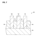
- first regions R 1 are selectively removed with respect to the second regions R 2 , as illustrated in FIG. 7 .
- the first regions R 1 are selectively etched back with respect to the second regions R 2 which are fin regions.
- a step of exposing a wafer W to plasma of a fluorocarbon-based gas is performed until it becomes necessary to selectively remove the first region R 1 with respect to the second region R 2 . That is, the plurality of sequences illustrated in FIG. 1 is performed after the step of exposing the wafer W to the plasma of the fluorocarbon-based gas.
- the fluorocarbon-based gas may include at least one of the above-described fluorocarbon gas and fluorohydrocarbon gas, and may further include another gas such as, for example, a rare gas.
- the plasma may be generated by any plasma source.
- the plasma may be generated using microwaves, may be generated by a capacitive coupling type plasma source, or may be generated by an inductive coupling type plasma source.
- a bias power for drawing ions in the plasma to the wafer W may be used.
- FIG. 8 is a view for describing a step of exposing a wafer W to a fluorocarbon-based gas.
- plasma PL 3 of the fluorocarbon-based gas is generated in the processing container in the step of exposing the wafer W to the plasma PL 3 of the fluorocarbon-based gas.
- the first region R 1 is etched.
- the step of exposing the wafer W to the plasma of the fluorocarbon-based gas may be performed until the head portions of the second regions R 2 are exposed or immediately before the head portions of the second regions R 2 are exposed, as illustrated in FIG. 8 .
- the first region R 1 may be removed at a high speed.
- the plurality of sequences illustrated in FIG. 1 is performed thereafter, the first region R 1 may be selectively removed with respect to the second regions R 2 .
- FIG. 9 illustrates an exemplary wafer state just after the step of exposing the wafer W to plasma of a fluorocarbon-based gas.
- the step of exposing the wafer W to plasma of the fluorocarbon-based gas may be performed until the first region R 1 partially remains along the side walls of the second regions R 2 as illustrated in FIG. 9 . Thereafter, the plurality of sequences illustrated in FIG. 1 may be performed in order to remove the first region R 1 remaining along the side walls.
- FIG. 10 is a flowchart illustrating still another exemplary embodiment of the method of selectively removing a region formed of silicon oxide.
- the method MT 2 illustrated in FIG. 10 includes step STa of exposing a wafer W to plasma of a fluorocarbon-based gas, and steps ST 2 and ST 4 described above.
- step STa of the method MT 2 the plasma PL 3 of the fluorocarbon-based gas is generated in the processing container as described above with reference to FIG. 8 .
- the first region R 1 is etched. That is, in step STa, the first region R 1 is etched back by the plasma PL 3 of the fluorocarbon-based gas.
- the height in the thickness direction of the first region R 1 partially increases at the areas along the side walls of the second regions R 2 as illustrated in FIG. 11 . That is, the first region R 1 takes a long tail shape from each of the side walls of the second regions R 2 .
- step ST 2 is performed in the method MT 2 . That is, in step ST 2 , as illustrated in FIG. 12 , plasma PL 1 of a processing gas containing hydrogen, nitrogen, and fluorine is generated within the processing container that accommodates the wafer W, and the wafer W is exposed to the plasma PL 1 . As a result, some regions including a portion of the first region R 1 , i.e., the surface of the first region R 1 is denatured.
- step ST 4 is performed in the method MT 2 . That is, in step ST 4 , the denatured region produced in step ST 2 is removed. By step ST 4 , the surface of the first region R 1 becomes relatively flat surface as illustrated in FIG. 13 . As described above, in step ST 4 , the denatured region produced in step ST 2 may be removed by heating the wafer W within the processing container. Alternatively, in step ST 4 , the plasma of the rare gas may be generated within the processing container and the wafer W may be exposed to the plasma so as to remove the denatured region. In addition, step ST 4 may be performed in a non-bias state.
- the surface of the first region R 1 etched back in step STa may be processed to a relatively flat surface by performing step ST 2 and step ST 4 following step STa.
- a series of steps including steps STa, ST 2 , and ST 4 may be performed within a single processing container, i.e., using a single plasma processing apparatus.
- step ST 3 may be performed between steps ST 2 and ST 4 .
- the plasma may be generated by any plasma source. For example, when the plasma is excited by microwaves, the first region R 1 between adjacent fins may be etched back by step STa without following a pitch between multiple fins which correspond to the second regions R 2 .
- FIG. 14 is a cross-sectional view schematically illustrating a plasma processing apparatus.
- the plasma processing apparatus 10 illustrated in FIG. 14 is provided with a processing container 12 .
- the processing container 12 defines a processing space S configured to accommodate a wafer W.
- the processing container 12 may include a side wall 12 a , a bottom 12 b , and a ceiling 12 c.
- the side wall 12 a has a substantially cylindrical shape centering substantially around an axis Z and extending in a direction in which the axis Z extends (hereinafter, referred to as an “axis Z direction”).
- the inner diameter of the side wall 12 a is, for example, 540 mm.
- the bottom 12 b is formed at the lower end side of the side wall 12 a .
- the top end of the side wall 12 a is opened.
- the opening at the top end of the side wall 12 a is closed by a dielectric window 18 .
- the dielectric window 18 is sandwiched between the top end of the side wall 12 a and the ceiling 12 c .
- a sealing member SL 1 may be interposed between the dielectric window 18 and the top end of the side wall 12 a .
- the sealing member SL 1 is, for example, an O-ring and contributes to the sealing of the processing container 12 .
- the plasma processing apparatus 10 is further provided with a mounting table 20 .
- the mounting table 20 is installed within the processing container 12 and below the dielectric window 18 .
- the mounting table 20 includes a plate 22 and an electrostatic chuck 24 .
- the plate 22 is a substantially disc-shaped metallic member and is formed of, for example, aluminum.
- the plate 22 is supported by a cylindrical support SP 1 .
- the support SP 1 extends vertically upward from the bottom 12 b .
- the plate 22 also serves as a high frequency electrode.
- the plate 22 is electrically connected to a high frequency power source RFG configured to generate a high frequency bias power, through a matching unit MU and a power feeding rod PFR.
- the high frequency power source RFG outputs a high frequency bias power having a predetermined frequency suitable for controlling energy of ions drawn into the wafer W, for example, 13.65 MHz.
- the matching unit MU accommodates a matcher configured to match impedance between the high frequency power source RFG side impedance and a load (mainly, such as, for example, an electrode, plasma, and the processing container 12 ) side impedance.
- a blocking condenser for self-bias generation is included within the matching unit.
- the electrostatic chuck 24 is installed on the top surface of the plate 22 .
- the electrostatic chuck 24 includes a base plate 24 a and a chuck portion 24 b .
- the base plate 24 a is a substantially disc-shaped metallic member, and is formed of, for example, aluminum.
- the base plate 24 a is installed on the plate 22 .
- the chuck portion 24 b is installed on the top surface of the base plate 24 a .
- the top surface of the chuck portion 24 b becomes a mounting region MR configured to mount a wafer W thereon.
- the chuck portion 24 b holds the wafer W with an electrostatic attractive force.
- the chuck portion 24 b includes an electrode film sandwiched between dielectric films.
- a direct current power source DSC is electrically connected to the electrode film of the chuck portion 24 b through a switch SW and a coated wire CL.
- the chuck portion 24 b may attract and hold the wafer W on the top surface thereof by a coulomb force generated by a direct voltage applied to the direct current power source DSC.
- a focus ring FR is provided radially outside of the chuck portion 24 b to annularly surround an edge of the wafer W.
- the plasma processing apparatus 10 is provided with a temperature control mechanism.
- An annular coolant chamber 24 g extending in a circumferential direction is installed inside the base plate 24 a as a portion of the temperature control mechanism.
- a coolant of a predetermined temperature for example, cooling water is circulated and supplied to the coolant chamber 24 g from a chiller unit through pipes PP 1 , PP 3 .
- the processing temperature of the wafer W on the chuck portion 24 b may be controlled depending on the temperature of the coolant.
- a heat transfer gas from a heat transfer gas supply unit for example, He gas is supplied to a gap between the top surface of the chuck portion 24 b and the rear surface of the wafer W through a gas supply tube PP 2 .
- the plasma processing apparatus 10 may be further provided with heaters HT, HS, HC, and HE as a portion of the temperature control mechanism.
- the heater HT is installed within the ceiling 12 c , and extends annularly to surround the antenna 14 .
- the heater HS is installed within the side wall 12 a and extends annularly.
- the heater HC is installed within the base plate 24 a .
- the heater HC is installed below a central portion of the above-described mounting region MR within the base plate 24 a , i.e., in a region intersecting the axis Z.
- the heater HE is installed within the base plate 24 a and extends annularly to surround the heater HC.
- the heater HE is installed below an outer peripheral portion of the above-described mounting region MR.
- annular exhaust passage VL is formed around the mounting table 20 .
- An annular baffle plate 26 formed with a plurality of through holes is installed in the middle of the exhaust passage VL in the axis Z direction.
- the exhaust passage VL is connected to an exhaust tube 28 that provides an exhaust port 28 h .
- the exhaust tube 28 is attached to the bottom 12 b of the processing container 12 .
- An exhaust apparatus 30 is connected to the exhaust tube 28 .
- the exhaust apparatus 30 includes a pressure regulator and a vacuum pump, for example, a turbo molecular pump.
- the processing space S within the processing container 12 may be decompressed to a desired vacuum degree by the exhaust apparatus 30 .
- gas may be exhausted from the outer circumference of the mounting table 20 through the exhaust passage VL.
- the plasma processing apparatus 10 is further provided with a plasma generation unit PG of an exemplary embodiment.
- the plasma generation unit PG includes an antenna 14 , a coaxial waveguide 16 , a dielectric window 18 , a microwave generator 32 , a tuner 34 , a waveguide 36 , and a mode converter 38 .
- the microwave generator 32 generates microwaves of, for example, a 2.45 GHz frequency.
- the microwave generator 32 is connected to an upper portion of a coaxial waveguide 16 through the tuner 34 , the waveguide 36 , and the mode converter 38 .
- the coaxial waveguide 16 extends along the axis Z which is the central axis thereof. In an exemplary embodiment, the center of the mounting region MR of the mounting table 20 is positioned on the axis Z.
- the coaxial waveguide 16 includes an outer conductor 16 a and an inner conductor 16 b .
- the outer conductor 16 a has a cylindrical shape extending along the axis Z which is the central axis thereof.
- the lower end of the outer conductor 16 a may be electrically connected to an upper portion of a cooling jacket 40 having a conductive surface.
- the inner conductor 16 b is installed inside the outer conductor 16 a coaxially to the outer conductor 16 a .
- the inner conductor 16 b has a cylindrical shape extending along the axis Z which is the central axis thereof.
- the lower end of the inner conductor 16 b is connected to the slot plate 44 of the antenna 14 .
- the antenna 14 is a radial line slot antenna.
- the antenna 14 is placed inside the opening formed in the ceiling 12 c , and installed on the top surface of the dielectric window 18 .
- the antenna 14 includes a dielectric plate 42 and a slot plate 44 .
- the dielectric plate 42 shortens the wavelength of microwaves and has substantially a disc shape.
- the dielectric plate 42 is formed of, for example, quartz or alumina.
- the dielectric plate 42 is sandwiched between the slot plate 44 and a lower surface of the cooling jacket 40 . Accordingly, the antenna 14 may be configured by the dielectric plate 42 , the slot plate 44 , and the cooling jacket 40 .
- FIG. 15 is a plan view illustrating an exemplary slot plate.
- the slot plate 44 is a thin plate type and is disc-shaped. The both sides of the slot plate 44 in the thickness direction are parallel to each other.
- the center CS of the circular slot plate 44 is positioned on the axis Z.
- a plurality of slot pairs 44 p is provided in the slot plate 44 .
- Each of the plurality of slot pairs 44 p includes two slot holes 44 a , 44 b penetrating the slot plate 44 in the thickness direction.
- the planar shape of each of the slot holes 44 a , 44 b has an elongated hole shape. In each slot pair 44 p , a major axis direction of the slot hole 44 a and a major axis direction of the slot hole 44 b intersect or are orthogonal to each other.
- the plurality of slot pairs 44 p is classified into an inner slot pair group ISP provided inside a virtual circle VC around the axis Z and an outer slot pair group OSP provided outside the virtual circle VC.
- the inner slot pair group ISP includes a plurality of slot pairs 44 p .
- the inner slot pair group ISP includes seven (7) slot pairs 44 p .
- the plurality of slot pairs 44 p of the inner slot pair group ISP is arranged at regular intervals in a circumferential direction with respect to the center CS.
- the plurality of slot holes 44 a included in the inner slot pair group ISP is arranged at regular intervals such that the centers of gravity of the slot holes 44 a are positioned on a circle having a radius r1 from the center CS of the slot plate 44 .
- the plurality of slot holes 44 b included in the inner slot pair group ISP is arranged at regular intervals such that the centers of gravity of the slot holes 44 b are positioned on a circle having a radius r2 from the center CS of the slot plate 44 .
- the radius r2 is larger than the radius r1.
- the outer slot pair group OSP includes a plurality of slot pairs 44 p .
- the outer slot pair group OSP includes twenty eight (28) slot pairs 44 p .
- the plurality of slot pairs 44 p of the outer slot pair group OSP is arranged at regular intervals in the circumferential direction with respect to the center CS.
- the plurality of slot holes 44 a included in the outer slot pair group OSP is arranged at regular intervals such that the centers of gravity of the slot holes 44 a are positioned on a circle having a radius r3 from the center CS of the slot plate 44 .
- the plurality of slot holes 44 b included in the outer slot pair group OSP are arranged at regular intervals such that the centers of gravity of slot holes 44 b is positioned on a circle having a radius r4 from the center CS of the slot plate 44 .
- the radius r3 is larger than the radius r2 and the radius r4 is larger than the radius r3.
- respective slot holes 44 a of the inner slot pair group ISP and the outer slot pair group OSP are formed such that the major axes thereof have the same angle with respect to segments connecting the center CS and the centers of gravity thereof.
- slot holes 44 b of the inner slot pair group ISP and the outer slot pair group OSP are formed such that the major axes thereof have the same angle with respect to segments connecting the center CS and the centers of gravity thereof.
- FIG. 16 is a plan view illustrating an exemplary dielectric window in which a state of the dielectric window viewed from the processing space S side is illustrated.
- FIG. 17 is a cross-sectional view taken along line XVII-XVII of FIG. 16 .
- the dielectric window 18 has substantially a disc shape and formed of a dielectric material such as, for example, quartz or alumina.
- the slot plate 44 is installed on the upper surface 18 u of the dielectric window 18 .
- a through hole 18 h is formed at a central portion of the dielectric window 18 .
- An upper portion of the through hole 18 h provides a space 18 s to accommodate an injector 50 b of a central introduction unit 50 , and a lower portion is a central introduction port 18 i of the central introduction unit 50 .
- the central introduction unit 50 will be described below.
- the central axis of the dielectric window 18 coincides with the axis Z.
- the lower surface 18 b defines various shapes. Specifically, the lower surface 18 b includes a flat surface 180 in a central region surrounding the central introduction port 18 i .
- the flat surface 180 is a flat surface orthogonal to the axis Z.
- the lower surface 18 b is annually continued in a region radially outside the flat surface 180 to define a first annular concave portion 181 recessed in a tapered shape toward the inside of the dielectric window 18 in the plate thickness direction.
- the first concave portion 181 is defined by an inner tapered surface 181 a , a bottom surface 181 b , and an outer tapered surface 181 c .
- the bottom surface 181 b is formed closer to the upper surface 18 u side than the flat surface 180 and extends annularly to be parallel to the flat surface 180 .
- the inner tapered surface 181 a extends annularly between the flat surface 180 and the bottom surface 181 b and is inclined in relation to the flat surface 180 .
- the outer tapered surface 181 c extends annularly between the bottom surface 181 b and the peripheral edge of the lower surface 18 b and is inclined in relation to the bottom surface 181 b . Meanwhile, the peripheral edge region of the lower surface 18 b becomes a surface which is in contact with the side wall 12 a.
- the lower surface 18 b defines a plurality of second concave portions 182 which is recessed from the flat surface 180 toward the inside of the dielectric window 18 in the plate thickness direction.
- the number of the second concave portions 182 is seven in the example illustrated in FIGS. 16 and 17 .
- the plurality of second concave portions 182 is formed at regular intervals along the circumferential direction.
- the plurality of second concave portions 182 has a circular plane shape in a plane orthogonal to the axis Z.
- the inner surface 182 a defining the second concave portions 182 is a cylindrical surface extending in the axis Z direction.
- the bottom surface 182 b defining the second concave portions 182 is formed closer to the upper surface 18 u side than the flat surface 180 and is a circular surface parallel to the flat surface 180 .
- FIG. 18 is a bottom plan view illustrating a state where the slot plate illustrated in FIG. 15 is placed above the dielectric window illustrated in FIG. 16 in which the dielectric window 18 is viewed from the bottom side.
- the plurality of slot holes 44 a and the plurality of slot holes 44 b of the outer slot pair group OSP and the plurality of slot holes 44 b of the inner slot pair group ISP overlap with the first concave portion 181 .
- the plurality of slot holes 44 b of the outer slot pair group OSP partially overlaps with outer tapered surface 181 c and partially overlaps the bottom surface 181 b .
- the plurality of slot holes 44 a of the outer slot pair group OSP overlaps with the bottom surface 181 b .
- the plurality of slot holes 44 b of the inner slot pair group ISP partially overlaps with the inner tapered surface 181 a and partially overlaps with the bottom surface 181 b.
- the plurality of slot holes 44 a of the inner slot pair group ISP overlaps with the second concave portions 182 .
- each of centers of gravity (center) of the bottom surfaces of the plurality of second concave portions 182 are positioned within the plurality of slot holes 44 a of the inner slot pair group ISP, respectively.
- microwaves generated by the microwave generator 32 are propagated to the dielectric plate 42 through the coaxial waveguide 16 and provided to the dielectric window 18 from the slot holes 44 a and 44 b of the slot plate 44 .
- the plate thickness of the portion defining the first concave portion 181 and the plate thickness of the portion defining the second concave portions 182 are thinner than the other portion. Accordingly, in the dielectric window 18 , the microwave transmissibility becomes higher at the portion defining the first concave portion 181 and the portion defining the second concave portions 182 .
- the slot holes 44 a and 44 b of the outer slot pair group OSP and the slot holes 44 b of the inner slot pair group ISP overlap with the first concave portion 181
- the slot holes 44 a of the inner slot pair group ISP overlap with the second concave portion 182 .
- the plasma processing apparatus 10 further include a central introduction unit 50 and a peripheral introduction unit 52 .
- the central introduction unit 50 includes a duct 50 a , an injector 50 b , and a central introduction port 18 i .
- the duct 50 a is configured to pass through a bore inside the inner conductor 16 b of the coaxial waveguide 16 .
- an end of the duct 50 a extends to the inside of the space 18 s (see, for example, FIG. 17 ) defined along the axis Z by the dielectric window 18 .
- the injector 50 b is accommodated inside the space 18 s and below the end of the duct 50 a .
- the injector 50 b a plurality of through holes is formed to extend in the axis Z direction. Further, the dielectric window 18 defines the central introduction port 18 i . The central introduction port 18 i is continued downward from the space 18 s and extends along the axis Z.
- the central introduction unit 50 with this configuration supplies a gas to the injector 50 b through the duct 50 a so that the gas is injected from the injector 50 b through the central introduction port 18 i . In this manner, the central introduction unit 50 injects the gas to an area just below the dielectric window 18 along the axis Z. That is, the central introduction unit 50 introduces the gas into a plasma generation region with a high electron temperature.
- the peripheral introduction unit 52 includes a plurality of peripheral introduction ports 52 i .
- the plurality of peripheral introduction ports 52 i mainly provides the gas to an edge region of a wafer W.
- the plurality of peripheral introduction ports 52 i are opened toward the edge region of the wafer W or an edge of a mounting region MR.
- the plurality of peripheral introduction ports 52 i is arranged along a circumferential direction below the central introduction port 18 i and above the mounting table 20 . That is, the plurality of peripheral introduction ports 52 i are arranged annularly around the axis Z in a region (plasma diffusion region) having a lower electron temperature than a position just below the dielectric window.
- the peripheral introduction unit 52 supplies the gas to the wafer in the region having a low electron temperature. Accordingly, a degree of dissociation of the gas introduced into the processing space S from the peripheral introduction unit 52 is more suppressed than a degree of dissociation of the gas supplied to the processing space S from the central introduction unit 50 .
- a first gas source group GSG 1 is connected to the central introduction unit 50 through a first flow control unit group FCG 1 .
- a second gas source group GSG 2 is connected to the peripheral introduction unit 52 through a second flow control unit group FCG 2 .
- FIG. 19 is a view illustrating a gas supply unit including the first flow control unit group, the first gas source group, the second flow control unit group, and the second gas source group. As illustrated in FIG. 19 , the first gas source group GSG 1 , the first flow control unit group FCG 1 , the second gas source group GSG 2 , and the second flow control unit group FCG 2 constitute a gas supply unit GU of an exemplary embodiment.
- the first gas source group GSG 1 includes a plurality of first gas sources GS 11 to GS 15 .
- the gas source GS 11 is a source of a hydrogen containing gas, for example of a source of H2 gas.
- the gas source GS 12 is a source of a nitrogen containing gas, for example, a source of N2 gas.
- the gas source GS 13 is a source of a fluorine containing gas.
- the fluorine containing gas one or more gases selected from the above-described fluorocarbon gas, fluorohydrocarbon gas, NF3 gas, and SF6 gas may be used.
- the gas source GS 14 is a source of a rare gas, for example, a source of Ar gas.
- the gas source GS 15 is a source of the above-described fluorocarbon-based gas.
- the first flow control unit group FCG 1 includes a plurality of first flow control units FC 11 to FC 15 .
- Each of the plurality of first flow control units FC 11 to FC 15 includes, for example, two valves and a flow controller provided between the two valves.
- the flow controller is, for example, a mass flow controller.
- the plurality of first gas sources GS 11 to GS 15 is connected to a common gas line GL 1 through the plurality of first flow control units FC 11 to FC 15 , respectively.
- the common gas line GL 1 is connected to the central introduction unit 50 .
- the second gas source group GSG 2 includes a plurality of first gas sources GS 21 to GS 25 .
- the second gas sources GS 21 to GS 25 are gas sources which are similar to the gas sources GS 11 to GS 15 , respectively.
- the second flow control unit group FCG 2 includes a plurality of second flow control units FC 21 to FC 25 .
- Each of the plurality of second flow control units FC 21 to FC 25 includes, for example, two valves, and a flow controller installed between the two valves.
- the flow controller is, for example, a mass flow controller.
- the plurality of second gas sources GS 21 to GS 25 is connected to a common gas line GL 2 through the plurality of second flow control units FC 21 to FC 25 , respectively.
- the common gas line GL 2 is connected to the peripheral introduction unit 52 .
- the plurality of first gas sources and the plurality of first flow control units are provided to be exclusively used by the central introduction unit 50
- the plurality of second gas sources and the plurality of second flow control units which are independent from the plurality of first gas sources and the plurality of first flow control units are provide to be exclusively used by the peripheral introduction unit 52 .
- the kind of gas introduced into the processing space S from the central introduction unit 50 and a flow rate of one or more gases introduced into the processing space S from the central introduction unit 50 may be independently controlled.
- the kind of gas introduced into the processing space S from the peripheral introduction unit 52 , and a flow rate of one or more gases introduced into the processing space S from peripheral introduction unit 52 may be independently controlled.
- the peripheral introduction unit 52 further includes an annular tube 52 p .
- the annular tube 52 p is formed with a plurality of peripheral introduction ports 52 i .
- the annular tube 52 p may be formed of, for example, quartz.
- the annular tube 52 p is installed along the inner wall surface of the side wall 12 a .
- the annular tube 52 p is not disposed on the lower surface of the dielectric window 18 and in the mounting region MR, that is, on a route connecting a wafer W. Accordingly, the annular tube 52 p does not impede the diffusion of plasma.
- annular tube 52 p is installed along the inner wall surface of the side wall 12 a , consumption of the annular tube 52 p by plasma may be suppressed, and thus, exchange frequency of the annular tube 52 p may be reduced. Further, since the annular tube 52 p is installed along the side wall 12 which may be subjected to a temperature control by a heater, the temperature stability of a gas introduced into the processing space S from the peripheral introduction unit 52 may be enhanced.
- the plurality of peripheral introduction ports 52 i is opened toward the edge region of the wafer W. That is, the plurality of peripheral introduction ports 52 i is inclined in relation to a plane orthogonal to the axis Z so as to inject a gas toward the edge region of the wafer W. Since the peripheral introduction ports 52 i are opened to be inclined toward the edge region of the wafer W as described above, an active species of the gas injected from the peripheral introduction ports 52 i is directly headed for the edge region of the wafer W. As a result, the active species of the gas may be directly supplied to the edge of the wafer W without being deactivated.
- the plasma processing apparatus 10 further includes a control unit Cnt.
- the control unit Cnt may be a programmable controller such as, for example, a computer device.
- the control unit Cnt may control each unit of the plasma processing apparatus 10 according to a program based on a recipe.
- step ST 1 of the method MT illustrated in FIG. 1 the control unit Cnt executes a control of causing the gas supply unit GU to supply a reducing gas and the plasma generation unit PG to generate energy.
- the gas supply unit GU supplies a mixed gas of the gases from the gas sources GS 11 , GS 12 , GS 21 , GS 22 into the processing container 12 as a reducing gas.
- the plasma generation unit PG introduces microwaves into the processing container 12 through the dielectric window 18 . As a result, plasma of the reducing gas is generated and the wafer W is exposed to the plasma.
- the control unit Cnt may stop the supply of a high frequency bias power from the high frequency power source RFG to the plate 22 , that is, a high frequency electrode. That is, the control unit Cnt may perform step ST 1 in a non-bias manner. Meanwhile, in a control for performing step ST 1 , the control unit Cnt may cause the gas supply unit GU to supply a rare gas such as, for example, He gas, instead of the gases from the gas sources GS 12 , GS 22 .
- a rare gas such as, for example, He gas
- the control unit Cnt executes a control of causing the gas supply unit GU to supply a processing gas and the plasma generation unit PG to generate energy.
- the gas supply unit GU supplies a mixed gas of the gases from the gas sources GS 11 , GS 12 , GS 13 , GS 21 , GS 22 , GS 23 into the processing container 12 as a processing gas.
- the plasma generation unit PG introduces microwaves into the processing container 12 through the dielectric window 18 . As a result, plasma of the processing gas is generated and the wafer W is exposed to the plasma.
- the control unit Cnt may stop the supply of a high frequency bias power from the high frequency power source RFG to the plate 22 , i.e., a high frequency electrode.
- the control unit Cnt executes a control of causing the gas supply unit GU to supply a rare gas and the plasma generation unit PG to generate energy, and operating the exhaust apparatus 30 .
- the gas supply unit GU supplies the rare gas from the gas sources GS 14 , GS 24 into the processing container 12 .
- the plasma generation unit PG introduces microwaves into the processing container 12 through dielectric window 18 . As a result, plasma of the rare gas is generated, and the processing space S within the processing container 12 is exhausted such that the inside of the processing container 12 is cleaned.
- control unit Cnt when performing step ST 4 of the method MT and the method MT 2 , the control unit Cnt performs a control of causing the heaters HC and HE to generate heat.
- the control unit Cnt may control the gas supply unit GU to supply the rare gas from the gas sources GS 14 , GS 24 into the processing container 12 .
- the control unit Cnt performs a control of causing the gas supply unit GU to supply a rare gas and the plasma generation unit PG to generate energy.
- the gas supply unit GU supplies the rare gas from the gas sources GS 14 , GS 24 into the processing container 12 .
- the plasma generation unit PG introduces microwaves into the processing container 12 through the dielectric window 18 . As a result, plasma of the rare gas is generated, and the wafer W is exposed to the plasma.
- the control unit Cnt may stop the supply of a high frequency bias power from the high frequency power source RFG to the plate 22 , that is, a high frequency electrode.
- the control unit Cnt executes a control of causing the gas supply unit GU to supply the fluorocarbon-based gas and the plasma generation unit PG to generate energy.
- the gas supply unit GU supplies the fluorocarbon-based gas from the gas sources GS 15 , GS 25 into the processing container 12 .
- the plasma generation unit PG introduces microwaves into the processing container 12 through the dielectric window 18 .
- control unit Cnt may cause the gas supply unit GU to supply, for example, a rare gas, into the processing container in addition to the fluorocarbon-based gas.
- control unit Cnt may cause the high frequency power source RFG to supply a high frequency bias power to the plate 22 .
- Test Example 1 a sequence processing including step ST 2 and step ST 4 was performed once on wafers having a silicon oxide film.
- the pressure within the processing container 12 when performing step ST 2 was variously set as a variable parameter.
- the other processing conditions of Test Example 1 were as follows.
- Wafer temperature 30° C.
- Wafer temperature 120° C.
- Test Example 1 a changed amount in film thickness of silicon oxide films before and after the processing, i.e., an etching amount was measured.
- the result is represented in FIG. 20 .
- the horizontal axis represents a pressure within the processing container 12 when performing step ST 2
- the vertical axis represents an etching amount.
- a relatively large etching amount may be obtained when the pressure within the processing container 12 at the time of performing step ST 2 is in a range of 40 Pa (300 mTorr) to 66.66 Pa (500 mTorr).
- Test Example 2 a sequence processing including steps ST 2 and ST 4 was performed twice on wafers having a region where a first region formed of silicon oxide and a second region formed of silicon were densely formed (hereinafter, referred to as a “dense region”) and a region where the first region and the second region were coarsely formed (hereinafter, referred to as a “coarse region”).
- the microwave power at the time of performing step ST 2 was variously set as a variable parameter.
- the other processing conditions of Test Example 2 were as follows.
- Wafer temperature 50° C.
- Wafer temperature 80° C.
- Test Example 2 a changed amount in film thickness of silicon oxide films before and after the processing, i.e., an etching amount was measured at each of the coarse region and the dense region.
- the result is represented in FIG. 21 .
- the horizontal axis in FIG. 21 represents a microwave power when performing step ST 2
- the vertical axis represents an etching amount.
- FIG. 21 as a result of Test Example 2, it was found that the difference in etching amount between the coarse region and the dense region is reduced when the microwave power at the time of performing step ST 2 is in a range of 2000 W to 3000 W.
- Test Example 3 i.e., Test Example 3-1, Test Example 3-2, and Test Example 33
- a sequence processing including step ST 2 and step ST 4 was performed once to three times on wafers having a silicon oxide film.
- the flow rate of N 2 gas at the time of performing step ST 2 was variously set as a variable parameter. Specifically, in Test Example 3-1, the flow rate of N 2 gas in step ST 2 was set to 300 sccm, and the sequence processing was performed three times.
- the flow rate of N 2 gas in step ST 2 was set to 500 sccm, and the sequence processing was performed once.
- the flow rate of N 2 gas in step ST 2 was set to 1000 sccm and the sequence processing was performed once.
- the other processing conditions were as follows.
- Wafer temperature 15° C.
- Wafer temperature 50° C.
- Wafer temperature 30° C.
- Wafer temperature 30° C.
- Wafer temperature 30° C.
- Wafer temperature 30° C.
- a changed amount in film thickness of the silicon oxide films before and after the processing that is, an etching amount was measured.
- the result (an etching amount per one sequence) is represented in FIG. 22 .
- the horizontal axis represents a flow rate of N 2 gas when step ST 2 is performed, and the vertical axis represents an etching amount.
- the flow rate of N 2 gas at the time of performing step ST 2 is in a range of 300 sccm to 1000 sccm.
- Test Example 4 a sequence processing including step ST 2 and step ST 4 is performed once on wafers having a silicon oxide film.
- the flow rate of SF 6 gas at the time of performing step ST 2 was variously set as a variable parameter.
- the other processing conditions in Test Example 4 were as follows.
- Wafer temperature 30° C.
- Wafer temperature 120° C.
- Test Example 4 a changed amount in film thickness of silicon oxide films before and after the processing, that is, an etching amount.
- the result is represented in FIG. 23 .
- the horizontal axis in FIG. 23 represents a flow rate of SF 6 gas at the time of performing step ST 2 and the vertical axis represents an etching amount.
- a relatively large etching amount may be obtained when a ratio occupied by the flow rate of SF 6 gas in the entire flow rate of the processing gas at the time of performing step ST 2 is in a range of 3% to 8%.
- Test Example 5 a sequence processing including step ST 2 and step ST 4 was performed once on wafers having a silicon oxide film.
- the wafer temperature at the time of performing step ST 2 was variously set as a variable parameter.
- the other processing conditions in Test Example 5 were as follows.
- Wafer temperature 30° C.
- Test Example 5 a changed amount in film thickness of silicon oxide films before and after the processing, i.e., an etching amount.
- the result is represented in FIG. 24 .
- the horizontal axis in FIG. 24 represents a wafer temperature and the vertical axis represents an etching amount.
- a relatively large etching amount may be obtained when the wafer temperature at the time of performing step ST 2 is in a range of 20° C. to 40° C.
- Test Example 6 a sequence including step ST 2 and step ST 4 was performed once on wafers having a silicon oxide film.
- a sequence including step ST 2 and step ST 4 was performed once on wafers having a polysilicon film.
- Test Example 8 a sequence including step ST 2 and step ST 4 was performed twice on wafers having a silicon oxide film.
- Test Example 9 a sequence including step ST 2 and step ST 4 was performed twice on wafers having a polysilicon film. Meanwhile, in Test Examples 8 and 9, step ST 1 was not performed in the second sequence.
- Test Example 10 a sequence including step ST 2 and step ST 4 was performed twice on wafers having a silicon oxide film and step ST 1 was performed in the second sequence.
- step ST 2 was performed twice on wafers having a polysilicon film and step ST 1 was performed in the second sequence and step ST 1 was performed in the second sequence.
- the conditions in step ST 1 , step ST 2 , and step ST 4 were as follows.
- Wafer temperature 50° C.
- Wafer temperature 50° C.
- Wafer temperature 80° C.
- Test Examples 6 to 11 a changed amount in film thickness of silicon oxide films before and after the processing, i.e., an etching amount was measured on each of four diameters passing through the centers of wafers at 45 degree intervals, that is, an X-axis, a Y-axis, a V-axis, and a W-axis.
- the etching amounts obtained in Test Examples 6 and 7 are represented in FIGS. 25A and 25B , respectively
- the etching amounts obtained in Test Examples 8 and 9 are represented in FIGS. 26A and 26B , respectively
- the etching amounts obtained in Test Examples 10 and 11 are represented in FIGS. 27A and 27B , respectively.
- each horizontal axis represents a position from a wafer center, and each vertical axis represents an etching amount.
- each silicon oxide film was etched, as represented in FIG. 25A , and each polysilicon film was not substantially etched, as illustrated in FIG. 25B .
- the silicon oxide film was etched in an etching amount larger than that in the first sequence as represented in FIGS. 26A and 27A .
- step ST 1 since step ST 1 was not performed in the second sequence, polysilicon films were also etched, as represented in FIG. 26B .
- the etching amounts of polysilicon films were reduced as compared those in Test Example 9, as represented in FIG. 27B .
- Test Examples 12 and 13 a sequence including step ST 2 and step ST 4 was performed once on wafers including a silicon oxide film.
- the wafer temperature at the time of performing step ST 4 was set to 120° C.
- the wafer temperature at the time of performing step ST 2 was set to 80° C.
- the other processing conditions in Test Examples 12 and 13 were as follows.
- step ST 4 In order to etching the silicon oxide films by the same amount in the thickness direction, in Test Example 12, the processing time of one minute is required for step ST 4 , and in Test Example 13, the processing time of 10 minutes was required for step ST 4 . That is, it was found that in step ST 4 in which a denatured region is removed, the processing time of step ST 4 may be reduced as the wafer temperature increased.
- an inductive coupling type plasma processing apparatus may be used without being limited to the plasma processing apparatus which uses microwaves as a plasma source.
Applications Claiming Priority (4)
| Application Number | Priority Date | Filing Date | Title |
|---|---|---|---|
| JP2013180267 | 2013-08-30 | ||
| JP2013-180267 | 2013-08-30 | ||
| JP2013256118A JP6086862B2 (ja) | 2013-08-30 | 2013-12-11 | 酸化シリコンから構成された領域を選択的に除去する方法及びプラズマ処理装置 |
| JP2013-256118 | 2013-12-11 |
Publications (2)
| Publication Number | Publication Date |
|---|---|
| US20150064922A1 US20150064922A1 (en) | 2015-03-05 |
| US9502537B2 true US9502537B2 (en) | 2016-11-22 |
Family
ID=52583837
Family Applications (1)
| Application Number | Title | Priority Date | Filing Date |
|---|---|---|---|
| US14/469,784 Active US9502537B2 (en) | 2013-08-30 | 2014-08-27 | Method of selectively removing a region formed of silicon oxide and plasma processing apparatus |
Country Status (3)
| Country | Link |
|---|---|
| US (1) | US9502537B2 (ja) |
| JP (1) | JP6086862B2 (ja) |
| KR (1) | KR101755077B1 (ja) |
Cited By (1)
| Publication number | Priority date | Publication date | Assignee | Title |
|---|---|---|---|---|
| US10340123B2 (en) * | 2016-05-26 | 2019-07-02 | Tokyo Electron Limited | Multi-frequency power modulation for etching high aspect ratio features |
Families Citing this family (5)
| Publication number | Priority date | Publication date | Assignee | Title |
|---|---|---|---|---|
| JP6086862B2 (ja) * | 2013-08-30 | 2017-03-01 | 東京エレクトロン株式会社 | 酸化シリコンから構成された領域を選択的に除去する方法及びプラズマ処理装置 |
| JP6438831B2 (ja) * | 2015-04-20 | 2018-12-19 | 東京エレクトロン株式会社 | 有機膜をエッチングする方法 |
| TWI711716B (zh) * | 2017-06-06 | 2020-12-01 | 美商應用材料股份有限公司 | 使用沉積-處理-蝕刻製程之矽的選擇性沉積 |
| US10770305B2 (en) * | 2018-05-11 | 2020-09-08 | Tokyo Electron Limited | Method of atomic layer etching of oxide |
| WO2024079776A1 (ja) * | 2022-10-11 | 2024-04-18 | 株式会社日立ハイテク | プラズマ処理方法 |
Citations (11)
| Publication number | Priority date | Publication date | Assignee | Title |
|---|---|---|---|---|
| US5306671A (en) * | 1990-07-09 | 1994-04-26 | Mitsubishi Denki Kabushiki Kaisha | Method of treating semiconductor substrate surface and method of manufacturing semiconductor device including such treating method |
| US5328558A (en) * | 1992-03-25 | 1994-07-12 | Tokyo Electron Limited | Method for etching an SiO2 film |
| US5863339A (en) * | 1995-12-15 | 1999-01-26 | Nec Corporation | Chamber etching of plasma processing apparatus |
| US6706334B1 (en) * | 1997-06-04 | 2004-03-16 | Tokyo Electron Limited | Processing method and apparatus for removing oxide film |
| WO2005062344A1 (en) | 2003-12-17 | 2005-07-07 | Tokyo Electron Limited | Method of operating a system for chemical oxide removal |
| US20070030380A1 (en) * | 2005-07-20 | 2007-02-08 | Toshihiro Higuchi | Solid-state image sensing device and method for fabricating the same |
| JP2008016869A (ja) | 1998-11-11 | 2008-01-24 | Tokyo Electron Ltd | 表面処理方法及びその装置 |
| WO2011025655A2 (en) | 2009-08-31 | 2011-03-03 | Applied Materials, Inc. | Silicon-selective dry etch for carbon-containing films |
| US20150064922A1 (en) * | 2013-08-30 | 2015-03-05 | Tokyo Electron Limited | Method of selectively removing a region formed of silicon oxide and plasma processing apparatus |
| US20150162203A1 (en) * | 2013-12-11 | 2015-06-11 | Tokyo Electron Limited | Method for etching silicon layer and plasma processing apparatus |
| US20160005651A1 (en) * | 2014-07-01 | 2016-01-07 | Tokyo Electron Limited | Workpiece processing method |
Family Cites Families (3)
| Publication number | Priority date | Publication date | Assignee | Title |
|---|---|---|---|---|
| JP4495471B2 (ja) * | 2004-01-13 | 2010-07-07 | 三星電子株式会社 | エッチング方法 |
| JP5229711B2 (ja) * | 2006-12-25 | 2013-07-03 | 国立大学法人名古屋大学 | パターン形成方法、および半導体装置の製造方法 |
| JP5248902B2 (ja) * | 2007-10-11 | 2013-07-31 | 東京エレクトロン株式会社 | 基板処理方法 |
-
2013
- 2013-12-11 JP JP2013256118A patent/JP6086862B2/ja active Active
-
2014
- 2014-08-27 US US14/469,784 patent/US9502537B2/en active Active
- 2014-08-29 KR KR1020140113923A patent/KR101755077B1/ko active Search and Examination
Patent Citations (14)
| Publication number | Priority date | Publication date | Assignee | Title |
|---|---|---|---|---|
| US5306671A (en) * | 1990-07-09 | 1994-04-26 | Mitsubishi Denki Kabushiki Kaisha | Method of treating semiconductor substrate surface and method of manufacturing semiconductor device including such treating method |
| US5328558A (en) * | 1992-03-25 | 1994-07-12 | Tokyo Electron Limited | Method for etching an SiO2 film |
| US5863339A (en) * | 1995-12-15 | 1999-01-26 | Nec Corporation | Chamber etching of plasma processing apparatus |
| US6706334B1 (en) * | 1997-06-04 | 2004-03-16 | Tokyo Electron Limited | Processing method and apparatus for removing oxide film |
| JP2008016869A (ja) | 1998-11-11 | 2008-01-24 | Tokyo Electron Ltd | 表面処理方法及びその装置 |
| JP2007515074A (ja) | 2003-12-17 | 2007-06-07 | 東京エレクトロン株式会社 | 化学的酸化物除去(ChemicalOxideRemoval)システムの操作方法 |
| WO2005062344A1 (en) | 2003-12-17 | 2005-07-07 | Tokyo Electron Limited | Method of operating a system for chemical oxide removal |
| US20070030380A1 (en) * | 2005-07-20 | 2007-02-08 | Toshihiro Higuchi | Solid-state image sensing device and method for fabricating the same |
| WO2011025655A2 (en) | 2009-08-31 | 2011-03-03 | Applied Materials, Inc. | Silicon-selective dry etch for carbon-containing films |
| JP2013503482A (ja) | 2009-08-31 | 2013-01-31 | アプライド マテリアルズ インコーポレイテッド | 炭素含有膜のシリコン選択的ドライエッチング |
| US20150064922A1 (en) * | 2013-08-30 | 2015-03-05 | Tokyo Electron Limited | Method of selectively removing a region formed of silicon oxide and plasma processing apparatus |
| US20150162203A1 (en) * | 2013-12-11 | 2015-06-11 | Tokyo Electron Limited | Method for etching silicon layer and plasma processing apparatus |
| US20160005651A1 (en) * | 2014-07-01 | 2016-01-07 | Tokyo Electron Limited | Workpiece processing method |
| US9330973B2 (en) * | 2014-07-01 | 2016-05-03 | Tokyo Electron Limited | Workpiece processing method |
Cited By (1)
| Publication number | Priority date | Publication date | Assignee | Title |
|---|---|---|---|---|
| US10340123B2 (en) * | 2016-05-26 | 2019-07-02 | Tokyo Electron Limited | Multi-frequency power modulation for etching high aspect ratio features |
Also Published As
| Publication number | Publication date |
|---|---|
| JP2015065393A (ja) | 2015-04-09 |
| US20150064922A1 (en) | 2015-03-05 |
| KR20150026962A (ko) | 2015-03-11 |
| JP6086862B2 (ja) | 2017-03-01 |
| KR101755077B1 (ko) | 2017-07-19 |
Similar Documents
| Publication | Publication Date | Title |
|---|---|---|
| JP6498022B2 (ja) | エッチング処理方法 | |
| US9502537B2 (en) | Method of selectively removing a region formed of silicon oxide and plasma processing apparatus | |
| US9236265B2 (en) | Silicon germanium processing | |
| US9087798B2 (en) | Etching method | |
| US10121674B2 (en) | Method for etching silicon layer and plasma processing apparatus | |
| KR102099408B1 (ko) | 플라즈마 에칭 방법 및 플라즈마 에칭 장치 | |
| KR102114922B1 (ko) | 플라즈마 처리 방법 | |
| US9818582B2 (en) | Plasma processing method | |
| US9105585B2 (en) | Etching method | |
| KR20190008227A (ko) | 에칭 방법 | |
| KR20160134537A (ko) | 에칭 방법 | |
| US9412607B2 (en) | Plasma etching method | |
| US9034698B2 (en) | Semiconductor device manufacturing method | |
| US20190259578A1 (en) | Cleaning method and plasma processing apparatus | |
| US9305795B2 (en) | Plasma processing method | |
| CN111326395A (zh) | 等离子体处理方法和等离子体处理装置 | |
| US20150294839A1 (en) | Plasma processing apparatus and plasma processing method | |
| CN113206016A (zh) | 氧化物半导体膜的蚀刻方法和等离子体处理装置 |
Legal Events
| Date | Code | Title | Description |
|---|---|---|---|
| AS | Assignment |
Owner name: TOKYO ELECTRON LIMITED, JAPAN Free format text: ASSIGNMENT OF ASSIGNORS INTEREST;ASSIGNORS:KITAMURA, AKINORI;OHTAKE, HIROTO;SUZUKI, EIJI;SIGNING DATES FROM 20140826 TO 20140828;REEL/FRAME:033741/0529 |
|
| STCF | Information on status: patent grant |
Free format text: PATENTED CASE |
|
| MAFP | Maintenance fee payment |
Free format text: PAYMENT OF MAINTENANCE FEE, 4TH YEAR, LARGE ENTITY (ORIGINAL EVENT CODE: M1551); ENTITY STATUS OF PATENT OWNER: LARGE ENTITY Year of fee payment: 4 |