US9501079B2 - Data retention voltage clamp - Google Patents
Data retention voltage clamp Download PDFInfo
- Publication number
- US9501079B2 US9501079B2 US14/069,417 US201314069417A US9501079B2 US 9501079 B2 US9501079 B2 US 9501079B2 US 201314069417 A US201314069417 A US 201314069417A US 9501079 B2 US9501079 B2 US 9501079B2
- Authority
- US
- United States
- Prior art keywords
- circuit
- line
- voltage
- input signal
- transistor
- Prior art date
- Legal status (The legal status is an assumption and is not a legal conclusion. Google has not performed a legal analysis and makes no representation as to the accuracy of the status listed.)
- Expired - Fee Related
Links
- 230000014759 maintenance of location Effects 0.000 title claims description 15
- 238000000034 method Methods 0.000 claims description 43
- 230000015654 memory Effects 0.000 claims description 40
- 230000008859 change Effects 0.000 claims description 39
- 230000008569 process Effects 0.000 claims description 25
- 230000007423 decrease Effects 0.000 claims description 7
- 230000036039 immunity Effects 0.000 claims description 7
- 238000004088 simulation Methods 0.000 description 11
- 230000006870 function Effects 0.000 description 7
- 230000003287 optical effect Effects 0.000 description 5
- 230000003044 adaptive effect Effects 0.000 description 3
- 238000004891 communication Methods 0.000 description 3
- 230000000694 effects Effects 0.000 description 3
- 230000003068 static effect Effects 0.000 description 3
- 238000013459 approach Methods 0.000 description 2
- 238000003491 array Methods 0.000 description 2
- 238000004590 computer program Methods 0.000 description 2
- 238000010586 diagram Methods 0.000 description 2
- 230000007246 mechanism Effects 0.000 description 2
- 238000012545 processing Methods 0.000 description 2
- 230000003362 replicative effect Effects 0.000 description 2
- 230000003247 decreasing effect Effects 0.000 description 1
- 230000006872 improvement Effects 0.000 description 1
- 230000003993 interaction Effects 0.000 description 1
- 239000000463 material Substances 0.000 description 1
- 229910044991 metal oxide Inorganic materials 0.000 description 1
- 230000002085 persistent effect Effects 0.000 description 1
- 230000008092 positive effect Effects 0.000 description 1
- 239000004065 semiconductor Substances 0.000 description 1
- 238000006467 substitution reaction Methods 0.000 description 1
- 238000012360 testing method Methods 0.000 description 1
Images


Classifications
-
- G—PHYSICS
- G05—CONTROLLING; REGULATING
- G05F—SYSTEMS FOR REGULATING ELECTRIC OR MAGNETIC VARIABLES
- G05F3/00—Non-retroactive systems for regulating electric variables by using an uncontrolled element, or an uncontrolled combination of elements, such element or such combination having self-regulating properties
- G05F3/02—Regulating voltage or current
- G05F3/08—Regulating voltage or current wherein the variable is DC
- G05F3/10—Regulating voltage or current wherein the variable is DC using uncontrolled devices with non-linear characteristics
- G05F3/16—Regulating voltage or current wherein the variable is DC using uncontrolled devices with non-linear characteristics being semiconductor devices
- G05F3/20—Regulating voltage or current wherein the variable is DC using uncontrolled devices with non-linear characteristics being semiconductor devices using diode- transistor combinations
- G05F3/24—Regulating voltage or current wherein the variable is DC using uncontrolled devices with non-linear characteristics being semiconductor devices using diode- transistor combinations wherein the transistors are of the field-effect type only
- G05F3/242—Regulating voltage or current wherein the variable is DC using uncontrolled devices with non-linear characteristics being semiconductor devices using diode- transistor combinations wherein the transistors are of the field-effect type only with compensation for device parameters, e.g. channel width modulation, threshold voltage, processing, or external variations, e.g. temperature, loading, supply voltage
Definitions
- Voltage clamps sometimes limit changes that occur in circuit performance caused by changes in one or more variables such as process, voltage, temperature (PVT) variations, resistance, logic, and the like. Some circuits require a minimum virtual voltage to effectively operate. Some voltage clamps include diode-connected p-metal oxide semiconductor (PMOS) transistors that clamp the virtual voltage of a circuit to reduce the effects various process variables have on the virtual voltage, and ultimately, the circuit performance.
- PMOS diode-connected p-metal oxide semiconductor
- FIG. 1 is a diagram of a circuit configured to maintain a virtual voltage of a memory above a predetermined threshold regardless of a change in one or more process variables, in accordance with one or more embodiments;
- FIG. 2 is a chart illustrating the effectiveness of a voltage clamp circuit illustrated in FIG. 1 , in accordance with one or more embodiments;
- FIG. 3 is a chart illustrating the effectiveness of a voltage clamp circuit illustrated in FIG. 1 , in accordance with one or more embodiments;
- FIG. 4 is a flow chart of a method of maintaining a virtual voltage of a circuit above a predetermined threshold, in accordance with one or more embodiments.
- FIG. 5 illustrates a chip set or chip upon which or by which an embodiment is implemented.
- circuits such as, but not limited to, memories have a virtual voltage associated with operation of the circuits (e.g., a bit cell supply voltage).
- memories have a virtual voltage requirement to effectively operate in a data retention mode.
- data retention modes occur, for example, in deep sleep (“DSLP”) modes as indicated by a DSLP signal, command, or logic.
- DSLP deep sleep
- the virtual voltage sufficient to maintain effective operation the circuit changes as well.
- some circuits include diode-connected PMOS transistors that clamp the virtual voltage of a circuit to reduce the effects changes in various process variables have on the virtual voltage, and ultimately, circuit performance.
- diode-connected PMOS transistor as a voltage clamp
- diode-connected PMOS transistors are highly susceptible to changes in process variables such as changes in logic, voltage and/or temperature. This susceptibility leads to declining virtual voltage levels in a circuit as process conditions for the circuit worsen.
- VDDAI virtual voltages for circuits
- VDDAI of a memory is low at a maximum leakage corner of the process corner simulation in which the memory is at a high input voltage and at a high temperature.
- similar simulations have indicated that VDDAI is high at a worst case leakage corner in which the memory is at a low input voltage and a low temperature.
- a best case simulation condition having an ultra low voltage logic at fast-fast (FF), with the memory at a slow-slow (SS) level, and a temperature of ⁇ 40° C. yielded a VDDAI of 717 mV.
- Bit line lengths of a memory also affect the VDDAI of the memory. For example, as bit line lengths increase from 8 bit to 256 bit, with the strength of diode-connected PMOS transistor being the same, VDDAI decreases.
- VDDAI is determined based on a memory current leakage and a current associated with the diode-connected PMOS transistor voltage clamp.
- VDDAI is determined based on a memory current leakage and a current associated with the diode-connected PMOS transistor voltage clamp.
- VDDAI is determined based on a memory current leakage and a current associated with the diode-connected PMOS transistor voltage clamp.
- VDDAI is determined based on a memory current leakage and a current associated with the diode-connected PMOS transistor voltage clamp.
- VDDAI is determined based on a memory current leakage and a current associated with the diode-connected PMOS transistor voltage clamp.
- VDDAI is caused to be very low and the diode-connected PMOS transistor voltage clamp is not very effective.
- the conventional diode-connected PMOS transistor voltage clamp managed to keep the VDDAI at a high level.
- DDRV data retention voltage
- PVT process voltage and temperature
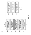
- FIG. 1 is a diagram of a circuit 100 configured to maintain a virtual voltage of a memory above a predetermined threshold regardless of a change in one or more process variables, in accordance with one or more embodiments.
- the circuit 100 includes a first signal input 101 configured to receive a first input signal, a first transistor 103 coupled to the first signal input 101 , a first line 105 , a first circuit 107 coupled to the first transistor 103 through the first line 105 , a second line 109 coupled to the first line 105 between the first transistor 103 and the first circuit 107 , a second transistor 111 coupled to the first transistor 103 through the second line 109 , a second circuit 113 coupled to the second transistor 111 , a second signal input 115 configured to receive a second input signal, a third transistor 117 coupled to the second signal input 115 and the second circuit 113 .
- the first circuit 107 is a replica of the second circuit 113 .
- the first circuit 107 is identical to the second circuit 113 .
- the first circuit 107 is a configurable replica column that is capable of replicating the function of the second circuit 113 and have the same or at least similar performance properties as the second circuit 113 .
- a virtual voltage VDDAI of the second circuit 113 is maintained above a predetermined threshold by an adaptive voltage Vclamp associated with the second line 109 .
- the voltage Vclamp associated with the second line is based, at least in part, on a difference between a first current Ibias and a second current Irep_col.
- the first current Ibias is associated with a portion of the first line 105 between the first transistor 103 and the second line 109 .
- the second current Irep_col is associated with another portion of the first line 105 between the second line 109 and the first circuit 107 . Some of the Ibias current is leaked to the first circuit 107 as Irep_col.
- the voltage Vclamp associated with the second line 109 is a clamp voltage configured to provide process variation protection, shielding, compensation, and/or immunity to the second circuit 113 .
- one or more of the first circuit 107 and the second circuit 113 is a memory.
- the memory comprises any of an SRAM, RAM, a PROM, an EPROM, a FLASH-EPROM, an EEPROM, or other suitable memory configuration.
- the second current Irep_col changes proportionally with a change in temperature
- the voltage Vclamp associated with the second line 109 changes inversely proportionally with a change in temperature
- the virtual voltage VDDAI of the second circuit 113 changes proportionally with a change in temperature thereby maintaining the virtual voltage VDDAI of the second circuit 113 above the predetermined threshold as a temperature of the second circuit 113 from a first temperature to a second temperature.
- the second current Irep_col increases, the voltage Vclamp associated with the second line 109 decreases, and the virtual voltage VDDAI of the second circuit 113 increases thereby maintaining the virtual voltage VDDAI of the second circuit 113 above the predetermined threshold as a temperature of the second circuit 113 increases from a first temperature to a second temperature.
- the first current Ibias changes inversely proportionally with a change in voltage logic
- the voltage Vclamp associated with the second line 109 changes inversely proportionally with a change in voltage logic
- the virtual voltage VDDAI of the second circuit 113 changes proportionally with a change in voltage logic thereby maintaining the virtual voltage VDDAI of the second circuit 113 above the predetermined threshold as a first signal input changes from a starting first input signal to an ending first input signal and a second signal input changes from a starting second input signal to an ending second input signal.
- the first current Ibias decreases, the voltage Vclamp associated with the second line 109 decreases, and the virtual voltage VDDAI of the second circuit 113 increases thereby maintaining the virtual voltage VDDAI of the second circuit 113 above the predetermined threshold as a first input signal changes from a starting first input signal having an ultra-low voltage logic to an ending first input signal having a standard voltage logic and a second input signal changes from a starting second input signal having an ultra-low voltage logic to an ending second input signal having a standard voltage logic.
- the first signal input 101 and the second signal input 115 are associated with a first input signal that indicates a deep sleep mode DSLP and a second input signal that indicates a deep sleep bar DSLPB (i.e., an inversion of the DSLP signal).
- the deep sleep mode DSLP and/or DSLPB are modes activated by the first input signal received by the first signal input 101 and the second input signal received by the second signal input 115 indicating a logical [1] that is indicative of the DSLP mode and, accordingly, the data retention mode.
- the data retention mode has predetermined threshold powers that are suitable for the second memory 113 in a data retention mode, such that the data retention mode is effective.
- the second circuit 113 comprises a bit line length, and the virtual voltage VDDAI of the second circuit 113 is maintained above the predetermined threshold regardless of the bit line length of the second circuit 113 .
- the first transistor 103 is a PMOS transistor.
- the second transistor 111 is a PMOS transistor and the third transistor 117 is a PMOS transistor.
- the circuit 100 further comprises a bias circuit 119 comprising one or more bias circuit transistors 121 .
- the bias circuit 119 is configured to provide a bias voltage with PVT immunity such as the voltage Vclamp.
- the bias circuit 119 is coupled to the first transistor 103 between the first signal input 101 and the first transistor 103 .
- the first current Ibias accordingly, is a bias current.
- the one or more bias circuit transistors 121 are the same type of transistor.
- the one or more bias circuit transistors are all PMOS transistors. If all of the transistors 121 are PMOS transistors, complete population of PMOS transistors reduces any variation caused by a PMOS/NMOS ratio on the performance of the circuit 100 .
- the first signal input 101 , the first transistor 103 , the first line 105 , the first circuit 107 and the second line 109 are together configured as a modular voltage clamp circuit 123 .
- the second line 109 of the voltage clamp circuit 123 is configured to be coupled to the second circuit 113 , and first circuit 107 is configurable to replicate the second circuit 113 .
- the modular voltage clamp circuit 123 is configured to maintain the virtual voltage VDDAI of the second circuit 113 above a predetermined threshold by supplying the clamp voltage Vclamp associated with the second line 109 to the second circuit 113 .
- the second circuit 113 is any type of circuit that the first circuit 107 is capable of replicating.
- the circuit 100 includes a processor such as processor 503 or a control module implemented in chip set 500 such as that discussed with respect to FIG. 5 below, in communication with one or more of the first signal input 101 , the second signal input 115 , the first circuit 107 , the second circuit 113 , to control various features of the circuit 100 and/or supply one or more signals or commands such as the first input signal received by the first signal input 101 and the second input signal received by the second signal input 115 to the circuit 100 .
- the processor or control module is in communication with the circuit 100 by any of a wired or wireless connection.
- FIG. 2 is a chart 200 illustrating the results of a simulation to determine the effectiveness of the voltage clamp circuit 123 , in accordance with one or more embodiments.
- the voltage clamp circuit 123 caused the virtual voltage VDDAI of the second circuit 113 to increase as the combination of PVT conditions goes from best to worst.
- the determined virtual voltage increase as process conditions worsened for the circuit 100 was exactly the opposite as that which would have occurred is a diode-connected PMOS transistor was used as the voltage clamp.
- FIG. 3 is a chart 300 illustrating the results of a simulation to determine the effectiveness of the voltage clamp circuit 123 , in accordance with one or more embodiments.
- performance of the circuit 100 was tested for differing bit line lengths of the second circuit 113 that ranged from 8 bits to 264 bits.
- the variation between the virtual voltage VDDAI decreased as shown in chart 300 , or less than about 5%.
- a variation of VDDAI that is less than about 5% is a significant improvement over a diode-connected PMOS transistor voltage clamp such as that discussed above which experiences a VDDAI drop of about 28%.
- FIG. 4 is a flowchart of a method 400 of maintaining a virtual voltage of a circuit above a predetermined threshold, in accordance with one or more embodiments.
- method 400 is implemented by a circuit such as a circuit including one or more components of the circuit 100 discussed above.
- method 400 is performed by a processor such as processor 503 or a control module implemented in chip set 500 such as that discussed with respect to FIG. 5 , discussed below.
- Method 400 begins with step 401 in which a first signal input receives a first input signal and communicates the first input signal to a first transistor coupled to the first signal input.
- the first input signal is a DSLP signal indicative of a data retention mode.
- the first transistor communicates the first input signal to a first line.
- the first transistor is coupled to a first circuit by the first line.
- a second signal input receives a second input signal and communicates the second input signal to a third transistor.
- the second input signal is a DSLPB signal indicative of the data retention mode.
- the third transistor is coupled to the second signal input and the second circuit.
- a clamp voltage is communicated to a second transistor through a second line.
- the second line is coupled to the first line between the first transistor and the first circuit.
- the second transistor is coupled to the first transistor through the second line.
- the clamp voltage is based, at least in part, on a difference between a first current and a second current.
- the first current is associated with a portion of the first line between the first transistor and the second line.
- the second current is associated with another portion of the first line between the second line and the first circuit.
- step 409 the second transistor communicates the clamp voltage to a second circuit, the first circuit being a replica of the second circuit.
- the second circuit is coupled to the second transistor.
- the clamp voltage supplied by to the second circuit maintains a virtual voltage of the second circuit above a predetermined threshold.
- the clamp voltage is adaptive to various process conditions and, as discussed above, is based on the difference between the first current and the second current and adapts regardless of changes in voltage logic and temperature conditions, and/or a bit line length of the second circuit to maintain the virtual voltage of the second circuit above the predetermined threshold.
- step 413 the second current changes proportionally with a change in temperature of the second circuit from a first temperature to a second temperature
- the clamp voltage changes inversely proportionally with the change in temperature of the second circuit from the first temperature to the second temperature
- the virtual voltage of the second circuit changes proportionally with the change in temperature of the second circuit from the first temperature to the second temperature, thereby maintaining the virtual voltage of the second circuit above the predetermined threshold as the temperature of the second circuit changes from the first temperature to the second temperature.
- the first current changes inversely proportionally with a change in the first input signal from a starting first input signal to an ending first input signal and a change in the second input signal from a starting second input signal to an ending second input signal
- the clamp voltage changes inversely proportionally with the change in the first input signal from the starting first input signal to the ending first input signal and the change in the second input signal from the starting second input signal to the ending second input signal
- the virtual voltage of the second circuit changes proportionally with the change in the first input signal from the starting first input signal to the ending first input signal and the change in the second input signal from the starting second input signal to the ending second input signal, thereby maintaining the virtual voltage of the second circuit above the predetermined threshold as the first voltage changes and the second voltage changes.
- the processes described herein for maintaining a virtual voltage of a circuit above a predetermined threshold by supplying a clamp voltage to the circuit may be advantageously implemented via software, hardware, firmware or a combination of software and/or firmware and/or hardware.
- the processes described herein may be advantageously implemented via processor(s), Digital Signal Processing (DSP) chip, an Application Specific Integrated Circuit (ASIC), Field Programmable Gate Arrays (FPGAs), etc.
- DSP Digital Signal Processing
- ASIC Application Specific Integrated Circuit
- FPGAs Field Programmable Gate Arrays
- FIG. 5 illustrates a chip set or chip 500 upon which or by which an embodiment is implemented.
- Chip set 500 is programmed to maintain a virtual voltage of a circuit above a predetermined threshold by supplying a clamp voltage to the circuit, as described herein, and includes, for example, bus 501 , processor 503 , memory 505 , DSP 507 and ASIC 509 components.
- the processor 503 and memory 505 are incorporated in one or more physical packages (e.g., chips).
- a physical package includes an arrangement of one or more materials, components, and/or wires on a structural assembly (e.g., a baseboard) to provide one or more characteristics such as physical strength, conservation of size, and/or limitation of electrical interaction.
- the chip set 500 are implemented in a single chip.
- the chip set or chip 500 is implemented as a single “system on a chip.” It is further contemplated that in certain embodiments a separate ASIC is not be used, for example, and all relevant functions as disclosed herein are performed by a processor or processors, e.g., processor 503 .
- Chip set or chip 500 or a portion thereof, constitutes a mechanism for performing one or more steps of maintaining a virtual voltage of a circuit above a predetermined threshold by supplying a clamp voltage to the circuit.
- the chip set or chip 500 includes a communication mechanism such as bus 501 for passing information among the components of the chip set 500 .
- Processor 503 has connectivity to the bus 501 to execute instructions and process information stored in, for example, the memory 505 .
- the processor 503 is also accompanied with one or more specialized components to perform certain processing functions and tasks such as one or more digital signal processors (DSP) 507 , or one or more application-specific integrated circuits (ASIC) 509 .
- DSP 507 typically is configured to process real-world signals (e.g., sound) in real time independently of the processor 503 .
- an ASIC 509 is configurable to perform specialized functions not easily performed by a more general purpose processor.
- Other specialized components to aid in performing the functions described herein optionally include one or more field programmable gate arrays (FPGA), one or more controllers, or one or more other special-purpose computer chips.
- FPGA field programmable gate arrays
- the processor (or multiple processors) 503 performs a set of operations on information as specified by computer program code related to maintain a virtual voltage of a circuit above a predetermined threshold by supplying a clamp voltage to the circuit.
- the computer program code is a set of instructions or statements providing instructions for the operation of the processor and/or the computer system to perform specified functions.
- the processor 503 and accompanying components have connectivity to the memory 505 via the bus 501 .
- the memory 505 includes one or more of dynamic memory (e.g., RAM, magnetic disk, writable optical disk, etc.) and static memory (e.g., ROM, CD-ROM, etc.) for storing executable instructions that when executed perform the steps described herein to maintain a virtual voltage of a circuit above a predetermined threshold by supplying a clamp voltage to the circuit.
- the memory 505 also stores the data associated with or generated by the execution of the steps.
- the memory 505 such as a random access memory (RAM) or any other dynamic storage device, stores information including processor instructions for maintaining a virtual voltage of a circuit above a predetermined threshold by supplying a clamp voltage to the circuit.
- Dynamic memory allows information stored therein to be changed by system 100 .
- RAM allows a unit of information stored at a location called a memory address to be stored and retrieved independently of information at neighboring addresses.
- the memory 505 is also used by the processor 503 to store temporary values during execution of processor instructions.
- the memory 505 is a read only memory (ROM) or any other static storage device coupled to the bus 501 for storing static information, including instructions, that is not changed by the system 100 .
- ROM read only memory
- the memory 505 is a non-volatile (persistent) storage device, such as a magnetic disk, optical disk or flash card, for storing information, including instructions, that persists even when the system 100 is turned off or otherwise loses power.
- Non-volatile media includes, for example, optical or magnetic disks.
- Volatile media include, for example, dynamic memory.
- Computer-readable media include, for example, a floppy disk, a flexible disk, hard disk, magnetic tape, any other magnetic medium, a CD-ROM, CDRW, DVD, any other optical medium, punch cards, paper tape, optical mark sheets, any other physical medium with patterns of holes or other optically recognizable indicia, a RAM, a PROM, an EPROM, a FLASH-EPROM, an EEPROM, a flash memory, any other memory chip or cartridge, or another medium from which a computer can read.
- the term computer-readable storage medium is used herein to refer to a computer-readable medium.
- One aspect of this description relates to an apparatus comprising, a first signal input, a first transistor coupled to the first signal input, a first line, a first circuit coupled to the first transistor through the first line a second line coupled to the first line between the first transistor and the first circuit a second transistor coupled to the first transistor through the second line, a second circuit coupled to the second transistor, the first circuit being a replica of the second circuit, a second signal input, and a third transistor coupled to the second signal input and the second circuit.
- the apparatus is configured to maintain a virtual voltage of the second circuit above a predetermined threshold by a voltage associated with the second line, the voltage associated with the second line being based, at least in part, on a difference between a first current and a second current, the first current being associated with a portion of the first line between the first transistor and the second line, and the second current being associated with another portion of the first line between the second line and the first circuit.
- Another aspect of this description relates to a method comprising communicating a received first input signal from a first signal input to a first transistor coupled to the first signal input.
- the method also comprises communicating the first input signal from the first transistor to a first line, the first transistor being coupled to a first circuit by the first line.
- the method further comprises communicating a clamp voltage to a second transistor through a second line, the second line being coupled to the first line between the first transistor and the first circuit, the second transistor being coupled to the first transistor through the second line, the clamp voltage being based, at least in part, on a difference between a first current and a second current, the first current being associated with a portion of the first line between the first transistor and the second line, and the second current being associated with another portion of the first line between the second line and the first circuit.
- the method additionally comprises communicating the clamp voltage from the second transistor to a second circuit coupled to the second transistor, the first circuit being a replica of the second circuit.
- the method also comprises communicating a second input signal from a second signal input to a third transistor, the third transistor being coupled to the second signal input and the second circuit.
- the method further comprises maintaining a virtual voltage of the second circuit above a predetermined threshold by supplying the clamp voltage to the second circuit.
- Still another aspect of this description relates to a voltage clamp circuit comprising a signal input, a transistor coupled to the signal input, a first line, a first circuit coupled to the transistor through the first line, and a second line coupled to the first line between the first transistor and the first circuit, the second line being configured to be coupled to a second circuit, the first circuit being configurable to replicate the second circuit.
- the signal input, the transistor, the first line, the first circuit and the second line are together configured to maintain a virtual voltage of the second circuit above a predetermined threshold by supplying a clamp voltage associated with the second line, the clamp voltage associated with the second line being based, at least in part, on a difference between a first current and a second current, the first current being associated with a portion of the first line between the first transistor and the second line, and the second current being associated with another portion of the first line between the second line and the first circuit.
Landscapes
- Engineering & Computer Science (AREA)
- Physics & Mathematics (AREA)
- Microelectronics & Electronic Packaging (AREA)
- Electromagnetism (AREA)
- General Physics & Mathematics (AREA)
- Radar, Positioning & Navigation (AREA)
- Automation & Control Theory (AREA)
- Nonlinear Science (AREA)
- Semiconductor Integrated Circuits (AREA)
Abstract
Description
Claims (20)
Priority Applications (1)
| Application Number | Priority Date | Filing Date | Title |
|---|---|---|---|
| US14/069,417 US9501079B2 (en) | 2013-11-01 | 2013-11-01 | Data retention voltage clamp |
Applications Claiming Priority (1)
| Application Number | Priority Date | Filing Date | Title |
|---|---|---|---|
| US14/069,417 US9501079B2 (en) | 2013-11-01 | 2013-11-01 | Data retention voltage clamp |
Publications (2)
| Publication Number | Publication Date |
|---|---|
| US20150123726A1 US20150123726A1 (en) | 2015-05-07 |
| US9501079B2 true US9501079B2 (en) | 2016-11-22 |
Family
ID=53006601
Family Applications (1)
| Application Number | Title | Priority Date | Filing Date |
|---|---|---|---|
| US14/069,417 Expired - Fee Related US9501079B2 (en) | 2013-11-01 | 2013-11-01 | Data retention voltage clamp |
Country Status (1)
| Country | Link |
|---|---|
| US (1) | US9501079B2 (en) |
Citations (10)
| Publication number | Priority date | Publication date | Assignee | Title |
|---|---|---|---|---|
| US5949277A (en) * | 1997-10-20 | 1999-09-07 | Vlsi Technology, Inc. | Nominal temperature and process compensating bias circuit |
| US6166590A (en) * | 1998-05-21 | 2000-12-26 | The University Of Rochester | Current mirror and/or divider circuits with dynamic current control which are useful in applications for providing series of reference currents, subtraction, summation and comparison |
| US6573780B2 (en) * | 1999-02-02 | 2003-06-03 | Macronix International Co., Ltd. | Four-phase charge pump with lower peak current |
| US20060232321A1 (en) * | 2005-04-15 | 2006-10-19 | Ibm Corporation | High-density low-power data retention power gating with double-gate devices |
| US20080074173A1 (en) * | 2006-09-25 | 2008-03-27 | Avid Electronics Corp. | Current source circuit having a dual loop that is insensitive to supply voltage |
| US7477562B2 (en) * | 2005-08-10 | 2009-01-13 | Samsung Electronics Co., Ltd. | Semiconductor memory device and a refresh clock signal generator thereof |
| US20100182850A1 (en) * | 2009-01-16 | 2010-07-22 | Shinye Shiu | Dynamic leakage control for memory arrays |
| US7777555B2 (en) * | 2008-09-18 | 2010-08-17 | Holtek Semiconductor Inc. | Temperature compensating circuit and method |
| US20120081975A1 (en) * | 2010-09-30 | 2012-04-05 | Renesas Electronics Corporation | Semiconductor integrated circuit device |
| US8390491B2 (en) * | 2011-01-14 | 2013-03-05 | Analog Devices, Inc. | Buffer to drive reference voltage |
-
2013
- 2013-11-01 US US14/069,417 patent/US9501079B2/en not_active Expired - Fee Related
Patent Citations (10)
| Publication number | Priority date | Publication date | Assignee | Title |
|---|---|---|---|---|
| US5949277A (en) * | 1997-10-20 | 1999-09-07 | Vlsi Technology, Inc. | Nominal temperature and process compensating bias circuit |
| US6166590A (en) * | 1998-05-21 | 2000-12-26 | The University Of Rochester | Current mirror and/or divider circuits with dynamic current control which are useful in applications for providing series of reference currents, subtraction, summation and comparison |
| US6573780B2 (en) * | 1999-02-02 | 2003-06-03 | Macronix International Co., Ltd. | Four-phase charge pump with lower peak current |
| US20060232321A1 (en) * | 2005-04-15 | 2006-10-19 | Ibm Corporation | High-density low-power data retention power gating with double-gate devices |
| US7477562B2 (en) * | 2005-08-10 | 2009-01-13 | Samsung Electronics Co., Ltd. | Semiconductor memory device and a refresh clock signal generator thereof |
| US20080074173A1 (en) * | 2006-09-25 | 2008-03-27 | Avid Electronics Corp. | Current source circuit having a dual loop that is insensitive to supply voltage |
| US7777555B2 (en) * | 2008-09-18 | 2010-08-17 | Holtek Semiconductor Inc. | Temperature compensating circuit and method |
| US20100182850A1 (en) * | 2009-01-16 | 2010-07-22 | Shinye Shiu | Dynamic leakage control for memory arrays |
| US20120081975A1 (en) * | 2010-09-30 | 2012-04-05 | Renesas Electronics Corporation | Semiconductor integrated circuit device |
| US8390491B2 (en) * | 2011-01-14 | 2013-03-05 | Analog Devices, Inc. | Buffer to drive reference voltage |
Also Published As
| Publication number | Publication date |
|---|---|
| US20150123726A1 (en) | 2015-05-07 |
Similar Documents
| Publication | Publication Date | Title |
|---|---|---|
| US9997252B2 (en) | High speed and low power sense amplifier | |
| CN108352175B (en) | Sense amplifier in low power high performance SRAM | |
| US9355694B2 (en) | Assist circuit for memory | |
| US10164624B2 (en) | Apparatuses for reducing off state leakage currents | |
| JP6107682B2 (en) | Semiconductor memory device and method for controlling semiconductor memory device | |
| US10199107B2 (en) | Data storage device and data refresh method thereof | |
| US9501079B2 (en) | Data retention voltage clamp | |
| TWI704562B (en) | Semiconductor device | |
| KR20160041320A (en) | Fuse circuit and semiconductor apparatus including the same | |
| KR20160056790A (en) | Integrated circuit having voltage mismatch reduction | |
| US9922691B2 (en) | Resistive memory write circuitry with bit line drive strength based on storage cell line resistance | |
| US20180047440A1 (en) | Method for autocorrective writing to a multiport static random access memory device, and corresponding device | |
| KR100335767B1 (en) | Flash memory device | |
| KR101723974B1 (en) | Operating method of non-volatile memory acquiring sensing margin using current mirror circuit | |
| JP5503433B2 (en) | Semiconductor nonvolatile memory circuit and test method thereof | |
| US20160260471A1 (en) | Semiconductor memory device | |
| JP6063003B2 (en) | Semiconductor nonvolatile memory circuit and test method thereof | |
| JP5760106B2 (en) | Semiconductor nonvolatile memory circuit and test method thereof | |
| US20230140202A1 (en) | Startup protection for standby amplifiers | |
| JP6220041B2 (en) | Semiconductor nonvolatile memory circuit and test method thereof |
Legal Events
| Date | Code | Title | Description |
|---|---|---|---|
| AS | Assignment |
Owner name: TAIWAN SEMICONDUCTOR MANUFACTURING COMPANY, LTD., Free format text: ASSIGNMENT OF ASSIGNORS INTEREST;ASSIGNORS:CHEN, CHIEN-YUAN;SHIEH, HAU-TAI;REEL/FRAME:031525/0659 Effective date: 20131023 |
|
| ZAAA | Notice of allowance and fees due |
Free format text: ORIGINAL CODE: NOA |
|
| ZAAB | Notice of allowance mailed |
Free format text: ORIGINAL CODE: MN/=. |
|
| STCF | Information on status: patent grant |
Free format text: PATENTED CASE |
|
| MAFP | Maintenance fee payment |
Free format text: PAYMENT OF MAINTENANCE FEE, 4TH YEAR, LARGE ENTITY (ORIGINAL EVENT CODE: M1551); ENTITY STATUS OF PATENT OWNER: LARGE ENTITY Year of fee payment: 4 |
|
| FEPP | Fee payment procedure |
Free format text: MAINTENANCE FEE REMINDER MAILED (ORIGINAL EVENT CODE: REM.); ENTITY STATUS OF PATENT OWNER: LARGE ENTITY |
|
| LAPS | Lapse for failure to pay maintenance fees |
Free format text: PATENT EXPIRED FOR FAILURE TO PAY MAINTENANCE FEES (ORIGINAL EVENT CODE: EXP.); ENTITY STATUS OF PATENT OWNER: LARGE ENTITY |
|
| STCH | Information on status: patent discontinuation |
Free format text: PATENT EXPIRED DUE TO NONPAYMENT OF MAINTENANCE FEES UNDER 37 CFR 1.362 |
|
| FP | Lapsed due to failure to pay maintenance fee |
Effective date: 20241122 |