US9490177B2 - Integrated circuit devices including stress proximity effects and methods of fabricating the same - Google Patents
Integrated circuit devices including stress proximity effects and methods of fabricating the same Download PDFInfo
- Publication number
- US9490177B2 US9490177B2 US13/617,582 US201213617582A US9490177B2 US 9490177 B2 US9490177 B2 US 9490177B2 US 201213617582 A US201213617582 A US 201213617582A US 9490177 B2 US9490177 B2 US 9490177B2
- Authority
- US
- United States
- Prior art keywords
- source
- drain
- finfet
- circuit
- channel region
- Prior art date
- Legal status (The legal status is an assumption and is not a legal conclusion. Google has not performed a legal analysis and makes no representation as to the accuracy of the status listed.)
- Active, expires
Links
- 238000000034 method Methods 0.000 title description 58
- 230000000694 effects Effects 0.000 title description 14
- 239000000758 substrate Substances 0.000 claims abstract description 38
- 125000006850 spacer group Chemical group 0.000 claims description 62
- 239000000463 material Substances 0.000 claims description 45
- 239000012535 impurity Substances 0.000 claims description 27
- 239000002184 metal Substances 0.000 claims description 25
- 229910052751 metal Inorganic materials 0.000 claims description 25
- 238000002955 isolation Methods 0.000 claims description 15
- 229910000577 Silicon-germanium Inorganic materials 0.000 claims description 12
- 229910052710 silicon Inorganic materials 0.000 claims description 9
- 239000010703 silicon Substances 0.000 claims description 8
- 230000005669 field effect Effects 0.000 claims description 5
- ATJFFYVFTNAWJD-UHFFFAOYSA-N Tin Chemical compound [Sn] ATJFFYVFTNAWJD-UHFFFAOYSA-N 0.000 claims description 4
- 239000012212 insulator Substances 0.000 claims description 3
- 230000003068 static effect Effects 0.000 claims description 2
- 239000004065 semiconductor Substances 0.000 description 63
- 239000010410 layer Substances 0.000 description 47
- 238000010586 diagram Methods 0.000 description 23
- VYPSYNLAJGMNEJ-UHFFFAOYSA-N Silicium dioxide Chemical compound O=[Si]=O VYPSYNLAJGMNEJ-UHFFFAOYSA-N 0.000 description 7
- 238000005530 etching Methods 0.000 description 7
- 229910052814 silicon oxide Inorganic materials 0.000 description 7
- 101150110971 CIN7 gene Proteins 0.000 description 6
- 101100286980 Daucus carota INV2 gene Proteins 0.000 description 6
- 101150110298 INV1 gene Proteins 0.000 description 6
- XUIMIQQOPSSXEZ-UHFFFAOYSA-N Silicon Chemical compound [Si] XUIMIQQOPSSXEZ-UHFFFAOYSA-N 0.000 description 6
- 101100397044 Xenopus laevis invs-a gene Proteins 0.000 description 6
- 101100397045 Xenopus laevis invs-b gene Proteins 0.000 description 6
- 239000011229 interlayer Substances 0.000 description 6
- 101100481702 Arabidopsis thaliana TMK1 gene Proteins 0.000 description 5
- 101100481704 Arabidopsis thaliana TMK3 gene Proteins 0.000 description 5
- 238000004519 manufacturing process Methods 0.000 description 5
- 229910052581 Si3N4 Inorganic materials 0.000 description 4
- MCMNRKCIXSYSNV-UHFFFAOYSA-N Zirconium dioxide Chemical compound O=[Zr]=O MCMNRKCIXSYSNV-UHFFFAOYSA-N 0.000 description 4
- HQVNEWCFYHHQES-UHFFFAOYSA-N silicon nitride Chemical compound N12[Si]34N5[Si]62N3[Si]51N64 HQVNEWCFYHHQES-UHFFFAOYSA-N 0.000 description 4
- 230000006870 function Effects 0.000 description 3
- 238000011065 in-situ storage Methods 0.000 description 3
- 238000000231 atomic layer deposition Methods 0.000 description 2
- 230000015572 biosynthetic process Effects 0.000 description 2
- 239000000969 carrier Substances 0.000 description 2
- 238000005229 chemical vapour deposition Methods 0.000 description 2
- 238000004891 communication Methods 0.000 description 2
- CJNBYAVZURUTKZ-UHFFFAOYSA-N hafnium(IV) oxide Inorganic materials O=[Hf]=O CJNBYAVZURUTKZ-UHFFFAOYSA-N 0.000 description 2
- 229910044991 metal oxide Inorganic materials 0.000 description 2
- 150000004706 metal oxides Chemical class 0.000 description 2
- 238000005240 physical vapour deposition Methods 0.000 description 2
- PBCFLUZVCVVTBY-UHFFFAOYSA-N tantalum pentoxide Inorganic materials O=[Ta](=O)O[Ta](=O)=O PBCFLUZVCVVTBY-UHFFFAOYSA-N 0.000 description 2
- 238000001039 wet etching Methods 0.000 description 2
- 229910005540 GaP Inorganic materials 0.000 description 1
- 229910001218 Gallium arsenide Inorganic materials 0.000 description 1
- 229910000673 Indium arsenide Inorganic materials 0.000 description 1
- 229910003811 SiGeC Inorganic materials 0.000 description 1
- 229910052785 arsenic Inorganic materials 0.000 description 1
- 230000000295 complement effect Effects 0.000 description 1
- 238000009792 diffusion process Methods 0.000 description 1
- 238000005516 engineering process Methods 0.000 description 1
- 229910052732 germanium Inorganic materials 0.000 description 1
- 239000011521 glass Substances 0.000 description 1
- RPQDHPTXJYYUPQ-UHFFFAOYSA-N indium arsenide Chemical compound [In]#[As] RPQDHPTXJYYUPQ-UHFFFAOYSA-N 0.000 description 1
- 238000012986 modification Methods 0.000 description 1
- 230000004048 modification Effects 0.000 description 1
- 229910003465 moissanite Inorganic materials 0.000 description 1
- 150000004767 nitrides Chemical class 0.000 description 1
- 229920002120 photoresistant polymer Polymers 0.000 description 1
- 229910021420 polycrystalline silicon Inorganic materials 0.000 description 1
- 229920005591 polysilicon Polymers 0.000 description 1
- 229910010271 silicon carbide Inorganic materials 0.000 description 1
- 238000004528 spin coating Methods 0.000 description 1
Images


Classifications
-
- H—ELECTRICITY
- H10—SEMICONDUCTOR DEVICES; ELECTRIC SOLID-STATE DEVICES NOT OTHERWISE PROVIDED FOR
- H10B—ELECTRONIC MEMORY DEVICES
- H10B10/00—Static random access memory [SRAM] devices
-
- H—ELECTRICITY
- H01—ELECTRIC ELEMENTS
- H01L—SEMICONDUCTOR DEVICES NOT COVERED BY CLASS H10
- H01L21/00—Processes or apparatus adapted for the manufacture or treatment of semiconductor or solid state devices or of parts thereof
- H01L21/70—Manufacture or treatment of devices consisting of a plurality of solid state components formed in or on a common substrate or of parts thereof; Manufacture of integrated circuit devices or of parts thereof
- H01L21/77—Manufacture or treatment of devices consisting of a plurality of solid state components or integrated circuits formed in, or on, a common substrate
- H01L21/78—Manufacture or treatment of devices consisting of a plurality of solid state components or integrated circuits formed in, or on, a common substrate with subsequent division of the substrate into plural individual devices
- H01L21/82—Manufacture or treatment of devices consisting of a plurality of solid state components or integrated circuits formed in, or on, a common substrate with subsequent division of the substrate into plural individual devices to produce devices, e.g. integrated circuits, each consisting of a plurality of components
- H01L21/822—Manufacture or treatment of devices consisting of a plurality of solid state components or integrated circuits formed in, or on, a common substrate with subsequent division of the substrate into plural individual devices to produce devices, e.g. integrated circuits, each consisting of a plurality of components the substrate being a semiconductor, using silicon technology
- H01L21/8232—Field-effect technology
- H01L21/8234—MIS technology, i.e. integration processes of field effect transistors of the conductor-insulator-semiconductor type
- H01L21/8238—Complementary field-effect transistors, e.g. CMOS
- H01L21/823821—Complementary field-effect transistors, e.g. CMOS with a particular manufacturing method of transistors with a horizontal current flow in a vertical sidewall of a semiconductor body, e.g. FinFET, MuGFET
-
- H—ELECTRICITY
- H01—ELECTRIC ELEMENTS
- H01L—SEMICONDUCTOR DEVICES NOT COVERED BY CLASS H10
- H01L27/00—Devices consisting of a plurality of semiconductor or other solid-state components formed in or on a common substrate
- H01L27/02—Devices consisting of a plurality of semiconductor or other solid-state components formed in or on a common substrate including semiconductor components specially adapted for rectifying, oscillating, amplifying or switching and having at least one potential-jump barrier or surface barrier; including integrated passive circuit elements with at least one potential-jump barrier or surface barrier
- H01L27/04—Devices consisting of a plurality of semiconductor or other solid-state components formed in or on a common substrate including semiconductor components specially adapted for rectifying, oscillating, amplifying or switching and having at least one potential-jump barrier or surface barrier; including integrated passive circuit elements with at least one potential-jump barrier or surface barrier the substrate being a semiconductor body
- H01L27/08—Devices consisting of a plurality of semiconductor or other solid-state components formed in or on a common substrate including semiconductor components specially adapted for rectifying, oscillating, amplifying or switching and having at least one potential-jump barrier or surface barrier; including integrated passive circuit elements with at least one potential-jump barrier or surface barrier the substrate being a semiconductor body including only semiconductor components of a single kind
- H01L27/085—Devices consisting of a plurality of semiconductor or other solid-state components formed in or on a common substrate including semiconductor components specially adapted for rectifying, oscillating, amplifying or switching and having at least one potential-jump barrier or surface barrier; including integrated passive circuit elements with at least one potential-jump barrier or surface barrier the substrate being a semiconductor body including only semiconductor components of a single kind including field-effect components only
- H01L27/088—Devices consisting of a plurality of semiconductor or other solid-state components formed in or on a common substrate including semiconductor components specially adapted for rectifying, oscillating, amplifying or switching and having at least one potential-jump barrier or surface barrier; including integrated passive circuit elements with at least one potential-jump barrier or surface barrier the substrate being a semiconductor body including only semiconductor components of a single kind including field-effect components only the components being field-effect transistors with insulated gate
- H01L27/092—Devices consisting of a plurality of semiconductor or other solid-state components formed in or on a common substrate including semiconductor components specially adapted for rectifying, oscillating, amplifying or switching and having at least one potential-jump barrier or surface barrier; including integrated passive circuit elements with at least one potential-jump barrier or surface barrier the substrate being a semiconductor body including only semiconductor components of a single kind including field-effect components only the components being field-effect transistors with insulated gate complementary MIS field-effect transistors
- H01L27/0924—Devices consisting of a plurality of semiconductor or other solid-state components formed in or on a common substrate including semiconductor components specially adapted for rectifying, oscillating, amplifying or switching and having at least one potential-jump barrier or surface barrier; including integrated passive circuit elements with at least one potential-jump barrier or surface barrier the substrate being a semiconductor body including only semiconductor components of a single kind including field-effect components only the components being field-effect transistors with insulated gate complementary MIS field-effect transistors including transistors with a horizontal current flow in a vertical sidewall of a semiconductor body, e.g. FinFET, MuGFET
-
- H—ELECTRICITY
- H01—ELECTRIC ELEMENTS
- H01L—SEMICONDUCTOR DEVICES NOT COVERED BY CLASS H10
- H01L29/00—Semiconductor devices adapted for rectifying, amplifying, oscillating or switching, or capacitors or resistors with at least one potential-jump barrier or surface barrier, e.g. PN junction depletion layer or carrier concentration layer; Details of semiconductor bodies or of electrodes thereof ; Multistep manufacturing processes therefor
- H01L29/66—Types of semiconductor device ; Multistep manufacturing processes therefor
- H01L29/66007—Multistep manufacturing processes
- H01L29/66075—Multistep manufacturing processes of devices having semiconductor bodies comprising group 14 or group 13/15 materials
- H01L29/66227—Multistep manufacturing processes of devices having semiconductor bodies comprising group 14 or group 13/15 materials the devices being controllable only by the electric current supplied or the electric potential applied, to an electrode which does not carry the current to be rectified, amplified or switched, e.g. three-terminal devices
- H01L29/66409—Unipolar field-effect transistors
- H01L29/66477—Unipolar field-effect transistors with an insulated gate, i.e. MISFET
- H01L29/66568—Lateral single gate silicon transistors
- H01L29/66636—Lateral single gate silicon transistors with source or drain recessed by etching or first recessed by etching and then refilled
-
- H—ELECTRICITY
- H01—ELECTRIC ELEMENTS
- H01L—SEMICONDUCTOR DEVICES NOT COVERED BY CLASS H10
- H01L29/00—Semiconductor devices adapted for rectifying, amplifying, oscillating or switching, or capacitors or resistors with at least one potential-jump barrier or surface barrier, e.g. PN junction depletion layer or carrier concentration layer; Details of semiconductor bodies or of electrodes thereof ; Multistep manufacturing processes therefor
- H01L29/66—Types of semiconductor device ; Multistep manufacturing processes therefor
- H01L29/68—Types of semiconductor device ; Multistep manufacturing processes therefor controllable by only the electric current supplied, or only the electric potential applied, to an electrode which does not carry the current to be rectified, amplified or switched
- H01L29/76—Unipolar devices, e.g. field effect transistors
- H01L29/772—Field effect transistors
- H01L29/78—Field effect transistors with field effect produced by an insulated gate
- H01L29/7842—Field effect transistors with field effect produced by an insulated gate means for exerting mechanical stress on the crystal lattice of the channel region, e.g. using a flexible substrate
- H01L29/7848—Field effect transistors with field effect produced by an insulated gate means for exerting mechanical stress on the crystal lattice of the channel region, e.g. using a flexible substrate the means being located in the source/drain region, e.g. SiGe source and drain
-
- H—ELECTRICITY
- H10—SEMICONDUCTOR DEVICES; ELECTRIC SOLID-STATE DEVICES NOT OTHERWISE PROVIDED FOR
- H10B—ELECTRONIC MEMORY DEVICES
- H10B99/00—Subject matter not provided for in other groups of this subclass
Landscapes
- Engineering & Computer Science (AREA)
- Power Engineering (AREA)
- Microelectronics & Electronic Packaging (AREA)
- Condensed Matter Physics & Semiconductors (AREA)
- General Physics & Mathematics (AREA)
- Computer Hardware Design (AREA)
- Physics & Mathematics (AREA)
- Ceramic Engineering (AREA)
- Manufacturing & Machinery (AREA)
- Crystallography & Structural Chemistry (AREA)
- Chemical & Material Sciences (AREA)
- Metal-Oxide And Bipolar Metal-Oxide Semiconductor Integrated Circuits (AREA)
- Insulated Gate Type Field-Effect Transistor (AREA)
- Electrodes Of Semiconductors (AREA)
- Semiconductor Memories (AREA)
- Thin Film Transistor (AREA)
Abstract
An integrated circuit can include first and second FETs of a particular conductivity type on a substrate, wherein a first source/drain region of the first FET is closer to a center of a first channel region of the first FET than a second source/drain region of the second FET is to a center of a second channel region of the second FET.
Description
This application claims priority from Korean Patent Application No. 10-2012-0043279 filed on Apr. 25, 2012 in the Korean Intellectual Property Office, the disclosure of which is incorporated herein by reference in its entirety.
1. Field of the Inventive Concept
The present inventive concept relates to integrated circuit devices and methods of fabricating the same.
2. Description of the Related Art
Multi-gate transistors have been suggested as one of the scaling technologies for increasing the density of a semiconductor device. In a multi-gate transistor, a fin-shaped silicon body is formed on a substrate, and a gate is formed on the surface of the silicon body.
Since the multi-gate transistor uses a 3D channel, scaling may be more easily provided. In addition, the current control capability of the multi-gate transistor can be improved even without an increase in a gate length of the multi-gate transistor. Furthermore, a short channel effect (SCE) in which the electric potential of a channel region is affected by a drain voltage can be effectively suppressed or reduced.
Embodiments according to the inventive concept can provide integrated circuit devices including stress proximity effects and methods of forming the same. Pursuant to these embodiments, an integrated circuit can include first and second FETs of a particular conductivity type on a substrate, wherein a first source/drain region of the first FET is closer to a center of a first channel region of the first FET than a second source/drain region of the second FET is to a center of a second channel region of the second FET.
In some embodiments according to the inventive concept, a first interface of the first source/drain region and the first channel region is closer to the center of the first channel region than a second interface of the second source/drain region and the second channel region is to the center of the second channel region. In some embodiments according to the inventive concept, the first and second source/drain regions can have a particular lattice constant, and wherein the first source/drain region applies greater stress to the first channel region than the second source/drain region applies to the second channel region.
In some embodiments according to the inventive concept, the first source/drain region extends past an outermost lower corner of a gate structure of the first FET into the first channel region to define an undercut region beneath the first FET, wherein the second source/drain region is aligned to a gate structure of the second FET. In some embodiments according to the inventive concept, the first and second source/drain regions can be first and second raised source/drain regions, respectively, wherein the first source/drain region extends past an outermost lower corner of a gate structure of the first FET into the first channel region to define a first undercut region beneath the first FET. The second source/drain region can extend past an outermost lower corner of a gate structure of the second FET into the second channel region to define a second undercut region beneath the second FET.
In some embodiments according to the inventive concept, the first and second source/drain regions can have different lattice constants than the first and second channel regions. In some embodiments according to the inventive concept, the first and second source/drain regions can be first and second raised source/drain regions, respectively, wherein the first raised source/drain region wraps around an outermost lower corner of a gate structure of the first FET into the first channel region to define an undercut region beneath the first FET and the second source/drain region is formed aligned to a gate structure of the second FET.
In some embodiments according to the inventive concept, the first and second source/drain regions can be first and second raised source/drain regions, respectively, wherein the first raised source/drain region wraps around an outermost lower corner of a gate structure of the first FET into the first channel region to define a first undercut region beneath the first FET and the second raised source/drain region wraps around an outermost lower corner of a gate structure of the second FET into the second channel region to define a second undercut region beneath the second FET.
In some embodiments according to the inventive concept, the device can further include a first spacer including an outer side wall of a gate structure of the first FET to provide a first thickness and a second spacer including an outer side wall of a gate structure of the second FET to provide a second thickness that is greater than the first thickness. In some embodiments according to the inventive concept, the first source/drain region is formed self-aligned to the first spacer and the second source/drain region is formed self-aligned to the second spacer. In some embodiments according to the inventive concept, a number of layers included in the first spacer is less than a number of layers included in the second spacer.
In some embodiments according to the inventive concept, the first source/drain region is formed self-aligned to the first spacer and the second source/drain region is formed self-aligned to the second spacer. In some embodiments according to the inventive concept, the first and second FETs can be PMOS FETs, the first and second channel regions include a first material that can have a first lattice constant and the first and second source/drain regions include a second material that can have a second lattice constant that is greater than the first lattice constant. In some embodiments according to the inventive concept, the first material can be Si and the second material can be SiGe.
In some embodiments according to the inventive concept, the first and second FETs can be NMOS FETs, the channel regions include a first material that can have a first lattice constant and the source/drain regions of the first and second FETs include a second material that can have a second lattice constant that is less than the first lattice constant. In some embodiments according to the inventive concept, the first material can be Si and the second material can be SiC. In some embodiments according to the inventive concept, the first and second source/drain regions are both recessed below a surface of the substrate. In some embodiments according to the inventive concept, the first and second channel regions can be respective fins that extend from the substrate to protrude from a device isolation layer to provide upper side walls and a top surface of the respective fins positioned between the first and second source/drain regions, respectively.
The above and other aspects and features of the present inventive concept will become more apparent by describing in detail exemplary embodiments thereof with reference to the attached drawings, in which:
Advantages and features of the present invention and methods of accomplishing the same may be understood more readily by reference to the following detailed description of embodiments and the accompanying drawings. The present invention may, however, be embodied in many different forms and should not be construed as being limited to the embodiments set forth herein. Rather, these embodiments are provided so that this disclosure will be thorough and complete and will fully convey the concept of the invention to those skilled in the art, and the present invention will only be defined by the appended claims. Thus, in some embodiments, well-known methods, procedures, components, and circuitry have not been described in detail to avoid unnecessarily obscuring aspects of the present invention.
It will be understood that, although the terms first, second, etc. may be used herein to describe various elements, components, regions, layers and/or sections, these elements, components, regions, layers and/or sections should not be limited by these terms. These terms are only used to distinguish one element, component, region, layer or section from another element, component, region, layer or section. Thus, a first element, component, region, layer or section discussed below could be termed a second element, component, region, layer or section without departing from the teachings of the present invention.
The terminology used herein is for the purpose of describing particular embodiments only and is not intended to be limiting of the invention. As used herein, the singular forms “a,” “an” and “the” are intended to include the plural forms as well, unless the context clearly indicates otherwise. It will be further understood that the terms “comprises,” “comprising,” “includes” and/or “comprising,” when used in this specification, specify the presence of the stated features, integers, steps, operations, elements, and/or components, but do not preclude the presence or addition of one or more other features, integers, steps, operations, elements, components, and/or groups thereof.
Unless otherwise defined, all terms (including technical and scientific terms) used herein have the same meaning as commonly understood by one of ordinary skill in the art to which this invention belongs. It will be further understood that terms, such as those defined in commonly used dictionaries, should be interpreted as having a meaning that is consistent with their meaning in the context of the relevant art and will not be interpreted in an idealized or overly formal sense unless expressly so defined herein.
Referring to FIGS. 1 through 3 , a first fin transistor 101 is formed in a first region I, and a second fin transistor 201 is formed in a second region II. The first region I and the second region II may be separated or connected. The first region I may be, for example, a static random access memory (SRAM) region, and the second region II may be a logic region. Alternatively, the first region I may be a region in which a pull-up transistor of an SRAM is formed, and the second region II may be a region in which a pull-down transistor or a pass transistor of the SRAM is formed.
The first fin transistor 101 has a first stress proximity, and the second fin transistor 201 has a second stress proximity which is different from the first stress proximity. Appropriate stress applied to a channel (by, for example, different lattice constants) may improve the mobility of carriers and increase the amount of current. As appreciated by the present inventive step, how closely stress is applied to the channel (such as relative to a center of the channel) may determine the amount of strain on the channel. This is called a proximity effect. Various methods can be used to make the first fin transistor 101 and the second fin transistor 201 have different stress proximities. In the semiconductor device shown in FIGS. 1-3 , according to an embodiment of the present inventive concept, a first distance L1 between a first gate electrode 147 and a first source/drain 161 (e.g., first source/drain region) and a second distance L2 between a second gate electrode 247 and a second source/drain 261 (e.g., second source/drain region) are adjusted to be different from each other, such that the first stress proximity and the second stress proximity are different from each other.
It will be understood that the stress proximity effects discussed herein can also be specified relative to a position in the channel region associated with a respective source/drain region. For example, as shown in FIG. 3 , the stress proximity effects can also be specified by a distance from the respective source/drain region to a center of the channel region associated with the same fin transistor 201. In particular, the first fin transistor 101 can experience a stress proximity effect that is defined by the distance between the first source/drain region 161 and a center of the channel region for the first fin transistor 101. Similarly, the second fin transistor 101 can experience a separate stress proximity effect that is defined by the distance from the second source/drain region 261 to a center of the channel region associated with the second fin transistor 201. Accordingly, the stress proximity effects for the respective fin transistors 101 and 201 can be specified by the distances L3 and L4 rather than the distances L1 and L2.
It will be further understood that the reference point for the stress proximity effects can be defined relative to the interface between the source/drain region and the channel region associated with the respective transistor. For example, as described above, the distance L1 or L3 that is shown associated with the first fin transistor 101 can be shown relative to the first source/drain region 161, which can be more particularly defined by an interface location where the first source/drain region 161 ends and the channel region associated with the first fin transistor 101 begins. It will be understood that although this reference location is defined as an interface, the actual location may actually not be a particular location, as the source/drain and channel regions may not define a clearly marked boundary but rather are subject to the device physics associated with the diffusion of impurities. It will be understood, however, that the interface location should be interpreted as being a consistent reference point applied to the different transistors.
The first fin transistor 101 may include a first fin F1, the first gate electrode 147, a first recess 125, and the first source/drain 161.
The first fin F1 may extend along a second direction Y1. The first fin F1 may be a part of a substrate 100 and may include an epitaxial layer grown from the substrate 100. An element isolation film 110 may cover lower side walls of the first fin F1 whereas upper side walls of the first fin F1 are exposed.
The first gate electrode 147 may be formed on the first fin F1 to intersect the first fin F1. The first gate electrode 147 may extend in a first direction X1.
The first gate electrode 147 may include metal layers MG1 and MG2. As shown in the drawings, the first gate electrode 147 may include a stack of two or more metal layers MG1 and MG2. A first metal layer MG1 can control a work function, and a second metal layer MG2 fills a space formed by the first metal layer MG1. The first metal layer MG1 may include at least one of, e.g., TiN, TaN, TiC and TaC. In addition, the second metal layer MG2 may include W or Al. Alternatively, the first gate electrode 147 may be made of Si, SiGe, or the like rather than a metal. The first gate electrode 147 may be formed using a replacement process, however, other processes may be used.
A first gate insulating film 145 may be formed between the first fin F1 and the first gate electrode 147. Referring to FIG. 2 , the first gate insulating film 145 may be formed on top and side surfaces of the first fin F1. In addition, the first gate insulating film 145 may be disposed between the first gate electrode 147 and the element isolation film 110. The first gate insulating film 145 may include a high-k material having a higher dielectric constant than a silicon oxide film. For example, the first gate insulating film 145 may include HfO2, ZrO2, or Ta2O5.
The first recess 125 may be formed in the first fin F1 on both sides of the first gate electrode 147. The first recess 125 may have sloping side walls. Thus, the first recess 125 may become wider as the distance from the substrate 100 increases. As shown in FIG. 1 , the first recess 125 may be wider than the first fin F1.
The first source/drain 161 is formed in the first recess 125. The first source/drain 161 may be an elevated source/drain. That is, a top surface of the source/drain 161 may be higher than an upper surface of a first interlayer insulating film 155. In addition, the first source/drain 161 and the first gate electrode 147 may be insulated from each other by a spacer 151.
When the first fin transistor 101 is a p-channel metal oxide (PMOS) transistor, the first source/drain 161 may include a compressive stress material. The compressive stress material may be a material (e.g., SiGe) having a lattice constant that is greater than that of Si. The compressive stress material may apply compressive stress to the first fin F1, thereby improving the mobility of carriers in a channel region.
On the other hand, when the first fin transistor 101 is an n-channel metal oxide semiconductor (NMOS) transistor, the first source/drain 161 may be the same material as the substrate 100 or a tensile stress material. For example, when the substrate 100 is Si, the first source/drain 161 may be Si or a material (e.g., SiC) having a lattice constant that is less than that of Si.
The spacer 151 may include at least one of a nitride film and an oxynitride film.
The substrate 100 may be made of one or more semiconductor materials selected from the group consisting of Si, Ge, SiGe, GaP, GaAs, SiC, SiGeC, InAs, and InP. The substrate 100 can also be a silicon-on-insulator (SOI) substrate.
The second fin transistor 201 may include a second fin F2, the second gate electrode 247, a second recess 225, and the second source/drain 261. The second gate electrode 247 may be formed on the second fin F2 to intersect the second fin F2, the second recess 225 may be formed in the second fin F2 on both sides of the second gate electrode 247, and the second source/drain 261 may be formed in the second recess 225. The second fin transistor 201 is overall similar to the first fin transistor 101, and thus differences from the first fin transistor 101 will mainly be described below.
In FIG. 1 , the first fin F1 and the second fin F2 extend parallel to each other in the second direction Y1 and Y2. However, this illustration is merely for ease of description, and the present inventive concept is not limited thereto. For example, the first fin F1 may extend along the second direction Y1, and the second fin F2 may extend along the first direction X2.
Likewise, while the first gate electrode 147 and the second gate electrode 247 extend parallel to each other along the first direction X1 and X2 in FIG. 1 , the present inventive concept is not limited thereto. For example, the first gate electrode 147 may extend along the first direction X1, and the second gate electrode 247 may extend along the second direction Y2.
The first fin transistor 101 and the second fin transistor 201 may be of the same conductivity type (e.g., a P type or an N type) sometimes referred to herein as a particular conductive type. Alternatively, the first fin transistor 101 may be of a first conductivity type (e.g., the P type), and the second fin transistor 201 may be of a second conductivity type (e.g., the N type).
The reference numeral 200 indicates a substrate, reference numeral 245 indicates a second gate insulating film, reference numeral 251 indicates a second spacer, reference numeral 255 indicates a second interlayer insulating film, reference character MG3 indicates a third metal layer, and reference character MG4 indicates a fourth metal layer.
Referring to FIG. 3 , as described above, the first stress proximity effect in the first fin transistor 101 is different from the second stress proximity effect in the second fin transistor 201. Specifically, the first distance L1 between the first gate electrode 147 and the first source/drain 161 is different from the second distance L2 between the second gate electrode 247 and the second source/drain 261, Here, ‘a distance between a and b’ denotes a shortest distance between a and b. As shown in the drawing, the second distance L2 may be shorter than the first distance L1.
As described above the distances L3 and L4 are alternatively used to illustrate that the different stress proximity effects in the first fin transistor 101 and the second fin transistor 201 can be specified by the distance between the respective source/drain region and the center of the channel of the respective transistor, rather than specifying between the source/drain region and a particular portion of the gate electrode of the respective first or second fin transistor 101 and 201.
As further shown in FIG. 3 , the distances L2/L4 are less than L1/L3 respectively in that the interface of the second source/drain region 261 and the channel region associated with second fin transistor 201 extends past an outer most lower corner of the respective second gate electrode 247 into the second channel region to define an undercut region beneath the second fin transistor 201.
Since the first recess 125 and the second recess 225 are respectively formed in the first source/drain 161 and the second source/drain 261, the first distance L1/L3 and the second distance L2/L4 can be adjusted by adjusting the positions of the first recess 125 and the second recess 225.
For example, if both of the first fin transistor 101 and the second fin transistor 201 are P-type transistors, the substrate 100 may be Si, and the first source/drain 161 and the second source/drain 261 may be SiGe. In this case, since SiGe has a greater lattice constant than Si, the first source/drain 161 may apply compressive stress to the channel region of the first fin transistor 101, and the second source/drain 261 may apply compressive stress to the channel region of the second fin transistor 201. However, since the first distance L1/L3 is longer than the second distance L2/L4, the compressive stress applied to the channel region of the first fin transistor 101 by the first source/drain 161 may be less than the compressive stress applied to the channel region of the second fin transistor 201 by the second source/drain 261. Accordingly, the first fin transistor 101 may have less current than the second fin transistor 201.
When a fin having a very small width (e.g., a width of 20 nm or less) is formed, a conventional photo process may not be used. For example, a sidewall image transfer (SIT) process in which a fin with a predetermined width is formed repeatedly may be used. In this case, it may be more difficult to adjust an effective channel width. That is, in the case of a conventional planar transistor, the amount of current can be more readily adjusted by changing the channel width using a photo process. However, in the case of a fin transistor using fins formed by the SIT process, it may be more difficult to adjust the amount of current since the channel width is fixed. That is, the amount of current can be adjusted only by changing the number of fins. For example, when one fin is used, the amount of current of a fin transistor is k. When two fins are used, the amount of current of the fin transistor is 2 k. That is, it is difficult to finely adjust the amount of current.
In the semiconductor device according to the first embodiment of the present inventive concept, however, the current of the first and second fin transistors 101 and 201 can be controlled by adjusting the first and second distances L1/L3 and L2/L4 between the first and second gate electrodes 147 and 247 (or centers of respective channel regions) and the first and second sources/drains 161 and 261.
Referring to FIG. 4 , a first distance L1/L3 between a first gate electrode 147 (or the center of the channel region) and a first source/drain 161 in a first fin transistor 102 is different from a second distance L2/L4 between a second gate electrode 247 (or the center of the channel region) and a second source/drain 261 in a second fin transistor 202. An amount of undercut of a first recess 125 is different from an amount of undercut of a second recess 225. As shown in the drawing, the amount of undercut of the second recess 225 is greater than that of the first recess 125. Therefore, even though both source/drain regions exhibit undercut, the undercut of the second source/drain region 261 is greater.
Further, a first stress film 169 may be formed on the first fin transistor 102, and a second stress film 269 may be formed on the second fin transistor 202.
Each of the first stress film 169 and the second stress film 269 may be, for example, a SiN film. Whether the SiN film applies tensile stress or compressive stress is determined by a ratio of N—H bonding to Si—H bonding in the SiN film. For example, the SiN film may apply the tensile stress when the ratio of N—H bonding/Si—H bonding is approximately 1 to 5 and apply the compressive stress when the ratio of N—H bonding/Si—H bonding is approximately 5 to 20.
For example, if both of the first fin transistor 102 and the second fin transistor 202 are PMOS transistors, the current of the second fin transistor 202 may be greater than the current of the first fin transistor 102. The first stress film 169 and the second stress film 269 may have the effect of increasing the current of both the first fin transistor 102 and the second fin transistor 202.
Referring to FIG. 5A , a first spacer 151 is disposed on sidewalls of a first gate electrode 147 of a first fin transistor 103. In addition, a second spacer 251 is disposed on sidewalls of a second gate electrode 247 of a second fin transistor 203. As shown in the drawing, a first thickness of the first spacer 151 is different from a second thickness of the second spacer 251.
To make the first spacer 151 and the second spacer 251 have different thicknesses, the first spacer 151 may include n (where n is a natural number) layers, and the second spacer 251 may include (n+m) (where m is a natural number) layers. In the drawing, the first spacer 151 includes two insulating layers 151 a and 151 b, and the second spacer 251 includes three insulating layers 251 a, 251 b and 251 c.
A first recess 125 may be formed using the first spacer 151 as a mask, and a second recess 225 may be formed using the second spacer 251 as a mask. That is, the first recess 125 may be aligned with the first spacer 151, and the second recess 225 may be aligned with the second spacer 251. However, the present inventive concept is not limited thereto. The first recess 125 may include an undercut and extend to under the first spacer 151, and the second recess 225 may include an undercut and extend to under the second spacer 251 as described herein in reference to FIGS. 3 and 4 .
Since the first spacer 151 and the second spacer 251 have different thicknesses, the first recess 125 and the second recess 225 may be located at different positions. As shown in the drawing, since the second spacer 251 is thicker than the first spacer 151, a second distance L2/L4 may be greater than a first distance L1/L3. In this case, if both of the first fin transistor 103 and the second fin transistor 203 are PMOS transistors, the first fin transistor 103 may have a greater amount of current than the second fin transistor 203.
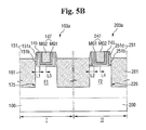
Referring to FIG. 5B , a distance L1/L3 between a first gate electrode 147 (or center of the channel region) and a first source/drain 161 in a first fin transistor 103 a may be equal to a distance L2/L4 between a second gate electrode 247 (or center of the channel region) and a second source/drain 261 in a second fin transistor 203 a.
Stress applied to a channel of the first fin transistor 103 a by a first spacer 151 may be different from stress applied to a channel of the second fin transistor 203 a by a second spacer 251. For example, different materials may be used to form the first spacer 151 and the second spacer 251. Specifically, insulating layers 151 a and 151 b of the first spacer 151 and an insulating layer 251 b of the second spacer 251 may not be materials that apply stress to a channel. However, an insulating layer 251 d of the second spacer 251 may be a material that applies stress to the channel of the second fin transistor 203 a. As a result, an amount of current of the first fin transistor 103 a may be different from an amount of current of the second fin transistor 203 a.
Referring to FIG. 6 , a first distance L1/L3 associated with a first fin transistor 104 may be substantially equal to a second distance L2/L4 associated with a second fin transistor 204.
Here, the first fin transistor 104 and the second fin transistor 204 are of the same conductivity type, and an impurity concentration of a source/drain 161 formed in a first recess 125 is different from an impurity concentration of a second source/drain 261 formed in a second recess 225. For example, when the impurity concentration of the second source/drain 261 is greater than that of the first source/drain 161, a resistance of the second source/drain 261 may be less than that of the first source/drain 161. Accordingly, the second fin transistor 204 may have a greater amount of current than the first fin transistor 104. That is, the amount of current can be adjusted by controlling the impurity concentration of each of the first source/drain 161 and the second source/drain 261.
Referring to FIG. 7 , in the semiconductor device according to an embodiment of the present inventive concept, an amount of current of a fin transistor can be adjusted using a combination of features (such as adjusting a distance between a gate electrode or a center of a channel region and a source/drain (or a source/drain channel interface), adjusting the impurity concentration, and using a stress film).
That is, a first spacer 151 is disposed on sidewalls of a first gate electrode 147 of a first fin transistor 105, and a second spacer 251 is disposed on sidewalls of a second gate electrode 247 of a second fin transistor 205. A first thickness of the first spacer 151 is different from a second thickness of the second spacer 251.
In addition, an impurity concentration of the first source/drain 161 formed in a first recess 125 is different from an impurity concentration of the second source/drain 261 formed in a second recess 225.
Further, a first stress film 169 may be formed on the first fin transistor 105, and a second stress film 269 may be formed on the second fin transistor 205.
In FIG. 7 , a case where the impurity concentration of the first source/drain 161 is different from the impurity concentration of the second source/drain 261 is illustrated as an example. However, the present inventive concept is not limited to this case. For example, the concentration of a material (e.g., SiGe) that fills the first source/drain 161 may be different from the concentration of a material that fills the second source/drain 261. In this case, stress applied to a channel of the first fin transistor 105 may also be different from stress applied to a channel of the second fin transistor 205.
Referring to FIG. 8 , the semiconductor device according to the sixth embodiment of the present inventive concept may include a pair of inverters INV1 and INV2 connected in parallel between a power supply node Vcc and a ground node Vss and first and second pass transistors PS1 and PS2 connected respectively to output nodes of the inverters INV1 and INV2. The first pass transistor PS1 and the second pass transistor PS2 may be connected to a bit line BL and a complementary bit line BL/, respectively. A gate of the first pass transistor PS1 and a gate of the second pass transistor PS2 may be connected to a word line WL.
A first inverter INV1 includes a first pull-up transistor PU1 and a first pull-down transistor PD1 connected in series to each other, and a second inverter INV2 includes a second pull-up transistor PU2 and a second pull-down transistor PD2 connected in series to each other. The first pull-up transistor PU1 and the second pull-up transistor PU2 may be PMOS transistors, and the first pull-down transistor PD1 and the second pull-down transistor PD2 may be NMOS transistors.
In addition, an input node of the first inverter INV1 is connected to an output node of the second inverter INV2, and an input node of the second inverter INV2 is connected to an output node of the first inverter INV1, so that the first inverter INV1 and the second inverter INV2 form one latch circuit.
Referring to FIGS. 8 through 10B , first through fourth fins 310 through 340 are separated from each other and extend in a direction (e.g., a vertical direction in FIG. 9 ). The second fin 320 and the third fin 330 may be shorter than the first fin 310 and the fourth fin 340.
In addition, first through fourth gate electrodes 351 through 354 extend in the other direction (e.g., a horizontal direction in FIG. 9 ) and intersect the first through fourth fins 310 through 340. Specifically, the first gate electrode 351 may completely intersect the first fin 310 and the second fin 320 and overlap an end of the third fin 330. The third gate electrode 353 may completely intersect the fourth fin 340 and the third fin 330 and overlap an end of the second fin 320. The second gate electrode 352 and the fourth gate electrode 354 intersect the first fin 310 and the fourth fin 340, respectively.
As shown in the drawings, the first pull-up transistor PU1 is defined in a region in which the first gate electrode 351 intersects the second fin 320, the first pull-down transistor PD1 is defined in a region in which the first gate electrode 351 intersects the first fin 310, and the first pass transistor PS1 is defined in a region in which the second gate electrode 352 intersects the first fin 310. The second pull-up transistor PU2 is defined in a region in which the third gate electrode 353 intersects the third fin 330, the second pull-down transistor PD2 is defined in a region in which the third gate electrode 353 intersects the fourth fin 340, and the second pass transistor PS2 is defined in a region in which the fourth gate electrode 354 intersects the fourth fin 340.
A recess may be formed on both sides of each of the regions in which the first through fourth gate electrodes 351 through 354 intersect the first through fourth fins 310 through 340, and a source/drain may be formed in the recess. A plurality of contacts 350 may be formed.
Furthermore, a shared contact 361 connects all of the second fin 320, a third gate electrode 353, and a wiring 371. A shared contact 362 connects all of the third fin 330, the first gate electrode 351, and a wiring 372.
The first pull-up transistor PU1, the first pull-down transistor PD1, the first pass transistor PS1, the second pull-up transistor PU2, the second pull-down transistor PD2, and the second pass transistor PS2 may all be implemented as fin transistors and may be configured as described above with reference to, for example, FIGS. 1 through 7 .
For example, the above transistors may be configured as shown in FIG. 10B . The first pull-up transistor PU1 may include the second fin 320, the first gate electrode 351 which intersects the second fin 320, a first recess 321 a which is formed in the second fin 320 on both sides of the first gate electrode 351, and a first source/drain 321 which is formed in the first recess 321 a. The first pull-down transistor PD1 may include the first fin 310, the first gate electrode 351 which intersects the first fin 310, a second recess 311 a which is formed in the first fin 310 on both sides of the first gate electrode 351, and a second source/drain 311 which is formed in the second recess 311 a.
In this case, a distance L3/L5 between the first gate electrode 351 (or center of the channel region) and the first source/drain 321 of the first pull-up transistor PU1 may be different from a distance L4/L6 between the first gate electrode 351 (or center of the channel region) and the second source/drain 311 of the first pull-down transistor PD1. To reduce the consumption of current, for example, an amount of current of the first pull-up transistor PU1 may be reduced. Therefore, the distance L3/L5 may be greater than the distance L4/L6.
The first pass transistor PS1 may include the first fin 310, the second gate electrode 352 which intersects the first fin 310, a third recess which is formed in the first fin 310 on both sides of the second gate electrode 352, and a third source/drain which is formed in the third recess. As shown in the drawings, the second source/drain and the third source/drain share one node. The distance L3/L5 between the first gate electrode 351 (or center of the channel region) and the first source/drain 321 of the first pull-up transistor PU1 may be different from a distance between the second gate electrode 352 (or center of the channel region) and the third source/drain of the first pass transistor PS1. In addition, the distance L3/L5 between the first gate electrode 351 (or center of the channel region) and the first source/drain 321 of the first pull-up transistor PU1 may be longer than the distance between the second gate electrode 352 (or center of the channel region) and the third source/drain of the first pass transistor PS1.
Referring to FIG. 10A , a process of forming recesses in the first pull-up transistor PU1 and the second pull-up transistor PU2 of a first region I may be performed separately from a process of forming recesses in the first pull-down transistor PD1, the second pull-down transistor PD2, the first pass transistor PS1, and the second pass transistor PS2 of a second region II.
In so doing, the amount of current of the first pull-up transistor PU1 and the second pull-up transistor PU2 can be reduced.
Referring to FIG. 11A , in the semiconductor device according to the embodiment of the present inventive concept, a fin transistor 411 may be disposed in a logic region 410, and a fin transistor 421 may be disposed in an SRAM region 420.
A distance between a gate electrode (or center of a channel region) and a source/drain of the fin transistor 411 and a distance between a gate electrode (or center of the channel region) and a source/drain of the fin transistor 421 may be adjusted to be different. Moreover, stress applied to a channel of the fin transistor 411 and stress applied to a channel of the fin transistor 421 may be adjusted to be different.
In FIG. 11A , the logic region 410 and the SRAM region 420 are illustrated as an example. However, the present inventive concept is not limited to this example. The present inventive concept is also applicable to a case where the logic region 410 and a region in which another memory (e.g., DRAM, MRAM, RRAM, PRAM, or the like) is formed are provided.
Referring to FIG. 11B , in the semiconductor device according to the embodiment of the present inventive concept, different fin transistors 412 and 422 may be disposed in a logic region 410.
That is, a distance between a gate electrode (or center of the channel region) and a source/drain of the fin transistor 412 and a distance between a gate electrode (or center of the channel region) and a source/drain of the fin transistor 422 may be adjusted to be different. Moreover, stress applied to a channel of the fin transistor 412 and stress applied to a channel of the fin transistor 422 may be adjusted to be different.
Referring to FIG. 11C , in the semiconductor device according to the embodiment of the present inventive concept, a plurality of blocks, e.g., BLK1 and BLK2 are defined in a substrate. Here, different fin transistors may be disposed in each of the blocks BLK1 and BLK2. As shown in the drawing, one or more fins F5 or F6 may be disposed in each of the blocks BLK1 and BLK2. A distance between a gate electrode (or center of the channel region) and a source/drain of a fin transistor disposed in the block BLK1 and a distance between a gate electrode (or center of the channel region) and a source/drain of a fin transistor disposed in the block BLK2 may be adjusted to be different. Moreover, stress applied to a channel of the fin transistor disposed in the block BLK1 and stress applied to a channel of the fin transistor disposed in the block BLK2 may be adjusted to be different.
Referring to FIG. 12 , in the semiconductor device according to the embodiment of the present inventive concept, an amount of current of a fin transistor 106 or 106 a is adjusted by controlling the number of fins F11 and F12 or F21 and F22 used.
The fin transistor 106 includes a plurality of first fins F11 and F12 which are separated from each other and parallel to each other. A first gate electrode 147 may intersect the first fins F11 and F12. The fin transistor 106 a includes a plurality of second fins F21 and F22 which are separated from each other and parallel to each other. A second gate electrode 247 may intersect the second fins F21 and F22.
A distance between the first gate electrode 147 (or center of the channel region) and a source/drain of the fin transistor 106 may be different from a distance between the second gate electrode 247 (or center of the channel region) and a source/drain of the fin transistor 106 a. Additionally or alternatively, an impurity concentration of the source/drain of the fin transistor 106 may be different from an impurity concentration of the source/drain of the fin transistor 106 a.
When the number of fins F11 and F12 used by the fin transistor 106 increases, the amount of current may increase. That is, if the amount of current of the fin transistor 106 is j when one fin is used, it becomes 2j when two fins F11 and F12 are used. In addition, as described above, the amount of current of the fin transistor 106 a may be adjusted to be a little different from the amount of current of the fin transistor 106. For example, the amount of current of the fin transistor 106 a may be approximately 2j+α or 2j−α.
Therefore, according to the embodiment of the present inventive concept, fin transistors 106 and 106 a having various amounts of current can be implemented.
Referring to FIG. 13 , in the semiconductor device according to the embodiment of the present inventive concept, amounts of current of fin transistors 108, 107, 106 and 101 can be adjusted by controlling the number of fins F1 a, F1 b, F2 a, F2 b, F3 a, F3 b, F4 a, and F4 b used.
Therefore, according to the embodiment of the present inventive concept, fin transistors 108, 108 a, 107, 107 a, 106, 106 a, 101 and 101 a having various amounts of current can be implemented.
Referring to FIG. 14 , a first fin F1 is formed in a first region I. Specifically, a mask pattern 2103 is formed on a substrate 100, and then an etching process is performed to form the first fin F1. The first fin F1 may extend along a second direction Y1. A trench 121 is formed around the first fin F1. The mask pattern 2103 may be made of a material that includes at least one of a silicon oxide film, a silicon nitride film, and a silicon oxynitride film.
Referring to FIG. 15 , an element isolation film 110 is formed to fill the trench 121. The element isolation film 110 may be made of a material that includes at least one of a silicon oxide film, a silicon nitride film, and a silicon oxynitride film.
Referring to FIG. 16 , an upper part of the element isolation film 110 is recessed to expose an upper part of the first fin F1 including upper sidewalls thereof. The recess process may include a selective etching process. The mask pattern 2103 may be removed before or after the formation of the element isolation film 110.
A part of the first fin F1 which protrudes upward from the element isolation film 110 may be formed by an epitaxial process. Specifically, after the element isolation film 110 is formed, an epitaxial process may be performed using a top surface of the first fin F1, which is exposed by the element isolation film 110, as a seed. As a result, the protruding part of the first fin F1 (including the upper side walls) may be formed without a recess process.
In addition, a doping process for controlling a threshold voltage may be performed on the first fin F1. When the first fin transistor 101 is an NMOS transistor, impurities may be B. When the first fin transistor 101 is a PMOS transistor, the impurities may be P or As.
Referring to FIG. 17 , an etching process is performed using a mask pattern 2104, thereby forming a dummy gate insulating film 141 and a first dummy gate electrode 143 which intersect the first fin F1 and extend in a first direction X1.
For example, the dummy gate insulating film 141 may be a silicon oxide film, and the first dummy gate electrode 143 may be polysilicon.
Referring to FIG. 18 , a first spacer 151 is formed on side walls of the first dummy gate electrode 143 and upper side walls of the first fin F1.
For example, an insulating layer may be formed on the resultant structure (of FIG. 17 ) having the first dummy gate electrode 143, and then an etch-back process may be performed, thereby forming the first spacer 151. The first spacer 151 may expose a top surface of the mask pattern 2104 and the top surface of the first fin F1. The first spacer 151 may be a silicon nitride film or a silicon oxynitride film.
Referring to FIG. 19 , an interlayer insulating film 155 is formed on the resultant structure (of FIG. 18 ) having the first spacer 151. The interlayer insulating film 155 may be a silicon oxide film.
Next, the interlayer insulating film 155 is planarized until a top surface of the first dummy gate electrode 143 is exposed. As a result, the mask pattern 2104 is removed, thereby exposing the top surface of the first dummy gate electrode 143.
Referring to FIG. 20 , the dummy gate insulating film 141 and the first dummy gate electrode 143 are removed. The removal of the dummy gate insulating film 141 and the first dummy gate electrode 143 results in the formation of a trench 123 which exposes the element isolation film 110.
Referring to FIGS. 21 through 23 , a first gate insulating film 145 and a first gate electrode 147 are formed in the trench 123.
The first gate insulating film 145 may include a high-k material having a higher dielectric constant than a silicon oxide film. The first gate insulating film 145 may include, for example, HfO2, ZrO2, or Ta2O5. The first gate insulating film 145 may be substantially conformally formed along sidewalls and a bottom surface of the trench 123.
The first gate electrode 147 may include metal layers MG1 and MG2. As shown in the drawings, the first gate electrode 147 may include a stack of two or more metal layers MG1 and MG2. A first metal layer MG1 controls a work function, and a second metal layer MG2 fills a space formed by the first metal layer MG1. The first metal layer MG1 may include at least one of e.g., TiN, TaN, TiC and TaC. In addition, the second metal layer MG2 may include W or Al. Alternatively, the first gate electrode 147 may be made not of metal but of Si, SiGe, or the like.
In the same way as described above, a second gate insulating film 245 and a second gate electrode 247 are formed in a second region II. The second gate electrode 247 may include metal layers MG3 and MG4.
Referring to FIGS. 24 through 26 , a first recess 125 is formed in the first fin F1 on both sides of the first gate electrode 147 in the first region I, and a second recess 225 is formed in a second fin F2 on both sides of the second gate electrode 247 in the second region II.
Here, the first recess 125 and the second recess 225 may be formed such that a first distance L1/L3 between the first gate electrode 147 (or center of the channel region) and the first recess 125 is different from a second distance L2/L4 between the second gate electrode 247 (or center of the channel region) and the second recess 225. The forming of the first recess 125 may be performed separately from the forming of the second recess 225.
For example, a first wet-etching process may be performed for a first period of time using a first mask which exposes the first region I but does not expose the second region II. Then, a second wet-etching process may be performed for a second period of time which is different from the first period of time using a second mask which exposes the second region II but does not expose the first region I.
Additionally or alternatively, an etchant used to form the first recess 125 may be different from an etchant used to form the second recess 225.
For example, the first recess 125 may not include an undercut, and the second recess 225 may include an undercut. Alternatively, an amount of undercut of the first recess 125 and an amount of undercut of the second recess 225 may be adjusted to be different. Accordingly, the first distance L1/L3 and the second distance L2/L4 may become different.
Referring to FIGS. 1 through 3 , a first source/drain 161 is formed in the first recess 125, and a second source/drain 261 is formed in the second recess 225. The first source/drain 161 may be, for example, an elevated source/drain. That is, a top surface of the first source/drain 161 may be higher than a bottom surface of the first interlayer insulating film 155.
The forming of the first source/drain 161 and the forming of the second source/drain 261 may be achieved by an epitaxial process. In addition, the material that forms the first source/drain 161 and the second source/drain 261 may vary according to whether the first fin transistor 101 and the second fin transistor 201 are PMOS transistors or NMOS transistors.
Impurities may be doped in situ during the epitaxial process.
Referring to FIG. 27 , n (where n is a natural number) insulating layers 451 a and 451 b are formed on a first region I and a second region II. In the drawing, a case where n is two is illustrated. However, the present inventive concept is not limited to this case.
Referring to FIG. 28 , the two insulating layers 451 a and 451 b are etched back using a first mask 460 which exposes the first region I but does not expose the second region II. As a result, a first spacer 151 is formed on sidewalls of a first dummy gate electrode 143. Then, the first mask 460 is removed.
Referring to FIG. 29 , a second mask 470 which exposes the second region II but does not expose the first region I is formed. Then, m (where, m is a natural number) insulating layers 451 c are formed on the second region II. In the drawing, a case where m is one is illustrated as an example. However, the present inventive concept is not limited to this case.
Referring to FIG. 30 , the insulating layers 451 a, 451 b and 451 c are etched back using the second mask 470. As a result, a second spacer 251 is formed on sidewalls of a second dummy gate electrode 243.
In summary, to make the first spacer 151 of the first region I and the second spacer 251 of the second region II have different thicknesses, the first spacer 151 is formed by etching back n insulating layers 451 a and 451 b formed on the first region I. Then, the second spacer 251 is formed by etching back (n+m) insulating layers 451 a, 451 b and 451 c formed on the second region II.
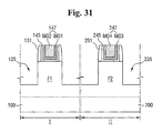
Referring to FIGS. 31 and 32 , a first distance L1/L3 between a first gate electrode 147 (or center of the channel region) and a first recess 125 is substantially equal to a second distance L2/L4 between a second gate electrode 247 (or center of the channel region) and a second recess 225, unlike in FIGS. 24 through 26 .
Referring to FIG. 32 , a third mask 480 which exposes a first region I but does not expose a second region II is formed. An epitaxial process is performed while the first recess 125 is in-situ doped with impurities to a first impurity concentration. As a result, a first source/drain 161 is formed. Then, the third mask 480 is removed.
Referring to FIG. 6 , a fourth mask which exposes the second region II but does not expose the first region I is formed. An epitaxial process is performed while the second recess 225 is in-situ doped with impurities to a second impurity concentration. As a result, a second source/drain 261 is formed.
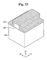
Hereinafter, methods of forming a fin usable in methods of fabricating semiconductor device according to some embodiments of the present inventive concept will be described with reference to FIGS. 33 through 35 . The methods in FIGS. 33 through 35 may be methods of forming a plurality of fins illustrated in FIG. 12 . The methods may include, for example, a SIT process. In FIGS. 33 through 35 , methods of forming two fins are illustrated as an example. However, the present inventive concept is not limited to this example.
Referring to FIG. 33 , a sacrificial pattern 501 is formed on a substrate 100. Then, a mask layer 505 is formed on the substrate 100 having the sacrificial pattern 501. The mask layer 505 may be conformally formed along a top surface of the substrate 100 having the sacrificial pattern 501. The sacrificial pattern 501 and the mask layer 505 may be made of materials that have an etch selectivity with respect to each other. For example, the mask layer 505 may include at least one of silicon oxide, silicon nitride, silicon oxynitride, photoresist, spin on glass (SOG) and spin on hard mask (SOH), and the sacrificial pattern 501 may be made of one of the above materials which is different from the material of the mask layer 505.
The sacrificial pattern 501 and the mask layer 505 may be formed by at least one of a physical vapor deposition (PVD) process, a chemical vapor deposition (CVD) process, an atomic layer deposition (ALD) process, and a spin coating process.
Referring to FIG. 34 , spacer-shaped mask patterns 506 are respectively formed on side walls of the sacrificial pattern 501 using an etch-back process. Then, the sacrificial pattern 501 is removed. The mask patterns 506 may have substantially the same width. A trench 511 may be formed between the mask patterns 506.
Referring to FIG. 35 , the substrate 100 is etched using the mask patterns 506 as an etch mask. As a result, fins F11 and F22 having a predetermined width may be formed. A trench 512 may be formed between the adjacent fins F11 and F12 by an etching process. In the etching process, upper parts of the mask patterns 506 may also be etched. Thus, the upper parts of the mask patterns 506 may become round.
The mask patterns 506 may be removed, thereby completing the fins F11 and F12 which are separated from each other and have the predetermined width.
Referring to FIG. 36 , the electronic system 1100 according to an embodiment of the present inventive concept may include a controller 1110, an input/output (I/O) device 1120, a memory device 1130, an interface 1140, and a bus 1150. The controller 1110, the I/O device 1120, the memory device 1130, and/or the interface 1140 may be coupled to each other through the bus 1150. The bus 1150 corresponds to a path through which data is transferred.
The controller 1110 may include at least one of a microprocessor, a digital signal processor, a microcontroller, or logic elements capable of performing similar functions to those of the above elements. The I/O device 1120 may include a keypad, a keyboard, and a display device. The memory device 1130 may store data and/or commands. The interface 1140 may transmit data to a communication network or receive data from the communication network. The interface 1140 can transmit data over a wire or wirelessly. For example, the interface 1140 may be an antenna or a wireless transceiver. The electronic system 1100 may further include a high-speed DRAM and/or a high-speed SRAM as an operation memory for improving the operation of the controller 1110. A fin field effect transistor according to embodiments of the present inventive concept may be provided within the memory device 1130 or provided as a part of the controller 1110 or the I/O device 1120.
The electronic system 1100 can be applied to a personal digital assistant (PDA), a portable computer, a web tablet, a wireless phone, a mobile phone, a digital music player, a memory card, and all electronic products that can transmit and/or receive information wirelessly.
In concluding the detailed description, those skilled in the art will appreciate that many variations and modifications can be made to the embodiments without substantially departing from the principles of the present invention. Therefore, the disclosed embodiments of the invention are used in a generic and descriptive sense only and not for purposes of limitation.
Claims (37)
1. An integrated circuit comprising:
first and second fin field effect transistors (finFETs) of same particular conductivity type on a substrate, wherein a first source/drain of the first finFET that includes electrically active impurities of a first conductivity type throughout the first source/drain is closer to a first gate electrode of the first finFET than a second source/drain of the second finFET that includes electrically active impurities of the same first conductivity type throughout the second source/drain is to a second gate electrode of the second finFET,
wherein a first channel region of the first finFET and a second channel region of the second finFET comprise respective fins that extend from the substrate to protrude from a device isolation layer to provide upper side walls and a top surface of the respective fins positioned between the first and second source/drains, respectively,
wherein the first gate electrode of the first finFET and the second gate electrode of the second finFET each wrap around three sides of the respective one of the first and second channel regions.
2. The circuit of claim 1 wherein a first interface of the first source/drain and the first channel region is closer to the first gate electrode than a second interface of the second source/drain and the second channel region is to the second gate electrode.
3. The circuit of claim 1 wherein the first and second source/drains comprise a particular lattice constant, and wherein the first source/drain applies greater stress to the first channel region than the second source/drain applies to the second channel region.
4. The circuit of claim 3 wherein the first source/drain extends past an outermost lower corner of a gate structure of the first finFET into the first channel region to define an undercut region beneath the first finFET; and
wherein the second source/drain is aligned to a gate structure of the second finFET.
5. The circuit of claim 1 wherein the first and second source/drains comprise first and second raised source/drains, respectively, wherein the first source/drain extends past an outermost lower corner of a gate structure of the first finFET into the first channel region to define a first undercut region beneath the first finFET; and
wherein the second source/drain extends past an outermost lower corner of a gate structure of the second finFET into the second channel region to define a second undercut region beneath the second finFET.
6. The circuit of claim 1 wherein the first and second source/drains comprise different lattice constants than the first and second channel regions.
7. The circuit of claim 1 wherein the first and second source/drains comprise first and second raised source/drains, respectively, wherein the first raised source/drain wraps around an outermost lower corner of a gate structure of the first finFET into the first channel region to define an undercut region beneath the first finFET; and
wherein the second source/drain is formed aligned to a gate structure of the second finFET.
8. The circuit of claim 1 wherein the first and second source/drains comprise first and second raised source/drains, respectively, wherein the first raised source/drain wraps around an outermost lower corner of a gate structure of the first finFET into the first channel region to define a first undercut region beneath the first finFET; and
wherein the second raised source/drain wraps around an outermost lower corner of a gate structure of the second finFET into the second channel region to define a second undercut region beneath the second finFET.
9. The circuit of claim 1 further comprising:
a first spacer including an outer side wall of a gate structure of the first finFET to provide a first thickness; and
a second spacer including an outer side wall of a gate structure of the second finFET to provide a second thickness that is greater than the first thickness.
10. The circuit of claim 9 wherein the first source/drain is formed self-aligned to the first spacer and the second source/drain is formed self-aligned to the second spacer.
11. The circuit of claim 9 wherein a number of layers included in the first spacer is less than a number of layers included in the second spacer.
12. The circuit of claim 11 wherein the first source/drain is formed self-aligned to the first spacer and the second source/drain is formed self-aligned to the second spacer.
13. The circuit of claim 1 wherein the first and second finFETs comprise PMOS finFETs, the first and second channel regions include a first material comprising a first lattice constant and the first and second source/drains include a second material comprising a second lattice constant that is greater than the first lattice constant.
14. The circuit of claim 13 wherein the first material comprises Si and the second material comprises SiGe.
15. The circuit of claim 1 wherein the first and second finFETs comprise NMOS finFETs, the channel regions include a first material comprising a first lattice constant and the source/drains of the first and second finFETs include a second material comprising a second lattice constant that is less than the first lattice constant.
16. The circuit of claim 15 wherein the first material comprises Si and the second material comprises SiC.
17. The circuit of claim 1 wherein at least one of the respective fins comprises a width measured between the upper side walls of about 20 nm or less.
18. The circuit of claim 17 wherein the at least one of the respective fins comprises a side wall image transfer fin.
19. The circuit of claim 1 ,
wherein the first and second gate electrodes each includes a first conductive gate layer in an outer portion of the respective gate electrode and a second conductive gate layer in an inner portion of the respective gate electrode in a recess defined by the first conductive gate layer.
20. The circuit of claim 19 wherein the first and second conductive gate layers comprise first and second metal layers, respectively.
21. The circuit of claim 19 wherein the first metal layers comprise TiN, TaN, TiC, TaC, Si, or SiGe and the second metal layers comprise W and/or Al.
22. The circuit of claim 1 wherein the substrate comprises a bulk silicon or a silicon-on-insulator substrate.
23. An integrated circuit comprising:
a substrate;
a first fin field effect transistor (finFET) of a particular conductivity type on the substrate, including a first gate structure, a first source/drain that includes electrically active impurities of a first conductivity type throughout the first source/drain, and a first channel region, wherein a first interface between the first source/drain and the first channel region is aligned to the first gate structure a first distance from a first gate electrode of the first finFET, and wherein the first gate structure wraps around three sides of the first channel region; and
a second finFET of the particular conductivity type on the substrate, including a second gate structure, a second source/drain that includes electrically active impurities of the same first conductivity type throughout the second source/drain, and a second channel region, wherein the second source/drain wraps around a lower outer corner of the second gate structure to form a second interface between the second source/drain and the second channel region a second distance from a second gate electrode of the second finFET that is less than the first distance, and wherein the second gate structure wraps around three sides of the second channel region,
wherein the first and second channel regions comprise respective fins that extend from the substrate to protrude from a device isolation layer to provide upper side walls and a top surface of the respective fins positioned between the first and second source/drains, respectively,
wherein the particular conductivity type of the second finFET is the same as the particular conductivity type of the first finFET.
24. The circuit of claim 23 wherein the first and second finFETs comprise PMOS finFETs, the first and second channel regions include a first material comprising a first lattice constant and the first and second source/drains include a second material comprising a second lattice constant that is greater than the first lattice constant.
25. The circuit of claim 24 wherein the first material comprises Si and the second material comprises SiGe.
26. The circuit of claim 23 wherein the first and second finFETs comprise NMOS finFETs, the first and second channel regions include a first material comprising a first lattice constant and the first and second source/drains include a second material comprising a second lattice constant that is less than the first lattice constant.
27. The circuit of claim 26 wherein the first material comprises Si and the second material comprises SiC.
28. The circuit of claim 23 wherein the first and second gate electrodes each include a first conductive gate layer in an outer portion of the respective gate electrode and a second conductive gate layer in an inner portion of the respective gate electrode in a recess defined by the first conductive gate layer.
29. The circuit of claim 28 wherein the first and second conductive gate layers comprise first and second metal layers, respectively.
30. The circuit of claim 29 wherein the first metal layers comprise TiN, TaN, TiC, TaC, Si, or SiGe and the second metal layers comprise W and/or Al.
31. The circuit of claim 23 wherein the substrate comprises a bulk silicon or a silicon-on-insulator substrate.
32. The circuit of claim 23 wherein the first and second source/drains comprise different lattice constants than the first and second channel regions.
33. An integrated circuit comprising:
a substrate;
a first fin field effect transistor (finFET) of a particular conductivity type on the substrate, including a first gate structure, a first source/drain that includes electrically active impurities of a first conductivity type, and a first channel region, wherein the first source/drain wraps around a lower outer corner of the first gate structure to form a first interface between the first source/drain and the first channel region a first distance from a first gate electrode of the first finFET, and wherein the first gate structure wraps around three sides of the first channel region; and
a second finFET of the particular conductivity type on the substrate, including a second gate structure, a second source/drain that includes electrically active impurities of the same first conductivity type, and a second channel region, wherein the second source/drain wraps around a lower outer corner of the second gate structure to form a second interface between the second source/drain and the second channel region a second distance from a second gate electrode of the second finFET that is less than the first distance, so that the second source/drain applies greater stress to the second channel region than the first source/drain applies to the first channel region, and wherein the second gate structure wraps around three sides of the second channel region,
wherein the first and second channel regions comprise respective fins that extend from the substrate to protrude from a device isolation layer to provide upper side walls and a top surface of the respective fins positioned between the first and second source/drains, respectively, and
wherein the particular conductivity type of the second finFET is the same as the particular conductivity type of the first finFET.
34. The circuit of claim 33 wherein the first and second source/drains comprise different lattice constants than the first and second channel regions, the circuit further comprising:
a first stress film on the first finFET; and
a second stress film on the second finFET,
wherein the first stress film applies stress to the first finFET, and
wherein the second stress film applies stress to the second finFET.
35. The circuit of claim 33 wherein the first and second source/drains comprise different lattice constants than the first and second channel regions.
36. An integrated circuit comprising:
a first fin field effect transistors (finFET) of a particular conductivity type included in a logic region of a substrate; and
a second finFET, of the particular conductivity type, in a Static Random Access Memory region of the substrate, wherein a first source/drain that includes electrically active impurities of a first conductivity type of the first finFET is spaced apart from a first gate electrode of the first finFET differently than a second source/drain that includes electrically active impurities of the same first conductivity type of the second finFET is spaced apart from a second gate electrode of the second finFET,
wherein a first channel region of the first finFET and a second channel region of the second finFET comprise respective fins that extend from the substrate to protrude from a device isolation layer to provide upper side walls and a top surface of the respective fins positioned between the first and second source/drains, respectively,
wherein the particular conductivity type of the second finFET is the same as the particular conductivity type of the first finFET,
wherein the first gate electrode of the first finFET and the second gate electrode of the second finFET each wrap around three sides of the respective one of the first and second channel regions.
37. The circuit of claim 36 wherein a first interface between the first source/drain and the first channel region and a second interface between the second source/drain and the second channel region are separated from the first and second gate electrodes differently.
Applications Claiming Priority (2)
| Application Number | Priority Date | Filing Date | Title |
|---|---|---|---|
| KR10-2012-0043279 | 2012-04-25 | ||
| KR1020120043279A KR101912582B1 (en) | 2012-04-25 | 2012-04-25 | Semiconductor device and fabricated method thereof |
Publications (2)
| Publication Number | Publication Date |
|---|---|
| US20130285143A1 US20130285143A1 (en) | 2013-10-31 |
| US9490177B2 true US9490177B2 (en) | 2016-11-08 |
Family
ID=49323359
Family Applications (1)
| Application Number | Title | Priority Date | Filing Date |
|---|---|---|---|
| US13/617,582 Active 2033-08-01 US9490177B2 (en) | 2012-04-25 | 2012-09-14 | Integrated circuit devices including stress proximity effects and methods of fabricating the same |
Country Status (6)
| Country | Link |
|---|---|
| US (1) | US9490177B2 (en) |
| JP (1) | JP6347576B2 (en) |
| KR (1) | KR101912582B1 (en) |
| CN (1) | CN103378098B (en) |
| DE (1) | DE102013103798A1 (en) |
| TW (1) | TWI615945B (en) |
Cited By (6)
| Publication number | Priority date | Publication date | Assignee | Title |
|---|---|---|---|---|
| US20170278865A1 (en) * | 2015-10-16 | 2017-09-28 | Taiwan Semiconductor Manufacturing Company, Ltd. | Method of tuning source/drain proximity for input/output device reliability enhancement |
| US9923094B2 (en) | 2015-03-13 | 2018-03-20 | Taiwan Semiconductor Manufacturing Company, Ltd. | Source/drain regions for fin field effect transistors and methods of forming same |
| US9947664B1 (en) * | 2016-10-14 | 2018-04-17 | International Business Machines Corporation | Semiconductor device and method of forming the semiconductor device |
| US10546946B2 (en) | 2016-02-24 | 2020-01-28 | Renesas Electronics Corporation | Method for manufacturing semiconductor device having thinned fins |
| US11205647B2 (en) | 2019-06-28 | 2021-12-21 | Taiwan Semiconductor Manufacturing Company, Ltd. | Semiconductor device and method of manufacture |
| US11532723B2 (en) | 2019-10-29 | 2022-12-20 | Taiwan Semiconductor Manufacturing Company, Ltd. | Fin-end gate structures and method forming same |
Families Citing this family (46)
| Publication number | Priority date | Publication date | Assignee | Title |
|---|---|---|---|---|
| KR20140099743A (en) * | 2013-02-04 | 2014-08-13 | 삼성전자주식회사 | Semiconductor device and method for fabricating the same |
| KR20140106270A (en) * | 2013-02-26 | 2014-09-03 | 삼성전자주식회사 | Integrated circuit devices and fabricated method thereof |
| US9793268B2 (en) * | 2014-01-24 | 2017-10-17 | Taiwan Semiconductor Manufacturing Company, Ltd. | Method and structure for gap filling improvement |
| KR102193493B1 (en) * | 2014-02-03 | 2020-12-21 | 삼성전자주식회사 | Semiconductor devices and methods of manufacturing the same |
| US9269626B2 (en) * | 2014-02-06 | 2016-02-23 | Taiwan Semiconductor Manufacturing Co., Ltd. | Integrated circuit structure and method for manufacturing thereof |
| US9553171B2 (en) * | 2014-02-14 | 2017-01-24 | Taiwan Semiconductor Manufacturing Co., Ltd. | Fin field effect transistor (FinFET) device and method for forming the same |
| KR20230003606A (en) | 2014-03-24 | 2023-01-06 | 인텔 코포레이션 | Techniques for achieving multiple transistor fin dimensions on a single die |
| KR102017611B1 (en) * | 2014-04-04 | 2019-09-04 | 삼성전자주식회사 | Semiconductor device and method of manufacturing the same |
| US9466669B2 (en) * | 2014-05-05 | 2016-10-11 | Samsung Electronics Co., Ltd. | Multiple channel length finFETs with same physical gate length |
| KR102158962B1 (en) | 2014-05-08 | 2020-09-24 | 삼성전자 주식회사 | Semiconductor device and method for fabricating the same |
| KR102200345B1 (en) * | 2014-06-26 | 2021-01-11 | 삼성전자주식회사 | Semiconductor device and method of manufacturing the same |
| KR102231208B1 (en) * | 2014-07-21 | 2021-03-24 | 삼성전자주식회사 | Method of manufacturing semiconductor device |
| US9893191B2 (en) | 2014-08-20 | 2018-02-13 | Taiwan Semiconductor Manufacturing Company, Ltd. | FinFET transistor with u-shaped channel |
| KR102227128B1 (en) | 2014-09-03 | 2021-03-12 | 삼성전자주식회사 | Semiconductor device and method for fabricating the same |
| CN105470286B (en) * | 2014-09-12 | 2018-09-18 | 中国科学院微电子研究所 | Semiconductor devices and its manufacturing method |
| US9691471B2 (en) * | 2014-09-15 | 2017-06-27 | Taiwan Semiconductor Manufacturing Company, Ltd. | SRAM cells with vertical gate-all-round MOSFETs |
| KR102265956B1 (en) | 2014-09-29 | 2021-06-17 | 삼성전자주식회사 | Semiconductor devices having a source/drain and Method for fabricating the same |
| US9558946B2 (en) | 2014-10-03 | 2017-01-31 | Taiwan Semiconductor Manufacturing Company, Ltd. | FinFETs and methods of forming FinFETs |
| US9735256B2 (en) * | 2014-10-17 | 2017-08-15 | Taiwan Semiconductor Manufacturing Company, Ltd. | Method and structure for FinFET comprising patterned oxide and dielectric layer under spacer features |
| US20160190318A1 (en) * | 2014-12-30 | 2016-06-30 | Taiwan Semiconductor Manufacturing Co., Ltd. | Semiconductor device and manufacturing method thereof |
| US9564528B2 (en) * | 2015-01-15 | 2017-02-07 | Taiwan Semiconductor Manufacturing Co., Ltd. | Semiconductor device and manufacturing method thereof |
| KR102269415B1 (en) * | 2015-03-16 | 2021-06-24 | 삼성전자주식회사 | Semiconductor device |
| US9537007B2 (en) | 2015-04-07 | 2017-01-03 | Qualcomm Incorporated | FinFET with cut gate stressor |
| KR102339777B1 (en) * | 2015-04-14 | 2021-12-15 | 삼성전자주식회사 | Semiconductor device |
| KR102290538B1 (en) | 2015-04-16 | 2021-08-19 | 삼성전자주식회사 | Semiconductor device and method for manufacturing the same |
| KR102376481B1 (en) * | 2015-05-22 | 2022-03-21 | 삼성전자주식회사 | Semiconductor devices including field effect transistors and method of fabricating the same |
| KR102374108B1 (en) * | 2015-06-02 | 2022-03-14 | 삼성전자주식회사 | Semiconductor device having stressor and method of fabricating the same |
| US9418897B1 (en) | 2015-06-15 | 2016-08-16 | Taiwan Semiconductor Manufacturing Company, Ltd. | Wrap around silicide for FinFETs |
| US9679978B2 (en) | 2015-09-24 | 2017-06-13 | Samsung Electronics Co., Ltd. | Semiconductor device and method for fabricating the same |
| US10121879B2 (en) | 2015-09-28 | 2018-11-06 | International Business Machines Corporation | Forming odd number of fins by sidewall imaging transfer |
| US9722079B2 (en) | 2015-10-15 | 2017-08-01 | Taiwan Semiconductor Manufacturing Co., Ltd. | Fin-type field effect transistor structure and manufacturing method thereof |
| US9960273B2 (en) * | 2015-11-16 | 2018-05-01 | Taiwan Semiconductor Manufacturing Company, Ltd. | Integrated circuit structure with substrate isolation and un-doped channel |
| TWI680502B (en) * | 2016-02-03 | 2019-12-21 | 聯華電子股份有限公司 | Semiconductor device and method of manufacturing the same |
| TWI612674B (en) * | 2016-03-24 | 2018-01-21 | 台灣積體電路製造股份有限公司 | Finfet and the methods of fabricating the same |
| US9748389B1 (en) | 2016-03-25 | 2017-08-29 | Taiwan Semiconductor Manufacturing Co., Ltd. | Method for semiconductor device fabrication with improved source drain epitaxy |
| KR102452999B1 (en) * | 2016-05-03 | 2022-10-07 | 삼성전자주식회사 | Semiconductor device and method for fabricating the same |
| US9905645B2 (en) * | 2016-05-24 | 2018-02-27 | Samsung Electronics Co., Ltd. | Vertical field effect transistor having an elongated channel |
| US9985042B2 (en) * | 2016-05-24 | 2018-05-29 | Silicon Storage Technology, Inc. | Method of integrating FinFET CMOS devices with embedded nonvolatile memory cells |
| CN106443410B (en) * | 2016-08-30 | 2019-05-03 | 广西南宁市沃威机电设备有限公司 | A kind of IC testing method |
| US10229921B2 (en) * | 2017-02-03 | 2019-03-12 | International Business Machines Corporation | Structure featuring ferroelectric capacitance in interconnect level for steep sub-threshold complementary metal oxide semiconductor transistors |
| US10367086B2 (en) * | 2017-06-14 | 2019-07-30 | Hrl Laboratories, Llc | Lateral fin static induction transistor |
| KR102360410B1 (en) * | 2017-08-30 | 2022-02-08 | 삼성전자주식회사 | Semiconductor device |
| CN109585534B (en) * | 2017-09-29 | 2022-03-22 | 中芯国际集成电路制造(上海)有限公司 | Semiconductor device and method of forming the same |
| US10879125B2 (en) | 2018-12-27 | 2020-12-29 | Nanya Technology Corporation | FinFET structure and method of manufacturing the same |
| US11164816B2 (en) | 2019-09-05 | 2021-11-02 | Nanya Technology Corporation | Semiconductor device and method for fabricating the same |
| US11610979B2 (en) * | 2020-08-13 | 2023-03-21 | Taiwan Semiconductor Manufacturing Co., Ltd. | Profile control in forming epitaxy regions for transistors |
Citations (9)
| Publication number | Priority date | Publication date | Assignee | Title |
|---|---|---|---|---|
| US20060043616A1 (en) * | 2004-08-30 | 2006-03-02 | International Business Machines Corporation | Finfet with low gate capacitance and low extrinsic resistance |
| US20070045729A1 (en) * | 2005-08-31 | 2007-03-01 | Jan Hoentschel | Technique for forming recessed strained drain/source regions in nmos and pmos transistors |
| US20090032880A1 (en) | 2007-08-03 | 2009-02-05 | Applied Materials, Inc. | Method and apparatus for tunable isotropic recess etching of silicon materials |
| US7939413B2 (en) | 2005-12-08 | 2011-05-10 | Samsung Electronics Co., Ltd. | Embedded stressor structure and process |
| US20110210402A1 (en) * | 2008-08-12 | 2011-09-01 | International Business Machines Corporation | Metal-gate high-k reference structure |
| US20110269287A1 (en) * | 2010-04-28 | 2011-11-03 | Taiwan Semiconductor Manufacturing Company, Ltd. | Methods for doping fin field-effect transistors |
| US20110291201A1 (en) * | 2010-05-26 | 2011-12-01 | Taiwan Semiconductor Manufacturing Company, Ltd. | Multi-strained source/drain structures |
| US20120001238A1 (en) * | 2010-06-30 | 2012-01-05 | Taiwan Semiconductor Manufacturing Company, Ltd. | Integrated circuit device with well controlled surface proximity and method of manufacturing same |
| US20120313178A1 (en) * | 2011-06-13 | 2012-12-13 | Po-Jui Liao | Semiconductor device having metal gate and manufacturing method thereof |
Family Cites Families (13)
| Publication number | Priority date | Publication date | Assignee | Title |
|---|---|---|---|---|
| JP4530552B2 (en) * | 2001-01-29 | 2010-08-25 | 富士通セミコンダクター株式会社 | Semiconductor device and manufacturing method thereof |
| AU2002368388A1 (en) * | 2002-11-25 | 2004-06-18 | International Business Machines Corporation | Strained finfet cmos device structures |
| KR100583731B1 (en) * | 2004-08-03 | 2006-05-26 | 삼성전자주식회사 | Nor type memory device and method of fabricating the same |
| JP2006108602A (en) * | 2004-09-10 | 2006-04-20 | Toshiba Corp | Semiconductor device and its manufacturing method |
| JP2006253317A (en) * | 2005-03-09 | 2006-09-21 | Fujitsu Ltd | SEMICONDUCTOR INTEGRATED CIRCUIT DEVICE AND p-CHANNEL MOS TRANSISTOR |
| US7238990B2 (en) * | 2005-04-06 | 2007-07-03 | Freescale Semiconductor, Inc. | Interlayer dielectric under stress for an integrated circuit |
| US7525160B2 (en) * | 2005-12-27 | 2009-04-28 | Intel Corporation | Multigate device with recessed strain regions |
| US7776695B2 (en) * | 2006-01-09 | 2010-08-17 | International Business Machines Corporation | Semiconductor device structure having low and high performance devices of same conductive type on same substrate |
| JP2007207837A (en) * | 2006-01-31 | 2007-08-16 | Toshiba Corp | Semiconductor device, and method of manufacturing same |
| JP5206668B2 (en) * | 2007-03-28 | 2013-06-12 | 富士通セミコンダクター株式会社 | Manufacturing method of semiconductor device |
| US7829951B2 (en) * | 2008-11-06 | 2010-11-09 | Qualcomm Incorporated | Method of fabricating a fin field effect transistor (FinFET) device |
| US8362575B2 (en) * | 2009-09-29 | 2013-01-29 | Taiwan Semiconductor Manufacturing Company, Ltd. | Controlling the shape of source/drain regions in FinFETs |
| KR101707816B1 (en) | 2010-10-26 | 2017-02-20 | 에스케이이노베이션 주식회사 | Thermoelectric Generation Vehicle, TEGV |
-
2012
- 2012-04-25 KR KR1020120043279A patent/KR101912582B1/en active IP Right Grant
- 2012-09-14 US US13/617,582 patent/US9490177B2/en active Active
-
2013
- 2013-03-08 TW TW102108289A patent/TWI615945B/en active
- 2013-04-09 JP JP2013081451A patent/JP6347576B2/en active Active
- 2013-04-16 DE DE102013103798A patent/DE102013103798A1/en active Pending
- 2013-04-22 CN CN201310140963.7A patent/CN103378098B/en active Active
Patent Citations (9)
| Publication number | Priority date | Publication date | Assignee | Title |
|---|---|---|---|---|
| US20060043616A1 (en) * | 2004-08-30 | 2006-03-02 | International Business Machines Corporation | Finfet with low gate capacitance and low extrinsic resistance |
| US20070045729A1 (en) * | 2005-08-31 | 2007-03-01 | Jan Hoentschel | Technique for forming recessed strained drain/source regions in nmos and pmos transistors |
| US7939413B2 (en) | 2005-12-08 | 2011-05-10 | Samsung Electronics Co., Ltd. | Embedded stressor structure and process |
| US20090032880A1 (en) | 2007-08-03 | 2009-02-05 | Applied Materials, Inc. | Method and apparatus for tunable isotropic recess etching of silicon materials |
| US20110210402A1 (en) * | 2008-08-12 | 2011-09-01 | International Business Machines Corporation | Metal-gate high-k reference structure |
| US20110269287A1 (en) * | 2010-04-28 | 2011-11-03 | Taiwan Semiconductor Manufacturing Company, Ltd. | Methods for doping fin field-effect transistors |
| US20110291201A1 (en) * | 2010-05-26 | 2011-12-01 | Taiwan Semiconductor Manufacturing Company, Ltd. | Multi-strained source/drain structures |
| US20120001238A1 (en) * | 2010-06-30 | 2012-01-05 | Taiwan Semiconductor Manufacturing Company, Ltd. | Integrated circuit device with well controlled surface proximity and method of manufacturing same |
| US20120313178A1 (en) * | 2011-06-13 | 2012-12-13 | Po-Jui Liao | Semiconductor device having metal gate and manufacturing method thereof |
Cited By (12)
| Publication number | Priority date | Publication date | Assignee | Title |
|---|---|---|---|---|
| US9923094B2 (en) | 2015-03-13 | 2018-03-20 | Taiwan Semiconductor Manufacturing Company, Ltd. | Source/drain regions for fin field effect transistors and methods of forming same |
| US20170278865A1 (en) * | 2015-10-16 | 2017-09-28 | Taiwan Semiconductor Manufacturing Company, Ltd. | Method of tuning source/drain proximity for input/output device reliability enhancement |
| US10074668B2 (en) * | 2015-10-16 | 2018-09-11 | Taiwan Semiconductor Manfacturing Company, Ltd. | Input/output (I/O) devices with greater source/drain proximity than non-I/O devices |
| US10546946B2 (en) | 2016-02-24 | 2020-01-28 | Renesas Electronics Corporation | Method for manufacturing semiconductor device having thinned fins |
| US11217682B2 (en) | 2016-02-24 | 2022-01-04 | Renesas Electronics Corporation | Method for manufacturing semiconductor device having thinned fins |
| US9947664B1 (en) * | 2016-10-14 | 2018-04-17 | International Business Machines Corporation | Semiconductor device and method of forming the semiconductor device |
| US20180108659A1 (en) * | 2016-10-14 | 2018-04-19 | International Business Machines Corporation | Semiconductor device and method of forming the semiconductor device |
| US20180122807A1 (en) * | 2016-10-14 | 2018-05-03 | International Business Machines Corporation | Semiconductor device and method of forming the semiconductor device |
| US10607992B2 (en) * | 2016-10-14 | 2020-03-31 | International Business Machines Corporation | Semiconductor device and method of forming the semiconductor device |
| US10978454B2 (en) * | 2016-10-14 | 2021-04-13 | Elpis Technologies Inc. | Semiconductor device and method of forming the semiconductor device |
| US11205647B2 (en) | 2019-06-28 | 2021-12-21 | Taiwan Semiconductor Manufacturing Company, Ltd. | Semiconductor device and method of manufacture |
| US11532723B2 (en) | 2019-10-29 | 2022-12-20 | Taiwan Semiconductor Manufacturing Company, Ltd. | Fin-end gate structures and method forming same |
Also Published As
| Publication number | Publication date |
|---|---|
| CN103378098B (en) | 2018-09-14 |
| DE102013103798A1 (en) | 2013-10-31 |
| TWI615945B (en) | 2018-02-21 |
| TW201344886A (en) | 2013-11-01 |
| KR101912582B1 (en) | 2018-12-28 |
| JP6347576B2 (en) | 2018-06-27 |
| US20130285143A1 (en) | 2013-10-31 |
| KR20130120201A (en) | 2013-11-04 |
| JP2013229597A (en) | 2013-11-07 |
| CN103378098A (en) | 2013-10-30 |
Similar Documents
| Publication | Publication Date | Title |
|---|---|---|
| US9490177B2 (en) | Integrated circuit devices including stress proximity effects and methods of fabricating the same | |
| US9153692B2 (en) | Semiconductor device having a stress film on a side surface of a fin | |
| US9673099B2 (en) | Method of fabricating integrated circuit devices | |
| US10840142B2 (en) | Semiconductor device including a three-dimensional channel | |
| TWI573222B (en) | Semiconductor device and fabricating method thereof | |
| TWI692813B (en) | Method of fabricating semiconductor device | |
| US9299811B2 (en) | Methods of fabricating semiconductor devices | |
| US9923058B2 (en) | Semiconductor device having a fin | |
| US9461148B2 (en) | Semiconductor device and method of fabricating the same | |
| US9525036B2 (en) | Semiconductor device having gate electrode with spacers on fin structure and silicide layer filling the recess | |
| US20130249003A1 (en) | Field effect transistors including fin structures with different doped regions and semiconductor devices including the same | |
| US9520297B2 (en) | Semiconductor device and method of fabricating the same | |
| US9773869B2 (en) | Semiconductor device and method of fabricating the same | |
| US20140346617A1 (en) | Semiconductor device and method for fabricating the same | |
| US20140203335A1 (en) | Semiconductor Devices and Methods for Fabricating the Same |
Legal Events
| Date | Code | Title | Description |
|---|---|---|---|
| AS | Assignment |
Owner name: SAMSUNG ELECTRONICS CO., LTD., KOREA, REPUBLIC OF Free format text: ASSIGNMENT OF ASSIGNORS INTEREST;ASSIGNORS:OH, CHANG-WOO;KANG, MYUNG-GIL;JUNG, YOUNG-CHAI;REEL/FRAME:028975/0627 Effective date: 20120802 |
|
| STCF | Information on status: patent grant |
Free format text: PATENTED CASE |
|
| MAFP | Maintenance fee payment |
Free format text: PAYMENT OF MAINTENANCE FEE, 4TH YEAR, LARGE ENTITY (ORIGINAL EVENT CODE: M1551); ENTITY STATUS OF PATENT OWNER: LARGE ENTITY Year of fee payment: 4 |