US9489256B2 - Device quality metrics using unsatisfied parity checks - Google Patents
Device quality metrics using unsatisfied parity checks Download PDFInfo
- Publication number
- US9489256B2 US9489256B2 US14/101,679 US201314101679A US9489256B2 US 9489256 B2 US9489256 B2 US 9489256B2 US 201314101679 A US201314101679 A US 201314101679A US 9489256 B2 US9489256 B2 US 9489256B2
- Authority
- US
- United States
- Prior art keywords
- codeword
- bit error
- circuit
- error rate
- decoding procedure
- Prior art date
- Legal status (The legal status is an assumption and is not a legal conclusion. Google has not performed a legal analysis and makes no representation as to the accuracy of the status listed.)
- Active, expires
Links
Images


Classifications
-
- G—PHYSICS
- G06—COMPUTING; CALCULATING OR COUNTING
- G06F—ELECTRIC DIGITAL DATA PROCESSING
- G06F11/00—Error detection; Error correction; Monitoring
- G06F11/07—Responding to the occurrence of a fault, e.g. fault tolerance
- G06F11/0703—Error or fault processing not based on redundancy, i.e. by taking additional measures to deal with the error or fault not making use of redundancy in operation, in hardware, or in data representation
- G06F11/0751—Error or fault detection not based on redundancy
- G06F11/0754—Error or fault detection not based on redundancy by exceeding limits
- G06F11/076—Error or fault detection not based on redundancy by exceeding limits by exceeding a count or rate limit, e.g. word- or bit count limit
-
- G—PHYSICS
- G06—COMPUTING; CALCULATING OR COUNTING
- G06F—ELECTRIC DIGITAL DATA PROCESSING
- G06F11/00—Error detection; Error correction; Monitoring
- G06F11/07—Responding to the occurrence of a fault, e.g. fault tolerance
- G06F11/08—Error detection or correction by redundancy in data representation, e.g. by using checking codes
- G06F11/10—Adding special bits or symbols to the coded information, e.g. parity check, casting out 9's or 11's
- G06F11/1008—Adding special bits or symbols to the coded information, e.g. parity check, casting out 9's or 11's in individual solid state devices
- G06F11/1068—Adding special bits or symbols to the coded information, e.g. parity check, casting out 9's or 11's in individual solid state devices in sector programmable memories, e.g. flash disk
-
- G—PHYSICS
- G06—COMPUTING; CALCULATING OR COUNTING
- G06F—ELECTRIC DIGITAL DATA PROCESSING
- G06F11/00—Error detection; Error correction; Monitoring
- G06F11/07—Responding to the occurrence of a fault, e.g. fault tolerance
- G06F11/0703—Error or fault processing not based on redundancy, i.e. by taking additional measures to deal with the error or fault not making use of redundancy in operation, in hardware, or in data representation
- G06F11/0706—Error or fault processing not based on redundancy, i.e. by taking additional measures to deal with the error or fault not making use of redundancy in operation, in hardware, or in data representation the processing taking place on a specific hardware platform or in a specific software environment
- G06F11/0727—Error or fault processing not based on redundancy, i.e. by taking additional measures to deal with the error or fault not making use of redundancy in operation, in hardware, or in data representation the processing taking place on a specific hardware platform or in a specific software environment in a storage system, e.g. in a DASD or network based storage system
-
- G—PHYSICS
- G06—COMPUTING; CALCULATING OR COUNTING
- G06F—ELECTRIC DIGITAL DATA PROCESSING
- G06F11/00—Error detection; Error correction; Monitoring
- G06F11/07—Responding to the occurrence of a fault, e.g. fault tolerance
- G06F11/0703—Error or fault processing not based on redundancy, i.e. by taking additional measures to deal with the error or fault not making use of redundancy in operation, in hardware, or in data representation
- G06F11/079—Root cause analysis, i.e. error or fault diagnosis
-
- G—PHYSICS
- G11—INFORMATION STORAGE
- G11B—INFORMATION STORAGE BASED ON RELATIVE MOVEMENT BETWEEN RECORD CARRIER AND TRANSDUCER
- G11B20/00—Signal processing not specific to the method of recording or reproducing; Circuits therefor
- G11B20/10—Digital recording or reproducing
- G11B20/18—Error detection or correction; Testing, e.g. of drop-outs
- G11B20/1833—Error detection or correction; Testing, e.g. of drop-outs by adding special lists or symbols to the coded information
-
- H—ELECTRICITY
- H03—ELECTRONIC CIRCUITRY
- H03M—CODING; DECODING; CODE CONVERSION IN GENERAL
- H03M13/00—Coding, decoding or code conversion, for error detection or error correction; Coding theory basic assumptions; Coding bounds; Error probability evaluation methods; Channel models; Simulation or testing of codes
- H03M13/61—Aspects and characteristics of methods and arrangements for error correction or error detection, not provided for otherwise
- H03M13/612—Aspects specific to channel or signal-to-noise ratio estimation
-
- H—ELECTRICITY
- H03—ELECTRONIC CIRCUITRY
- H03M—CODING; DECODING; CODE CONVERSION IN GENERAL
- H03M13/00—Coding, decoding or code conversion, for error detection or error correction; Coding theory basic assumptions; Coding bounds; Error probability evaluation methods; Channel models; Simulation or testing of codes
- H03M13/65—Purpose and implementation aspects
- H03M13/6508—Flexibility, adaptability, parametrability and configurability of the implementation
- H03M13/6516—Support of multiple code parameters, e.g. generalized Reed-Solomon decoder for a variety of generator polynomials or Galois fields
-
- G—PHYSICS
- G06—COMPUTING; CALCULATING OR COUNTING
- G06F—ELECTRIC DIGITAL DATA PROCESSING
- G06F11/00—Error detection; Error correction; Monitoring
- G06F11/30—Monitoring
- G06F11/3003—Monitoring arrangements specially adapted to the computing system or computing system component being monitored
- G06F11/3037—Monitoring arrangements specially adapted to the computing system or computing system component being monitored where the computing system component is a memory, e.g. virtual memory, cache
-
- G—PHYSICS
- G06—COMPUTING; CALCULATING OR COUNTING
- G06F—ELECTRIC DIGITAL DATA PROCESSING
- G06F11/00—Error detection; Error correction; Monitoring
- G06F11/30—Monitoring
- G06F11/3065—Monitoring arrangements determined by the means or processing involved in reporting the monitored data
-
- G—PHYSICS
- G11—INFORMATION STORAGE
- G11B—INFORMATION STORAGE BASED ON RELATIVE MOVEMENT BETWEEN RECORD CARRIER AND TRANSDUCER
- G11B20/00—Signal processing not specific to the method of recording or reproducing; Circuits therefor
- G11B20/10—Digital recording or reproducing
- G11B20/18—Error detection or correction; Testing, e.g. of drop-outs
- G11B20/1833—Error detection or correction; Testing, e.g. of drop-outs by adding special lists or symbols to the coded information
- G11B2020/185—Error detection or correction; Testing, e.g. of drop-outs by adding special lists or symbols to the coded information using an low density parity check [LDPC] code
-
- H—ELECTRICITY
- H03—ELECTRONIC CIRCUITRY
- H03M—CODING; DECODING; CODE CONVERSION IN GENERAL
- H03M13/00—Coding, decoding or code conversion, for error detection or error correction; Coding theory basic assumptions; Coding bounds; Error probability evaluation methods; Channel models; Simulation or testing of codes
- H03M13/03—Error detection or forward error correction by redundancy in data representation, i.e. code words containing more digits than the source words
- H03M13/05—Error detection or forward error correction by redundancy in data representation, i.e. code words containing more digits than the source words using block codes, i.e. a predetermined number of check bits joined to a predetermined number of information bits
- H03M13/11—Error detection or forward error correction by redundancy in data representation, i.e. code words containing more digits than the source words using block codes, i.e. a predetermined number of check bits joined to a predetermined number of information bits using multiple parity bits
- H03M13/1102—Codes on graphs and decoding on graphs, e.g. low-density parity check [LDPC] codes
- H03M13/1105—Decoding
- H03M13/1108—Hard decision decoding, e.g. bit flipping, modified or weighted bit flipping
-
- H—ELECTRICITY
- H03—ELECTRONIC CIRCUITRY
- H03M—CODING; DECODING; CODE CONVERSION IN GENERAL
- H03M13/00—Coding, decoding or code conversion, for error detection or error correction; Coding theory basic assumptions; Coding bounds; Error probability evaluation methods; Channel models; Simulation or testing of codes
- H03M13/03—Error detection or forward error correction by redundancy in data representation, i.e. code words containing more digits than the source words
- H03M13/05—Error detection or forward error correction by redundancy in data representation, i.e. code words containing more digits than the source words using block codes, i.e. a predetermined number of check bits joined to a predetermined number of information bits
- H03M13/11—Error detection or forward error correction by redundancy in data representation, i.e. code words containing more digits than the source words using block codes, i.e. a predetermined number of check bits joined to a predetermined number of information bits using multiple parity bits
- H03M13/1102—Codes on graphs and decoding on graphs, e.g. low-density parity check [LDPC] codes
- H03M13/1105—Decoding
- H03M13/1128—Judging correct decoding and iterative stopping criteria other than syndrome check and upper limit for decoding iterations
-
- H—ELECTRICITY
- H03—ELECTRONIC CIRCUITRY
- H03M—CODING; DECODING; CODE CONVERSION IN GENERAL
- H03M13/00—Coding, decoding or code conversion, for error detection or error correction; Coding theory basic assumptions; Coding bounds; Error probability evaluation methods; Channel models; Simulation or testing of codes
- H03M13/03—Error detection or forward error correction by redundancy in data representation, i.e. code words containing more digits than the source words
- H03M13/05—Error detection or forward error correction by redundancy in data representation, i.e. code words containing more digits than the source words using block codes, i.e. a predetermined number of check bits joined to a predetermined number of information bits
- H03M13/11—Error detection or forward error correction by redundancy in data representation, i.e. code words containing more digits than the source words using block codes, i.e. a predetermined number of check bits joined to a predetermined number of information bits using multiple parity bits
- H03M13/1102—Codes on graphs and decoding on graphs, e.g. low-density parity check [LDPC] codes
- H03M13/1105—Decoding
- H03M13/1131—Scheduling of bit node or check node processing
- H03M13/114—Shuffled, staggered, layered or turbo decoding schedules
-
- H—ELECTRICITY
- H03—ELECTRONIC CIRCUITRY
- H03M—CODING; DECODING; CODE CONVERSION IN GENERAL
- H03M13/00—Coding, decoding or code conversion, for error detection or error correction; Coding theory basic assumptions; Coding bounds; Error probability evaluation methods; Channel models; Simulation or testing of codes
- H03M13/37—Decoding methods or techniques, not specific to the particular type of coding provided for in groups H03M13/03 - H03M13/35
- H03M13/3746—Decoding methods or techniques, not specific to the particular type of coding provided for in groups H03M13/03 - H03M13/35 with iterative decoding
- H03M13/3753—Decoding methods or techniques, not specific to the particular type of coding provided for in groups H03M13/03 - H03M13/35 with iterative decoding using iteration stopping criteria
Definitions
- the invention relates to quality metrics determinations generally and, more particularly, to a method and/or apparatus for implementing device quality metrics using unsatisfied parity checks.
- Knowing a raw bit error rate of a flash device block, or other storage system, is useful for identifying a source of a read failure, such as in a debugging mode.
- the raw bit error rate helps distinguish between system failures and data corruption due to degraded storage media, sometimes experienced in heavily program/erase cycled flash media. Data corruption can also be due to long retention times and heavy read cycles in the flash media.
- an error correction coding performed in a read channel will fail to converge.
- the error correction coding cannot provide the original data against which the bit error rate is measured.
- a technique is desired to use the correction code constraints to roughly estimate the raw bit error rate when the error correction code cannot converge.
- the invention concerns an apparatus having a device and a circuit.
- the device is configured to convey a codeword.
- the circuit is configured to (i) receive the codeword from the device, (ii) generate a syndrome by performing a portion less than all of an iterative decoding procedure on the codeword, (iii) generate a value by counting a number of unsatisfied parity checks in the syndrome and (iv) generate a quality metric of the device according to the value.
- FIG. 1 is a block diagram of an apparatus
- FIG. 2 is a flow diagram of a method for calculating an estimated raw bit error rate in accordance with an embodiment of the invention
- FIG. 3 is a detailed flow diagram of a raw bit error rate estimation step
- FIG. 4 is a graph of raw bit error rate versus normalized unsatisfied checks per low density parity check codeword for various code rates
- FIG. 5 is a graph of raw bit error rate versus normalized unsatisfied checks per low density parity check codeword for various code rates
- FIG. 6 is a graph of raw bit error rate versus unsatisfied checks per low density parity check codeword for the code rate 0;
- FIG. 7 is a graph of raw bit error rate versus unsatisfied checks per low density parity check codeword for the code rate 7;
- FIG. 8 is a graph of unsatisfied checks per low density parity check codeword for the code rate 0 versus raw bit error rate
- FIG. 9 is a graph of a norm of residuals for a cubic curve fit for FIG. 8 ;
- FIG. 10 is a graph of unsatisfied checks per low density parity check codeword for the code rate 7 versus raw bit error rate;
- FIG. 11 is a graph of a norm of residuals for the cubic curve fit for FIG. 10 ;
- FIG. 12 is a graph of actual raw bit errors per low density parity check codeword for the code rate 1 versus estimated raw bit errors
- FIG. 13 is a graph of actual raw bit errors per low density parity check codeword for the code rate 1 versus estimated error percentage
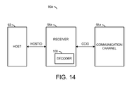
- FIG. 14 is a block diagram of an example implementation of another apparatus.
- Embodiments of the invention include providing device quality metrics using unsatisfied parity checks that may (i) count a number of failed checks during a portion of a decoding process, (ii) estimate how many read errors exist in uncorrected and/or uncorrectable read data, (iii) calculate the estimate without the decoding process converging, (iv) calculate the estimate without knowing the original error-free data, (v) determine a code rate of the data, (vi) be used for manufacturing qualification where the data is unknown and/or (vii) be implemented as one or more integrated circuits.
- Embodiments of the present invention provide a technique and/or apparatus that estimate a raw bit error rate (e.g., RBER) for data received from a device without having knowledge (possibly due to a lack of access) to the original error-free data conveyed by the device.
- the device is a storage device.
- the storage devices may include, but are not limited to, flash memory devices, solid-state drives, magnetic disk drives, optical drives, electro-magneto drives, tape drives and the like.
- the device is a communication device.
- the communication devices may include, but are not limited to, wired communication devices, wireless communication devices, optical communication device, radio frequency communication devices and the like.
- a code rate used to write a block of data (e.g., a codeword) is unknown.
- a code rate is defined as a number of user data symbols in a codeword divided by a total number of symbols in the codeword.
- the code rate that was used to encode the written data is determined, even in the presence of errors in the written data, by computing a normalized number of unsatisfied checks over the written data for all possible system code rates as quality metric (e.g., QM) values.
- QM quality metric
- a particular code rate that corresponds to a minimum value amongst the quality metric values is considered to be the estimated code rate of the written data.
- An advantage of the invention herein is that performing many potential iterations of the iterative decoding procedure to converge to a zero syndrome (e.g., correct all errors in a codeword) is avoided.
- the quality metric value is generally calculated within one or less iterations of the decoding process though more iterations may be run as appropriate. For instance, consider an adaptive coding scheme with N (e.g., 8) code rates with data encoded using a given code rate (e.g., code rate 0). Decoding is performed on one or more codewords at all N available code rates.
- the number of unsatisfied checks normalized by the codeword length for the given code rate is always the minimum value because the block is written using the given code rate.
- a single raw bit error causes q unsatisfied checks. Therefore, an almost linear relationship exists between the quality metrics and the raw bit error rate, especially at very low bit error rates when not many decoder iterations are run. The linear relationship can be used to calculate the raw bit error rate from the number of unsatisfied checks.
- a square-law, cubic-law, or higher order polynomial-law type fit for the relationship may be used for high accuracy, especially at high bit error rates to capture any non-linearity in the relationship.
- Other curve fitting routines may be implemented to meet the criteria of a particular application.
- the apparatus 90 implements a computer having a nonvolatile memory circuit.
- the apparatus 90 generally comprises a block (or circuit) 92 , a block (or circuit) 94 and a block (or circuit) 96 .
- the circuit 96 generally comprises a block (or circuit) 100 .
- the circuits 94 , 96 and 100 form a drive (or device) 102 .
- the circuits 92 to 102 may represent modules and/or blocks that may be implemented as hardware, software, a combination of hardware and software, or other implementations.
- One or more signals are exchanged between the circuit 92 and the circuit 96 .
- the host input/output signal HOSTIO generally includes, but is not limited to, a logical address component used to access data in the circuit 102 , a host command component that controls the circuit 102 , a write data component that transfers write data from the circuit 92 to the circuit 96 and a read data component that transfers error corrected read data from the circuit 96 to the circuit 92 .
- One or more signals are exchanged between the circuit 96 and the circuit 94 .
- the nonvolatile memory input/output signal NVMIO generally includes, but is not limited to, a physical address component used to access data in the circuit 94 , a memory command component that controls the circuit 94 (e.g., read or write commands), a write codeword component that carries error correction coded and cyclical redundancy check protected write codewords written from the circuit 96 into the circuit 94 and a read codeword component that carries the error correction coded codewords read from the circuit 94 to the circuit 96 .
- a physical address component used to access data in the circuit 94
- a memory command component that controls the circuit 94 (e.g., read or write commands)
- a write codeword component that carries error correction coded and cyclical redundancy check protected write codewords written from the circuit 96 into the circuit 94
- a read codeword component that carries the error correction coded codewords read from the circuit 94 to the circuit 96 .
- the circuit 92 is shown implemented as a host circuit.
- the circuit 92 is generally operational to read and write data to and from the circuit 94 via the circuit 96 .
- the circuit 92 transfers a logical address value in the signal HOSTIO to identify which set of data is to be written or to be read from the circuit 94 .
- the address generally spans a logical address range of the circuit 102 .
- the logical address can address individual data units, such as SATA (e.g., serial-ATA) sectors.
- the circuit 94 is shown implementing one or more nonvolatile memory circuits (or devices). According to various embodiments, the circuit 94 comprises one or more nonvolatile semiconductor devices. The circuit 94 is generally operational to store data in a nonvolatile condition. When data is read from the circuit 94 , the circuit 94 accesses a set of data (e.g., multiple bits) identified by the address (e.g., physical address) in the signal NVMIO. The address generally spans a physical address range of the circuit 94 .
- a set of data e.g., multiple bits
- the address e.g., physical address
- the circuit 96 is shown implementing a controller circuit.
- the circuit 96 is generally operational to control reading to and writing from the circuit 94 .
- the circuit 96 comprises one or more integrated circuits (or chips or die) implementing the controller of one or more solid-state drives (e.g., SSD), embedded storage, or other suitable control applications.
- SSD solid-state drives
- the circuit 100 is shown implemented as a decoder circuit.
- the circuit 100 is generally operational to decode the read codewords received from the circuit 94 .
- the resulting decoded data is presented to the circuit 92 via the signal HOSTIO and/or re-encoded and written back into the circuit 94 via the signal NVMIO.
- the circuit 100 generates a syndrome (each syndrome having multiple parity checks) by performing a syndrome computation process on the read codeword.
- the syndrome computation process is a portion less than all of an iterative decoding procedure.
- the syndrome computation process evaluates the read codeword using the H matrix of the code to determine which check equations are satisfied and which are not.
- the circuit 100 also generates a count value by counting a number of unsatisfied parity checks in the syndrome.
- the circuit 100 (or the circuit 96 ) generates a quality metric (e.g., QM) value of the circuit 94 (or the circuit 102 ) according to the count value.
- QM quality metric
- a transformation from the count value to the quality metic value may be achieved by a linear transformation, a cubic transformation, a formulaic computation, a polynomial transformation (e.g., a third-degree polynomial), a table look-up or other transformation.
- the transformation is according to the code rate. For example, the functions and/or coefficients thereof used in the transformation are selected according to the code rate.
- the functions and/or coefficients used in the transformation can be selected according to additional code parameters such as the column weight distribution, the row weight distribution, the decoding technique implemented in the circuit 100 or any other code attributes that can affect the relationship between the bit error rate and the number of unsatisfied checks.
- the circuit 102 is shown implementing a solid-state drive.
- the circuit 102 is generally operational to store data generated by the circuit 92 and return the data to the circuit 92 .
- the circuit 102 comprises one or more: nonvolatile semiconductor devices, such as NAND Flash devices, phase change memory (e.g., PCM) devices, or resistive RAM (e.g., ReRAM) devices; portions of a solid-state drive having one or more nonvolatile devices; and any other volatile or nonvolatile storage media.
- the circuit 102 is generally operational to store data in a nonvolatile condition.
- a granularity of about 1 bit per 4 unsatisfied checks may be determined, where a column-weight 4 code is assumed for the bit location.
- the relationship is a function of column weight.
- a column weight 3 low density parity check code e.g., LDPC
- the linearity range improves and the granularity improves.
- the final relationship of the number of unsatisfied checks and the raw bit error rate will be determined by the average of all code bit degrees.
- the unsatisfied checks can be determined in a number of ways, such as with just (M ⁇ 1)/M of an iteration of a layered decoder, where M is the number of layers in the parity direction of the layered decoder. Therefore, the metric is computed by less than a single iteration time at best. Furthermore, there is an almost linear relationship below bit error rates of 10 ⁇ 2 or up to the number of parity bits normalized by the codeword length.
- running more than a single iteration can result in a different number of unsatisfied checks per error bit, and hence the transformation from the quality metric to the raw bit error rate should be a function of the number of iterations run and the number of layers in a layered type decoder used in the computation.
- the method 120 is implemented in the circuit 100 , the circuit 96 and/or the circuit 102 .
- the method 120 generally comprises a step (or state). 122 , a step (or state) 124 , a step (or state) 126 , a step (or state) 128 , and a step (or state) 130 .
- the steps 122 to 130 may represent modules and/or blocks that may be implemented as hardware, software, a combination of hardware and software, or other implementations.
- Write data may be received by the circuit 96 from the circuit 92 .
- the circuit 96 encodes the write data at a given code rate using an encoding process (e.g., a low density parity check process at a code rate 0) in the step 122 .
- the encoded write data sometimes referred to as a codeword, is written into the circuit 94 by the circuit 96 in the step 124 .
- the circuit 96 reads the previously written codeword using a hard (e.g., binary) read technique.
- a hard e.g., binary
- the same outcome of step 126 can be reached if multiple hard reads, or a direct soft read occur as the desired hard read is a subset of the reads.
- the circuit 100 generates a quality metric (e.g., QM(K)) by running an initial portion of a decoding process (e.g., the low density parity check process) in the step 128 at a current code rate K.
- the quality metric QM(K) is generally the number of unsatisfied parity checks divided by the codeword length when using the parity check matrix of code K.
- the circuit 100 may initiate a repeat of the decoding process using a different code rate K if, for example, the code rate is not known a priori.
- the circuit 100 runs the initial portion of the decoding process on the read codeword at the different code rate.
- a loop between the steps 128 and 130 is repeated until all of the possible code rates have been checked.
- An estimation of the raw bit error rate is generated in the step 130 by identifying a lowest quality metric value and mapping that value to a bit error rate value.
- the step 130 ends the method 120 by generating one or more signals conveying (i) the estimated bit error rate value and (ii) a particular (estimated) code rate KK that resulted in the corresponding the lowest quality matric value.
- the method 130 is implemented in the circuit 100 , the circuit 96 and/or the circuit 102 .
- the method 130 generally comprises a step (or state) 132 , a step (or state) 134 , a step (or state) 136 , a step (or state) 138 , a step (or state) 140 , a step (or state) 142 , a step (or state) 144 , and a step (or state) 146 .
- the steps 132 to 146 may represent modules and/or blocks that may be implemented as hardware, software, a combination of hardware and software, or other implementations.
- the circuit 100 receives the read codeword from the circuit 94 .
- the value of P_MAX is the largest number of checks among the N codes.
- the quality metrics for the codeword as decoded using the code rate K are calculated.
- the just-calculated quality metric value QM(K) is better (e.g., having a lower value) than the current smallest quality metric value MIN_P.
- step 142 a check is made to see if any more code rates K remain to be checked. If code rates remain unchecked, the circuit 100 increments the current code rate K in the step 144 and returns to the step 136 . Once all of the code rates have been checked, the circuit 100 maps the surviving current smallest quality metric value MIN_P to a bit error rate in the step 146 using the stored transformation for the current code rate KK. The bit error rate and the current code rate are presented from the step 146 .
- FIG. 4 a graph of raw bit error rate versus normalized unsatisfied checks per low density parity check codeword for various code rates is shown, were the codewords are encoded using code rate 0.
- the normalized unsatisfied checks at the other code rates are all approximately the same (top horizontal line) and generally higher than the code rate 0 line.
- FIG. 5 a graph of raw bit error rate versus normalized unsatisfied checks per low density parity check codeword for various code rates is shown, where the codewords are encoded using code rate 7.
- the normalized unsatisfied checks at the other code rates are all approximately the same (top horizontal line) and higher than the code rate 7 line.
- FIG. 6 a graph of raw bit error rate versus unsatisfied checks per low density parity check codeword for the code rate 0 is shown. Simulations show that to a certain number of errors, the relationship with the number of unsatisfied checks is linear. The graph generally illustrates an approximately linear relationship between the unsatisfied checks and raw bit error per low density parity check codeword.
- FIG. 7 a graph of raw bit error rate versus unsatisfied checks per low density parity check codeword for the code rate 7 is shown.
- the graph generally illustrates an approximately linear relationship between the unsatisfied checks and raw bit error per low density parity check codeword.
- a graph of unsatisfied checks per low density parity check codeword for the code rate 0 versus raw bit error rate is shown.
- the graph shows a generally linear curve.
- a more accurate representation of the scatter plot curve may be achieved by applying a curve fitting routine to the data.
- the variable Y is the number of errors per codewords and the variable X is the number of unsatisfied checks per codeword.
- the higher ordered terms of the variable X may be dominated by the first order term.
- FIG. 9 a graph of a norm of residuals for the cubic curve fit for FIG. 8 is shown.
- the norm of residuals is approximately 503.
- Residuals below approximately 150 on the X-axis are correctable and have a bit error rate that varies by approximately ⁇ 3 percent.
- High bit error rates e.g., above approximately 250
- are uncorrectable and yield a larger spread of residuals e.g., ⁇ 20 percent).
- equations may be derived, such as by curve fitting, for the error bounds defined by the residuals as illustrated in FIG. 9 .
- equations may be derived to specify the degree of uncertainty, such as by confidence intervals.
- a graph of unsatisfied checks per low density parity check codeword for the code rate 7 versus raw bit error rate is shown.
- the graph shows a generally linear curve.
- FIG. 11 a graph of a norm of residuals for the cubic curve fit for FIG. 10 is shown.
- the norm of residuals is approximately 172.
- the code rate 7 covers a wider range of linearity and may be fitted to a cubic equation much more accurately than the code rate 0.
- a lower code rate furnishes a wider range of linearity.
- a graph of actual raw bit errors per low density parity check codeword for the code rate 1 versus estimated raw bit errors is shown.
- the graph and equation 4 show a generally linear relationship.
- a mean value and a median value of the estimation errors are approximately the same and generally range between 3 percent to 4 percent of the number of errors per low density parity check codeword.
- FIG. 14 a block diagram of an example implementation of an apparatus 90 a is shown.
- the apparatus (or circuit or device or integrated circuit) 90 a implements a computer connected to a communication system.
- the apparatus 90 a generally comprises the block 92 , a block (or circuit) 94 a and a block (or circuit) 96 a .
- the circuit 96 a generally comprises the block 100 .
- the circuits 92 a and 96 a may represent modules and/or blocks that may be implemented as hardware, software, a combination of hardware and software, or other implementations.
- the circuit 94 a is shown implementing a communication device.
- the circuit 94 a is operational to transfer codewords to the circuit 96 a via a signal (e.g., CCIO).
- the codewords are error correction coded when received by the circuit 96 a .
- the signal CCIO conveys the receive codewords from the circuit 94 a to the circuit 96 a .
- the signal CCIO conveys transmit codewords from the circuit 96 a to the circuit 94 a .
- the signal CCIO is bidirectional carrying codewords in both directions.
- the circuit 96 a is shown implementing a receiver circuit.
- the circuit 96 a is operational to receive error correction coded data from the circuit 94 a via a signal (e.g., CCIO).
- the circuit 96 a (through the circuit 100 ) corrects any errors in the received codewords and passes the corrected data to the circuit 92 in the signal HOSTIO.
- circuit 100 is shown as part of the circuits 96 and 96 a , the circuit 100 may be located differently in other embodiments.
- the circuit 100 may be located in the circuit 92 , a disk drive, at a point in a network (e.g., within the communication channel 94 a ), or other similar locations.
- bit error rate estimation can also be used with other encoding schemes, in addition to the low density parity check code.
- bit error rate estimation is suitable for any decode process that generates syndrome information.
- the decode processes include, but are not limited to polar codes and Bose Chaudhuri Hocquenghem (e.g., BCH) codes.
- Implementing decode processes that have a sparse H matrix provide an approximately linear relationship between the number of unsatisfied parity checks and the raw bit error rate.
- Using the syndrome information from a single or a few runs of an iterative decoding process also helps maintain the linear relationship between the raw bit error rate and the unsatisfied parity checks.
- multiple runs of the iterative decoding process are performed and a curve fit transformation (or mapping) is applied to the number of unsatisfied parity checks to calculate the raw bit error rate.
- the transformations between the number of unsatisfied parity checks and the raw bit error rate is typically determined off-line using random data with random errors.
- the decoder may provide the quality metric and/or the code rate used to write the data even if the decoding process does not converge, so the scheme works for scenarios in which the data is highly corrupted.
- An almost linear relationship exists below a bit error rate of approximately 10 ⁇ 2 or up to the (number of parity bits)/(codeword length).
- the quality metric scheme operates independently of which code rate was used to store the data in multi-coded system, as the linear time approach of the scheme blindly finds which code was used to encode the written data.
- FIGS. 1-3 and 14 may be implemented using one or more of a conventional general purpose processor, digital computer, microprocessor, microcontroller, RISC (reduced instruction set computer) processor, CISC (complex instruction set computer) processor, SIMD (single instruction multiple data) processor, signal processor, central processing unit (CPU), arithmetic logic unit (ALU), video digital signal processor (VDSP) and/or similar computational machines, programmed according to the teachings of the specification, as will be apparent to those skilled in the relevant art(s).
- RISC reduced instruction set computer
- CISC complex instruction set computer
- SIMD single instruction multiple data
- signal processor central processing unit
- CPU central processing unit
- ALU arithmetic logic unit
- VDSP video digital signal processor
- the invention may also be implemented by the preparation of ASICs (application specific integrated circuits), Platform ASICs, FPGAs (field programmable gate arrays), PLDs (programmable logic devices), CPLDs (complex programmable logic devices), sea-of-gates, RFICs (radio frequency integrated circuits), ASSPs (application specific standard products), one or more monolithic integrated circuits, one or more chips or die arranged as flip-chip modules and/or multi-chip modules or by interconnecting an appropriate network of conventional component circuits, as is described herein, modifications of which will be readily apparent to those skilled in the art(s).
- ASICs application specific integrated circuits
- FPGAs field programmable gate arrays
- PLDs programmable logic devices
- CPLDs complex programmable logic devices
- sea-of-gates RFICs (radio frequency integrated circuits)
- ASSPs application specific standard products
- monolithic integrated circuits one or more chips or die arranged as flip-chip modules and/or multi-chip modules
- the invention thus may also include a computer product which may be a storage medium or media and/or a transmission medium or media including instructions which may be used to program a machine to perform one or more processes or methods in accordance with the invention.
- a computer product which may be a storage medium or media and/or a transmission medium or media including instructions which may be used to program a machine to perform one or more processes or methods in accordance with the invention.
- Execution of instructions contained in the computer product by the machine, along with operations of surrounding circuitry, may transform input data into one or more files on the storage medium and/or one or more output signals representative of a physical object or substance, such as an audio and/or visual depiction.
- the storage medium may include, but is not limited to, any type of disk including floppy disk, hard drive, magnetic disk, optical disk, CD-ROM, DVD and magneto-optical disks and circuits such as ROMs (read-only memories), RAMS (random access memories), EPROMs (erasable programmable ROMs), EEPROMs (electrically erasable programmable ROMs), UVPROM (ultra-violet erasable programmable ROMs), Flash memory, magnetic cards, optical cards, and/or any type of media suitable for storing electronic instructions.
- ROMs read-only memories
- RAMS random access memories
- EPROMs erasable programmable ROMs
- EEPROMs electrically erasable programmable ROMs
- UVPROM ultra-violet erasable programmable ROMs
- Flash memory magnetic cards, optical cards, and/or any type of media suitable for storing electronic instructions.
- the elements of the invention may form part or all of one or more devices, units, components, systems, machines and/or apparatuses.
- the devices may include, but are not limited to, servers, workstations, storage array controllers, storage systems, personal computers, laptop computers, notebook computers, palm computers, personal digital assistants, portable electronic devices, battery powered devices, set-top boxes, encoders, decoders, transcoders, compressors, decompressors, pre-processors, post-processors, transmitters, receivers, transceivers, cipher circuits, cellular telephones, digital cameras, positioning and/or navigation systems, medical equipment, heads-up displays, wireless devices, audio recording, audio storage and/or audio playback devices, video recording, video storage and/or video playback devices, game platforms, peripherals and/or multi-chip modules.
- Those skilled in the relevant art(s) would understand that the elements of the invention may be implemented in other types of devices to meet the criteria of a particular application.
Abstract
Description
Y=1.774×10−6 X 3−5.95×10−5 X 2+0.271X−0.197 (1)
The variable Y is the number of errors per codewords and the variable X is the number of unsatisfied checks per codeword. The higher ordered terms of the variable X may be dominated by the first order term. As such,
Y=0.271X−0.197 (2)
Equation 2 shows the general linear relationship.
Y=2.33×10−8 X 3+6.04×10−5 X 2+0.24971X+0.00255 (3)
Y=7.84×10−7 X 3+7.51×10−5 X 2+0.26X+0.084 (4)
The graph and equation 4 show a generally linear relationship.
Claims (20)
Priority Applications (2)
| Application Number | Priority Date | Filing Date | Title |
|---|---|---|---|
| US14/101,679 US9489256B2 (en) | 2013-11-07 | 2013-12-10 | Device quality metrics using unsatisfied parity checks |
| US15/297,574 US9817708B2 (en) | 2013-11-07 | 2016-10-19 | Device quality metrics using unsatisfied parity checks |
Applications Claiming Priority (2)
| Application Number | Priority Date | Filing Date | Title |
|---|---|---|---|
| US201361901064P | 2013-11-07 | 2013-11-07 | |
| US14/101,679 US9489256B2 (en) | 2013-11-07 | 2013-12-10 | Device quality metrics using unsatisfied parity checks |
Related Child Applications (1)
| Application Number | Title | Priority Date | Filing Date |
|---|---|---|---|
| US15/297,574 Continuation US9817708B2 (en) | 2013-11-07 | 2016-10-19 | Device quality metrics using unsatisfied parity checks |
Publications (2)
| Publication Number | Publication Date |
|---|---|
| US20150128006A1 US20150128006A1 (en) | 2015-05-07 |
| US9489256B2 true US9489256B2 (en) | 2016-11-08 |
Family
ID=53007993
Family Applications (2)
| Application Number | Title | Priority Date | Filing Date |
|---|---|---|---|
| US14/101,679 Active 2034-05-14 US9489256B2 (en) | 2013-11-07 | 2013-12-10 | Device quality metrics using unsatisfied parity checks |
| US15/297,574 Active US9817708B2 (en) | 2013-11-07 | 2016-10-19 | Device quality metrics using unsatisfied parity checks |
Family Applications After (1)
| Application Number | Title | Priority Date | Filing Date |
|---|---|---|---|
| US15/297,574 Active US9817708B2 (en) | 2013-11-07 | 2016-10-19 | Device quality metrics using unsatisfied parity checks |
Country Status (1)
| Country | Link |
|---|---|
| US (2) | US9489256B2 (en) |
Cited By (1)
| Publication number | Priority date | Publication date | Assignee | Title |
|---|---|---|---|---|
| US20170039098A1 (en) * | 2013-11-07 | 2017-02-09 | Seagate Technology Llc | Device quality metrics using unsatisfied parity checks |
Families Citing this family (11)
| Publication number | Priority date | Publication date | Assignee | Title |
|---|---|---|---|---|
| US9459956B2 (en) | 2013-07-19 | 2016-10-04 | Seagate Technology Llc | Data decoder with trapping set flip bit mapper |
| US9317361B2 (en) * | 2013-11-27 | 2016-04-19 | Seagate Technology Llc | Bit-line defect detection using unsatisfied parity code checks |
| US10078540B2 (en) * | 2014-06-13 | 2018-09-18 | Cisco Technology, Inc. | Accurate and fast in-service estimation of input bit error ratio of low density parity check decoders |
| WO2017217711A1 (en) * | 2016-06-14 | 2017-12-21 | 엘지전자 주식회사 | Data retransmission method for polar code, and device therefor |
| US10644829B2 (en) | 2016-09-15 | 2020-05-05 | Huawei Technologies Co., Ltd. | Method and apparatus for encoding data using a polar code |
| US10218384B2 (en) | 2016-12-01 | 2019-02-26 | Sandisk Technologies Llc | ECC decoder with multiple decoding modes |
| US10565040B2 (en) | 2016-12-01 | 2020-02-18 | Western Digital Technologies, Inc. | ECC decoder with selective component disabling based on decoding message resolution |
| US10530393B2 (en) * | 2016-12-01 | 2020-01-07 | Western Digital Technologies, Inc. | Configurable ECC decoder |
| WO2018176478A1 (en) * | 2017-04-01 | 2018-10-04 | Qualcomm Incorporated | Communication system and method having polar coding with two concatenated cyclic redundancy check codes |
| CA3161454A1 (en) | 2019-11-13 | 2021-05-20 | Fluid-Screen, Inc. | Methods and apparatus for detection of bacteria in a sample using dielectrophoresis |
| US20240103727A1 (en) * | 2022-09-22 | 2024-03-28 | SK Hynix Inc. | Out-of-order bit-flipping decoders for non-volatile memory devices |
Citations (11)
| Publication number | Priority date | Publication date | Assignee | Title |
|---|---|---|---|---|
| US20080126908A1 (en) * | 2006-07-25 | 2008-05-29 | Communications Coding Corporation | Universal error control coding system for digital communication and data storage systems |
| US7454685B2 (en) | 2004-11-23 | 2008-11-18 | Samsung Electronics Co., Ltd. | Method and apparatus for decoding low density parity check code using united node processing |
| US20110202816A1 (en) | 2007-07-02 | 2011-08-18 | Broadcom Corporation | Distributed processing LDPC (Low Density Parity Check) decoder |
| US20110246862A1 (en) * | 2010-03-31 | 2011-10-06 | Nils Graef | Hard input low density parity check decoder |
| US20110320902A1 (en) * | 2010-06-29 | 2011-12-29 | Lsi Corporation | Conditional skip-layer decoding |
| US8381074B1 (en) | 2010-05-21 | 2013-02-19 | Lsi Corporation | Systems and methods for utilizing a centralized queue based data processing circuit |
| US8413010B1 (en) | 2009-03-12 | 2013-04-02 | Western Digital Technologies, Inc. | Data storage device employing high quality metrics when decoding logical block address appended to a data sector |
| US20130145085A1 (en) * | 2008-06-18 | 2013-06-06 | Super Talent Technology Corp. | Virtual Memory Device (VMD) Application/Driver with Dual-Level Interception for Data-Type Splitting, Meta-Page Grouping, and Diversion of Temp Files to Ramdisks for Enhanced Flash Endurance |
| US8499227B2 (en) | 2010-09-23 | 2013-07-30 | Micron Technology, Inc. | Memory quality monitor based compensation method and apparatus |
| US20150149855A1 (en) * | 2013-11-27 | 2015-05-28 | Lsi Corporation | Bit-line defect detection using unsatisified parity code checks |
| US9059742B1 (en) * | 2013-03-15 | 2015-06-16 | Western Digital Technologies, Inc. | System and method for dynamic scaling of LDPC decoder in a solid state drive |
Family Cites Families (1)
| Publication number | Priority date | Publication date | Assignee | Title |
|---|---|---|---|---|
| US9489256B2 (en) * | 2013-11-07 | 2016-11-08 | Seagate Technology Llc | Device quality metrics using unsatisfied parity checks |
-
2013
- 2013-12-10 US US14/101,679 patent/US9489256B2/en active Active
-
2016
- 2016-10-19 US US15/297,574 patent/US9817708B2/en active Active
Patent Citations (11)
| Publication number | Priority date | Publication date | Assignee | Title |
|---|---|---|---|---|
| US7454685B2 (en) | 2004-11-23 | 2008-11-18 | Samsung Electronics Co., Ltd. | Method and apparatus for decoding low density parity check code using united node processing |
| US20080126908A1 (en) * | 2006-07-25 | 2008-05-29 | Communications Coding Corporation | Universal error control coding system for digital communication and data storage systems |
| US20110202816A1 (en) | 2007-07-02 | 2011-08-18 | Broadcom Corporation | Distributed processing LDPC (Low Density Parity Check) decoder |
| US20130145085A1 (en) * | 2008-06-18 | 2013-06-06 | Super Talent Technology Corp. | Virtual Memory Device (VMD) Application/Driver with Dual-Level Interception for Data-Type Splitting, Meta-Page Grouping, and Diversion of Temp Files to Ramdisks for Enhanced Flash Endurance |
| US8413010B1 (en) | 2009-03-12 | 2013-04-02 | Western Digital Technologies, Inc. | Data storage device employing high quality metrics when decoding logical block address appended to a data sector |
| US20110246862A1 (en) * | 2010-03-31 | 2011-10-06 | Nils Graef | Hard input low density parity check decoder |
| US8381074B1 (en) | 2010-05-21 | 2013-02-19 | Lsi Corporation | Systems and methods for utilizing a centralized queue based data processing circuit |
| US20110320902A1 (en) * | 2010-06-29 | 2011-12-29 | Lsi Corporation | Conditional skip-layer decoding |
| US8499227B2 (en) | 2010-09-23 | 2013-07-30 | Micron Technology, Inc. | Memory quality monitor based compensation method and apparatus |
| US9059742B1 (en) * | 2013-03-15 | 2015-06-16 | Western Digital Technologies, Inc. | System and method for dynamic scaling of LDPC decoder in a solid state drive |
| US20150149855A1 (en) * | 2013-11-27 | 2015-05-28 | Lsi Corporation | Bit-line defect detection using unsatisified parity code checks |
Cited By (2)
| Publication number | Priority date | Publication date | Assignee | Title |
|---|---|---|---|---|
| US20170039098A1 (en) * | 2013-11-07 | 2017-02-09 | Seagate Technology Llc | Device quality metrics using unsatisfied parity checks |
| US9817708B2 (en) * | 2013-11-07 | 2017-11-14 | Seagate Technology Llc | Device quality metrics using unsatisfied parity checks |
Also Published As
| Publication number | Publication date |
|---|---|
| US20150128006A1 (en) | 2015-05-07 |
| US9817708B2 (en) | 2017-11-14 |
| US20170039098A1 (en) | 2017-02-09 |
Similar Documents
| Publication | Publication Date | Title |
|---|---|---|
| US9817708B2 (en) | Device quality metrics using unsatisfied parity checks | |
| US9317361B2 (en) | Bit-line defect detection using unsatisfied parity code checks | |
| US10135465B2 (en) | Error correction methods and apparatuses using first and second decoders | |
| US9673840B2 (en) | Turbo product codes for NAND flash | |
| US9021332B2 (en) | Flash memory read error recovery with soft-decision decode | |
| US9329935B2 (en) | Method to dynamically update LLRs in an SSD drive and/or controller | |
| US9319073B2 (en) | Mitigation of write errors in multi-level cell flash memory through adaptive error correction code decoding | |
| US9990247B2 (en) | Write mapping to mitigate hard errors via soft-decision decoding | |
| US10135464B2 (en) | Reliability-assisted bit-flipping decoding algorithm | |
| US9405624B2 (en) | On-die error detection and correction during multi-step programming | |
| US20150333776A1 (en) | Decoding based on randomized hard decisions | |
| US10153052B2 (en) | Flash command that reports a count of cell program failures | |
| US9304851B2 (en) | Decoding with log likelihood ratios stored in a controller | |
| US10514980B2 (en) | Encoding method and memory storage apparatus using the same | |
| US10771094B2 (en) | Memory system configured to estimate a read voltage using a histogram | |
| US20170134053A1 (en) | Fixed point conversion of llr values based on correlation | |
| KR20180123393A (en) | Siso decoding method, decoder and semiconductor memory system using the same | |
| US9405480B2 (en) | Interleaving codewords over multiple flash planes | |
| KR102226174B1 (en) | Iterative decoder, decoding method and semiconductor memory system | |
| US10740176B2 (en) | Computing system with shift adjustable coding mechanism and method of operation thereof | |
| KR20170067656A (en) | Turbo product codes for nand flash |
Legal Events
| Date | Code | Title | Description |
|---|---|---|---|
| AS | Assignment |
Owner name: LSI CORPORATION, CALIFORNIA Free format text: ASSIGNMENT OF ASSIGNORS INTEREST;ASSIGNORS:ALHUSSIEN, ABDELHAKIM S;COHEN, EARL T.;HARATSCH, ERICH F.;SIGNING DATES FROM 20131126 TO 20131210;REEL/FRAME:031791/0582 |
|
| AS | Assignment |
Owner name: DEUTSCHE BANK AG NEW YORK BRANCH, AS COLLATERAL AG Free format text: PATENT SECURITY AGREEMENT;ASSIGNORS:LSI CORPORATION;AGERE SYSTEMS LLC;REEL/FRAME:032856/0031 Effective date: 20140506 |
|
| AS | Assignment |
Owner name: SEAGATE TECHNOLOGY LLC, CALIFORNIA Free format text: ASSIGNMENT OF ASSIGNORS INTEREST;ASSIGNOR:LSI CORPORATION;REEL/FRAME:034773/0839 Effective date: 20140902 |
|
| AS | Assignment |
Owner name: LSI CORPORATION, CALIFORNIA Free format text: TERMINATION AND RELEASE OF SECURITY INTEREST IN PATENT RIGHTS (RELEASES RF 032856-0031);ASSIGNOR:DEUTSCHE BANK AG NEW YORK BRANCH, AS COLLATERAL AGENT;REEL/FRAME:037684/0039 Effective date: 20160201 Owner name: AGERE SYSTEMS LLC, PENNSYLVANIA Free format text: TERMINATION AND RELEASE OF SECURITY INTEREST IN PATENT RIGHTS (RELEASES RF 032856-0031);ASSIGNOR:DEUTSCHE BANK AG NEW YORK BRANCH, AS COLLATERAL AGENT;REEL/FRAME:037684/0039 Effective date: 20160201 |
|
| STCF | Information on status: patent grant |
Free format text: PATENTED CASE |
|
| MAFP | Maintenance fee payment |
Free format text: PAYMENT OF MAINTENANCE FEE, 4TH YEAR, LARGE ENTITY (ORIGINAL EVENT CODE: M1551); ENTITY STATUS OF PATENT OWNER: LARGE ENTITY Year of fee payment: 4 |