US9479756B2 - Stereo camera device - Google Patents
Stereo camera device Download PDFInfo
- Publication number
- US9479756B2 US9479756B2 US14/783,354 US201414783354A US9479756B2 US 9479756 B2 US9479756 B2 US 9479756B2 US 201414783354 A US201414783354 A US 201414783354A US 9479756 B2 US9479756 B2 US 9479756B2
- Authority
- US
- United States
- Prior art keywords
- casing
- stereo camera
- substrate
- camera device
- radiation noise
- Prior art date
- Legal status (The legal status is an assumption and is not a legal conclusion. Google has not performed a legal analysis and makes no representation as to the accuracy of the status listed.)
- Active
Links
Images


Classifications
-
- H04N13/0203—
-
- H—ELECTRICITY
- H04—ELECTRIC COMMUNICATION TECHNIQUE
- H04N—PICTORIAL COMMUNICATION, e.g. TELEVISION
- H04N13/00—Stereoscopic video systems; Multi-view video systems; Details thereof
- H04N13/20—Image signal generators
- H04N13/204—Image signal generators using stereoscopic image cameras
-
- H04N13/0239—
-
- H—ELECTRICITY
- H04—ELECTRIC COMMUNICATION TECHNIQUE
- H04N—PICTORIAL COMMUNICATION, e.g. TELEVISION
- H04N13/00—Stereoscopic video systems; Multi-view video systems; Details thereof
- H04N13/20—Image signal generators
- H04N13/204—Image signal generators using stereoscopic image cameras
- H04N13/239—Image signal generators using stereoscopic image cameras using two two-dimensional [2D] image sensors having a relative position equal to or related to the interocular distance
-
- H—ELECTRICITY
- H04—ELECTRIC COMMUNICATION TECHNIQUE
- H04N—PICTORIAL COMMUNICATION, e.g. TELEVISION
- H04N23/00—Cameras or camera modules comprising electronic image sensors; Control thereof
- H04N23/50—Constructional details
- H04N23/51—Housings
-
- H—ELECTRICITY
- H04—ELECTRIC COMMUNICATION TECHNIQUE
- H04N—PICTORIAL COMMUNICATION, e.g. TELEVISION
- H04N25/00—Circuitry of solid-state image sensors [SSIS]; Control thereof
- H04N25/60—Noise processing, e.g. detecting, correcting, reducing or removing noise
- H04N25/617—Noise processing, e.g. detecting, correcting, reducing or removing noise for reducing electromagnetic interference, e.g. clocking noise
-
- H04N5/2252—
-
- H04N5/357—
-
- H—ELECTRICITY
- H05—ELECTRIC TECHNIQUES NOT OTHERWISE PROVIDED FOR
- H05K—PRINTED CIRCUITS; CASINGS OR CONSTRUCTIONAL DETAILS OF ELECTRIC APPARATUS; MANUFACTURE OF ASSEMBLAGES OF ELECTRICAL COMPONENTS
- H05K9/00—Screening of apparatus or components against electric or magnetic fields
- H05K9/0007—Casings
- H05K9/002—Casings with localised screening
- H05K9/0022—Casings with localised screening of components mounted on printed circuit boards [PCB]
- H05K9/0037—Housings with compartments containing a PCB, e.g. partitioning walls
-
- G—PHYSICS
- G03—PHOTOGRAPHY; CINEMATOGRAPHY; ANALOGOUS TECHNIQUES USING WAVES OTHER THAN OPTICAL WAVES; ELECTROGRAPHY; HOLOGRAPHY
- G03B—APPARATUS OR ARRANGEMENTS FOR TAKING PHOTOGRAPHS OR FOR PROJECTING OR VIEWING THEM; APPARATUS OR ARRANGEMENTS EMPLOYING ANALOGOUS TECHNIQUES USING WAVES OTHER THAN OPTICAL WAVES; ACCESSORIES THEREFOR
- G03B17/00—Details of cameras or camera bodies; Accessories therefor
- G03B17/02—Bodies
-
- H—ELECTRICITY
- H04—ELECTRIC COMMUNICATION TECHNIQUE
- H04N—PICTORIAL COMMUNICATION, e.g. TELEVISION
- H04N2213/00—Details of stereoscopic systems
- H04N2213/001—Constructional or mechanical details
Definitions
- the present invention relates to a stereo camera device.
- a camera module having such a structure that a partition plate is provided between an imaging element and an image-processing substrate, and noise generated in the substrate is not transmitted to the imaging element (e.g., PTL 1).
- a stereo camera device described in claim 1 including: a casing, a first imaging portion provided on one of ends of the casing in a longitudinal direction of the stereo camera device, a second imaging portion provided on the other end of the casing in the longitudinal direction, a substrate on which a processing circuit connected to the first imaging portion and the second imaging portion through signal lines is mounted, on which a connector for outputting a signal processed by the processing unit to an external device is placed, and which is provided, in the casing, and at least one partition for dividing an interior of the casing into a plurality of spaces in the longitudinal direction at first intervals corresponding to a frequency band which suppresses radiation noise from the signal lines.
- the present invention since a partition is provided, to divide the interior of the casing at the first intervals which correspond to frequency of the radiation noise from the signal line, it is possible to prevent an adverse influence from being exerted on an external device caused by the radiation noise.
- FIG. 1 is a perspective view for describing an interior structure of a stereo camera device according to a first embodiment of the present invention.
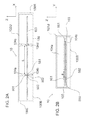
- FIGS. 2A and 2B are sectional views of the stereo camera device of the first embodiment.
- FIG. 3 is a schematic plan view of an upper surface of a substrate provided in a casing.
- FIG. 4 is a diagram for describing cavity resonance in a space divided in the casing.
- FIGS. 5A and 5B are sectional views of a stereo camera device according to a second embodiment.
- FIG. 6 is a perspective: view for describing an interior structure of a stereo camera device according to a third embodiment.
- FIG. 7 is a sectional view of a stereo camera device according to a modification.
- FIG. 1 is a transmissive schematic perspective view of an interior structure of the stereo camera device according to the first embodiment.
- the present invention will be described below based on the assumption that a coordinate system composed of an x axis, a y axis and a z axis is set as shown in the drawings.
- the stereo camera device 10 includes a metal casing 100 , a first imaging portion 101 , a second imaging portion 102 , a substrate 103 , partition plates 104 a , 104 b , 104 c and 104 d (when they are collectively called, reference sign 104 is assigned), an image processing IC 108 , a microcomputer 109 , a connector 110 and signal lines 111 and 112 .
- the casing 100 has such a cylindrical shape that its long side (longitudinal direction) extends in an x-axis direction. While a cross section shape of the casing 100 at a plane intersecting with the x axis at right angles is rectangular in the example shown in FIG. 1 , the cross section shape is determined in associated with an installation place of the stereo camera device 10 , and a circular cross section shape or an elliptic cross section shape are also included in one embodiment of the present invention.
- the first imaging portion 101 is formed by mounting an imaging element and an optical lens (both not shown), and the first imaging portion 101 is placed on one of ends ( ⁇ side of x-axis in FIG. 1 ) of the casing 100 .
- the second imaging portion 102 is formed by mounting an imaging element and an optical lens (both not shown), and the first imaging portion 101 is placed on the other end (+side of x-axis in FIG. 1 ) of the casing 100 . That is, the first imaging portion 101 and the second imaging portion 102 are placed in the casing 100 such that the imaging portions 101 and 102 are separated from each other by a reference length L 0 along the x axis which is the longitudinal direction.
- the first imaging portion 101 and the second imaging portion 102 shoot (take a picture of) a photogenic subject on the y-axis +side, and output, to a later-described image processing IC 1 . 08 , an analogue image signal produced by photoelectric conversion.
- the first imaging portion 101 and the second imaging portion 102 configuring the stereo camera device 10 are controlled such that image control and sending and receiving operations of signals are carried out substantially at the same time.
- the substrate 103 extends in the x-axis direction, i.e., the longitudinal direction of the casing 100 , and the substrate 103 is placed in the casing 100 by sandwiching the substrate 103 from the +side of z-axis by the partition plates 104 a and 104 c and from the ⁇ side of z-axis by the partition plates 104 b and 104 d .
- a ⁇ side end of x-axis and a +side end of x-axis of the substrate 103 are connected to each other through the first imaging portion 101 and the second imaging portion 102 , a cable or a connector.
- the image processing IC 108 , the microcomputer 109 , the connector 110 , the signal lines 111 and 112 and various IC (not shown) are provided on the substrate 103 .
- a circuit GND pattern (wire) or a frame GND pattern (wire) are provided in the y-axis direction at a position where the pattern is connected to the later-described partition plate 104 .
- the image processing IC 108 is connected to the first imaging portion 101 through the signal line 111 and connected to the second imaging portion 102 through the signal line 112 .
- the image processing IC 108 sends and receives various control signals and analog image signals between the first imaging portion 101 and the second imaging portion 102 , converts the received image signal into a digital signal, and calculates a distance to the shot object and a size of the object.
- the microcomputer 109 is a control circuit which controls the image processing IC 108 .
- the connector 110 supplies power source to various ICs provided on the substrate 103 , and outputs a shot image and the like processed by the image processing IC 108 to an in-vehicle external device such as a car radio and a navigation system.
- the signal lines 111 and 112 are places using ends on the substrate 103 as paths such that the signal lines 111 and 112 can avoid the various ICs and wires provided on the substrate 103 . While FIG. 1 shows the example that the image processing IC 108 and the microcomputer 109 are placed in the vicinity of a central portion of the substrate 103 , the places where the image processing IC 108 and the microcomputer 109 are placed are not limited to the example shown in FIG. 1 .
- the partition plates 104 are metal plate members provided to prevent, radiation noise from the signal lines 111 and 112 from being transmitted to the external device through the connector 110 and from exerting adverse influence.
- the partition plates 104 a and 104 c are mounted on an upper surface 100 U of the casing 100 through a screw or weld.
- the partition plates 104 b and 104 d are mounted on a bottom surface 100 B of the casing 100 through a screw or weld.
- Across section of each of the partition plates 104 at a plane which is parallel to a yz-plane is formed into a rectangular shape such that an interior of the casing 100 is divided into a plurality of spaces in the x-axis direction.
- a length L of each of the plurality of spaces divided by the partition plates 104 in the x-axis direction i.e., an interval between the partition prates 104 a and 104 c , an interval between the partition plates 104 b and 104 d , an interval between the side surface 100 L of the casing 100 and the partition plates 104 a and 104 b , and an interval between a side surface 100 R of the casing 100 and the partition plates 104 c and 104 d are determined in accordance with a frequency band which suppresses radiation noise from the signal lines 111 and 112 . Details of the length L will be described later. Thicknesses of the partition plates 104 are determined such that strength against vibration is secured.
- the partition plates 104 may integrally be formed together with the casing 100 .
- FIG. 2( a ) is a sectional view of the casing 100 in an xz-plane
- FIG. 2( b ) is a sectional view of the casing 100 in a yz-plane. While the following description is made centering on the partition plates 104 a and 104 b , the partition plates 104 c and 104 d also have, the same configurations.
- the partition plate 104 a is connected to a circuit GND pattern or a frame GND pattern (collectively called ground pattern, hereinafter) 550 provided on an upper surface of the substrate 103 through the ground member 501 made of resilient material, such as a spring.
- a partition plate 104 b is connected to a ground pattern 551 provided on a lower surface of the substrate 103 through the ground member 502 made of radiation noise such as a spring.
- the partition plates 104 a and 104 b and the ground members 501 and 502 are integrally formed respectively.
- the plurality of ground members 501 and 502 are provided at predetermined intervals a in a y-axis direction, i.e., a short direction of the casing 100 . That is, the partition plates 104 a and 104 b are connected to the substrate 103 in a separated manner at the predetermined intervals a in the y-axis direction.
- the space between the substrate 103 and the partition plate 104 function as a waveguide, and the waveguide prevents radiation noise of predetermined frequency or less generated from the signal lines 111 and 112 from being transmitted to the external device through the connector 110 and from exerting adverse influence.
- the ground member 501 of the partition plate 104 a and the ground member 502 of the partition plate 104 b are provided substantially on the same straight line in the z-axis direction. Hence, it is possible to enhance a hidden degree of the spaces divided by the partition plates 104 a and 104 b in the x-axis direction. Further, the substrate 103 sandwiched between the partition plates 104 a and 104 b is sandwiched from the +side and ⁇ side of z-axis substantially by the same forces through the ground members 501 and 502 made of resilient material, and it is possible to prevent the substrate 103 from bending.
- FIG. 3 is a schematic plan view of the upper surface of the substrate 103 when the interior of the casing 100 is viewed from the +direction of z-axis.
- the signal lines 111 and 112 are provided as paths using ends on the substrate 103 such that the signal lines 111 and 112 avoid she various ICs and the wires provided on the substrate 103 .
- the ends of the substrate 103 do not easily take return pass of the GND pattern, noise is prone to be radiated from the signal lines 111 and 112 .
- the signal lines 111 and 112 connect, to each other, the image processing IC 108 provided in the vicinity of a central portion of the upper surface of the substrate 103 and the first imaging portion 101 on the +side of the x-axis and the second imaging portion 102 on the ⁇ side of x-axis.
- wiring paths of the signal lines 111 and 112 have shapes of dipole antenna as described above.
- signals are transmitted to the signal lines 111 and 112 substantially at the same time.
- the signal lines 111 and 112 function as dipole antenna, and noise is prone to be generated.
- Noises generated by the signal lines 111 and 112 occur resonance phenomenon in the space of the cylindrical, casing 100 having the long side in the x-axis direction, and become noises (radiation noises) having high frequency (resonance frequency).
- this radiation noise is transmitted to the connector 110 and is discharged to the outside of the stereo camera device 10 or the radiation noise leaks to outside from a gap of the casing 100 , the radiation noise exerts adverse influence on the operation of the in-vehicle external device depending upon frequency of the radiation noise.
- the frequency of the radiation noise is brought into cavity resonance frequency f 1 of a frequency band which is higher than a frequency band having the possibility of adverse influence exerted on the operation of the external device, and influence on the operation of the external device, is lowered.
- the length L of the space divided in the casing 100 in the x-axis direction is determined such that frequency becomes the cavity resonance frequency f 1 which does no exert adverse influence on the operation of the external device.
- the cavity resonance frequency f 1 is indicated by the following equation (1).
- f 1 1.50 ⁇ (1/ L ) 2 +( m/M ) 2 +( n/N ) 2 ⁇ 1/2 [MHz] (1)
- L, M and N are lengths of the divided spaces in the x axis, the y axis and the z axis. Further, l, m and n shows the number of half wavelengths in the spaces divided in the casing 100 .
- the cavity resonance frequency f 1 can be expressed by the following equation (2) which is similar to the equation (1). As shown in equation (2), the smaller the length L of the divided space becomes, the higher the cavity resonance frequency f 1 becomes. f 1 ⁇ 150 ⁇ (1/ L ) [MHz] (2)
- a waveform W 1 shown by a solid line in FIG. 4 shows one half wavelength forming one node in the space.
- Waveforms W 2 shown by a broken line show three half wavelengths forming three nodes in the space.
- the cavity resonance frequency f 1 of radiation noise is set to not less than certain frequency (e.g., about 3 [GHz]) which is higher than the highest frequency of a noise spec of each of the external devices.
- certain frequency e.g., about 3 [GHz]
- the length L of the divided space in the x-axis direction is set to 5 [cm] or less.
- the partition plates 104 a , 104 b , 104 c and 104 d are provided in the casing 100 such that the interval between the partition plates 104 a and 104 c in the x-axis, the interval between the partition plates 104 b and 104 d in the x-axis, the interval between the side surface 100 L of the casing 100 and the partition plates 104 a and 104 b in the x-axis direction, and the interval between a side surface 100 R of the casing 100 and the partition plates 104 c and 104 d in the x-axis direction shown in FIG. 2 become 5 [cm] or less.
- the lower limit of the interval in the x-axis be determined while taking into consideration, costs of the partition plates 104 , installation of the various ICs and parts on the substrate 103 and difficulties of pattern design.
- the cavity resonance frequency f 1 becomes a frequency band higher than a frequency band which exerts adverse influence on the external device. Hence, even if radiation noise which becomes the cavity resonance frequency f 1 is discharged outside of the stereo camera device 10 through the connector 110 or the radiation noise leaks to outside from the gap of the casing 100 , adverse influence is not exerted on the operation of the external device.
- the above description is based on the example that the interior of the casing 100 is divided into the three spaces by the partition plates 104 .
- the number of divided spaces i.e., the number of the partition plates 104 provided in the casing 100 differs depending upon radiation noises from the signal lines 111 and 112 and the length of the casing 100 in the x-axis direction.
- the partition plates 104 are connected to the substrate 103 at the predetermined interval a in the y-axis such that the partition plates are separated from the substrate 103 as described above. According to this, the spaces existing between the partition plates 104 and the substrate 103 in the z-axis direction function as waveguides.
- the cutoff frequency f 2 is a frequency band having nothing to do with the operation of the stereo camera device 10 .
- the cutoff frequency f 2 is set to a frequency component which does not reach the cavity resonance frequency f 1 by the partition plates 101 and especially, the cutoff frequency f 2 is set to a frequency band having the possibility of adverse influence exerted on the external device. That is, it is preferable that the cutoff frequency f 2 be set to a value smaller than the cavity resonance frequency f 1 .
- the predetermined interval a is determined based on the equation (3) so that such cutoff frequency f 2 is obtained. That is, the predetermined interval a is determined such that radiation noise from the signal lines 111 and 112 which is equal to or less than the cutoff frequency f 2 is cut off, and the radiation noise which is equal to or less than the cutoff frequency f 2 is prevented from passing from the spaces.
- radiation noise from the signal lines 111 and 112 includes a frequency band exerting adverse influence on the external device is cut off. This configuration prevents radiation noise from the signal lines 111 and 112 from being transmitted to the external device through the connector 110 and from exerting di.
- FIG. 2( b ) shows a case where five ground members 501 and 502 are provided respectively.
- the number of ground members 501 and 502 is determined in associated with the predetermined interval a, and it is preferable that at least one pair of ground members 501 and 502 be provided respectively.
- the stereo camera device includes the partition plates 104 dividing the interior of the cylindrical casing 100 into the plurality of spaces in the longitudinal direction at an interval corresponding to a frequency band suppressing radiation noise from the signal lines 111 and 112 which connect, to each other, the first imaging portion 101 , the second imaging portion 102 provided on both ends in the longitudinal direction and the image processing IC 108 .
- This interval is determined such that the cavity resonance frequency f 1 of a frequency band becomes higher than a frequency band of noise radiated from the signal lines 111 and 112 .
- the partition plates 104 a and 104 c provided on an inner wall of the upper surface 100 U of the casing 100 are connected to each other through the ground pattern 550 and the ground member 501 provided on the upper surface of the substrate 103
- the partition plates 104 b and 104 d provided on an inner wall of the bottom surface 100 B of the casing 100 are connected to each other through the ground pattern 551 and the ground member 502 provided on the lower surface of the substrate 103 .
- the partition plates 104 a and 104 c are connected to each other through the ground pattern 550 on the upper surface of the substrate 103 and the ground member 501 made of resilient material, and the partition plates 104 b and 104 d are connected to each other through the ground pattern 551 on the lower surface of the substrate 103 and the ground member 502 made of resilient material.
- Each of the lengths L, in the x-axis direction, of the spaces divided by the partition plates 104 is set as a distance which cavity-resonates noise generated by the signal lines 111 and 112 , and which brings the frequency of the noise into a frequency band higher than a noise frequency band that is prescribed by the external device.
- the resonance frequency f 1 of radiation noise becomes higher than a frequency band which exerts adverse influence on the external device, even if the radiation noise is discharged outside of the stereo camera device 10 through the connector 110 or the radiation noise leaks to outside from the gap of the casing 100 , adverse influence is not exerted on the operation of the in-vehicle external device.
- the ground members 501 and 502 are connected to each other along the y-axis at predetermined interval a which correspond to radiation noise from the signal lines 111 and 112 .
- the predetermined interval a is set such that radiation noise having the cutoff frequency f 2 which is smaller than the cavity resonance frequency f 1 can be cut off.
- the predetermined interval a is set such that radiation noise having frequency which is equal to or less than the cutoff frequency f 2 having the possibility that adverse influence is exerted on the external device from passing through the space existing in the z-axis direction between the partition plates 104 and the substrate 103 . Therefore, it is possible to prevent the radiation noise from the signal lines 111 and 112 from being transmitted to the external device through the connector 110 and from exerting adverse influence on the external device.
- a second embodiment of the stereo camera device according to the present invention will be described with reference to drawings.
- the same reference signs are allocated to the same constituent element as those of the first embodiment, and differences will mainly be described. Points which are not especially described are the same as the first embodiment.
- the ground member which is integrally formed together with the partition plate, and the partition plate and the substrate are connected to each other.
- the second embodiment is different from the first embodiment in that a ground member and a partition on plate soldered to a substrate are connected to each other.
- FIG. 5( a ) and FIG. 5( b ) are sectional views of a casing 100 of a stereo camera device 10 in the second embodiment.
- FIG. 5( a ) is a sectional view in an xy-plane of the casing 100
- FIG. 5( b ) is a sectional view in a yz-plane of the casing 100 . While the following description is made centering on partition plates 104 a and 104 b , partition plates 104 c and 104 d also have the same configurations.
- a lower end ( ⁇ side of z-axis) of each of the ground members 501 made of resilient material such as a spring is soldered to a ground pattern 550 such as a circuit GND pattern and a frame GND pattern provided on an upper surface of a substrate 103 .
- An upper end (+side of z-axis) of the ground member 501 is connected to a lower end of a partition plate 104 a .
- An upper end (aside of z-axis) of the ground member 502 made of resilient material such as a spring is soldered to a ground pattern 551 provided on a lower surface of the substrate 103 .
- a lower end ( ⁇ side of z-axis) of the ground member 502 is connected to an upper end of the partition plate 104 b.
- the ground members 501 of the partition plates 104 a and the ground members 502 of the partition plate 104 b are the same as the stereo camera device 10 of the first embodiment in that the ground member 501 and the ground member 502 are provided substantially on the same straight line in the z-axis direction, and in that the ground members 501 and the ground members 502 are provided at predetermined interval a in the y-axis direction. According to the stereo camera device 10 of the second embodiment having the above-described connecting manner also, the same function effects as the stereo camera device of the first embodiment can be obtained.
- a third embodiment of the stereo camera device according to the present invention will be described with reference to a drawing.
- the same reference signs are allocated to the same constituent elements as those of the first embodiment, and differences will mainly be described. Points which are not especially described are the same as the first embodiment.
- a shape of a partition plate is different from that of the partition plate of the first embodiment in which the partition plate is formed into a rectangular plane which is parallel to a yz-plane
- FIG. 6 is a perspective view for describing, in a transmissive manner, an interior structure of the stereo camera device 10 according to the third embodiment.
- partition plates 801 to 804 are formed such that cross sections thereof are formed into arc shapes at planes which are parallel, to an xy-plane. Even when the partition pates 801 to 804 have the shapes shown in FIG. 6 , an interior of the casing 100 is divided into a plurality of spaces by the partition plates 801 to 804 and a wall surface of the casing 100 .
- inner diameters of the arc-shaped partition plates 801 to 804 and distances of partition plates which are adjacent to each other in the x-axis direction are determined based on the above-described equation (2).
- the partition plates 801 to 804 As a result, in the spaces divided by the partition plates 801 to 804 , noise generated by signal lines 111 and 112 becomes radiation noise having cavity resonance frequency f 1 by the resonance phenomenon.
- the partition plates 801 to 804 and the substrate 103 are connected to each other in the same manner as the first embodiment or the second embodiment. According to the stereo camera device 10 of the third embodiment having the above-described connecting manner also, the same function effects as the stereo camera device of the first embodiment can be obtained.
- Shapes of cross sections of the partition plates 801 to 804 which are parallel to the xy-plane are not limited to the arc shapes, and as the cross sections, various shapes such as triangular shapes and stair shapes are included. It is preferable that the cross section shape can avoid installation positions of the various ICs provided on the substrate 103 .
- partition plates 104 are provided on an inner will of the upper surface 100 U of the casing 100 and an inner wall of the bottom surface 100 B and the substrate 103 is sandwiched between the +side of z-axis and the ⁇ side of z-axis, it is also possible to employ a structure that the partition plates 104 are provided on one of the inner wall of the upper surface 100 U of the casing 100 and die inner wall of the bottom surface 100 B.
- the substrate 103 may be fixed to the inner wall of the bottom surface 100 B of the casing 100 through a screw of the like, and the lower end of the partition plates 104 provided on the inner wall of the upper surface 100 U of the casing 100 and the upper surface of the substrate 103 may be connected to each other as shown in FIG. 7 .
- the ground members 501 and 502 , the partition plate and the ground patterns 550 and 551 of the substrate 103 may directly be connected to each other.
- the end of the partition plate on the side of the substrate 103 be processed into such a shape that a space of the predetermined interval a is formed.
- the stereo camera device 10 is not limited to the in-vehicle stereo camera provided in a vehicle, and the stereo camera device 10 may be used in a stereo camera provided in a moving body such as a construction machine and a railroad vehicle, and an industrial robot.
Landscapes
- Engineering & Computer Science (AREA)
- Multimedia (AREA)
- Signal Processing (AREA)
- Microelectronics & Electronic Packaging (AREA)
- Physics & Mathematics (AREA)
- Electromagnetism (AREA)
- Studio Devices (AREA)
- Camera Bodies And Camera Details Or Accessories (AREA)
Abstract
Description
f1=1.50{(1/L)2+(m/M)2+(n/N)2}1/2 [MHz] (1)
f1≈150×(1/L) [MHz] (2)
f2=c/2a (3)
- 10 stereo camera device
- 100 casing
- 101 first imaging portion
- 102 second imaging portion
- 103 substrate
- 104, 801, 802, 803, 804 partition plate
- 108 image processing IC
- 109 microcomputer
- 110 connector
- 111, 112 signal lines
- 501, 502 ground member
- 550, 551 ground pattern
Claims (4)
Applications Claiming Priority (3)
| Application Number | Priority Date | Filing Date | Title |
|---|---|---|---|
| JP2013081166 | 2013-04-09 | ||
| JP2013-081166 | 2013-04-09 | ||
| PCT/JP2014/055535 WO2014167918A1 (en) | 2013-04-09 | 2014-03-05 | Stereo camera device |
Publications (2)
| Publication Number | Publication Date |
|---|---|
| US20160057403A1 US20160057403A1 (en) | 2016-02-25 |
| US9479756B2 true US9479756B2 (en) | 2016-10-25 |
Family
ID=51689332
Family Applications (1)
| Application Number | Title | Priority Date | Filing Date |
|---|---|---|---|
| US14/783,354 Active US9479756B2 (en) | 2013-04-09 | 2014-03-05 | Stereo camera device |
Country Status (5)
| Country | Link |
|---|---|
| US (1) | US9479756B2 (en) |
| EP (1) | EP2985990B1 (en) |
| JP (1) | JP5942038B2 (en) |
| CN (1) | CN105264878B (en) |
| WO (1) | WO2014167918A1 (en) |
Families Citing this family (3)
| Publication number | Priority date | Publication date | Assignee | Title |
|---|---|---|---|---|
| JP3178085B2 (en) | 1992-05-14 | 2001-06-18 | 日本油脂株式会社 | Detergent composition |
| CN112073598A (en) * | 2019-06-10 | 2020-12-11 | 宁波舜宇光电信息有限公司 | Throw module and 3D module of making a video recording |
| JP2024149275A (en) * | 2023-04-07 | 2024-10-18 | キヤノン株式会社 | Electronics |
Citations (5)
| Publication number | Priority date | Publication date | Assignee | Title |
|---|---|---|---|---|
| JPH05129790A (en) | 1991-10-30 | 1993-05-25 | Nec Corp | Communication device case |
| JP2005229431A (en) | 2004-02-13 | 2005-08-25 | Toshiba Corp | Camera module for electronic equipment |
| JP2006005385A (en) | 2004-06-15 | 2006-01-05 | Mitsubishi Electric Corp | Electronic device with imaging device |
| JP2006210742A (en) | 2005-01-31 | 2006-08-10 | Canon Inc | Shield case for electronic equipment and electronic equipment |
| JP2012186574A (en) | 2011-03-04 | 2012-09-27 | Hitachi Automotive Systems Ltd | On-vehicle camera device |
Family Cites Families (4)
| Publication number | Priority date | Publication date | Assignee | Title |
|---|---|---|---|---|
| US4268803A (en) * | 1979-05-24 | 1981-05-19 | Communications Satellite Corporation | Periodic lid for integrated circuit |
| US5075867A (en) * | 1988-12-23 | 1991-12-24 | Bull Hn Information Systems Inc. | Method for limiting spurious resonant cavity effects in electronic equipment |
| JPH11239288A (en) * | 1998-02-20 | 1999-08-31 | Fuji Heavy Ind Ltd | Case body structure for video camera |
| CN1707698A (en) * | 2004-06-12 | 2005-12-14 | 鸿富锦精密工业(深圳)有限公司 | Electronic device capable of shielding electromagnetic interference |
-
2014
- 2014-03-05 US US14/783,354 patent/US9479756B2/en active Active
- 2014-03-05 WO PCT/JP2014/055535 patent/WO2014167918A1/en not_active Ceased
- 2014-03-05 JP JP2015511155A patent/JP5942038B2/en active Active
- 2014-03-05 EP EP14783515.1A patent/EP2985990B1/en active Active
- 2014-03-05 CN CN201480031933.5A patent/CN105264878B/en active Active
Patent Citations (6)
| Publication number | Priority date | Publication date | Assignee | Title |
|---|---|---|---|---|
| JPH05129790A (en) | 1991-10-30 | 1993-05-25 | Nec Corp | Communication device case |
| JP2005229431A (en) | 2004-02-13 | 2005-08-25 | Toshiba Corp | Camera module for electronic equipment |
| JP2006005385A (en) | 2004-06-15 | 2006-01-05 | Mitsubishi Electric Corp | Electronic device with imaging device |
| JP2006210742A (en) | 2005-01-31 | 2006-08-10 | Canon Inc | Shield case for electronic equipment and electronic equipment |
| JP2012186574A (en) | 2011-03-04 | 2012-09-27 | Hitachi Automotive Systems Ltd | On-vehicle camera device |
| US20130329017A1 (en) | 2011-03-04 | 2013-12-12 | Hitachi Automotive Systems, Ltd. | Vehicle-mounted camera device |
Non-Patent Citations (1)
| Title |
|---|
| International Search Report (PCT/ISA/210) issued in PCT Application No. PCT/JP2014/055535 dated Apr. 22, 2014 with English translation (five pages). |
Also Published As
| Publication number | Publication date |
|---|---|
| CN105264878B (en) | 2018-09-14 |
| EP2985990A4 (en) | 2016-10-19 |
| WO2014167918A1 (en) | 2014-10-16 |
| EP2985990B1 (en) | 2019-12-04 |
| JP5942038B2 (en) | 2016-06-29 |
| JPWO2014167918A1 (en) | 2017-02-16 |
| CN105264878A (en) | 2016-01-20 |
| EP2985990A1 (en) | 2016-02-17 |
| US20160057403A1 (en) | 2016-02-25 |
Similar Documents
| Publication | Publication Date | Title |
|---|---|---|
| US10644408B2 (en) | Antenna apparatus | |
| JP7450682B2 (en) | In-vehicle antenna device | |
| US10985471B2 (en) | Radar device | |
| KR101444024B1 (en) | Camera module for car | |
| JP4935847B2 (en) | Antenna device | |
| US9479756B2 (en) | Stereo camera device | |
| US20180356513A1 (en) | Monitoring apparatus | |
| US20240069155A1 (en) | Radar apparatus | |
| CN105467391B (en) | radar device | |
| US9373942B2 (en) | System for the contactless data supply of bus participant modules | |
| JP6114617B2 (en) | Car stereo camera | |
| JP6935192B2 (en) | Radar device | |
| US20160093956A1 (en) | Radar apparatus | |
| TWM516785U (en) | antenna | |
| JP2019142401A (en) | On-vehicle camera | |
| JP2013197682A (en) | Antenna device | |
| WO2017102346A1 (en) | Antenna arrangement for a motor vehicle with an antenna and a shielding device for electromagnetically shielding an electronic unit as well as motor vehicle | |
| KR20160127583A (en) | Camera module | |
| JP2016070926A (en) | Radar device | |
| KR102069181B1 (en) | Multi layer board and signal control method of thereof | |
| JP6208088B2 (en) | Electronic control device and electronic control device mounting structure | |
| CN120928355A (en) | Sensor system | |
| JP2016070925A (en) | Radar device | |
| JPWO2016117092A1 (en) | ANTENNA DEVICE AND RADIO DEVICE |
Legal Events
| Date | Code | Title | Description |
|---|---|---|---|
| AS | Assignment |
Owner name: HITACHI AUTOMOTIVE SYSTEMS, LTD., JAPAN Free format text: ASSIGNMENT OF ASSIGNORS INTEREST;ASSIGNOR:HAYAKAWA, JUN;REEL/FRAME:037459/0861 Effective date: 20151221 |
|
| STCF | Information on status: patent grant |
Free format text: PATENTED CASE |
|
| MAFP | Maintenance fee payment |
Free format text: PAYMENT OF MAINTENANCE FEE, 4TH YEAR, LARGE ENTITY (ORIGINAL EVENT CODE: M1551); ENTITY STATUS OF PATENT OWNER: LARGE ENTITY Year of fee payment: 4 |
|
| AS | Assignment |
Owner name: HITACHI ASTEMO, LTD., JAPAN Free format text: CHANGE OF NAME;ASSIGNOR:HITACHI AUTOMOTIVE SYSTEMS, LTD.;REEL/FRAME:056299/0447 Effective date: 20210101 |
|
| MAFP | Maintenance fee payment |
Free format text: PAYMENT OF MAINTENANCE FEE, 8TH YEAR, LARGE ENTITY (ORIGINAL EVENT CODE: M1552); ENTITY STATUS OF PATENT OWNER: LARGE ENTITY Year of fee payment: 8 |