US9479138B2 - Microelectromechanical systems device package and method for producing the microelectromechanical systems device package - Google Patents
Microelectromechanical systems device package and method for producing the microelectromechanical systems device package Download PDFInfo
- Publication number
- US9479138B2 US9479138B2 US14/784,351 US201314784351A US9479138B2 US 9479138 B2 US9479138 B2 US 9479138B2 US 201314784351 A US201314784351 A US 201314784351A US 9479138 B2 US9479138 B2 US 9479138B2
- Authority
- US
- United States
- Prior art keywords
- substrate plane
- connector pad
- mems device
- film
- substrate
- Prior art date
- Legal status (The legal status is an assumption and is not a legal conclusion. Google has not performed a legal analysis and makes no representation as to the accuracy of the status listed.)
- Active
Links
Images


Classifications
-
- H—ELECTRICITY
- H03—ELECTRONIC CIRCUITRY
- H03H—IMPEDANCE NETWORKS, e.g. RESONANT CIRCUITS; RESONATORS
- H03H9/00—Networks comprising electromechanical or electro-acoustic elements; Electromechanical resonators
- H03H9/02—Details
- H03H9/02244—Details of microelectro-mechanical resonators
-
- B—PERFORMING OPERATIONS; TRANSPORTING
- B81—MICROSTRUCTURAL TECHNOLOGY
- B81B—MICROSTRUCTURAL DEVICES OR SYSTEMS, e.g. MICROMECHANICAL DEVICES
- B81B7/00—Microstructural systems; Auxiliary parts of microstructural devices or systems
- B81B7/0032—Packages or encapsulation
- B81B7/0035—Packages or encapsulation for maintaining a controlled atmosphere inside of the chamber containing the MEMS
- B81B7/0038—Packages or encapsulation for maintaining a controlled atmosphere inside of the chamber containing the MEMS using materials for controlling the level of pressure, contaminants or moisture inside of the package, e.g. getters
-
- B—PERFORMING OPERATIONS; TRANSPORTING
- B81—MICROSTRUCTURAL TECHNOLOGY
- B81C—PROCESSES OR APPARATUS SPECIALLY ADAPTED FOR THE MANUFACTURE OR TREATMENT OF MICROSTRUCTURAL DEVICES OR SYSTEMS
- B81C1/00—Manufacture or treatment of devices or systems in or on a substrate
- B81C1/00015—Manufacture or treatment of devices or systems in or on a substrate for manufacturing microsystems
- B81C1/00261—Processes for packaging MEMS devices
- B81C1/00277—Processes for packaging MEMS devices for maintaining a controlled atmosphere inside of the cavity containing the MEMS
- B81C1/00285—Processes for packaging MEMS devices for maintaining a controlled atmosphere inside of the cavity containing the MEMS using materials for controlling the level of pressure, contaminants or moisture inside of the package, e.g. getters
-
- H10W70/655—
-
- H10W90/724—
Definitions
- This invention is related to microelectromechanical systems (MEMS) such as SAW devices and BAW/FBAR resonators or filters, or sensors. Particularly, this invention relates to MEMS device packages and to methods for producing the same.
- MEMS microelectromechanical systems
- Microelectromechanical systems typically include micromechanical elements, actuators and electronics. After fabrication, an MEMS device can be housed in a chamber for protection of the mechanical structure against damage and contamination with impurities that may cause degradation, deviance, or failure of the MEMS device.
- JP 2029017 A discloses a packaging method for a surface acoustic wave device, wherein a wire-bonded SAW and a wire-bonded, conduction-active solid getter are sealed under vacuum in a package.
- CN 102040186 A relates to a high vacuum ceramic leadless chip carrier (LCC) packaging method, wherein an MEMS device is packaged by the steps of plasma cleaning, eutectic surface mount, lead interconnection, getter activation and eutectic sealing.
- LCC high vacuum ceramic leadless chip carrier
- US patent application US 2011/0290552 A1 discloses an MEMS device package structure including an interferometric modulator array formed on a substrate and encapsulated between the substrate and a back plane, wherein in a cavity between the back plane and the substrate a chemically active getter material is positioned above the interferometric modulator array.
- US patent application US 2011/0165718 A1 discloses a method for manufacturing microelectromechanical systems having mechanical structures that are encapsulated in a chamber using thin-film wafer level encapsulation techniques, wherein an integrated getter area and/or enhanced volume of the chamber is provided by forming gaps, trenches and/or slices in a periphery area of the MEMS device.
- Embodiments of the present invention provide an improved microelectromechanical systems device package, which overcomes or reduces at least some of the disadvantages of the above-mentioned state of the art.
- the invention provides a microelectromechanical systems device package, which comprises a substrate with a first substrate plane and a second substrate plane opposite to the first substrate plane, and with a first and a second connector pad arranged on the first substrate plane.
- An MEMS device with a first and a second contact pad arranged on a front side of the MEMS device is mounted in flip-chip technology on the first substrate plane, so that the front side of the MEMS device faces the first substrate plane and the first and second contact pad are electrically interconnected with the first and second connector pad, thereby forming an interspace between the MEMS device and the first substrate plane.
- a film of a non-evaporable getter material is disposed on the first substrate plane at least partially in the interspace.
- a cover structure encapsulates the MEMS device by sealing to the first substrate plane and enclosing the MEMS device between the first substrate plane and the cover structure.
- the non-evaporable getter (NEG) material shall mean a reactive material having the ability to combine with gas molecules chemically or by absorption.
- NEG non-evaporable getter
- the term “non-evaporable getter” is used herein in distinction from “evaporable getters”, i.e., the non-evaporable getter material remains in the solid state during deposition or activation instead of being evaporated and condensed on a surface.
- MEMS devices such as BAW or FBAR resonators or filters can be very sensitive to absorption or adsorption of gas or moisture on a surface thereof. This phenomenon can act as a mass loading effect resulting, for instance, in a frequency shift of the device. Further, this can cause corrosion of fine conductor lines of, e.g., SAW devices and, thus, degradation or failure of the device. Whilst MEMS device packages can be sealed under vacuum, the inventors of the present invention realized that this does not prevent adsorption or absorption of molecules that are out-gassed or desorbed from materials contained within the package, or are diffusing from the outside into a non-hermetically sealed package.
- the inventors of the present invention accomplish maintenance of a high vacuum inside the package, thereby advantageously reducing or avoiding the adverse impact of gas contaminants on the MEMS device. In this way, a higher accuracy of the electrical and mechanical characteristics of the MEMS device and an improved long-term performance are achieved.
- the package assembly of the present invention is much smaller than conventional packaging assemblies which use, for instance, wire bonding to electrically connect the MEMS device to an external circuitry.
- the MEMS device package further comprises a third and a fourth connector pad arranged on the second substrate plane.
- the third connector pad is electrically interconnected with the first connector pad and the fourth connector pad is electrically interconnected with the second connector pad.
- the third and fourth connector pad can be adapted for interconnecting the MEMS device package with an external circuitry.
- the third and fourth connector pad can be adapted for surface mounting of the MEMS device package on a circuit board. In this way, the space requirements of the device package can be significantly reduced which in turn allows miniaturization of circuitries and devices and also reduces production costs.
- the MEMS device can also comprise further contact pads.
- contact pads for electrical grounding, antenna connection, signal input and/or signal output may be present.
- the substrate comprises at least one ceramic layer.
- the substrate comprises a ceramic device with a stack of at least two ceramic layers and at least one electrode layer arranged between the ceramic layers in the stack.
- the substrate can further comprise vertical electrical connections electrically interconnecting the connector pads on the first substrate plane with the connector pads on the second substrate plane and/or the at least one electrode layer. In this way, a particularly reliable electrical interconnection of the device package with an external circuitry can be achieved.
- the ceramic device can also comprise a multitude of ceramic layers and electrode layers arranged between the ceramic layers. Moreover, the ceramic device can further comprise passive electrical elements, for example, resistors, capacitors and/or inductors. In this way, a high integration and functionality of the device can be achieved by the package, whilst at the same time the overall dimensions of the package are kept advantageously small.
- the ceramic device is a monolithic multilayer component with a stack of co-sintered ceramic layers and at least one electrode layer between the ceramic layers.
- the monolithic ceramic multilayer component can be high temperature co-fired ceramics (HTCC) formed at a sinter temperature of about 1,600° C.
- the monolithic multilayer component is a low temperature co-fired ceramic formed at a sintering temperature of around 1,000° C. or lower.
- the electrode layers and connector pads can, for instance, comprise copper, gold and/or silver.
- the MEMS device package further comprises a fifth and a sixth connector pad arranged on the first substrate plane and a seventh and an eight connector pad arranged on the second substrate plane.
- the seventh connector pad is electrically interconnected with the fifth connector pad
- the eighth connector pad is electrically interconnected with the sixth connector pad.
- the film of the non-evaporable getter material is electrically interconnected with the fifth and sixth connector pads. This arrangement allows, for instance, applying an electrical current to the film of the non-evaporable getter material via the connector pads.
- the electrical current can be used to locally heat up the NEG film for activating the NEG using Joule heating.
- a heating component which converts electricity into heat can be electrically interconnected with the fifth and sixth connector pads, and the non-evaporable getter material can be arranged in heat conductive contact with the heating component.
- the NEG material can be indirectly heat-activated by applying an electrical current to the heating component via the connector pads.
- Such arrangements may, for example, be used in embodiments wherein the NEG material is not electrically conductive.
- the cover structure can be hermetically sealing to the first substrate plane or non-hermetically sealing to the first substrate plane.
- the cover structure is hermetically sealing to the first substrate plane.
- the cover structure comprises a first coating with a polymer film which seals to the first substrate plane in a first periphery area and encloses the MEMS device between the first substrate plane and the polymer film.
- the polymer film may, for instance, comprise a polyimide film.
- a suitable example is a poly(4,4′-oxydiphenylene-pyromellitimide) film, such as Kapton.
- the cover structure comprises at least one further coating arranged over the polymer film and sealing to the first substrate plane in a second periphery area around the first periphery area and enclosing the MEMS device between the first substrate plane, the polymer film and the at least one further coating of an inorganic material layer.
- the at least one further coating can comprise a metallic coating, a silicon oxide coating, a silicon nitride coating or combinations thereof.
- the non-evaporable getter material comprises Zr, V, Ti, Fe or combinations thereof.
- a zirconium vanadium titanium alloy or a zirconium vanadium iron alloy may be present. With these materials, activation of the NEG material can be accomplished at relatively low temperatures, so that thermal degradation of the packaging during heat activation of the NEG is effectively avoided when NEG activation takes place inside the package.
- the MEMS device is selected from a group consisting of a SAW device, a BAW resonator and a FBAR resonator.
- the MEMS device is a BAW resonator or FBAR resonator.
- the invention provides a method for producing the microelectromechanical systems device package.
- the method comprises the steps:
- method step A) comprises the following sub-steps:
- Method step A2) can for instance comprise sputter deposition, physical vapor deposition, printing, dip coating or spin coating of the non-evaporable getter material on the first substrate plane.
- the method step A2) further comprises sub-step A2′) patterning of the film of the non-evaporable getter material.
- a structured masking layer can be arranged on the first substrate plane prior to disposing the film of the non-evaporable getter material on the first substrate plane.
- the masking layer can have openings exposing the first substrate plane to the film of the non-evaporable getter material during deposition. The masking layer is removed from the first substrate plane after deposition of the film of the non-evaporable getter material thereby removing that part of NEG material that has been deposited onto the masking layer.
- Patterning of the film of the non-evaporable getter material can also be achieved by etching the film of the non-evaporable getter material after deposition.
- a combination of a masking layer and etching of the film of the non-evaporable getter material after deposition can be used.
- a vacuum is maintained in method step B) and/or method step C).
- Suitable vacuum conditions include, for example, high vacuum conditions with a pressure of max. 10 ⁇ 3 mbar (10 ⁇ 3 hPa) or lower. More preferred is a pressure of max. 10 ⁇ 4 mbar (10 ⁇ 4 hPa) or lower.
- method step C) comprises heat-activating the film of the non-evaporable getter material at a temperature between 150° C. and 500° C., preferably between 200° C. and 400° C.
- the heat activating of the film of the non-evaporable getter material can be accomplished using ohmic heating by applying an electrical current to the film of the non-evaporable getter material via the fifth through eighth connector pads. In this way, an essentially selective heating up of the NEG film is achieved, so that thermal degradation of more temperature-sensitive components of the MEMS device package, such as the cover structure, is advantageously prevented.
- heat activation of the film of the non-evaporable getter material can also be achieved by heating the MEMS device package up to a temperature that activates the film of the non-evaporable getter material but does not degrade the packaging. This type of activation can, for instance, be done in a furnace.
- microelectromechanical systems device packages are shown in the following schematic figures.
- the examples in the figures are to be understood to be illustrative only and not intended to limit the scope of the invention to specific details.
- Individual elements in the figures may be labelled with reference numerals. For clarity reasons, however, recurring elements may not be multiply labelled.
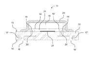
- FIG. 1 shows a cross-section of a basic example of a MEMS device package according to the present invention
- FIG. 2 shows cross-section of a MEMS device package with a cover structure comprising first and second coatings
- FIG. 3 shows a cross-section of a further development of the MEMS device package of FIG. 2 with electrically interconnected film of non-evaporable getter material.
- FIG. 1 shows an example of a basic MEMS systems device package 11 of the present invention.
- the package comprises the substrate 12 with a first substrate plane 13 and a second substrate plane 14 opposite to the first substrate plane.
- First and second connector pads 15 , 15 ′ are arranged on the first substrate plane and third and fourth connector pads 16 , 16 ′ are arranged on the second substrate plane.
- the substrate comprises a ceramic device with a stack of two ceramic layer and an electrode layer arranged between the ceramic layers.
- Vertical electrical connections 17 , 17 ′ go through the ceramic layers and electrically interconnect the connector pads on the first substrate plane with the electrode layers and the connector pads on the second substrate plane.
- the MEMS device 18 with a first and a second contact pad 19 , 19 ′ arranged on a front side of the MEMS device, is mounted in flip-chip technology on the first substrate plane so that the front side faces the first substrate plane.
- the first and second contact pad is electrically interconnected with the first and second connector pad.
- solder bumps 20 , 20 ′ can be used to complete the interconnect of the contact pads and the connector pads.
- An interspace 21 is present between the MEMS device and the first substrate plane.
- a film of non-evaporable getter material 22 is disposed at least partially in the interspace.
- the MEMS device is encapsulated between the substrate and a cover structure 23 arranged over and around the MEMS device and sealing to the first substrate plane 13 .
- FIG. 2 shows essentially the MEMS device package of FIG. 1 in a further embodiment wherein the cover structure comprises a first coating that is a polymer film 24 and a second coating 25 arranged over the polymer film.
- the polymer film seals to the first substrate plane 13 in a first periphery area 26 and encloses the MEMS device between the first substrate plane and the polymer film.
- the second coating 25 seals to the first substrate plane 13 in a second periphery area 27 and encloses the MEMS device between the first substrate plane 13 , the polymer film 24 and the second coating 25 .
- FIG. 3 shows a cross-section of a MEMS device package wherein the substrate 12 comprises fifth and sixth connector pads 28 , 28 ′ arranged on the first substrate plane 13 and seventh and eight connector pads 29 , 29 ′ arranged on the second substrate plane 14 , wherein the film of the non-evaporable getter material 22 is electrically interconnected with the fifth and sixth connector pad 28 , 28 ′ and through vertical electrical connections 30 , 30 ′ to the seventh and eighth connector pad 29 , 29 ′ arranged on the second substrate plane 14 .
- an electrical current can be selectively applied to the NEG film 22 in order to locally heat up the NEG film for activation without risk of thermal degradation of other components of the device package.
Landscapes
- Engineering & Computer Science (AREA)
- Microelectronics & Electronic Packaging (AREA)
- Manufacturing & Machinery (AREA)
- Computer Hardware Design (AREA)
- Physics & Mathematics (AREA)
- Acoustics & Sound (AREA)
- Micromachines (AREA)
- Surface Acoustic Wave Elements And Circuit Networks Thereof (AREA)
- Piezo-Electric Or Mechanical Vibrators, Or Delay Or Filter Circuits (AREA)
Abstract
Description
Claims (20)
Applications Claiming Priority (1)
| Application Number | Priority Date | Filing Date | Title |
|---|---|---|---|
| PCT/EP2013/060776 WO2014187505A1 (en) | 2013-05-24 | 2013-05-24 | Microelectromechanical systems device package and method for producing the microelectromechanical systems device package |
Publications (2)
| Publication Number | Publication Date |
|---|---|
| US20160049918A1 US20160049918A1 (en) | 2016-02-18 |
| US9479138B2 true US9479138B2 (en) | 2016-10-25 |
Family
ID=48699727
Family Applications (1)
| Application Number | Title | Priority Date | Filing Date |
|---|---|---|---|
| US14/784,351 Active US9479138B2 (en) | 2013-05-24 | 2013-05-24 | Microelectromechanical systems device package and method for producing the microelectromechanical systems device package |
Country Status (4)
| Country | Link |
|---|---|
| US (1) | US9479138B2 (en) |
| JP (1) | JP6193480B2 (en) |
| DE (1) | DE112013007109B4 (en) |
| WO (1) | WO2014187505A1 (en) |
Families Citing this family (7)
| Publication number | Priority date | Publication date | Assignee | Title |
|---|---|---|---|---|
| DE102014211333B4 (en) * | 2014-06-13 | 2025-11-06 | Robert Bosch Gmbh | Micromechanical component and method for its manufacture |
| US9718672B2 (en) * | 2015-05-27 | 2017-08-01 | Globalfoundries Singapore Pte. Ltd. | Electronic devices including substantially hermetically sealed cavities and getter films with Kelvin measurement arrangement for evaluating the getter films and methods for fabricating the same |
| DE102018104279B4 (en) * | 2018-02-26 | 2025-02-06 | Tdk Corporation | Electronic Device |
| CN108768335A (en) * | 2018-05-25 | 2018-11-06 | 张琴 | Air-tightness surface acoustic wave device encapsulating structure and production method |
| US11244876B2 (en) | 2019-10-09 | 2022-02-08 | Microchip Technology Inc. | Packaged semiconductor die with micro-cavity |
| CN111245385B (en) * | 2019-12-04 | 2025-03-14 | 天津大学 | Chip packaging module, packaging method and electronic device having the module |
| CN113651287A (en) * | 2021-07-01 | 2021-11-16 | 上海韦尔半导体股份有限公司 | Thin film sensor and packaging method thereof |
Citations (12)
| Publication number | Priority date | Publication date | Assignee | Title |
|---|---|---|---|---|
| JPH0229017A (en) | 1988-07-18 | 1990-01-31 | Mitsubishi Electric Corp | Packaging method for surface acoustic wave device |
| WO2004065289A2 (en) | 2003-01-17 | 2004-08-05 | Saes Getters S.P.A. | Micromechanical or microoptoelectronic devices with deposit of getter material and integrated heater, and support for the production thereof |
| WO2005076470A1 (en) | 2004-02-05 | 2005-08-18 | Epcos Ag | Electrical component and production method |
| WO2005113376A1 (en) | 2004-05-13 | 2005-12-01 | Honeywell International Inc. | Getter deposition for vacuum packaging |
| US20060131501A1 (en) | 2003-08-08 | 2006-06-22 | Matsushita Electric Industrial Co., Ltd. | Method for fabricating the same |
| CN102040186A (en) | 2010-11-09 | 2011-05-04 | 北京自动化控制设备研究所 | High vacuum ceramic LCC packaging method |
| US20110165718A1 (en) | 2004-02-12 | 2011-07-07 | Markus Lutz | Integrated getter area for wafer level encapsulated microelectromechanical systems |
| US20110290552A1 (en) | 2004-09-27 | 2011-12-01 | Qualcomm Mems Technologies, Inc. | Method and system for packaging mems devices with incorporated getter |
| EP2537797A1 (en) | 2011-06-23 | 2012-12-26 | Commissariat à l'Énergie Atomique et aux Énergies Alternatives | Structure with getter material hermetically protected during the manufacturing thereof |
| US8571239B2 (en) * | 2009-04-29 | 2013-10-29 | Epcos Ag | MEMS microphone |
| US8842859B2 (en) * | 2011-01-24 | 2014-09-23 | Invensense, Inc. | Packaged microphone with reduced parasitics |
| US9278854B2 (en) * | 2012-02-24 | 2016-03-08 | Epcos Ag | Method for producing a sensor |
Family Cites Families (8)
| Publication number | Priority date | Publication date | Assignee | Title |
|---|---|---|---|---|
| JPH10163798A (en) * | 1996-12-03 | 1998-06-19 | Semiconductors Niino:Kk | Surface acoustic wave element and electronic part using the same |
| JPH11326037A (en) | 1998-05-12 | 1999-11-26 | Mitsubishi Electric Corp | Vacuum package for infrared detector and method of manufacturing the same |
| DE10238523B4 (en) | 2002-08-22 | 2014-10-02 | Epcos Ag | Encapsulated electronic component and method of manufacture |
| WO2006124597A2 (en) | 2005-05-12 | 2006-11-23 | Foster Ron B | Infinitely stackable interconnect device and method |
| DE102005050398A1 (en) * | 2005-10-20 | 2007-04-26 | Epcos Ag | Cavity housing for a mechanically sensitive electronic device and method of manufacture |
| US20070114643A1 (en) | 2005-11-22 | 2007-05-24 | Honeywell International Inc. | Mems flip-chip packaging |
| DE102007028288B4 (en) * | 2007-06-20 | 2013-06-06 | Epcos Ag | Acoustic wave MEMS device and method of manufacture |
| JP2011211439A (en) * | 2010-03-29 | 2011-10-20 | Seiko Instruments Inc | Method of manufacturing silicon bonding film, method of manufacturing package, package, piezoelectric oscillator, oscillator, electronic device, and electric wave clock |
-
2013
- 2013-05-24 JP JP2016514278A patent/JP6193480B2/en active Active
- 2013-05-24 DE DE112013007109.6T patent/DE112013007109B4/en active Active
- 2013-05-24 WO PCT/EP2013/060776 patent/WO2014187505A1/en not_active Ceased
- 2013-05-24 US US14/784,351 patent/US9479138B2/en active Active
Patent Citations (14)
| Publication number | Priority date | Publication date | Assignee | Title |
|---|---|---|---|---|
| JPH0229017A (en) | 1988-07-18 | 1990-01-31 | Mitsubishi Electric Corp | Packaging method for surface acoustic wave device |
| WO2004065289A2 (en) | 2003-01-17 | 2004-08-05 | Saes Getters S.P.A. | Micromechanical or microoptoelectronic devices with deposit of getter material and integrated heater, and support for the production thereof |
| US20060131501A1 (en) | 2003-08-08 | 2006-06-22 | Matsushita Electric Industrial Co., Ltd. | Method for fabricating the same |
| WO2005076470A1 (en) | 2004-02-05 | 2005-08-18 | Epcos Ag | Electrical component and production method |
| US7868448B2 (en) | 2004-02-05 | 2011-01-11 | Epcos Ag | Electrical component and production thereof |
| US20110165718A1 (en) | 2004-02-12 | 2011-07-07 | Markus Lutz | Integrated getter area for wafer level encapsulated microelectromechanical systems |
| WO2005113376A1 (en) | 2004-05-13 | 2005-12-01 | Honeywell International Inc. | Getter deposition for vacuum packaging |
| US20110290552A1 (en) | 2004-09-27 | 2011-12-01 | Qualcomm Mems Technologies, Inc. | Method and system for packaging mems devices with incorporated getter |
| US8571239B2 (en) * | 2009-04-29 | 2013-10-29 | Epcos Ag | MEMS microphone |
| CN102040186A (en) | 2010-11-09 | 2011-05-04 | 北京自动化控制设备研究所 | High vacuum ceramic LCC packaging method |
| US8842859B2 (en) * | 2011-01-24 | 2014-09-23 | Invensense, Inc. | Packaged microphone with reduced parasitics |
| US20120328779A1 (en) | 2011-06-23 | 2012-12-27 | Commissariat A L'energie Atomique Et Aux Ene Alt | Structure made of getter material hermetically protected during manufacturing |
| EP2537797A1 (en) | 2011-06-23 | 2012-12-26 | Commissariat à l'Énergie Atomique et aux Énergies Alternatives | Structure with getter material hermetically protected during the manufacturing thereof |
| US9278854B2 (en) * | 2012-02-24 | 2016-03-08 | Epcos Ag | Method for producing a sensor |
Also Published As
| Publication number | Publication date |
|---|---|
| DE112013007109T5 (en) | 2016-04-07 |
| WO2014187505A1 (en) | 2014-11-27 |
| JP2016525946A (en) | 2016-09-01 |
| DE112013007109B4 (en) | 2023-03-16 |
| US20160049918A1 (en) | 2016-02-18 |
| JP6193480B2 (en) | 2017-09-06 |
Similar Documents
| Publication | Publication Date | Title |
|---|---|---|
| US9479138B2 (en) | Microelectromechanical systems device package and method for producing the microelectromechanical systems device package | |
| JP5763682B2 (en) | Miniaturized electrical device including MEMS and ASIC and method for manufacturing the same | |
| JP6974685B2 (en) | Structures and methods for packaging MEMS susceptible to stress | |
| US6323550B1 (en) | Package for sealing an integrated circuit die | |
| US8520396B2 (en) | Method for producing an electronic module | |
| US8169041B2 (en) | MEMS package and method for the production thereof | |
| JP5894186B2 (en) | Packaged electronic devices | |
| US7605466B2 (en) | Sealed wafer packaging of microelectromechanical systems | |
| US9533875B2 (en) | MEMS sensor packaging and method thereof | |
| US20110156106A1 (en) | Hermetic mems device and method for fabricating hermetic mems device and package structure of mems device | |
| WO2004051744A2 (en) | Mems control chip integration | |
| US20050269678A1 (en) | Package for sealing an integrated circuit die | |
| US20170008760A1 (en) | Mems-cmos-mems platform | |
| TW201307183A (en) | Thin metal shield on electronic devices | |
| US8884331B2 (en) | Structure for hermetic encapsulation of a device and an electronic component | |
| US20080308922A1 (en) | Method for packaging semiconductors at a wafer level | |
| CN110606465A (en) | Method and system for manufacturing a system comprising first and second microelectromechanical elements | |
| JP2008182014A (en) | Package substrate and manufacturing method thereof | |
| US20100237489A1 (en) | Structure and Method for Sealing Cavity of Micro-Electro-Mechanical Device | |
| JP2004296724A (en) | Electronic component sealing substrate and method of manufacturing electronic device using the same | |
| US20080122073A1 (en) | MEMS module package | |
| JP4903540B2 (en) | Substrate for encapsulating microelectromechanical components, substrate for encapsulating microelectromechanical components in plural shapes, microelectromechanical device, and manufacturing method of microelectronic mechanical device | |
| JP5606696B2 (en) | Mechanical quantity sensor and manufacturing method thereof | |
| KR20130136440A (en) | Module and production method | |
| JP2008147368A (en) | Semiconductor device |
Legal Events
| Date | Code | Title | Description |
|---|---|---|---|
| AS | Assignment |
Owner name: EPCOS AG, GERMANY Free format text: ASSIGNMENT OF ASSIGNORS INTEREST;ASSIGNOR:MOULARD, GILLES, DR.;REEL/FRAME:037563/0878 Effective date: 20151120 |
|
| STCF | Information on status: patent grant |
Free format text: PATENTED CASE |
|
| AS | Assignment |
Owner name: SNAPTRACK, INC., CALIFORNIA Free format text: ASSIGNMENT OF ASSIGNORS INTEREST;ASSIGNOR:EPCOS AG;REEL/FRAME:041608/0145 Effective date: 20170201 |
|
| MAFP | Maintenance fee payment |
Free format text: PAYMENT OF MAINTENANCE FEE, 4TH YEAR, LARGE ENTITY (ORIGINAL EVENT CODE: M1551); ENTITY STATUS OF PATENT OWNER: LARGE ENTITY Year of fee payment: 4 |
|
| MAFP | Maintenance fee payment |
Free format text: PAYMENT OF MAINTENANCE FEE, 8TH YEAR, LARGE ENTITY (ORIGINAL EVENT CODE: M1552); ENTITY STATUS OF PATENT OWNER: LARGE ENTITY Year of fee payment: 8 |