US9478944B2 - Semiconductor laser element and method of manufacturing semiconductor laser element - Google Patents
Semiconductor laser element and method of manufacturing semiconductor laser element Download PDFInfo
- Publication number
- US9478944B2 US9478944B2 US14/460,090 US201414460090A US9478944B2 US 9478944 B2 US9478944 B2 US 9478944B2 US 201414460090 A US201414460090 A US 201414460090A US 9478944 B2 US9478944 B2 US 9478944B2
- Authority
- US
- United States
- Prior art keywords
- layer
- semiconductor laser
- laser element
- window region
- active layer
- Prior art date
- Legal status (The legal status is an assumption and is not a legal conclusion. Google has not performed a legal analysis and makes no representation as to the accuracy of the status listed.)
- Active
Links
- 239000004065 semiconductor Substances 0.000 title claims abstract description 157
- 238000004519 manufacturing process Methods 0.000 title description 16
- 238000009792 diffusion process Methods 0.000 claims abstract description 47
- 239000011701 zinc Substances 0.000 claims description 77
- 238000005253 cladding Methods 0.000 claims description 65
- 239000012535 impurity Substances 0.000 claims description 58
- 229910001218 Gallium arsenide Inorganic materials 0.000 claims description 28
- 238000007669 thermal treatment Methods 0.000 claims description 25
- 229910052725 zinc Inorganic materials 0.000 claims description 10
- HCHKCACWOHOZIP-UHFFFAOYSA-N Zinc Chemical compound [Zn] HCHKCACWOHOZIP-UHFFFAOYSA-N 0.000 claims description 8
- 229910052799 carbon Inorganic materials 0.000 claims description 7
- OKTJSMMVPCPJKN-UHFFFAOYSA-N Carbon Chemical group [C] OKTJSMMVPCPJKN-UHFFFAOYSA-N 0.000 claims description 6
- 239000002019 doping agent Substances 0.000 claims 1
- 230000001737 promoting effect Effects 0.000 abstract description 46
- 239000010408 film Substances 0.000 description 91
- 238000004151 rapid thermal annealing Methods 0.000 description 38
- 230000001629 suppression Effects 0.000 description 27
- 230000004888 barrier function Effects 0.000 description 19
- 238000000034 method Methods 0.000 description 18
- 239000000203 mixture Substances 0.000 description 14
- 238000007796 conventional method Methods 0.000 description 13
- 238000010586 diagram Methods 0.000 description 13
- 239000000463 material Substances 0.000 description 11
- VYPSYNLAJGMNEJ-UHFFFAOYSA-N Silicium dioxide Chemical compound O=[Si]=O VYPSYNLAJGMNEJ-UHFFFAOYSA-N 0.000 description 10
- 238000005530 etching Methods 0.000 description 10
- 230000010355 oscillation Effects 0.000 description 10
- 230000008859 change Effects 0.000 description 9
- 239000000758 substrate Substances 0.000 description 9
- 229910004205 SiNX Inorganic materials 0.000 description 8
- 230000001419 dependent effect Effects 0.000 description 8
- 230000031700 light absorption Effects 0.000 description 8
- 230000003287 optical effect Effects 0.000 description 8
- 238000010521 absorption reaction Methods 0.000 description 7
- 230000007423 decrease Effects 0.000 description 6
- 230000015556 catabolic process Effects 0.000 description 5
- 229910052681 coesite Inorganic materials 0.000 description 5
- 229910052906 cristobalite Inorganic materials 0.000 description 5
- 239000013078 crystal Substances 0.000 description 5
- 230000007547 defect Effects 0.000 description 5
- 238000006731 degradation reaction Methods 0.000 description 5
- 230000008569 process Effects 0.000 description 5
- 239000000377 silicon dioxide Substances 0.000 description 5
- 229910052682 stishovite Inorganic materials 0.000 description 5
- 229910052905 tridymite Inorganic materials 0.000 description 5
- QGZKDVFQNNGYKY-UHFFFAOYSA-N Ammonia Chemical compound N QGZKDVFQNNGYKY-UHFFFAOYSA-N 0.000 description 4
- 230000015572 biosynthetic process Effects 0.000 description 4
- 239000000969 carrier Substances 0.000 description 4
- 238000004140 cleaning Methods 0.000 description 4
- 230000006378 damage Effects 0.000 description 4
- 238000000206 photolithography Methods 0.000 description 4
- 229910000980 Aluminium gallium arsenide Inorganic materials 0.000 description 3
- 239000000370 acceptor Substances 0.000 description 3
- 238000004050 hot filament vapor deposition Methods 0.000 description 3
- 238000009413 insulation Methods 0.000 description 3
- 238000012360 testing method Methods 0.000 description 3
- 230000032683 aging Effects 0.000 description 2
- 229910021529 ammonia Inorganic materials 0.000 description 2
- 150000001875 compounds Chemical class 0.000 description 2
- 230000003247 decreasing effect Effects 0.000 description 2
- 230000001687 destabilization Effects 0.000 description 2
- 238000012986 modification Methods 0.000 description 2
- 230000004048 modification Effects 0.000 description 2
- 230000006798 recombination Effects 0.000 description 2
- 238000005215 recombination Methods 0.000 description 2
- VZGDMQKNWNREIO-UHFFFAOYSA-N tetrachloromethane Chemical compound ClC(Cl)(Cl)Cl VZGDMQKNWNREIO-UHFFFAOYSA-N 0.000 description 2
- 229910000530 Gallium indium arsenide Inorganic materials 0.000 description 1
- BLRPTPMANUNPDV-UHFFFAOYSA-N Silane Chemical compound [SiH4] BLRPTPMANUNPDV-UHFFFAOYSA-N 0.000 description 1
- 208000034841 Thrombotic Microangiopathies Diseases 0.000 description 1
- RBFQJDQYXXHULB-UHFFFAOYSA-N arsane Chemical compound [AsH3] RBFQJDQYXXHULB-UHFFFAOYSA-N 0.000 description 1
- 150000001721 carbon Chemical class 0.000 description 1
- 238000005229 chemical vapour deposition Methods 0.000 description 1
- 230000000593 degrading effect Effects 0.000 description 1
- 238000000151 deposition Methods 0.000 description 1
- 238000009826 distribution Methods 0.000 description 1
- 229910021478 group 5 element Inorganic materials 0.000 description 1
- 238000005259 measurement Methods 0.000 description 1
- 125000002524 organometallic group Chemical group 0.000 description 1
- 238000007254 oxidation reaction Methods 0.000 description 1
- 239000002994 raw material Substances 0.000 description 1
- 238000004904 shortening Methods 0.000 description 1
- 229910000077 silane Inorganic materials 0.000 description 1
- HJUGFYREWKUQJT-UHFFFAOYSA-N tetrabromomethane Chemical compound BrC(Br)(Br)Br HJUGFYREWKUQJT-UHFFFAOYSA-N 0.000 description 1
- 239000010409 thin film Substances 0.000 description 1
Images


Classifications
-
- H—ELECTRICITY
- H01—ELECTRIC ELEMENTS
- H01S—DEVICES USING THE PROCESS OF LIGHT AMPLIFICATION BY STIMULATED EMISSION OF RADIATION [LASER] TO AMPLIFY OR GENERATE LIGHT; DEVICES USING STIMULATED EMISSION OF ELECTROMAGNETIC RADIATION IN WAVE RANGES OTHER THAN OPTICAL
- H01S5/00—Semiconductor lasers
- H01S5/10—Construction or shape of the optical resonator, e.g. extended or external cavity, coupled cavities, bent-guide, varying width, thickness or composition of the active region
- H01S5/16—Window-type lasers, i.e. with a region of non-absorbing material between the active region and the reflecting surface
- H01S5/164—Window-type lasers, i.e. with a region of non-absorbing material between the active region and the reflecting surface with window regions comprising semiconductor material with a wider bandgap than the active layer
-
- H—ELECTRICITY
- H01—ELECTRIC ELEMENTS
- H01S—DEVICES USING THE PROCESS OF LIGHT AMPLIFICATION BY STIMULATED EMISSION OF RADIATION [LASER] TO AMPLIFY OR GENERATE LIGHT; DEVICES USING STIMULATED EMISSION OF ELECTROMAGNETIC RADIATION IN WAVE RANGES OTHER THAN OPTICAL
- H01S5/00—Semiconductor lasers
- H01S5/04—Processes or apparatus for excitation, e.g. pumping, e.g. by electron beams
- H01S5/042—Electrical excitation ; Circuits therefor
- H01S5/0421—Electrical excitation ; Circuits therefor characterised by the semiconducting contacting layers
-
- H—ELECTRICITY
- H01—ELECTRIC ELEMENTS
- H01S—DEVICES USING THE PROCESS OF LIGHT AMPLIFICATION BY STIMULATED EMISSION OF RADIATION [LASER] TO AMPLIFY OR GENERATE LIGHT; DEVICES USING STIMULATED EMISSION OF ELECTROMAGNETIC RADIATION IN WAVE RANGES OTHER THAN OPTICAL
- H01S5/00—Semiconductor lasers
- H01S5/10—Construction or shape of the optical resonator, e.g. extended or external cavity, coupled cavities, bent-guide, varying width, thickness or composition of the active region
- H01S5/16—Window-type lasers, i.e. with a region of non-absorbing material between the active region and the reflecting surface
- H01S5/162—Window-type lasers, i.e. with a region of non-absorbing material between the active region and the reflecting surface with window regions made by diffusion or disordening of the active layer
-
- H—ELECTRICITY
- H01—ELECTRIC ELEMENTS
- H01S—DEVICES USING THE PROCESS OF LIGHT AMPLIFICATION BY STIMULATED EMISSION OF RADIATION [LASER] TO AMPLIFY OR GENERATE LIGHT; DEVICES USING STIMULATED EMISSION OF ELECTROMAGNETIC RADIATION IN WAVE RANGES OTHER THAN OPTICAL
- H01S5/00—Semiconductor lasers
- H01S5/10—Construction or shape of the optical resonator, e.g. extended or external cavity, coupled cavities, bent-guide, varying width, thickness or composition of the active region
- H01S5/16—Window-type lasers, i.e. with a region of non-absorbing material between the active region and the reflecting surface
- H01S5/168—Window-type lasers, i.e. with a region of non-absorbing material between the active region and the reflecting surface with window regions comprising current blocking layers
-
- H—ELECTRICITY
- H01—ELECTRIC ELEMENTS
- H01S—DEVICES USING THE PROCESS OF LIGHT AMPLIFICATION BY STIMULATED EMISSION OF RADIATION [LASER] TO AMPLIFY OR GENERATE LIGHT; DEVICES USING STIMULATED EMISSION OF ELECTROMAGNETIC RADIATION IN WAVE RANGES OTHER THAN OPTICAL
- H01S5/00—Semiconductor lasers
- H01S5/20—Structure or shape of the semiconductor body to guide the optical wave ; Confining structures perpendicular to the optical axis, e.g. index or gain guiding, stripe geometry, broad area lasers, gain tailoring, transverse or lateral reflectors, special cladding structures, MQW barrier reflection layers
- H01S5/2054—Methods of obtaining the confinement
- H01S5/2059—Methods of obtaining the confinement by means of particular conductivity zones, e.g. obtained by particle bombardment or diffusion
- H01S5/2072—Methods of obtaining the confinement by means of particular conductivity zones, e.g. obtained by particle bombardment or diffusion obtained by vacancy induced diffusion
-
- H—ELECTRICITY
- H01—ELECTRIC ELEMENTS
- H01S—DEVICES USING THE PROCESS OF LIGHT AMPLIFICATION BY STIMULATED EMISSION OF RADIATION [LASER] TO AMPLIFY OR GENERATE LIGHT; DEVICES USING STIMULATED EMISSION OF ELECTROMAGNETIC RADIATION IN WAVE RANGES OTHER THAN OPTICAL
- H01S5/00—Semiconductor lasers
- H01S5/30—Structure or shape of the active region; Materials used for the active region
- H01S5/305—Structure or shape of the active region; Materials used for the active region characterised by the doping materials used in the laser structure
- H01S5/3054—Structure or shape of the active region; Materials used for the active region characterised by the doping materials used in the laser structure p-doping
-
- H—ELECTRICITY
- H01—ELECTRIC ELEMENTS
- H01S—DEVICES USING THE PROCESS OF LIGHT AMPLIFICATION BY STIMULATED EMISSION OF RADIATION [LASER] TO AMPLIFY OR GENERATE LIGHT; DEVICES USING STIMULATED EMISSION OF ELECTROMAGNETIC RADIATION IN WAVE RANGES OTHER THAN OPTICAL
- H01S5/00—Semiconductor lasers
- H01S5/30—Structure or shape of the active region; Materials used for the active region
- H01S5/32—Structure or shape of the active region; Materials used for the active region comprising PN junctions, e.g. hetero- or double- heterostructures
- H01S5/3223—IV compounds
-
- H—ELECTRICITY
- H01—ELECTRIC ELEMENTS
- H01S—DEVICES USING THE PROCESS OF LIGHT AMPLIFICATION BY STIMULATED EMISSION OF RADIATION [LASER] TO AMPLIFY OR GENERATE LIGHT; DEVICES USING STIMULATED EMISSION OF ELECTROMAGNETIC RADIATION IN WAVE RANGES OTHER THAN OPTICAL
- H01S5/00—Semiconductor lasers
- H01S5/30—Structure or shape of the active region; Materials used for the active region
- H01S5/34—Structure or shape of the active region; Materials used for the active region comprising quantum well or superlattice structures, e.g. single quantum well [SQW] lasers, multiple quantum well [MQW] lasers or graded index separate confinement heterostructure [GRINSCH] lasers
- H01S5/3427—Structure or shape of the active region; Materials used for the active region comprising quantum well or superlattice structures, e.g. single quantum well [SQW] lasers, multiple quantum well [MQW] lasers or graded index separate confinement heterostructure [GRINSCH] lasers in IV compounds
Definitions
- the present invention relates to a semiconductor laser element including a window region with a disordered portion formed by diffusion of group-III vacancies, and a non-window region with an active layer of a quantum well structure, where a promoting film that absorbs a predetermined atom to promote the diffusion of the group-III vacancies is provided on the window region to form the disordered portion, and to a method of manufacturing the semiconductor laser element.
- the window region disordered using the IFVD method may absorb laser light of a wavelength corresponding to higher-order energy oscillation. Therefore, there has been a problem that, when the semiconductor laser element is driven under severe conditions, the semiconductor laser element is degraded due to COD, and a highly reliable semiconductor laser element is not obtainable.
- a semiconductor laser element includes: a window region including a disordered portion formed by diffusion of a group-III vacancy, the diffusion promoted by providing on the window region a promoting film that absorbs a predetermined atom; a non-window region including an active layer of a quantum well structure; and a difference equal to or larger than 50 meV between an energy band gap in the window region and an energy band gap in the non-window region.
- a semiconductor laser element includes: a window region including a disordered portion formed by diffusion of a group-III vacancy, the diffusion promoted by providing on the window region a promoting film that absorbs a predetermined atom; a non-window region including an active layer of a quantum well structure; and a layer near the active layer, the layer being doped with an impurity that preferentially substitutes a group-V site.
- a manufacturing method, according to still another aspect of the present invention, for a semiconductor laser element including a window region with a disordered portion formed by diffusion of a group-III vacancy and a non-window region including an active layer of a quantum well structure includes: forming on the window region a promoting film that absorbs a predetermined atom and promotes the diffusion of the group-III vacancy; and forming, near the active layer, a layer doped with an impurity that preferentially substitutes a group-V site.
- FIG. 1 is a perspective view of a semiconductor laser element according to a first embodiment
- FIG. 2 is a cross section of the semiconductor laser element depicted in FIG. 1 ;
- FIG. 3 is a longitudinal section of the semiconductor laser element depicted in FIG. 1 ;
- FIG. 4 is an explanatory diagram for a manufacturing method of the semiconductor laser element according to the first embodiment
- FIG. 5 is an explanatory diagram for the manufacturing method of the semiconductor laser element according to the first embodiment
- FIG. 6 is an explanatory diagram for the manufacturing method of the semiconductor laser element according to the first embodiment
- FIG. 7 is an explanatory diagram for the manufacturing method of the semiconductor laser element according to the first embodiment.
- FIG. 8 is an explanatory diagram for the manufacturing method of the semiconductor laser element according to the first embodiment
- FIG. 9 is an explanatory diagram for diffusion of vacancies and interstitial Zn in a semiconductor laser element according to a conventional technique
- FIG. 10 depicts wavelength changes of light absorption amounts in a window region and a non-window region of the semiconductor laser element according to the conventional technique
- FIG. 11 depicts time dependency of a change in laser light intensity of the semiconductor laser element according to the conventional technique
- FIG. 12 is an explanatory diagram for diffusion of vacancies and C in the semiconductor laser element according to the first embodiment
- FIG. 13 depicts wavelength changes of light absorption amounts in a window region and a non-window region of the semiconductor laser element according to the first embodiment
- FIG. 14 depicts a relationship between thermal treatment temperatures of RTA and energy shift amounts in the window region and the non-window region of the semiconductor laser element according to the first embodiment
- FIG. 15 depicts light output characteristics upon pulse driving of the semiconductor laser according to the first embodiment
- FIG. 16 depicts ageing test results of the semiconductor laser according to the first embodiment
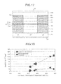
- FIG. 17 is another example of a cross section of the semiconductor laser element according to the first embodiment.
- FIG. 18 depicts a relationship between thermal treatment temperatures of RTA and energy shift amounts in a window region and a non-window region of the semiconductor laser element depicted in FIG. 17 ;
- FIG. 19 is an explanatory diagram for a manufacturing method of the semiconductor laser element depicted in FIG. 17 ;
- FIG. 20 is an explanatory diagram for the manufacturing method of the semiconductor laser element depicted in FIG. 17 ;
- FIG. 21 is an explanatory diagram for the manufacturing method of the semiconductor laser element depicted in FIG. 17 ;
- FIG. 22 is an explanatory diagram for the manufacturing method of the semiconductor laser element depicted in FIG. 17 ;
- FIG. 23 is an explanatory diagram for the manufacturing method of the semiconductor laser element depicted in FIG. 17 ;
- FIG. 24 is another example of a cross section of the semiconductor laser element according to the first embodiment.
- FIG. 25 is a cross section of a semiconductor laser element according to a second embodiment
- FIG. 26 is an explanatory diagram for a state of a regrowth interface in the semiconductor laser element depicted in FIG. 17 ;
- FIG. 27 depicts a relationship between thermal treatment temperatures of RTA and energy shift amounts in a window region and a non-window region of the semiconductor laser element depicted in FIG. 25 ;
- FIG. 28 depicts a relationship between distances of C from an active layer in the first embodiment, Zn from an active layer in the second embodiment, and Zn from an active layer in the conventional technique, and doping concentrations of these impurities;
- FIG. 29 is another example of a cross section of the semiconductor laser element according to the second embodiment.
- FIG. 30 is another example of a cross section of the semiconductor laser element according to the second embodiment.
- FIG. 31 is another example of a cross section of the semiconductor laser element according to the second embodiment.
- FIG. 32 is another example of a cross section of the semiconductor laser element according to the second embodiment.
- FIG. 33 is another example of a cross section of the semiconductor laser element according to the first and second embodiments.
- FIG. 1 is a perspective view of the semiconductor laser element according to the first embodiment.
- FIG. 2 is a cross section of the semiconductor laser element depicted in FIG. 1 .
- FIG. 3 is a longitudinal cross section of the semiconductor laser element depicted in FIG. 1 .
- a semiconductor laser element 1 has a ridge structure constricting a current in a striped form, has a high reflection film 2 formed at a reflection end of laser light 4 , and has a low reflection film 3 formed at an exit end of the laser light. Laser light generated inside the semiconductor laser element 1 and laser light reflected at the high reflection film 2 are transmitted through the low reflection film 3 , and are emitted to the outside.
- FIG. 2 and FIG. 3 A structure of the semiconductor laser element 1 depicted in FIG. 1 is explained next with reference to FIG. 2 and FIG. 3 .
- an n-buffer layer 12 , an n-cladding layer 13 , an n-guide layer 14 , an active layer 15 , a p-guide layer 16 , a p-cladding layer 17 , a p-contact layer 18 , and an insulation layer 19 are sequentially stacked on a substrate 11 , which is an n-GaAs substrate.
- the semiconductor laser element 1 has an upper electrode 20 formed above the p-contact layer 18 and a lower electrode 21 formed below the substrate 11 .
- An impurity which is C, is doped into the p-guide layer 16 formed on a side of stacking a p-type cladding, that is, above the active layer 15 , into the p-cladding layer 17 formed on the side of stacking the p-type cladding with respect to the active layer 15 , and into the p-contact layer 18 formed to inject the positive hole into the active layer 15 .
- the semiconductor laser element 1 has a ridge structure constricting in a striped form a current injected into the active layer 15 , and functioning as an optical waveguide along the stripe.
- the semiconductor laser element 1 is processed in a mesa form in which a width of a layer region including an upper part of the p-cladding layer 17 plus the p-contact layer 18 is narrowed down in a direction perpendicular to a laser-light emission direction.
- a window region 23 that absorbs less laser light than a non-window region 24 is provided at a light-emitting facet of the semiconductor laser element 1 .
- the window region 23 includes a disordered portion formed by diffusion of group-III vacancies, and the non-window region 24 has the active layer 15 of a quantum well structure and does not include the disordered portion.
- an energy band gap in the window region 23 is increased such that its difference from an energy band gap in the non-window region 24 becomes equal to or greater than 50 meV to suppress absorption of laser light and prevent COD.
- the substrate 11 is made of a material including n-GaAs.
- the n-buffer layer 12 is a buffer layer necessary for growing a stacked structure of high-quality epitaxial layers on the substrate 11 , and is made of a layer material including n-GaAs.
- the n-cladding layer 13 and the n-guide layer 14 have refractive indices and thicknesses, which are determined to achieve an arbitrary optical confinement state with respect to a stacking direction, and are made of materials including n-AlGaAs.
- an Al composition in the n-guide layer 14 is equal to or greater than 20% and less than 40%.
- An Al composition in the n-cladding layer 13 is usually set greater than the Al composition in the n-guide layer 14 to decrease its refractive index.
- a film thickness of the n-guide layer 14 is preferably equal to or larger than 200 nanometers, for example, about 400 nanometers.
- a thickness of the n-cladding layer 13 is preferably equal to or larger than 1 micrometer, and may be about 3 micrometers.
- An intentionally not-doped high-purity layer may be used as the n-guide layer 14 , but if a thickness of the n-guide layer 14 is set equal to or larger than 100 nanometers, influence by a residual impurity is large, and thus doping is preferably performed.
- the active layer 15 includes a lower barrier layer 15 a , a quantum well layer 15 b , and an upper barrier layer 15 c .
- the lower barrier layer 15 a and the upper barrier layer 15 c have a function of a barrier that confines carriers in the quantum well layer 15 b , and are made of materials including intentionally not-doped high-purity AlGaAs.
- the quantum well layer 15 b is made of a material including intentionally not-doped high-purity InGaAs.
- Light-emission recombined energy of the confined carriers is determined by a structure of a potential well determined by an In composition and a film thickness of the quantum well layer 15 b and compositions of the lower barrier layer 15 a and the upper barrier layer 15 c .
- a structure of a single quantum well layer (SQW) has been explained above, a structure of a multi-quantum well layer (MQW) with the quantum well layer 15 b , the lower barrier layer 15 a , and the upper barrier layer 15 c stacked repeatedly by a predetermined number of times may be provided.
- a structure of an intentionally not-doped high-purity layer has been explained above, donors and acceptors may be intentionally added to the quantum well layer 15 b , the lower barrier layer 15 a , and the upper barrier layer 15 c .
- the lower barrier layer 15 a and the n-guide layer 14 may have a same composition
- the upper barrier layer 15 c and the p-guide layer 16 may have a same composition
- the lower barrier layer 15 a and the upper barrier layer 15 c are not necessarily structured.
- the p-guide layer 16 and the p-cladding layer 17 are made of materials including p-AlGaAs.
- An Al composition of the p-guide layer 16 is generally equal to or greater than 20%, and is preferably equal to or greater than 30%. This is to increase an energy shift in the window region 23 , which is a change in an energy band gap due to disordering, and to perform highly selective disordering in the window region 23 adequately.
- An Al composition in the p-cladding layer 17 is usually 40% to 50%. To decrease a waveguide loss by shifting an optical field in the layer towards the n-cladding layer 13 , the Al composition in the p-cladding layer 17 is set a little greater than that in the n-cladding layer 13 . An Al composition in the p-guide layer 16 is set smaller than the Al composition in the p-cladding layer 17 .
- a film thickness of the p-guide layer 16 is preferably equal to or larger than 200 nanometers, for example, about 400 nanometers.
- a thickness of the p-cladding layer 17 is preferably around 1 to 2 micrometers.
- An intentionally not-doped high-purity layer may be used as the p-guide layer 16 , but if a thickness of the guide layer is set equal to or larger than 100 nanometers, influence by conductivity variation due to a residual impurity is large, and thus to increase manufacture reproducibility, intentional doping is preferably performed.
- Carbon (C) is doped as an acceptor impurity, into the p-cladding layer 17 and the p-guide layer 16 .
- Concentration of C in the p-guide layer 16 is set to 0.1 to 1.0 ⁇ 10 17 cm ⁇ 3 , and is preferably about 0.5 to 1.0 ⁇ 10 17 cm ⁇ 3 .
- In the p-cladding layer 17 it is set equal to or higher than 1.0 ⁇ 10 17 cm ⁇ 3 .
- the p-contact layer 18 is for making the p-cladding layer 17 come in Ohmic contact with the upper electrode 20 .
- the p-contact layer 18 is made of a layer material including p-GaAs. A high concentration of C is doped into the p-contact layer 18 , thereby achieving the Ohmic contact.
- a manufacturing method of the semiconductor laser element 1 is explained next with reference to FIG. 4 to FIG. 8 .
- the n-buffer layer 12 , the n-cladding layer 13 , the n-guide layer 14 , the active layer 15 , the p-guide layer 16 , the p-cladding layer 17 , and the p-contact layer 18 are formed on the substrate 11 by epitaxial growth.
- Carbon (C) is doped as an impurity in the p-guide layer 16 , the p-cladding layer 17 , and the p-contact layer 18 .
- SiN x is deposited on the p-contact layer 18 by using a catalytic chemical vapor deposition (CVD) method.
- This SiN x film has a higher proportion of N than the stoichiometric composition, and is formed in a state in which flow rates of silane and ammonia, which are the raw materials, are adjusted to be ammonia rich.
- SiN x in a region other than a region corresponding to the window region 23 is removed by performing photolithography and etching, thereby forming a promoting film 25 as depicted in FIG. 5 . Because the promoting film 25 is a film formed of SiN x in an N-rich condition, it is a sparse film.
- the promoting film 25 needs to be formed to include a facet from which laser light is emitted.
- the promoting film 25 is formed in a latticed form and a striped form on a plane of the semiconductor laser element 1 , to cover the active layer 15 when viewed from a laser-light emission side.
- 30 nanometers, for example, of a SiN x film formed in a Si-rich condition is deposited on the p-contact layer 18 and the promoting film 25 by using the catalytic CVD method, thereby forming a suppression film 26 .
- This SiN x has a higher proportion of Si than the stoichiometric composition. Because the suppression film 26 is formed by the catalytic CVD method, it becomes a dense film.
- the promoting film 25 may be formed after a SiN x film for forming a suppression film 26 is formed and the SiN x corresponding to the window region 23 is removed to form the suppression film 26 .
- Rapid thermal annealing is performed next for 30 seconds at 915° C., for example.
- the promoting film 25 is a sparse film, the film is able to absorb diffused Ga. Therefore, the promoting film 25 absorbs Ga in each layer positioned below the promoting film 25 by the RTA. Vacancies are generated on a surface of the p-contact layer 18 contacting the promoting film 25 below the promoting film 25 , and the vacancies are diffused to the active layer 15 .
- the quantum well layer 15 b positioned below the promoting film 25 is disordered, thereby forming the window region 23 as depicted in FIG. 6 .
- the promoting film 25 has a function of promoting disordering in the window region 23 by absorbing Ga and promoting the diffusion of vacancies.
- the suppression film 26 is formed to contact the p-contact layer 18 in a region where the promoting film 25 is not formed. Because the suppression film 26 is a dense film, it does not absorb Ga, and suppresses diffusion of Ga. As a result, in the region where the promoting film 25 is not formed, vacancies are not generated, disordering thus does not occur, and this region becomes the non-window region 24 that does not include the disordered portion.
- the suppression film 26 thus has a function of suppressing disordering in the non-window region 24 .
- the p-contact layer 18 other than a region contacting the upper electrode 20 and an upper portion of the p-cladding layer 17 are removed to form a ridge structure, by performing photolithography and etching, as depicted in FIG. 7 .
- the insulation layer 19 is formed, the insulation layer 19 other than a region contacting the upper electrode 20 is removed, by performing photolithography and etching, as depicted in FIG. 8 .
- a semiconductor wafer is cleaved, and the high reflection film 2 and the low reflection film 3 are formed on the cleaved surfaces, and each semiconductor laser elements 1 is cut out, thereby forming finally the semiconductor laser element 1 .
- C is doped as an impurity into the p-guide layer 16 which is a layer close to the active layer 15 , and the p-cladding layer 17 and the p-contact layer 18 , which are layers above the p-guide layer 16 .
- Zn that preferentially substitutes a group-III site as an impurity is doped into a p-guide layer 116 , a p-cladding layer 117 , and a p-contact layer 118 .
- Zinc has a large diffusion coefficient and high impurity diffusion performance, and easily generates interstitial atoms, and the generated interstitial atoms have a high diffusion velocity.
- a group-III vacancy 31 a generated by diffusion of Ga occupying the group-III reaches the active layer 15 to form a window region as indicated by an arrow Y 0 in FIG. 9 .
- an interstitial Zn 30 b generated may recombine with a group-III vacancy 31 b as indicated by an arrow Y 2 in FIG. 9 .
- the interstitial Zn 30 b and the group-III vacancy 31 b are both of group-III, they tend to be recombined easily.
- Zn easily generates an interstitial atom, and a diffusion velocity of the generated interstitial atom is large. Therefore, a lot of the interstitial Zn and the group-III vacancies are considered to be recombined together.
- the vacancy concentration is then decreased, and sufficient vacancies do not reach the active layer 15 .
- the promoting function of the promoting film 25 is degraded, and a large energy-band gap cannot be obtained in the window region 23 .
- an interstitial Zn 30 a generated may reach the active layer 15 by RTA in the IFVD method as indicated by an arrow Y 1 in FIG. 9 .
- a laser oscillation performance of the quantum well layer 15 b in the active layer 15 would then be hindered.
- a function of suppressing disordering by the suppression film 26 would be degraded by the generation of the interstitial Zn 30 a , and an energy band gap in the non-window region 24 would be increased. Therefore, in the conventional technique, it has not been possible to obtain a sufficient difference between the energy band gap in the window region and the energy band gap in the non-window region.
- a wavelength change of the light absorption amount in the window region may shift to a wavelength side longer than the setting, and light near a wavelength of oscillated laser light may be absorbed.
- a wavelength change of the light absorption amount in the non-window region, as indicated by a curve ldp in FIG. 10 may shift to a wavelength side shorter than a set wavelength of laser light.
- a wavelength difference ⁇ p between light absorbed in the window region and light absorbed in the non-window region becomes small, and absorption of laser light in the window region and degradation of the semiconductor laser element due to COD occurs.
- laser light may be output, which has a wavelength ⁇ 2 corresponding to a second quantum level, which is shorter than a wavelength ⁇ 1 that corresponds to a first quantum level and is a set wavelength of laser light.
- laser light of this wavelength ⁇ 2 is absorbed and COD occurs in the window region, as indicated by the curve lsp.
- C that preferentially substitutes the group-V site as an impurity is doped into the p-guide layer 16 , the p-cladding layer 17 , and the p-contact layer 18 .
- Carbon has a very small diffusion coefficient.
- the diffusion coefficient of C in a thermal treatment at 950° C. is equal to or smaller than 3 ⁇ 10 ⁇ 14 cm 2 /s.
- a diffusion coefficient of an impurity is D and a diffusion time period is t
- a diffusion length of the impurity is (Dt) 1/2 .
- a group-III-V compound semiconductor such as GaAs in which a group-V element is As.
- C preferentially substitutes the group-V site, which is a group different from that of Ga occupying the group-III and absorbed in the promoting film 25 . Therefore, C that occupies the group-V site does not easily recombine with group III vacancies 31 c and 31 d generated by diffusion of Ga in the promoting film 25 .
- FIG. 13 depicts wavelength changes of light absorption amounts in the window region and the non-window region of the semiconductor laser element 1 .
- a curve ldn indicates a wavelength change of a light absorption amount in the non-window region
- a curve lsn indicates a wavelength change of a light absorption amount in the window region.
- FIG. 14 depicts a relationship between thermal treatment temperatures of RTA performed for disordering and energy shift amounts in the window region and the non-window region of the semiconductor laser element 1 .
- the energy shift amount is a change in an energy band gap changed by disordering.
- a doping amount of C at an active layer 15 side in the p-guide layer 16 is 5 ⁇ 10 16 cm ⁇ 3
- a doping amount of C at an active layer 15 side in the p-cladding layer 17 is 5 ⁇ 10 17 cm ⁇ 3
- a doping amount of C at an active layer 15 side in the p-contact layer 18 is 3 ⁇ 10 19 cm ⁇ 3 .
- a difference between an energy band gap in the window region and an energy band gap in the non-window region is equal to or larger than 50 meV, it is possible to suppress absorption of laser light in the window region and prevent COD. Even when light absorption at a facet is suppressed by employing a window structure, a facet region is an area where a local temperature increase easily occurs. As light emission intensity increases, a partial temperature increase cannot be avoided in many cases. When a temperature increases, an energy band gap of a semiconductor becomes small at about ( ⁇ 0.5) meV/° C. Therefore, a difference generated between an energy band gap in the window region and an energy band gap in the non-window region is set off.
- a difference between an energy band gap in the window region and an energy band gap in the non-window region can be set to 70 meV, a temperature difference ⁇ Tw of about 20° C. between a temperature in the non-window region and a temperature in the window region is permissible.
- a difference between an energy band gap in the window region and an energy band gap in the non-window region can be set to 100 meV, a large ⁇ Tw of about 50° C. is permissible. Therefore, the larger the difference that can be set is between the energy band gap in the window region and the energy band gap in the non-window region, the higher the output of the element achieved is.
- the difference between the energy band gap in the window region and the energy band gap in the non-window region needs to be equal to or greater than 50 meV, and is more preferably 70 meV, and even more preferably 100 meV.
- the difference between the energy band gap in the window region and the energy band gap in the non-window region can be set equal to or larger than 50 meV, when RTA is performed at a thermal treatment temperature equal to or higher than 900° C. It is understood from the example in FIG. 14 that thermal treatment temperatures corresponding to energy differences between energy band gaps of 70 meV and 100 meV are about 905° C. and 925° C., respectively.
- the difference between the energy band gap in the window region and the energy band gap in the non-window region of 50 meV or greater is obtained by performing RTA at 900° C. or higher, thereby preventing COD.
- FIG. 15 depicts optical output characteristics of pulse driving of a window structure laser having a difference between an energy band gap in the window region and an energy band gap in the non-window region of 65 meV, which is the semiconductor laser element 1 according to the first embodiment, and a laser without a window region as a reference.
- FIG. 15 depicts results for one of the semiconductor laser elements 1 for which results are illustrated in FIG. 14 , which was subjected to RTA at 900° C. for 30 seconds.
- FIG. 15 when a drive current is gradually increased to make conditions severe, COD generating destruction occurs around a drive current of 17 amperes in the laser without the window region.
- the window structure laser which is the semiconductor laser element 1 according to the first embodiment, COD does not occur even if a drive current is increased to a measurement limit of 30 amperes, and it is possible to output laser light normally.
- FIG. 16 depicts ageing test results of a window structure laser having a difference between an energy band gap in the window region and an energy band gap in the non-window region of 60 meV, which is the semiconductor laser element 1 according to the first embodiment, and a laser without a window region as a reference.
- FIG. 16 depicts results for one of the semiconductor laser elements 1 depicted in FIG. 14 , which was subjected to RTA at 900° C. for 30 seconds.
- FIG. 16 depicts time dependencies of changing rates in optical output when drive current is increased in steps of 6, 7, 8, and 9 amperes. As depicted in FIG.
- the window structure laser which is the semiconductor laser element 1 according to the first embodiment was able to maintain high intensity of laser light for a long period of time until the end of the test even when a drive current was increased to create the more severe conditions. That is, the window structure laser, which is the semiconductor laser element 1 according to the first embodiment, is able to maintain a long life while maintaining high reliability.
- the first embodiment it is possible to promote disordering in the window region and suppress disordering in the non-window region by doping C as the impurity instead of Zn in a layer formed on a side of stacking a p-cladding with respect to the active layer.
- C the impurity
- the semiconductor laser element 1 of a so-called ridge structure may be a semiconductor laser element including a layer having a current constricting function.
- a current non-injecting layer 139 is provided between a p-first contact layer 138 a doped with C as an impurity and a p-second contact layer 138 b doped with C as an impurity.
- the p-second contact layer 138 b doped with C of a higher concentration than that in the p-first contact layer 138 a and the upper electrode 20 are formed on the p-first contact layer 138 a and the current non-injecting layer 139 .
- C that preferentially substitutes a group-V site is doped into an active layer 15 side of the p-first contact layer 138 a and the p-second contact layer 138 b that are formed above the active layer 15 to inject carriers into the active layer 15 .
- the p-first contact layer 138 a and the p-second contact layer 138 b are made of layer materials including p-GaAs.
- the current non-injecting layer 139 is a layer constricting a current injected from outside via the upper electrode 20 and supplying the constricted current to the active layer 15 , thereby improving a carrier density in the quantum well layer 15 b with respect to a horizontal direction.
- the current non-injecting layer 139 is made of a layer material including n-GaAs having n-type conductivity.
- an energy band gap in the window region 23 and an energy band gap in the non-window region 24 of 50 meV or greater it is possible to obtain a difference between an energy band gap in the window region 23 and an energy band gap in the non-window region 24 of 50 meV or greater, and to realize a highly reliable semiconductor laser element preventing COD, similarly to the semiconductor laser element 1 .
- 50 meV or more of an energy difference between the energy band gaps is necessary, it is more preferably 70 meV, and even more preferably 100 meV.
- an energy difference of 70 meV is achieved at around 930° C.
- an energy difference of 100 meV is achieved at around 950° C.
- the energy difference 100 meV is achieved at around 950° C. in the example of FIG. 18
- a shift amount in the non-window region reaches 20 meV, and performance of the element may be slightly degraded.
- FIG. 19 A manufacturing method of the semiconductor laser element depicted in FIG. 17 is explained below with reference to FIG. 19 to FIG. 23 .
- the n-buffer layer 12 , the n-cladding layer 13 , the n-guide layer 14 , the active layer 15 , the p-guide layer 16 , the p-cladding layer 17 , the p-first contact layer 138 a , and an n-GaAs layer that forms the current non-injecting layer 139 are formed on the substrate 11 by epitaxial growth.
- the SiO 2 film 140 other than a region corresponding to the current non-injecting layer 139 is removed by photolithography and etching.
- etching is performed using the SiO 2 film 140 as an etching mask, thereby forming the current non-injecting layer 139 .
- the etching mask is not necessarily the SiO 2 film, and the promoting film 25 formed in the subsequent step may be used as the etching mask. Etching may be performed by forming only a resist without forming the SiO 2 film.
- the promoting film 25 and the suppression film 26 are formed, and disordering is performed by RTA, thereby forming the window region 23 and the non-window region 24 similarly to the method depicted in FIG. 5 and FIG. 6 .
- FIG. 21 the promoting film 25 and the suppression film 26 are formed, and disordering is performed by RTA, thereby forming the window region 23 and the non-window region 24 similarly to the method depicted in FIG. 5 and FIG. 6 .
- the promoting film 25 and the suppression film 26 are removed, and a surface cleaning process is performed on surfaces of the p-first contact layer 138 a and the current non-injecting layer 139 .
- p-GaAs is regrown to form the p-second contact layer 138 b , and the upper electrode 20 and the lower electrode 21 are formed.
- a GaAs thin-film layer may be provided on a regrowth interface to prevent surface oxidization after etching on the current non-injecting layer 139 .
- the processes described above only need to be performed before forming the upper electrode 20 and with a timing that allows disordering of the active layer 15 .
- multi-mode a semiconductor laser element having a horizontal optical mode of multi-mode
- the semiconductor laser element may have horizontal optical mode of single mode (hereinafter, “single mode”) as depicted in FIG. 24 .
- the current non-injecting layer 139 is provided between a p-first cladding layer 147 a doped with C and a p-second cladding layer 147 b doped with C.
- C that preferentially substitutes a group-V site is doped on an active layer 15 side of the p-first cladding layer 147 a and the p-second cladding layer 147 b formed above the active layer 15 .
- the semiconductor laser element is of a single mode type depicted in FIG. 24
- a sufficient difference between an energy band gap in the window region 23 and an energy band gap in the non-window region 24 is similarly obtained by doping C into a layer formed on a side of stacking a p-type cladding with respect to the active layer 15 , thereby achieving a highly reliable semiconductor laser element preventing COD.
- a semiconductor laser element according to the second embodiment has C doped into a layer near an active layer and has Zn doped into a layer formed on an upper electrode side of the layer doped with C.
- FIG. 25 is a cross section of a semiconductor laser according to the second embodiment.
- a semiconductor laser element 201 according to the second embodiment includes a layer having a current constricting function, and has a p-second contact layer 238 b that is doped with Zn as an impurity and formed on the p-first contact layer 138 a and the current non-injecting layer 139 .
- the current non-injecting layer 139 is formed by using a method similar to the method depicted in FIG. 19 and FIG. 20 .
- a surface cleaning process is performed on the p-first contact layer 138 a and the current non-injecting layer 139 , p-GaAs is regrown, and the p-second contact layer 238 b doped with Zn is formed.
- the window region 23 and the non-window region 24 are formed by using a method similar to the method depicted in FIG. 21 and FIG. 22 . Thereafter, the upper electrode 20 and the lower electrode 21 are formed.
- the semiconductor laser element 201 depicted in FIG. 25 has a structure in which the p-second contact layer 238 b doped with Zn as an impurity is formed instead of the p-second contact layer 138 b in the semiconductor laser element depicted in FIG. 17 according to the first embodiment.
- the p-second contact layer 138 b doped with C as an impurity is formed by its regrowth on the p-first contact layer 138 a and the current non-injecting layer 139 .
- C is doped into GaAs by adding halogenated carbon such as CCl 4 or CBr 4 or by using carbon of an organometallic origin of a semiconductor component such as TMGa or TMAs.
- halogenated carbon such as CCl 4 or CBr 4
- a high concentration of C needs to be doped into the p-second contact layer 238 b .
- a carrier concentration of the p-first contact layer 138 a is 1 ⁇ 10 18 cm ⁇ 3
- a carrier concentration of the p-second contact layer 138 b is 1 ⁇ 10 19 cm ⁇ 3 .
- the p-second contact layer 138 b needs to be formed by performing regrowth at a relatively low temperature of about 600° C. or lower.
- vacancies may be generated at the regrowth interface B, and the function of suppressing disordering of the suppression film 26 may not function adequately due to the diffusion of the generated vacancies into the active layer 15 .
- the p-second contact layer 238 b is formed by doping a high concentration of Zn into GaAs.
- doping Zn regrowth is performed at a high temperature of, for example, 650° C. or higher, which is higher than that for doping C. Because regrowth is performed at a high temperature in the semiconductor laser element 201 , generation of a point defect is considered to be suppressed.
- the degradation of the promoting function of the promoting film 25 and degradation of the suppression function that are attributable to the point defect is considered to be low.
- Zn has a characteristic of being easily diffused as compared with C.
- the semiconductor laser element 201 has the p-guide layer 16 , the p-cladding layer 17 , and the p-first contact layer 138 a , which are between the p-second contact layer 238 b doped with Zn and the active layer 15 .
- the p-cladding layer 17 is formed with a thick film thickness of 1 micrometer to 2 micrometers. Therefore, in the semiconductor laser element 201 , a distance by which Zn does not reach the active layer 15 even if Zn is diffused by RTA is provided between the p-second contact layer 238 b and the active layer 15 . Consequently, even if RTA is performed, Zn does not reach the active layer 15 , and laser oscillation performance of the quantum well layer 15 b in the non-window region 24 is considered to be not hindered.
- FIG. 27 depicts a relationship between thermal treatment temperatures of RTA and energy shift amounts in the window region and the non-window region of the semiconductor laser element 201 .
- RTA thermal treatment temperature
- the energy-shift amount in the non-window region 24 is suppressed low, and a large energy-shift amount is obtained in the window region 23 .
- the semiconductor laser element 201 because the p-guide layer 16 , the p-cladding layer 17 , and the p-first contact layer 138 a are formed between the active layer 15 and the p-second contact layer 238 b , it is considered that the diffused Zn does not reach the active layer 15 even if Zn is diffused from the p-second contact layer 238 b by RTA.
- a distance between the active layer 15 and the p-second contact layer 238 b is set to a distance in which Zn diffused from the p-second contact layer 238 b is unable to reach the active layer 15 .
- the p-cladding layer 17 has a thickness of 1 micrometer to 2 micrometers, it is considered that Zn diffused from the p-second contact layer 238 b is unable to reach the active layer 15 .
- an energy difference between energy band gaps needs to be equal to or larger than 50 meV, 70 meV is more preferable, and 100 meV is even more preferable. It is understood from an example of FIG. 27 that thermal treatment temperatures corresponding to energy differences of 50 meV, 70 meV, and 100 meV are approximately 905° C., 912° C., and 925° C., respectively.
- FIG. 28 depicts a relationship between a distance of C from an active layer in the first embodiment, Zn from an active layer in the second embodiment, and Zn from an active layer in the conventional technique, and doping concentrations of these impurities.
- a distance of Zn doped in a semiconductor laser from an active layer in the conventional technique is as short as about 1000 nanometers, and a distance of doped Zn from an active layer in the second embodiment is as long as about 1400 nanometers.
- doping concentration of Zn can be increased to about 1.0 ⁇ 10 19 cm ⁇ 3 which is about the same as the doping concentration of C doped in the semiconductor laser element 1 according to the first embodiment.
- a doping concentration of Zn can be flexibly set to match different uses of the semiconductor laser element 201 , by increasing a distance of the doped Zn from the active layer to equal to or longer than a diffusion distance of Zn dependent on a thermal treatment temperature of RTA.
- Zn can be prevented from reaching the active layer, as depicted in FIG. 28 . Accordingly, it is possible to select Zn, in addition to C, as an impurity to achieve a highly reliable semiconductor laser.
- the second embodiment by increasing a distance between the active layer 15 and a layer doped with Zn to equal to or more than a diffusion distance of Zn dependent on a thermal treatment temperature of RTA, a highly reliable semiconductor laser element preventing COD is achieved even when Zn is selected as an impurity.
- a distance between the active layer 15 and a layer doped with Zn correspondingly with a diffusion distance of Zn upon RTA, it is possible to select Zn as an impurity. Therefore, the selection for impurity to be doped in each layer is improved.
- the semiconductor laser element 1 having the p-second contact layer 138 b formed by regrowth at a low temperature of about 600° C. or lower for doping C there is a risk of destabilization of crystal quality in a regrowth interface between the p-first contact layer 138 a and the p-second contact layer 138 b .
- destabilization of crystal quality in the regrowth interface is preventable by performing a surface cleaning process at a high temperature before regrowing the p-second contact layer 138 b .
- a surface cleaning process in arsine at a high temperature of 650° C. or higher residual of an impurity is prevented, and crystal quality at the regrowth interface is stabilized.
- absorption of Ga by the promoting film 25 , diffusion of vacancies into the active layer 15 , and a function of suppressing disordering by the suppression film 26 are performed adequately, and it is considered that an even more reliable semiconductor laser element can be achieved.
- the semiconductor laser element 201 of a multi-mode type has been explained in the second embodiment, as depicted in FIG. 29 , of course the semiconductor laser element may be of a single mode type.
- the semiconductor laser element depicted in FIG. 29 has a p-contact layer 248 doped with Zn as an impurity instead of the p-contact layer 18 in the semiconductor laser element of the single-mode type according to the first embodiment depicted in FIG. 24 .
- film thicknesses of the p-guide layer 16 , the p-first cladding layer 147 a , and the p-second cladding layer 147 ba may be adjusted to make a distance between the active layer 15 and the p-contact layer 248 doped with Zn equal to or larger than a diffusion distance of Zn dependent on a thermal treatment temperature of RTA.
- Zn diffused from the p-contact layer 248 is considered to be unable to reach the active layer 15 , by setting a total of the film thicknesses of the p-first cladding layer 147 a and the p-second cladding layer to 1 micrometer to 2 micrometers.
- a p-first contact layer 238 a doped with Zn as an impurity may be formed instead of the p-first contact layer 138 a in the semiconductor laser element 201 depicted in FIG. 25 , as depicted in FIG. 30 .
- a film thickness of the p-cladding layer 17 is as large as 1 micrometer to 2 micrometers, Zn diffused from the p-first contact layer 238 a and the p-second contact layer 238 b is considered to be unable to reach the active layer 15 .
- the semiconductor laser element may be of a single-mode type formed with a p-second cladding layer 247 b doped with Zn as an impurity in place of the p-second cladding layer 147 b in the semiconductor laser element depicted in FIG. 29 , as depicted in FIG. 31 .
- film thicknesses of the p-guide layer 16 and the p-first cladding layer 147 a may be adjusted to set a distance between the active layer 15 and the p-second cladding layer 247 b doped with Zn to be equal to or larger than a diffusion distance of Zn dependent on a thermal treatment temperature of RTA.
- diffused Zn is considered to be unable to reach the active layer 15 , by setting a film thickness of the p-first cladding layer 147 a to 1 micrometer to 2 micrometers.
- the present invention is not limited to a semiconductor laser element including a layer having a current constricting function, and may be applied to a semiconductor laser element of a ridge structure.
- the p-contact layer 248 doped with Zn as an impurity is formed as depicted in FIG. 32 , instead of the p-contact layer 18 in the semiconductor laser element 1 depicted in FIG. 2 as the example of the first embodiment.
- film thicknesses of the p-guide layer 16 and the p-cladding layer 17 a may be adjusted to set distances from the active layer 15 to the p-contact layer 248 and a p-cladding layer 257 doped with Zn to be equal to or larger than a diffusion distance of Zn dependent on a thermal treatment temperature of RTA.
- diffused Zn is considered to be unable to reach the active layer 15 , by setting a film thickness of the p-cladding layer 17 to 1 micrometer to 2 micrometers.
- the p-cladding layer 257 doped with Zn as an impurity is formed as depicted in FIG. 32 , instead of the p-cladding layer 17 in the semiconductor laser element 1 depicted in FIG.
- distances from the active layer 15 to the p-contact layer 248 and the p-cladding layer 257 doped with Zn is set equal to or larger than a diffusion distance of Zn dependent on a thermal treatment temperature of RTA, by decreasing a thermal treatment temperature of RTA, shortening a thermal treatment time period of RTA, and adjusting a concentration distribution of Zn, in addition to adjusting a film thickness of the p-guide layer 16 .
- a distance between the active layer 15 and a layer doped with Zn is set equal to or larger than a diffusion distance of Zn dependent on a thermal treatment temperature of RTA, and C is doped into a layer near the active layer 15 .
- Se is doped as an impurity as depicted in FIG. 33 , for example.
- Se is a group-VI atom, and in a group-III-V compound semiconductor, Se enters a group-V site and becomes a donor.
- Se preferentially substitutes the group-V site which is a group different from Ga that occupies the group-III absorbed by the promoting film 25 .
- n-buffer layer 12 the n-cladding layer 13 , the n-guide layer 14 , the lower barrier layer 15 a , the upper barrier layer 15 c , the p-guide 16 , the p-cladding layer 17 , and the p-contact layer 18 depicted in FIG. 2 , respectively.
- the n-guide layer 316 , the n-cladding layer 317 , and the n-contact layer 318 are doped with Se.
- an impurity that preferentially substitutes a group-V site into a layer near an active layer, it is possible to prevent promotion of disordering in a window region and suppression of disordering in a non-window region from degrading, and to increase a difference between an energy band gap in the window region and an energy band gap in the non-window region. Therefore, it is possible to realize a highly reliable semiconductor laser element suppressing COD even if the semiconductor laser element is driven under severe conditions.
Abstract
A semiconductor laser element includes: a window region including a disordered portion formed by diffusion of a group-III vacancy, the diffusion promoted by providing on the window region a promoting film that absorbs a predetermined atom; a non-window region including an active layer of a quantum well structure; and a difference equal to or larger than 50 meV between an energy band gap in the window region and an energy band gap in the non-window region.
Description
This application is a continuation of U.S. patent application Ser. No. 12/716,315 filed Mar. 3, 2010, which is a continuation of PCT International Application No. PCT/JP2007/067231 filed Sep. 4, 2007, the entire contents of each of which are incorporated herein by reference.
1. Field of the Invention
The present invention relates to a semiconductor laser element including a window region with a disordered portion formed by diffusion of group-III vacancies, and a non-window region with an active layer of a quantum well structure, where a promoting film that absorbs a predetermined atom to promote the diffusion of the group-III vacancies is provided on the window region to form the disordered portion, and to a method of manufacturing the semiconductor laser element.
2. Description of the Related Art
Conventionally, in semiconductor laser elements that output laser beams by amplifying light generated by recombination of carriers within active layers, light-emitting facets may be degraded due to strong light densities and damage called catastrophic optical damage (COD) may be caused. As a countermeasure against this damage, it has been proposed to provide window regions that absorb less laser light than the insides of active layers, by increasing energy-band gaps at light-emitting facets.
In recent years, to form a window region in a GaAs semiconductor laser element, there has been proposed a technique using an impurity free vacancy disordering (IFVD) method of disordering a region corresponding to the window region by performing a predetermined thermal treatment after depositing a promoting film formed correspondingly to the window region to promote diffusion of Ga and a suppression film formed correspondingly to a non-window region to suppress the diffusion of Ga (see Japanese Patent Application Laid-open No. H7-122816.
However, even the window region disordered using the IFVD method may absorb laser light of a wavelength corresponding to higher-order energy oscillation. Therefore, there has been a problem that, when the semiconductor laser element is driven under severe conditions, the semiconductor laser element is degraded due to COD, and a highly reliable semiconductor laser element is not obtainable.
A semiconductor laser element according to an aspect of the present invention includes: a window region including a disordered portion formed by diffusion of a group-III vacancy, the diffusion promoted by providing on the window region a promoting film that absorbs a predetermined atom; a non-window region including an active layer of a quantum well structure; and a difference equal to or larger than 50 meV between an energy band gap in the window region and an energy band gap in the non-window region.
A semiconductor laser element according to another aspect of the present invention includes: a window region including a disordered portion formed by diffusion of a group-III vacancy, the diffusion promoted by providing on the window region a promoting film that absorbs a predetermined atom; a non-window region including an active layer of a quantum well structure; and a layer near the active layer, the layer being doped with an impurity that preferentially substitutes a group-V site.
A manufacturing method, according to still another aspect of the present invention, for a semiconductor laser element including a window region with a disordered portion formed by diffusion of a group-III vacancy and a non-window region including an active layer of a quantum well structure, includes: forming on the window region a promoting film that absorbs a predetermined atom and promotes the diffusion of the group-III vacancy; and forming, near the active layer, a layer doped with an impurity that preferentially substitutes a group-V site.
The above and other features, advantages, and technical and industrial significance of this invention will be better understood by reading the following detailed description of presently preferred embodiments of the invention, when considered in connection with the accompanying drawings.
Embodiments of a semiconductor laser element according to the present invention formed using the IFVD method will be explained below with reference to the accompanying drawings. The present invention is not limited by these embodiments. Furthermore, in the drawings, like parts are denoted by like reference numerals. Further, the drawings are schematic, and it should be noted that the relationship between a thickness and a width of each layer and the ratios among the layers may be different from the actual. The relationship between sizes and the ratios may also be different among the drawings.
A semiconductor laser element according to a first embodiment is explained first. The semiconductor laser element according to the first embodiment has C (carbon) doped as an impurity into a layer formed to inject a positive hole into an active layer. FIG. 1 is a perspective view of the semiconductor laser element according to the first embodiment. FIG. 2 is a cross section of the semiconductor laser element depicted in FIG. 1 . FIG. 3 is a longitudinal cross section of the semiconductor laser element depicted in FIG. 1 .
As depicted in FIG. 1 , a semiconductor laser element 1 according to the first embodiment has a ridge structure constricting a current in a striped form, has a high reflection film 2 formed at a reflection end of laser light 4, and has a low reflection film 3 formed at an exit end of the laser light. Laser light generated inside the semiconductor laser element 1 and laser light reflected at the high reflection film 2 are transmitted through the low reflection film 3, and are emitted to the outside.
A structure of the semiconductor laser element 1 depicted in FIG. 1 is explained next with reference to FIG. 2 and FIG. 3 . As depicted in FIG. 2 and FIG. 3 , in the semiconductor laser element 1, an n-buffer layer 12, an n-cladding layer 13, an n-guide layer 14, an active layer 15, a p-guide layer 16, a p-cladding layer 17, a p-contact layer 18, and an insulation layer 19 are sequentially stacked on a substrate 11, which is an n-GaAs substrate. The semiconductor laser element 1 has an upper electrode 20 formed above the p-contact layer 18 and a lower electrode 21 formed below the substrate 11. An impurity, which is C, is doped into the p-guide layer 16 formed on a side of stacking a p-type cladding, that is, above the active layer 15, into the p-cladding layer 17 formed on the side of stacking the p-type cladding with respect to the active layer 15, and into the p-contact layer 18 formed to inject the positive hole into the active layer 15. As depicted in FIG. 2 and FIG. 3 , the semiconductor laser element 1 has a ridge structure constricting in a striped form a current injected into the active layer 15, and functioning as an optical waveguide along the stripe. The semiconductor laser element 1 is processed in a mesa form in which a width of a layer region including an upper part of the p-cladding layer 17 plus the p-contact layer 18 is narrowed down in a direction perpendicular to a laser-light emission direction. A window region 23 that absorbs less laser light than a non-window region 24 is provided at a light-emitting facet of the semiconductor laser element 1. The window region 23 includes a disordered portion formed by diffusion of group-III vacancies, and the non-window region 24 has the active layer 15 of a quantum well structure and does not include the disordered portion. By disordering the window region 23, an energy band gap in the window region 23 is increased such that its difference from an energy band gap in the non-window region 24 becomes equal to or greater than 50 meV to suppress absorption of laser light and prevent COD.
The substrate 11 is made of a material including n-GaAs. The n-buffer layer 12 is a buffer layer necessary for growing a stacked structure of high-quality epitaxial layers on the substrate 11, and is made of a layer material including n-GaAs. The n-cladding layer 13 and the n-guide layer 14 have refractive indices and thicknesses, which are determined to achieve an arbitrary optical confinement state with respect to a stacking direction, and are made of materials including n-AlGaAs. Preferably, an Al composition in the n-guide layer 14 is equal to or greater than 20% and less than 40%. An Al composition in the n-cladding layer 13 is usually set greater than the Al composition in the n-guide layer 14 to decrease its refractive index. In a high-output horizontal multi-mode oscillation element formed with the window region according to the present invention, a film thickness of the n-guide layer 14 is preferably equal to or larger than 200 nanometers, for example, about 400 nanometers. A thickness of the n-cladding layer 13 is preferably equal to or larger than 1 micrometer, and may be about 3 micrometers. An intentionally not-doped high-purity layer may be used as the n-guide layer 14, but if a thickness of the n-guide layer 14 is set equal to or larger than 100 nanometers, influence by a residual impurity is large, and thus doping is preferably performed.
The active layer 15 includes a lower barrier layer 15 a, a quantum well layer 15 b, and an upper barrier layer 15 c. The lower barrier layer 15 a and the upper barrier layer 15 c have a function of a barrier that confines carriers in the quantum well layer 15 b, and are made of materials including intentionally not-doped high-purity AlGaAs. The quantum well layer 15 b is made of a material including intentionally not-doped high-purity InGaAs. Light-emission recombined energy of the confined carriers is determined by a structure of a potential well determined by an In composition and a film thickness of the quantum well layer 15 b and compositions of the lower barrier layer 15 a and the upper barrier layer 15 c. While a structure of a single quantum well layer (SQW) has been explained above, a structure of a multi-quantum well layer (MQW) with the quantum well layer 15 b, the lower barrier layer 15 a, and the upper barrier layer 15 c stacked repeatedly by a predetermined number of times may be provided. While a structure of an intentionally not-doped high-purity layer has been explained above, donors and acceptors may be intentionally added to the quantum well layer 15 b, the lower barrier layer 15 a, and the upper barrier layer 15 c. Further, because the lower barrier layer 15 a and the n-guide layer 14 may have a same composition, and the upper barrier layer 15 c and the p-guide layer 16 may have a same composition, the lower barrier layer 15 a and the upper barrier layer 15 c are not necessarily structured.
The p-guide layer 16 and the p-cladding layer 17 pair with the above-described n-cladding layer 13 and the n-guide layer 14, and their refractive indices and thicknesses are determined to achieve an arbitrary confinement state with respect to the stacking direction. The p-guide layer 16 and the p-cladding layer 17 are made of materials including p-AlGaAs. An Al composition of the p-guide layer 16 is generally equal to or greater than 20%, and is preferably equal to or greater than 30%. This is to increase an energy shift in the window region 23, which is a change in an energy band gap due to disordering, and to perform highly selective disordering in the window region 23 adequately. An Al composition in the p-cladding layer 17 is usually 40% to 50%. To decrease a waveguide loss by shifting an optical field in the layer towards the n-cladding layer 13, the Al composition in the p-cladding layer 17 is set a little greater than that in the n-cladding layer 13. An Al composition in the p-guide layer 16 is set smaller than the Al composition in the p-cladding layer 17. In the high-output horizontal multi-mode oscillation element formed with the window region according to the present invention, a film thickness of the p-guide layer 16 is preferably equal to or larger than 200 nanometers, for example, about 400 nanometers. A thickness of the p-cladding layer 17 is preferably around 1 to 2 micrometers. An intentionally not-doped high-purity layer may be used as the p-guide layer 16, but if a thickness of the guide layer is set equal to or larger than 100 nanometers, influence by conductivity variation due to a residual impurity is large, and thus to increase manufacture reproducibility, intentional doping is preferably performed.
Carbon (C) is doped as an acceptor impurity, into the p-cladding layer 17 and the p-guide layer 16. Concentration of C in the p-guide layer 16 is set to 0.1 to 1.0×1017 cm−3, and is preferably about 0.5 to 1.0×1017 cm−3. In the p-cladding layer 17, it is set equal to or higher than 1.0×1017 cm−3.
The p-contact layer 18 is for making the p-cladding layer 17 come in Ohmic contact with the upper electrode 20. The p-contact layer 18 is made of a layer material including p-GaAs. A high concentration of C is doped into the p-contact layer 18, thereby achieving the Ohmic contact.
A manufacturing method of the semiconductor laser element 1 is explained next with reference to FIG. 4 to FIG. 8 . First, as depicted in FIG. 4 , the n-buffer layer 12, the n-cladding layer 13, the n-guide layer 14, the active layer 15, the p-guide layer 16, the p-cladding layer 17, and the p-contact layer 18 are formed on the substrate 11 by epitaxial growth. Carbon (C) is doped as an impurity in the p-guide layer 16, the p-cladding layer 17, and the p-contact layer 18.
Next, 100 nanometers, for example, of SiNx is deposited on the p-contact layer 18 by using a catalytic chemical vapor deposition (CVD) method. This SiNx film has a higher proportion of N than the stoichiometric composition, and is formed in a state in which flow rates of silane and ammonia, which are the raw materials, are adjusted to be ammonia rich. Thereafter, SiNx in a region other than a region corresponding to the window region 23 is removed by performing photolithography and etching, thereby forming a promoting film 25 as depicted in FIG. 5 . Because the promoting film 25 is a film formed of SiNx in an N-rich condition, it is a sparse film. The promoting film 25 needs to be formed to include a facet from which laser light is emitted. The promoting film 25 is formed in a latticed form and a striped form on a plane of the semiconductor laser element 1, to cover the active layer 15 when viewed from a laser-light emission side. Next, 30 nanometers, for example, of a SiNx film formed in a Si-rich condition is deposited on the p-contact layer 18 and the promoting film 25 by using the catalytic CVD method, thereby forming a suppression film 26. This SiNx has a higher proportion of Si than the stoichiometric composition. Because the suppression film 26 is formed by the catalytic CVD method, it becomes a dense film. The promoting film 25 may be formed after a SiNx film for forming a suppression film 26 is formed and the SiNx corresponding to the window region 23 is removed to form the suppression film 26.
Rapid thermal annealing (RTA) is performed next for 30 seconds at 915° C., for example. Because the promoting film 25 is a sparse film, the film is able to absorb diffused Ga. Therefore, the promoting film 25 absorbs Ga in each layer positioned below the promoting film 25 by the RTA. Vacancies are generated on a surface of the p-contact layer 18 contacting the promoting film 25 below the promoting film 25, and the vacancies are diffused to the active layer 15. The quantum well layer 15 b positioned below the promoting film 25 is disordered, thereby forming the window region 23 as depicted in FIG. 6 . The promoting film 25 has a function of promoting disordering in the window region 23 by absorbing Ga and promoting the diffusion of vacancies. The suppression film 26 is formed to contact the p-contact layer 18 in a region where the promoting film 25 is not formed. Because the suppression film 26 is a dense film, it does not absorb Ga, and suppresses diffusion of Ga. As a result, in the region where the promoting film 25 is not formed, vacancies are not generated, disordering thus does not occur, and this region becomes the non-window region 24 that does not include the disordered portion. The suppression film 26 thus has a function of suppressing disordering in the non-window region 24.
After the promoting film 25 and the suppression film 26 are removed, the p-contact layer 18 other than a region contacting the upper electrode 20 and an upper portion of the p-cladding layer 17 are removed to form a ridge structure, by performing photolithography and etching, as depicted in FIG. 7 . After the insulation layer 19 is formed, the insulation layer 19 other than a region contacting the upper electrode 20 is removed, by performing photolithography and etching, as depicted in FIG. 8 . After the upper electrode 20 and the lower electrode 21 are formed, a semiconductor wafer is cleaved, and the high reflection film 2 and the low reflection film 3 are formed on the cleaved surfaces, and each semiconductor laser elements 1 is cut out, thereby forming finally the semiconductor laser element 1.
As described above, in the semiconductor laser element 1 according to the first embodiment, C is doped as an impurity into the p-guide layer 16 which is a layer close to the active layer 15, and the p-cladding layer 17 and the p-contact layer 18, which are layers above the p-guide layer 16.
In a semiconductor laser element according to a conventional technique depicted in FIG. 9 , Zn that preferentially substitutes a group-III site as an impurity is doped into a p-guide layer 116, a p-cladding layer 117, and a p-contact layer 118. Zinc has a large diffusion coefficient and high impurity diffusion performance, and easily generates interstitial atoms, and the generated interstitial atoms have a high diffusion velocity. When the promoting function of the promoting film 25 is functioning adequately, a group-III vacancy 31 a generated by diffusion of Ga occupying the group-III reaches the active layer 15 to form a window region as indicated by an arrow Y0 in FIG. 9 . However, an interstitial Zn 30 b generated may recombine with a group-III vacancy 31 b as indicated by an arrow Y2 in FIG. 9 . Because the interstitial Zn 30 b and the group-III vacancy 31 b are both of group-III, they tend to be recombined easily. Particularly, Zn easily generates an interstitial atom, and a diffusion velocity of the generated interstitial atom is large. Therefore, a lot of the interstitial Zn and the group-III vacancies are considered to be recombined together. The vacancy concentration is then decreased, and sufficient vacancies do not reach the active layer 15. As a result, the promoting function of the promoting film 25 is degraded, and a large energy-band gap cannot be obtained in the window region 23.
Further, because Zn is easily diffused, an interstitial Zn 30 a generated may reach the active layer 15 by RTA in the IFVD method as indicated by an arrow Y1 in FIG. 9 . A laser oscillation performance of the quantum well layer 15 b in the active layer 15 would then be hindered. Further, a function of suppressing disordering by the suppression film 26 would be degraded by the generation of the interstitial Zn 30 a, and an energy band gap in the non-window region 24 would be increased. Therefore, in the conventional technique, it has not been possible to obtain a sufficient difference between the energy band gap in the window region and the energy band gap in the non-window region.
Consequently, in the conventional technique, a wavelength change of the light absorption amount in the window region, as indicated by a curve lsp in FIG. 10 , may shift to a wavelength side longer than the setting, and light near a wavelength of oscillated laser light may be absorbed. A wavelength change of the light absorption amount in the non-window region, as indicated by a curve ldp in FIG. 10 , may shift to a wavelength side shorter than a set wavelength of laser light.
Therefore, as depicted in FIG. 10 , in the conventional technique, a wavelength difference Δλp between light absorbed in the window region and light absorbed in the non-window region becomes small, and absorption of laser light in the window region and degradation of the semiconductor laser element due to COD occurs. Particularly, when the semiconductor laser element is driven under severe conditions, laser light may be output, which has a wavelength λ2 corresponding to a second quantum level, which is shorter than a wavelength λ1 that corresponds to a first quantum level and is a set wavelength of laser light. In the conventional technique, laser light of this wavelength λ2 is absorbed and COD occurs in the window region, as indicated by the curve lsp. In the window region, when not only laser light of the wavelength λ2 but also laser light of a wavelength shorter than the wavelength λ1 corresponding to a first quantum level and corresponding to higher-order energy oscillation caused by light holes is output, light of this wavelength is absorbed. As a result, in the conventional technique, intensity of laser light decreases in a short period of time, and a long-life semiconductor laser element maintaining high reliability could not be obtained, as indicated by a time dependency of a change in laser light intensity (Pf) in FIG. 11 .
In contrast, in the semiconductor laser element 1 according to the first embodiment, C that preferentially substitutes the group-V site as an impurity is doped into the p-guide layer 16, the p-cladding layer 17, and the p-contact layer 18. Carbon has a very small diffusion coefficient. For example, the diffusion coefficient of C in a thermal treatment at 950° C. is equal to or smaller than 3×10⁻¹⁴ cm2/s. When a diffusion coefficient of an impurity is D and a diffusion time period is t, a diffusion length of the impurity is (Dt)1/2. Specifically, when an impurity having a diffusion coefficient of 3×10⁻¹⁴ cm2/s is thermally treated at an RTA temperature for 30 seconds, a diffusion length of this impurity becomes about 9.5 nanometers as a result of calculation using (Dt)1/2. Usually, because a material layer of a range of around 9.5 nanometers based on the active layer 15 is not doped with an impurity, the impurity having a diffusion coefficient of 3×10⁻¹⁴ cm2/s does not reach the active layer 15. Therefore, C having a diffusion coefficient of 3×10⁻¹⁴ cm2/s does not move to the active layer 15 as exemplified by an arrow Y5 in FIG. 12 , even if RTA is performed. Consequently, even if C is doped into the p-guide layer 16, which is a layer above the active layer 15 like in the semiconductor laser element 1, the laser oscillation function of the quantum well layer 15 b and the suppression function of the suppression film 26 are not inhibited by the doped C. As a result, increase in an energy band gap is adequately suppressed in the non-window region.
While C is a group-IV atom, C enters a group-V site and becomes an acceptor, in a group-III-V compound semiconductor such as GaAs in which a group-V element is As. In GaAs, C preferentially substitutes the group-V site, which is a group different from that of Ga occupying the group-III and absorbed in the promoting film 25. Therefore, C that occupies the group-V site does not easily recombine with group III vacancies 31 c and 31 d generated by diffusion of Ga in the promoting film 25. Consequently, in a region corresponding to the window region, vacancy concentration does not decrease by recombination, and the generated group- III vacancies 31 c and 31 d smoothly reach the active layer 15 to properly form the window region, as indicated by arrows Y6 and Y7. As a result, C used as the impurity does not hinder the promoting function of the promoting film 25, and thus a large energy band gap is obtained in the window region 23.
Energy band gaps in the window region and the non-window region of the semiconductor laser element 1 are now explained. FIG. 14 depicts a relationship between thermal treatment temperatures of RTA performed for disordering and energy shift amounts in the window region and the non-window region of the semiconductor laser element 1. The energy shift amount is a change in an energy band gap changed by disordering. FIG. 14 depicts results for the semiconductor laser element 1 in which a doping amount of C at an active layer 15 side in the p-guide layer 16 is 5×1016 cm−3, a doping amount of C at an active layer 15 side in the p-cladding layer 17 is 5×1017 cm−3, and a doping amount of C at an active layer 15 side in the p-contact layer 18 is 3×1019 cm−3.
When promotion of disordering is performed adequately, a large energy-shift is exhibited in the window region, because an energy band gap after disordering becomes larger than that before disordering. As described above, in the first embodiment, it is possible to promote disordering in the window region adequately by doping C as the impurity. As depicted in FIG. 14 , in the window region, when RTA is performed at a thermal treatment temperature of 900° C. or higher, an energy shift amount becomes equal to or greater than 60 meV, and an energy band gap is increased.
If disordering is suppressed adequately, a small energy shift is demonstrated in the non-window region, because a large change does not occur between the energy band gaps before and after the disordering. As described above, in the first embodiment, it is possible to adequately suppress disordering in the non-window region by doping C as the impurity. Therefore, as depicted in FIG. 14 , energy shift is hardly recognized in the non-window region, when a thermal treatment temperature of RTA is 900° C. Only an energy shift amount of about 20 meV is exhibited when a thermal treatment temperature of RTA is as high as 950° C.
When a difference between an energy band gap in the window region and an energy band gap in the non-window region is equal to or larger than 50 meV, it is possible to suppress absorption of laser light in the window region and prevent COD. Even when light absorption at a facet is suppressed by employing a window structure, a facet region is an area where a local temperature increase easily occurs. As light emission intensity increases, a partial temperature increase cannot be avoided in many cases. When a temperature increases, an energy band gap of a semiconductor becomes small at about (−0.5) meV/° C. Therefore, a difference generated between an energy band gap in the window region and an energy band gap in the non-window region is set off. Consequently, if a difference between an energy band gap in the window region and an energy band gap in the non-window region can be set to 70 meV, a temperature difference ΔTw of about 20° C. between a temperature in the non-window region and a temperature in the window region is permissible. Further, if a difference between an energy band gap in the window region and an energy band gap in the non-window region can be set to 100 meV, a large ΔTw of about 50° C. is permissible. Therefore, the larger the difference that can be set is between the energy band gap in the window region and the energy band gap in the non-window region, the higher the output of the element achieved is. As described above, the difference between the energy band gap in the window region and the energy band gap in the non-window region needs to be equal to or greater than 50 meV, and is more preferably 70 meV, and even more preferably 100 meV. As depicted in FIG. 14 , in the semiconductor laser element 1, the difference between the energy band gap in the window region and the energy band gap in the non-window region can be set equal to or larger than 50 meV, when RTA is performed at a thermal treatment temperature equal to or higher than 900° C. It is understood from the example in FIG. 14 that thermal treatment temperatures corresponding to energy differences between energy band gaps of 70 meV and 100 meV are about 905° C. and 925° C., respectively.
Therefore, in the first embodiment, the difference between the energy band gap in the window region and the energy band gap in the non-window region of 50 meV or greater is obtained by performing RTA at 900° C. or higher, thereby preventing COD.
Output characteristics of laser light of the semiconductor laser element 1 according to the first embodiment are explained. FIG. 15 depicts optical output characteristics of pulse driving of a window structure laser having a difference between an energy band gap in the window region and an energy band gap in the non-window region of 65 meV, which is the semiconductor laser element 1 according to the first embodiment, and a laser without a window region as a reference. FIG. 15 depicts results for one of the semiconductor laser elements 1 for which results are illustrated in FIG. 14 , which was subjected to RTA at 900° C. for 30 seconds. As depicted in FIG. 15 , when a drive current is gradually increased to make conditions severe, COD generating destruction occurs around a drive current of 17 amperes in the laser without the window region. In contrast, in the window structure laser, which is the semiconductor laser element 1 according to the first embodiment, COD does not occur even if a drive current is increased to a measurement limit of 30 amperes, and it is possible to output laser light normally.
As explained above, in the first embodiment, it is possible to promote disordering in the window region and suppress disordering in the non-window region by doping C as the impurity instead of Zn in a layer formed on a side of stacking a p-cladding with respect to the active layer. As a result, in the first embodiment, it is possible to realize a highly reliable semiconductor laser element preventing COD even upon driving of the semiconductor laser element under severe conditions.
While the semiconductor laser element 1 of a so-called ridge structure has been explained as the first embodiment, it may be a semiconductor laser element including a layer having a current constricting function. In this case, as depicted in FIG. 17 , a current non-injecting layer 139 is provided between a p-first contact layer 138 a doped with C as an impurity and a p-second contact layer 138 b doped with C as an impurity. The p-second contact layer 138 b doped with C of a higher concentration than that in the p-first contact layer 138 a and the upper electrode 20 are formed on the p-first contact layer 138 a and the current non-injecting layer 139. That is, C that preferentially substitutes a group-V site is doped into an active layer 15 side of the p-first contact layer 138 a and the p-second contact layer 138 b that are formed above the active layer 15 to inject carriers into the active layer 15. The p-first contact layer 138 a and the p-second contact layer 138 b are made of layer materials including p-GaAs. The current non-injecting layer 139 is a layer constricting a current injected from outside via the upper electrode 20 and supplying the constricted current to the active layer 15, thereby improving a carrier density in the quantum well layer 15 b with respect to a horizontal direction. To prevent the current injected from the upper electrode 20 from passing through the inside, the current non-injecting layer 139 is made of a layer material including n-GaAs having n-type conductivity.
As depicted in FIG. 17 , in a semiconductor laser element including a layer having a current constricting function, by doping C as an impurity instead of Zn into a layer formed at a side of stacking a p-type cladding with respect to the active layer 15, it is possible to perform promotion of disordering in the window region and suppression of disordering in the non-window region adequately. As a result, as depicted in FIG. 18 , it is possible to obtain a large energy-shift amount in the window region 23, and to decrease an energy shift amount in the non-window region 24. In this case, as depicted in FIG. 18 , by performing RTA at 915° C. or higher, it is possible to obtain a difference between an energy band gap in the window region 23 and an energy band gap in the non-window region 24 of 50 meV or greater, and to realize a highly reliable semiconductor laser element preventing COD, similarly to the semiconductor laser element 1. While 50 meV or more of an energy difference between the energy band gaps is necessary, it is more preferably 70 meV, and even more preferably 100 meV. In an example of FIG. 18 , an energy difference of 70 meV is achieved at around 930° C., and an energy difference of 100 meV is achieved at around 950° C. While the energy difference 100 meV is achieved at around 950° C. in the example of FIG. 18 , a shift amount in the non-window region reaches 20 meV, and performance of the element may be slightly degraded.
A manufacturing method of the semiconductor laser element depicted in FIG. 17 is explained below with reference to FIG. 19 to FIG. 23 . As depicted in FIG. 19 , the n-buffer layer 12, the n-cladding layer 13, the n-guide layer 14, the active layer 15, the p-guide layer 16, the p-cladding layer 17, the p-first contact layer 138 a, and an n-GaAs layer that forms the current non-injecting layer 139 are formed on the substrate 11 by epitaxial growth. After an SiO2 film 140 is formed, the SiO2 film 140 other than a region corresponding to the current non-injecting layer 139 is removed by photolithography and etching. As depicted in FIG. 20 , etching is performed using the SiO2 film 140 as an etching mask, thereby forming the current non-injecting layer 139. The etching mask is not necessarily the SiO2 film, and the promoting film 25 formed in the subsequent step may be used as the etching mask. Etching may be performed by forming only a resist without forming the SiO2 film. Thereafter, as depicted in FIG. 21 , the promoting film 25 and the suppression film 26 are formed, and disordering is performed by RTA, thereby forming the window region 23 and the non-window region 24 similarly to the method depicted in FIG. 5 and FIG. 6 . As depicted in FIG. 21 , the promoting film 25 and the suppression film 26 are removed, and a surface cleaning process is performed on surfaces of the p-first contact layer 138 a and the current non-injecting layer 139. Thereafter, as depicted in FIG. 23 , p-GaAs is regrown to form the p-second contact layer 138 b, and the upper electrode 20 and the lower electrode 21 are formed. A GaAs thin-film layer may be provided on a regrowth interface to prevent surface oxidization after etching on the current non-injecting layer 139. Formation of the promoting film 25, formation of the suppression film 26, RTA, and removal of the promoting film 25 and the suppression film 26 depicted in FIG. 21 are not necessarily performed after forming the current non-injecting layer, and may be performed after forming the n-GaAs layer that forms the current non-injecting layer 139, or after forming the p-second contact layer 138 b. The processes described above only need to be performed before forming the upper electrode 20 and with a timing that allows disordering of the active layer 15.
While a semiconductor laser element having a horizontal optical mode of multi-mode (hereinafter, “multi-mode”) has been explained as a semiconductor laser element including a layer having a current constricting function in FIG. 17 , the semiconductor laser element may have horizontal optical mode of single mode (hereinafter, “single mode”) as depicted in FIG. 24 . In this case, as depicted in FIG. 24 , the current non-injecting layer 139 is provided between a p-first cladding layer 147 a doped with C and a p-second cladding layer 147 b doped with C. That is, C that preferentially substitutes a group-V site is doped on an active layer 15 side of the p-first cladding layer 147 a and the p-second cladding layer 147 b formed above the active layer 15. When the semiconductor laser element is of a single mode type depicted in FIG. 24 , a sufficient difference between an energy band gap in the window region 23 and an energy band gap in the non-window region 24 is similarly obtained by doping C into a layer formed on a side of stacking a p-type cladding with respect to the active layer 15, thereby achieving a highly reliable semiconductor laser element preventing COD.
A second embodiment is explained next. A semiconductor laser element according to the second embodiment has C doped into a layer near an active layer and has Zn doped into a layer formed on an upper electrode side of the layer doped with C.
As explained above, the semiconductor laser element 201 depicted in FIG. 25 has a structure in which the p-second contact layer 238 b doped with Zn as an impurity is formed instead of the p-second contact layer 138 b in the semiconductor laser element depicted in FIG. 17 according to the first embodiment.
In the semiconductor laser element depicted in FIG. 17 , the p-second contact layer 138 b doped with C as an impurity is formed by its regrowth on the p-first contact layer 138 a and the current non-injecting layer 139. In this case, C is doped into GaAs by adding halogenated carbon such as CCl4 or CBr4 or by using carbon of an organometallic origin of a semiconductor component such as TMGa or TMAs. To achieve Ohmic contact with an upper electrode, a high concentration of C needs to be doped into the p-second contact layer 238 b. For example, while a carrier concentration of the p-first contact layer 138 a is 1×1018 cm−3, a carrier concentration of the p-second contact layer 138 b is 1×1019 cm−3. To smoothly dope this high concentration of C into GaAs, the p-second contact layer 138 b needs to be formed by performing regrowth at a relatively low temperature of about 600° C. or lower.
However, in the semiconductor laser element including a layer having a current constricting function, because forming of the current non-injecting layer 139 is performed, as depicted in FIG. 26 , an impurity 230 tends to remain on a regrowth interface B, and crystal quality tends to be degraded. Further, in regrowth performed at a low temperature equal to or lower than 600° C., a point defect 231 attributable to an antisite or a cluster tends to be included. Due to this point defect 231, crystal quality of the regrowth interface B between the p-first contact layer 138 a and the p-second contact layer 138 b that is doped with C as an impurity becomes sometimes unstable. Consequently, absorption of Ga by the promoting film 25 and diffusion of vacancies to the active layer 15 are inhibited, and the formation of the window region 23 may not be smoothly carried out. Further, in addition to the point defect 231, vacancies may be generated at the regrowth interface B, and the function of suppressing disordering of the suppression film 26 may not function adequately due to the diffusion of the generated vacancies into the active layer 15.
In contrast, in the semiconductor laser element 201 according to the second embodiment, the p-second contact layer 238 b is formed by doping a high concentration of Zn into GaAs. In doping Zn, regrowth is performed at a high temperature of, for example, 650° C. or higher, which is higher than that for doping C. Because regrowth is performed at a high temperature in the semiconductor laser element 201, generation of a point defect is considered to be suppressed. Thus, in the semiconductor laser element 201, the degradation of the promoting function of the promoting film 25 and degradation of the suppression function that are attributable to the point defect is considered to be low. Zn has a characteristic of being easily diffused as compared with C. However, the semiconductor laser element 201 has the p-guide layer 16, the p-cladding layer 17, and the p-first contact layer 138 a, which are between the p-second contact layer 238 b doped with Zn and the active layer 15. Particularly, the p-cladding layer 17 is formed with a thick film thickness of 1 micrometer to 2 micrometers. Therefore, in the semiconductor laser element 201, a distance by which Zn does not reach the active layer 15 even if Zn is diffused by RTA is provided between the p-second contact layer 238 b and the active layer 15. Consequently, even if RTA is performed, Zn does not reach the active layer 15, and laser oscillation performance of the quantum well layer 15 b in the non-window region 24 is considered to be not hindered.
A difference between an energy band gap in the window region and an energy band gap in the non-window region of the semiconductor laser element 201 is explained. FIG. 27 depicts a relationship between thermal treatment temperatures of RTA and energy shift amounts in the window region and the non-window region of the semiconductor laser element 201. As depicted in FIG. 27 , by performing RTA at 900° C., a difference between the energy band gap in the window region 23 and the energy band gap in the non-window region 24 of 50 meV or greater is obtained. Further, even when RTA is performed at a thermal treatment temperature of 900° C. or higher, for example at 940° C., the energy-shift amount in the non-window region 24 is suppressed low, and a large energy-shift amount is obtained in the window region 23. In the semiconductor laser element 201, because the p-guide layer 16, the p-cladding layer 17, and the p-first contact layer 138 a are formed between the active layer 15 and the p-second contact layer 238 b, it is considered that the diffused Zn does not reach the active layer 15 even if Zn is diffused from the p-second contact layer 238 b by RTA. In other words, in the semiconductor laser element 201, a distance between the active layer 15 and the p-second contact layer 238 b is set to a distance in which Zn diffused from the p-second contact layer 238 b is unable to reach the active layer 15. Particularly, because the p-cladding layer 17 has a thickness of 1 micrometer to 2 micrometers, it is considered that Zn diffused from the p-second contact layer 238 b is unable to reach the active layer 15. Although an energy difference between energy band gaps needs to be equal to or larger than 50 meV, 70 meV is more preferable, and 100 meV is even more preferable. It is understood from an example of FIG. 27 that thermal treatment temperatures corresponding to energy differences of 50 meV, 70 meV, and 100 meV are approximately 905° C., 912° C., and 925° C., respectively.
In this manner, in the second embodiment, by increasing a distance between the active layer 15 and a layer doped with Zn to equal to or more than a diffusion distance of Zn dependent on a thermal treatment temperature of RTA, a highly reliable semiconductor laser element preventing COD is achieved even when Zn is selected as an impurity. In the second embodiment, by setting a distance between the active layer 15 and a layer doped with Zn correspondingly with a diffusion distance of Zn upon RTA, it is possible to select Zn as an impurity. Therefore, the selection for impurity to be doped in each layer is improved.
As described above, in the semiconductor laser element 1 having the p-second contact layer 138 b formed by regrowth at a low temperature of about 600° C. or lower for doping C, there is a risk of destabilization of crystal quality in a regrowth interface between the p-first contact layer 138 a and the p-second contact layer 138 b. However, it is considered that destabilization of crystal quality in the regrowth interface is preventable by performing a surface cleaning process at a high temperature before regrowing the p-second contact layer 138 b. For example, by performing a surface cleaning process in arsine at a high temperature of 650° C. or higher, residual of an impurity is prevented, and crystal quality at the regrowth interface is stabilized. As a result, absorption of Ga by the promoting film 25, diffusion of vacancies into the active layer 15, and a function of suppressing disordering by the suppression film 26 are performed adequately, and it is considered that an even more reliable semiconductor laser element can be achieved.
While the semiconductor laser element 201 of a multi-mode type has been explained in the second embodiment, as depicted in FIG. 29 , of course the semiconductor laser element may be of a single mode type. The semiconductor laser element depicted in FIG. 29 has a p-contact layer 248 doped with Zn as an impurity instead of the p-contact layer 18 in the semiconductor laser element of the single-mode type according to the first embodiment depicted in FIG. 24 . In this case, film thicknesses of the p-guide layer 16, the p-first cladding layer 147 a, and the p-second cladding layer 147 ba may be adjusted to make a distance between the active layer 15 and the p-contact layer 248 doped with Zn equal to or larger than a diffusion distance of Zn dependent on a thermal treatment temperature of RTA. Particularly, Zn diffused from the p-contact layer 248 is considered to be unable to reach the active layer 15, by setting a total of the film thicknesses of the p-first cladding layer 147 a and the p-second cladding layer to 1 micrometer to 2 micrometers.
When a distance between the active layer 15 and a layer doped with Zn is set equal to or longer than a diffusion distance of Zn dependent on a thermal treatment temperature of RTA, a p-first contact layer 238 a doped with Zn as an impurity may be formed instead of the p-first contact layer 138 a in the semiconductor laser element 201 depicted in FIG. 25 , as depicted in FIG. 30 . In this case, because a film thickness of the p-cladding layer 17 is as large as 1 micrometer to 2 micrometers, Zn diffused from the p-first contact layer 238 a and the p-second contact layer 238 b is considered to be unable to reach the active layer 15.
Not being limited to the semiconductor laser element of the multi-mode type, the semiconductor laser element may be of a single-mode type formed with a p-second cladding layer 247 b doped with Zn as an impurity in place of the p-second cladding layer 147 b in the semiconductor laser element depicted in FIG. 29 , as depicted in FIG. 31 . In this case, film thicknesses of the p-guide layer 16 and the p-first cladding layer 147 a may be adjusted to set a distance between the active layer 15 and the p-second cladding layer 247 b doped with Zn to be equal to or larger than a diffusion distance of Zn dependent on a thermal treatment temperature of RTA. For example, diffused Zn is considered to be unable to reach the active layer 15, by setting a film thickness of the p-first cladding layer 147 a to 1 micrometer to 2 micrometers.
The present invention is not limited to a semiconductor laser element including a layer having a current constricting function, and may be applied to a semiconductor laser element of a ridge structure. For example, the p-contact layer 248 doped with Zn as an impurity is formed as depicted in FIG. 32 , instead of the p-contact layer 18 in the semiconductor laser element 1 depicted in FIG. 2 as the example of the first embodiment. In this case, film thicknesses of the p-guide layer 16 and the p-cladding layer 17 a may be adjusted to set distances from the active layer 15 to the p-contact layer 248 and a p-cladding layer 257 doped with Zn to be equal to or larger than a diffusion distance of Zn dependent on a thermal treatment temperature of RTA. For example, diffused Zn is considered to be unable to reach the active layer 15, by setting a film thickness of the p-cladding layer 17 to 1 micrometer to 2 micrometers. Further, the p-cladding layer 257 doped with Zn as an impurity is formed as depicted in FIG. 32 , instead of the p-cladding layer 17 in the semiconductor laser element 1 depicted in FIG. 2 . In this case, distances from the active layer 15 to the p-contact layer 248 and the p-cladding layer 257 doped with Zn is set equal to or larger than a diffusion distance of Zn dependent on a thermal treatment temperature of RTA, by decreasing a thermal treatment temperature of RTA, shortening a thermal treatment time period of RTA, and adjusting a concentration distribution of Zn, in addition to adjusting a film thickness of the p-guide layer 16. As explained above, in the semiconductor laser element according to the second embodiment, a distance between the active layer 15 and a layer doped with Zn is set equal to or larger than a diffusion distance of Zn dependent on a thermal treatment temperature of RTA, and C is doped into a layer near the active layer 15. As a result, even if Zn is selected as an impurity, it is considered that COD is able to be prevented.
While formation of a p-type semiconductor film layer doped with C as an impurity on an active layer has been explained, if an n-type semiconductor film layer is to be formed on an active layer, preferably, Se is doped as an impurity as depicted in FIG. 33 , for example. Se is a group-VI atom, and in a group-III-V compound semiconductor, Se enters a group-V site and becomes a donor. In GaAs, Se preferentially substitutes the group-V site which is a group different from Ga that occupies the group-III absorbed by the promoting film 25. Further, because Se has a very small diffusion coefficient like C, degradation in the promoting function of the promoting film and degradation in the suppression function of the suppression film are considered to be reduced, even if RTA is performed. A substrate 311, a p-buffer layer 312, a p-cladding layer 313, a p-guide layer 314, a lower barrier layer 315 a, an upper barrier layer 315 c, an n-guide layer 316, an n-cladding layer 317, and an n-contact layer 318 in a semiconductor laser element depicted in FIG. 33 are formed of layer materials having n and p types opposite to those of layers in corresponding stacking positions in a stacking direction of the substrate 11, which are the n-buffer layer 12, the n-cladding layer 13, the n-guide layer 14, the lower barrier layer 15 a, the upper barrier layer 15 c, the p-guide 16, the p-cladding layer 17, and the p-contact layer 18 depicted in FIG. 2 , respectively. The n-guide layer 316, the n-cladding layer 317, and the n-contact layer 318 are doped with Se.
According to an embodiment of the present invention, by doping an impurity that preferentially substitutes a group-V site into a layer near an active layer, it is possible to prevent promotion of disordering in a window region and suppression of disordering in a non-window region from degrading, and to increase a difference between an energy band gap in the window region and an energy band gap in the non-window region. Therefore, it is possible to realize a highly reliable semiconductor laser element suppressing COD even if the semiconductor laser element is driven under severe conditions.
Additional advantages and modifications will readily occur to those skilled in the art. Therefore, the invention in its broader aspects is not limited to the specific details and representative embodiments shown and described herein. Accordingly, various modifications may be made without departing from the spirit or scope of the general inventive concept as defined by the appended claims and their equivalents.
Claims (11)
1. A semiconductor laser element, comprising:
an active layer;
a window region including a disordered portion formed by diffusion of a group-III vacancy, the window region including an impurity free disordered portion of the active layer;
a non-window region including a portion of the active layer having a quantum well structure;
a layer near the active layer, the layer being doped with a p-impurity an impurity that preferentially substitutes a group-V site;
a layer including zinc and being formed above the layer near the active layer, and
a contact layer made of only GaAs and dopants and formed above the active layer to inject a carrier into the active layer, wherein
the GaAs contact layer includes the layer including zinc, and
the GaAs contact layer includes a first GaAs contact layer doped with the p-impurity that preferentially substitutes the group-V site and a second GaAs contact layer which is the layer including zinc and being formed above the first GaAs contact layer.
2. The semiconductor laser element according to claim 1 , wherein the layer including zinc is formed in the non-window region.
3. The semiconductor laser element according to claim 1 , further comprising a current non-injecting layer that is provided between the first GaAs contact layer and the second GaAs contact layer, constricts a current injected from outside, and supplies the current to the active layer.
4. The semiconductor laser element according to claim 1 , wherein the impurity that preferentially substitutes the group-V site is carbon.
5. The semiconductor laser element according to claim 1 , wherein the active layer does not include zinc in the non-window region.
6. The semiconductor laser element according to claim 1 , wherein a difference between an energy band gap in the window region and an energy band gap in the non-window region is equal to or larger than 50 meV.
7. The semiconductor laser element according to claim 1 , wherein the impurity that preferentially substitutes the group-V site has a diffusion coefficient equal to or smaller than 3×10⁻¹⁴ cm2/s at a thermal treatment temperature at which the disordered portion is formed.
8. The semiconductor laser element according to claim 1 , further comprising a guide layer being formed above the active layer, the guide layer is doped with the impurity that preferentially substitutes the group-V site at least at a side of the active layer.
9. The semiconductor laser element according to claim 8 , wherein a doping concentration of the impurity that preferentially substitutes the group-V site in the guide layer is 0.1 to 1.0×1017 cm3.
10. The semiconductor laser element according to claim 1 , wherein a thickness between the layer including zinc of the GaAs contact layer and the active layer is equal to or greater than 1400 nanometers.
11. The semiconductor laser element according to claim 10 , further comprising a cladding layer being dope with the p-impurity that preferentially substitutes the group-V site and being disposed between the layer including zinc of the GaAs contact layer and the active layer, wherein a thickness of the cladding layer is equal to or greater than 1 μm.
Priority Applications (2)
| Application Number | Priority Date | Filing Date | Title |
|---|---|---|---|
| US14/460,090 US9478944B2 (en) | 2007-09-04 | 2014-08-14 | Semiconductor laser element and method of manufacturing semiconductor laser element |
| US14/622,363 US10033154B2 (en) | 2010-03-03 | 2015-02-13 | Semiconductor optical element, semiconductor laser element, and method for manufacturing semiconductor optical element and semiconductor laser element, and method for manufacturing semiconductor laser module and semiconductor element |
Applications Claiming Priority (3)
| Application Number | Priority Date | Filing Date | Title |
|---|---|---|---|
| PCT/JP2007/067231 WO2009031206A1 (en) | 2007-09-04 | 2007-09-04 | Semiconductor laser element, and semiconductor laser element manufacturing method |
| US12/716,315 US8842707B2 (en) | 2007-09-04 | 2010-03-03 | Semiconductor laser element and method of manufacturing semiconductor laser element |
| US14/460,090 US9478944B2 (en) | 2007-09-04 | 2014-08-14 | Semiconductor laser element and method of manufacturing semiconductor laser element |
Related Parent Applications (1)
| Application Number | Title | Priority Date | Filing Date |
|---|---|---|---|
| US12/716,315 Continuation US8842707B2 (en) | 2007-09-04 | 2010-03-03 | Semiconductor laser element and method of manufacturing semiconductor laser element |
Related Child Applications (1)
| Application Number | Title | Priority Date | Filing Date |
|---|---|---|---|
| PCT/JP2014/053361 Continuation-In-Part WO2014126164A1 (en) | 2010-03-03 | 2014-02-13 | Semiconductor optical element, semiconductor laser element, manufacturing method therefor, and method for manufacturing semiconductor laser module and semiconductor element |
Publications (2)
| Publication Number | Publication Date |
|---|---|
| US20160276804A1 US20160276804A1 (en) | 2016-09-22 |
| US9478944B2 true US9478944B2 (en) | 2016-10-25 |
Family
ID=40428529
Family Applications (2)
| Application Number | Title | Priority Date | Filing Date |
|---|---|---|---|
| US12/716,315 Active US8842707B2 (en) | 2007-09-04 | 2010-03-03 | Semiconductor laser element and method of manufacturing semiconductor laser element |
| US14/460,090 Active US9478944B2 (en) | 2007-09-04 | 2014-08-14 | Semiconductor laser element and method of manufacturing semiconductor laser element |
Family Applications Before (1)
| Application Number | Title | Priority Date | Filing Date |
|---|---|---|---|
| US12/716,315 Active US8842707B2 (en) | 2007-09-04 | 2010-03-03 | Semiconductor laser element and method of manufacturing semiconductor laser element |
Country Status (5)
| Country | Link |
|---|---|
| US (2) | US8842707B2 (en) |
| EP (1) | EP2187488B1 (en) |
| JP (1) | JP5128604B2 (en) |
| CN (1) | CN101796699B (en) |
| WO (1) | WO2009031206A1 (en) |
Families Citing this family (10)
| Publication number | Priority date | Publication date | Assignee | Title |
|---|---|---|---|---|
| CN101796699B (en) * | 2007-09-04 | 2012-12-26 | 古河电气工业株式会社 | Semiconductor laser element, and semiconductor laser element manufacturing method |
| US8615026B2 (en) * | 2009-07-06 | 2013-12-24 | Furukawa Electric Co., Ltd. | Method of manufacturing semiconductor optical device, method of manufacturing semiconductor optical laser element, and semiconductor optical device |
| WO2014126164A1 (en) | 2013-02-13 | 2014-08-21 | 古河電気工業株式会社 | Semiconductor optical element, semiconductor laser element, manufacturing method therefor, and method for manufacturing semiconductor laser module and semiconductor element |
| US10033154B2 (en) | 2010-03-03 | 2018-07-24 | Furukawa Electronic Co., Ltd. | Semiconductor optical element, semiconductor laser element, and method for manufacturing semiconductor optical element and semiconductor laser element, and method for manufacturing semiconductor laser module and semiconductor element |
| JP4904413B2 (en) | 2010-04-26 | 2012-03-28 | 古河電気工業株式会社 | Semiconductor laser device and method for manufacturing semiconductor laser device |
| JP5520986B2 (en) * | 2012-03-06 | 2014-06-11 | 古河電気工業株式会社 | Manufacturing method of semiconductor laser device |
| JP6160141B2 (en) * | 2012-03-22 | 2017-07-12 | 日亜化学工業株式会社 | Semiconductor laser device |
| CN106575854B (en) * | 2014-08-12 | 2019-08-27 | 古河电气工业株式会社 | Semiconductor element |
| US11387628B2 (en) * | 2018-03-13 | 2022-07-12 | Fujikura Ltd. | Semiconductor optical element, semiconductor optical element forming structure, and method for manufacturing semiconductor optical element using the same |
| JP7404267B2 (en) * | 2018-11-15 | 2023-12-25 | ソニーセミコンダクタソリューションズ株式会社 | Semiconductor laser and electronic equipment |
Citations (17)
| Publication number | Priority date | Publication date | Assignee | Title |
|---|---|---|---|---|
| US5228047A (en) | 1990-09-21 | 1993-07-13 | Sharp Kabushiki Kaisha | Semiconductor laser device and a method for producing the same |
| US5376582A (en) | 1993-10-15 | 1994-12-27 | International Business Machines Corporation | Planar, topology-free, single-mode, high-power semiconductor quantum-well laser with non-absorbing mirrors and current confinement |
| US5513199A (en) | 1991-05-15 | 1996-04-30 | Minnesota Mining And Manufacturing Company | Blue-green laser diode |
| US5568501A (en) | 1993-11-01 | 1996-10-22 | Matsushita Electric Industrial Co., Ltd. | Semiconductor laser and method for producing the same |
| US20030042492A1 (en) | 2001-09-05 | 2003-03-06 | Masanori Watanabe | Semiconductor laser and fabricating method therefor |
| US20030128730A1 (en) | 2001-12-27 | 2003-07-10 | Sharp Kabushiki Kaisha | Semiconductor laser element and process for producing the same |
| US20030206566A1 (en) | 1999-08-31 | 2003-11-06 | Sharp Kabushiki Kaisha | Semiconductor laser device and fabricating method thereof |
| US6674778B1 (en) * | 2002-01-09 | 2004-01-06 | Sandia Corporation | Electrically pumped edge-emitting photonic bandgap semiconductor laser |
| US20040066822A1 (en) | 2002-09-27 | 2004-04-08 | Sharp Kabushiki Kaisha | Semiconductor laser device and manufacturing method therefor |
| US20040119081A1 (en) * | 2002-12-13 | 2004-06-24 | Mitsubishi Denki Kabushiki Kaisha | Semiconductor Laser device |
| US20060126688A1 (en) | 2004-12-14 | 2006-06-15 | Palo Alto Research Center Incorporated | Blue and green laser diodes with gallium nitride or indium gallium nitride cladding laser structure |
| EP1699121A1 (en) | 2003-12-15 | 2006-09-06 | The Furukawa Electric Co., Ltd. | Semiconductor device manufacturing method |
| US20070045651A1 (en) * | 2005-08-30 | 2007-03-01 | Hitachi Cable, Ltd. | Epitaxial wafer for a semiconductor light emitting device, method for fabricating the same and semiconductor light emitting device |
| US20070096142A1 (en) | 2005-08-29 | 2007-05-03 | Kabushiki Kaisha Toshiba | Semiconductor device |
| JP2007242718A (en) | 2006-03-06 | 2007-09-20 | Furukawa Electric Co Ltd:The | Semiconductor laser element and its fabrication process |
| US7590158B2 (en) | 2005-10-14 | 2009-09-15 | Mitsubishi Electric Corporation | Semiconductor laser having an improved window layer and method for the same |
| US8842707B2 (en) * | 2007-09-04 | 2014-09-23 | Furukawa Electric Co., Ltd. | Semiconductor laser element and method of manufacturing semiconductor laser element |
Family Cites Families (1)
| Publication number | Priority date | Publication date | Assignee | Title |
|---|---|---|---|---|
| JP4128898B2 (en) * | 2003-04-18 | 2008-07-30 | 古河電気工業株式会社 | Manufacturing method of semiconductor device |
-
2007
- 2007-09-04 CN CN2007801005049A patent/CN101796699B/en active Active
- 2007-09-04 EP EP07806686.7A patent/EP2187488B1/en active Active
- 2007-09-04 WO PCT/JP2007/067231 patent/WO2009031206A1/en active Application Filing
- 2007-09-04 JP JP2009531045A patent/JP5128604B2/en active Active
-
2010
- 2010-03-03 US US12/716,315 patent/US8842707B2/en active Active
-
2014
- 2014-08-14 US US14/460,090 patent/US9478944B2/en active Active
Patent Citations (19)
| Publication number | Priority date | Publication date | Assignee | Title |
|---|---|---|---|---|
| US5228047A (en) | 1990-09-21 | 1993-07-13 | Sharp Kabushiki Kaisha | Semiconductor laser device and a method for producing the same |
| US5513199A (en) | 1991-05-15 | 1996-04-30 | Minnesota Mining And Manufacturing Company | Blue-green laser diode |
| US5376582A (en) | 1993-10-15 | 1994-12-27 | International Business Machines Corporation | Planar, topology-free, single-mode, high-power semiconductor quantum-well laser with non-absorbing mirrors and current confinement |
| JPH07122816A (en) | 1993-10-15 | 1995-05-12 | Internatl Business Mach Corp <Ibm> | Semiconductor quantum well type laser and its preparation |
| US5568501A (en) | 1993-11-01 | 1996-10-22 | Matsushita Electric Industrial Co., Ltd. | Semiconductor laser and method for producing the same |
| US20030206566A1 (en) | 1999-08-31 | 2003-11-06 | Sharp Kabushiki Kaisha | Semiconductor laser device and fabricating method thereof |
| US20030042492A1 (en) | 2001-09-05 | 2003-03-06 | Masanori Watanabe | Semiconductor laser and fabricating method therefor |
| US20030128730A1 (en) | 2001-12-27 | 2003-07-10 | Sharp Kabushiki Kaisha | Semiconductor laser element and process for producing the same |
| US6674778B1 (en) * | 2002-01-09 | 2004-01-06 | Sandia Corporation | Electrically pumped edge-emitting photonic bandgap semiconductor laser |
| US20040066822A1 (en) | 2002-09-27 | 2004-04-08 | Sharp Kabushiki Kaisha | Semiconductor laser device and manufacturing method therefor |
| US20040119081A1 (en) * | 2002-12-13 | 2004-06-24 | Mitsubishi Denki Kabushiki Kaisha | Semiconductor Laser device |
| EP1699121A1 (en) | 2003-12-15 | 2006-09-06 | The Furukawa Electric Co., Ltd. | Semiconductor device manufacturing method |
| US20070026620A1 (en) * | 2003-12-15 | 2007-02-01 | The Furukawa Electric Co, Ltd. | Method of fabricating semiconductor device |
| US20060126688A1 (en) | 2004-12-14 | 2006-06-15 | Palo Alto Research Center Incorporated | Blue and green laser diodes with gallium nitride or indium gallium nitride cladding laser structure |
| US20070096142A1 (en) | 2005-08-29 | 2007-05-03 | Kabushiki Kaisha Toshiba | Semiconductor device |
| US20070045651A1 (en) * | 2005-08-30 | 2007-03-01 | Hitachi Cable, Ltd. | Epitaxial wafer for a semiconductor light emitting device, method for fabricating the same and semiconductor light emitting device |
| US7590158B2 (en) | 2005-10-14 | 2009-09-15 | Mitsubishi Electric Corporation | Semiconductor laser having an improved window layer and method for the same |
| JP2007242718A (en) | 2006-03-06 | 2007-09-20 | Furukawa Electric Co Ltd:The | Semiconductor laser element and its fabrication process |
| US8842707B2 (en) * | 2007-09-04 | 2014-09-23 | Furukawa Electric Co., Ltd. | Semiconductor laser element and method of manufacturing semiconductor laser element |
Non-Patent Citations (8)
| Title |
|---|
| Extended European Search Report issued in European Patent Application No. 07806686.7 on Jun. 10, 2014. |
| Hofler et al., "Direct Evidence for Interstitial Carbon in Heavily Carbon-Doped GaAs," Advanced III-V Compound Semiconductor Growth, Processing Devices Symposium, Mat. Res. Soc. Symp. Proc. vol. 240, pp. 51-56, 1992. |
| Ky et al., "Self-Interstitial Mechanism for Zn Diffusion-Induced Disordering of GaAs/AlxGa1-xAs (x=0.1-1) Multiple-Quantum-Well Structures," Journal of Applied Physics, vol. 73, No. 8, pp. 3769-3781, Apr. 15, 1993. |
| Office Action issued in U.S. Appl. No. 14/622,363 on Apr. 26, 2016. |
| T. Ahlgren, "Identification of Silicon Interstitials in Ion Implanted GaAs," Physical Review Letters, vol. 81, No. 4, pp. 842-845, Jul. 27, 1998. |
| Taniguchi et al., "25W 915nm Lasers with Window Structure Fabricated by Impurity Free Vacancy Disordering (IFVD)," 2006 IEEE 20th International Semiconductor Laser Conference, pp. 33-34, Sep. 17-21, 2006. |
| Taniguchi et al., "IFVD Mado Kozo Ni yoru 9xx nm Koshutsuryoku Handotai Laser," IEICE Technical Report, Vo. 106, No. 404, LQ2006 103-117, pp. 49-53, Dec. 1, 2006. |
| U.S. Appl. No. 14/825,660, filed Aug. 13, 2015, Kinugawa, et al. |
Also Published As
| Publication number | Publication date |
|---|---|
| JP5128604B2 (en) | 2013-01-23 |
| JPWO2009031206A1 (en) | 2010-12-09 |
| WO2009031206A1 (en) | 2009-03-12 |
| US20160276804A1 (en) | 2016-09-22 |
| US8842707B2 (en) | 2014-09-23 |
| EP2187488A4 (en) | 2014-07-09 |
| CN101796699A (en) | 2010-08-04 |
| CN101796699B (en) | 2012-12-26 |
| EP2187488A1 (en) | 2010-05-19 |
| US20100195685A1 (en) | 2010-08-05 |
| EP2187488B1 (en) | 2017-08-16 |
Similar Documents
| Publication | Publication Date | Title |
|---|---|---|
| US9478944B2 (en) | Semiconductor laser element and method of manufacturing semiconductor laser element | |
| US10033154B2 (en) | Semiconductor optical element, semiconductor laser element, and method for manufacturing semiconductor optical element and semiconductor laser element, and method for manufacturing semiconductor laser module and semiconductor element | |
| JP2007242718A (en) | Semiconductor laser element and its fabrication process | |
| US20040217371A1 (en) | Gallium nitride type semiconductor laser device | |
| US9627849B2 (en) | Semiconductor light device and manufacturing method for the same | |
| JP3692269B2 (en) | Semiconductor laser device and manufacturing method thereof | |
| JP2000196188A (en) | Semiconductor laser device and manufacture thereof | |
| WO2011004674A1 (en) | Method for manufacturing semiconductor optical device, method for manufacturing semiconductor optical laser element, and semiconductor optical device | |
| US5561080A (en) | Semiconductor laser and method for fabricating the same | |
| JPH06252510A (en) | Gain combined distributed feedback semiconductor laser and manufacture thereof | |
| JP5520986B2 (en) | Manufacturing method of semiconductor laser device | |
| JP5579096B2 (en) | Semiconductor laser device and communication system | |
| JP2006269568A (en) | Semiconductor laser element | |
| JP4028158B2 (en) | Semiconductor optical device equipment | |
| JP5379823B2 (en) | Manufacturing method of semiconductor optical device | |
| US10109982B2 (en) | Semiconductor device | |
| JP2011014832A (en) | Method of manufacturing semiconductor optical device, and semiconductor optical device | |
| US6959026B2 (en) | Semiconductor laser element and process for producing the same | |
| JP2002124738A (en) | Semiconductor optical device and manufacturing method thereof | |
| JP5261529B2 (en) | Semiconductor laser device and manufacturing method thereof | |
| JP2000277856A (en) | Self oscillation semiconductor laser system | |
| JP4748546B2 (en) | Manufacturing method of semiconductor laser device | |
| JP2006140387A (en) | Nitride semiconductor laser and manufacturing method thereof | |
| US7920613B2 (en) | Optical semiconductor device and method of manufacturing same | |
| JP2001358408A (en) | Semiconductor optical device and its manufacturing method |
Legal Events
| Date | Code | Title | Description |
|---|---|---|---|
| STCF | Information on status: patent grant |
Free format text: PATENTED CASE |
|
| FEPP | Fee payment procedure |
Free format text: PAYOR NUMBER ASSIGNED (ORIGINAL EVENT CODE: ASPN); ENTITY STATUS OF PATENT OWNER: LARGE ENTITY |
|
| MAFP | Maintenance fee payment |
Free format text: PAYMENT OF MAINTENANCE FEE, 4TH YEAR, LARGE ENTITY (ORIGINAL EVENT CODE: M1551); ENTITY STATUS OF PATENT OWNER: LARGE ENTITY Year of fee payment: 4 |
|
| MAFP | Maintenance fee payment |
Free format text: PAYMENT OF MAINTENANCE FEE, 8TH YEAR, LARGE ENTITY (ORIGINAL EVENT CODE: M1552); ENTITY STATUS OF PATENT OWNER: LARGE ENTITY Year of fee payment: 8 |