CROSS-REFERENCE TO RELATED APPLICATION
This application is based upon and claims the benefit of priority of the prior Japanese Patent Application No. 2014-3927, filed Jan. 14, 2014, the entire contents of which are incorporated herein by reference.
FIELD
The embodiments discussed herein are related to a charged particle beam exposure apparatus which performs exposure using a plurality of charged particle beams.
BACKGROUND
With the development of high integration of semiconductor devices, there is a need for an exposure technique for achieving finer patterns, and a new exposure technique is under development. A currently-used light exposure technique uses light from an ArF source. However, due to the long wavelength of such light, it is said that exposure of complicated patterns having a line width of 10 nm or smaller is difficult with this exposure technique.
An exposure technique using charged particle beams is advantageous because charged particle beams have very short wavelength and therefore provide essentially high resolution. However, it is difficult to obtain charged particle beams having sufficient intensity with the exposure technique using charged particle beams. For this reason, a practical processing speed cannot be achieved if only the charged particle beam exposure technique is used to draw fine patterns.
Thus, complementary lithography has been proposed, in which an immersion exposure technique using an ArF light source and a charged particle beam exposure technique are used in a complementary manner. Such complementary lithography is shown, for example, in “Japanese Laid-open Patent Publication No. 61-187234” and “Yasuda et al., Japanese Journal of Applied Physics., Vol. 32, 6012, (1993)”.
In complementary lithography, a simple line-and-space pattern is formed by using double patterning through the immersion exposure using the ArF light source. Next, cutting of the line patterns and formation of via holes are performed through the charged particle beam exposure.
In this lithography technique, the area of a portion exposed to charged particle beams is only about several percent of the overall area of the pattern. For this reason, exposure can be completed with less radiation than in a case where exposure of the pattern is performed using only electron beams for the entire area. This possibly increases throughput.
SUMMARY
Thus, the present invention has an objective of providing a charged particle beam exposure apparatus suitable for lithography using light exposure and charged particle beam exposure in a complementary lithography.
According to an aspect of a technique disclosed below, a charged particle beam exposure apparatus includes: a charged particle source configured to emit a charged particle beam; a beam shaping aperture plate including a plurality of apertures arranged in a line and being configured to shape the charged particle beam into a plurality of charged particle beams; a blanker plate including aperture portions and blanking electrodes and being configured to deflect the charged particle beams individually, the aperture portions being provided at portions corresponding to the apertures of the beam shaping aperture plate; a final aperture plate configured to block the charged particle beams deflected by the blanker plate and allow to pass therethrough the charged particle beams not deflected by the blanker plate; a charged particle optical system configured to reduce in size the plurality of charged particle beams shaped by the beam shaping aperture plate and form an image thereof; a stage device configured to retain and move a semiconductor substrate on which a plurality of line patterns are formed at a certain pitch; and a controller configured to perform an overall operation of exposure of a predetermined pattern on the semiconductor substrate by moving the stage device and turning the plurality of charged particle beams on or off in synchronization with the movement of the stage device.
The charged particle beam exposure apparatus according to the above aspect may be provided with an asymmetric illumination optical system placed between the charged particle source and the beam shaping aperture plate and configured to deform the charged particle beam emitted from the charged particle source into a beam having a section elongated along the line of the apertures of the beam shaping aperture plate.
According to the electron beam exposure apparatus of the above aspect, exposure of patterns can be performed by turning the plurality of charged particle beams on or off in synchronization with the movement of the stage device. This enables simplification of an optical system for adjusting the irradiation positions of the charged particle beams.
The provision of the asymmetric illumination optical system allows reduction of loss of charged particle beams to obtain charged particle beams having higher current density. Thus, throughput of exposure can be improved even more.
BRIEF DESCRIPTION OF DRAWINGS
FIGS. 1A and 1B are diagrams each illustrating complementary lithography.
FIG. 2 is a block diagram of an electron beam exposure apparatus according to a first embodiment.
FIG. 3 is a perspective view showing electrostatic quadrupole electrodes.
FIG. 4A is a diagram showing a region irradiated with an electron beam according to a comparative example, and FIG. 4B is a diagram showing a region irradiated with an electron beam by use of an asymmetric illumination optical system.
FIG. 5A is a plan view of a blanker plate, and FIG. 5B is a sectional view taken along line in FIG. 5A.
FIG. 6A is a diagram showing how cut patterns are formed in the first embodiment, and FIG. 6B is a plan view showing the shape of aperture portions of a beam shaping aperture plate.
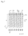
FIG. 7 is a diagram showing how the irradiation regions are corrected to compensate for a displacement of a sample in a rotational direction in the first embodiment.
FIG. 8 is a block diagram of an electron beam exposure apparatus according to a second embodiment.
FIG. 9 is a block diagram of an electron beam exposure apparatus according to a third embodiment.
FIG. 10 is a block diagram of an electron beam exposure apparatus according to a fourth embodiment.
FIG. 11 is a plan view of a beam shaping aperture plate in FIG. 10.
FIG. 12 is a plan view of a blanker plate in FIG. 10.
FIG. 13 is a diagram showing how selecting deflectors in FIG. 10 change a position on the beam shaping aperture irradiated with an electron beam.
FIG. 14 is a block diagram of an electron beam exposure apparatus according to a modification of the fourth embodiment.
FIG. 15 is a block diagram of an electron beam exposure apparatus according to a fifth embodiment.
FIG. 16 is a block diagram of an electron beam exposure apparatus according to a sixth embodiment.
FIG. 17 is a diagram showing an example of how column cells are arranged in the electron beam exposure apparatus in FIG. 16.
DESCRIPTION OF EMBODIMENTS
Before describing embodiments, a description of complementary lithography is given.
FIGS. 1A and 1B are diagrams illustrating complementary lithography.
In complementary lithography, a wiring pattern is formed by alternately superimposing wiring layers each formed by a pattern of lateral lines and wiring layers each formed by a pattern of vertical lines.
FIG. 1A shows an example of a line-and-space pattern on an N-th layer of the wiring layers on a semiconductor substrate and arrangement of cut patterns 83 for cutting line patterns of the line-and-space pattern. In the line-and-space pattern shown in FIG. 1A, line patterns 81 a and spaces 82 a having certain widths and extending laterally (in an X direction) are alternately arranged. This line-and-space pattern is formed using a narrow-pitch technique combining immersion exposure using an ArF light source and double patterning.
The cut patterns 83 are not simple lines but fine rectangular patterns. Thus, it is difficult to form the cut patterns 83 with light exposure using the ArF light source. For this reason, exposure of the cut patterns 83 is performed using electron beams (charged particle beams) excellent in resolution.
In FIG. 1A, lines 84 a, 84 b forming grids are lines set in design data to indicate arrangement positions of patterns. The line patterns 81 a and the spaces 82 a are arranged along the lateral lines 84 a.
The cut patterns 83, on the other hand, are arranged along the vertical lines 84 b. The shape of each cut pattern 83 is not limited as long as it is a rectangular pattern having a length which cuts across the line pattern 81 a vertically. As shown in FIG. 1A, the cut patterns 83 occupy only a small percent of the entire area. Thus, practical throughput can be obtained even with electron beam exposure.
FIG. 1B is a diagram showing an example of a positional relation between a line-and-space pattern on an N+1-th layer and the cut patterns 83 on the N-th layer.
As shown in FIG. 1B, the line-and-space pattern on the N+1-th layer is formed by alternately arranging line patterns 81 b and spaces 82 b having certain widths and extending vertically (in a Y direction). The line patterns 81 b are arranged along the vertical lines 84 b in the design data.
Via holes are formed at intersections of the lateral line patterns 81 a and the vertical line patterns 81 b to connect these patterns to each other.
If displaced laterally, the cut patterns 83 may interfere with the via hole pattern. For this reason, the cut patterns 83 are required to be arranged accurately between the line patterns 81 b, and needs accuracy in the lateral direction. On the other hand, since the vertical length of each cut pattern 83 is larger than the line width of each line pattern 81 a, small vertical displacement of the cut pattern 83 is not so problematic.
Focusing on the properties of the cut patterns 83 described above, an electron beam exposure apparatus with a simple apparatus configuration capable of efficient electron beam exposure using many electron beams is described in the following embodiments.
First Embodiment
FIG. 2 is a block diagram of an electron beam exposure apparatus according to a first embodiment.
As shown in FIG. 2, an electron beam exposure apparatus according to this embodiment includes a cylindrical casing (column cell) 11 housing an electron gun 1 configured to generate an electron beam EB0 and an optical system of the electron beam exposure apparatus 10, a stage device 7 placed below the column cell 11, and a controller 13 configured to control each unit.
The electron gun 1 in the column cell 11 emits the electron beam EB0 having a predetermined accelerating voltage (e.g., 50 keV). By passing through an aperture 2 a of a first aperture plate 2, the electron beam EB0 is shaped into a beam having a circular section symmetrical about an optical axis C.
An asymmetric illumination optical system 3 is placed below the first aperture plate 2, and generates an electron beam EB1 by deforming the electron beam EB0 into a beam having an elongated section which is long in one direction (the X direction) and short in another direction (the Y direction).
FIG. 3 is a perspective view showing an example of the asymmetric illumination optical system 3 as a group of electrostatic quadrupole lenses.
As shown in FIG. 3, the asymmetric illumination optical system 3 is formed of electrostatic quadrupole electrodes 51 a arranged about the optical axis C and stacked in four layers, and generates an electric quadrupole magnetic field near the optical axis C. The electron beam EB1 having an elongated section can be formed through appropriate adjustment of this electrostatic quadrupole magnetic field.
Referring back to FIG. 2, the electron beam EB1 is applied to an irradiation region S1 of a beam shaping aperture plate 21.
The beam shaping aperture plate 21 is provided with a line of aperture portions 21 a arranging in the same direction as a longitudinal direction (X direction) of the irradiation region S1 for the electron beam EB1. These aperture portions 21 a shape the electron beam EB1 into a plurality of electron beams EB3 as many as the aperture portions 21 a.
FIG. 4A is a diagram showing an irradiation region S99 for the electron beam EB1 according to a comparative example, and FIG. 4B is a diagram showing the electron beam irradiation region S1 according to this embodiment.
In the comparative example shown in FIG. 4A, an electron beam which is circular in section is directly applied without using the asymmetric illumination optical system 3. Thus, the aperture portions 21 a occupy a small percentage of the irradiation region S99. In the comparative example, therefore, a majority of electrons emitted from the electron gun 1 are not used and discarded, and the current density of the electron beams EB3 passing through the beam shaping aperture plate 21 is low.
In contrast, in this embodiment, as shown in FIG. 4B, the electron beam EB1 is applied to the beam shaping aperture plate 21 after being elongated by the asymmetric illumination optical system 3. In this case, the aperture portions 21 a occupy an increased percentage of the irradiation region S1 for the electron beam EB1, allowing more electrons to be utilized for the exposure. Hence, the electron beams EB3 with a larger current density can be generated, allowing a pattern to be drawn through radiation of a shorter period of time.
In this embodiment, the aperture portions 21 a of the beam shaping aperture plate 21 are arranged in a line in a direction orthogonal to a direction in which the stage device 7 moves during exposure, so that the plurality of electron beams EB3 move at the same time.
A blanker plate 31 is placed below the beam shaping aperture plate 21 in FIG. 2.
FIG. 5A is an enlarged plan view of the blanker plate 31, and FIG. 5B is a sectional view taken along line in FIG. 5A.
As shown in FIG. 5A, the blanker plate 31 is placed near the beam shaping aperture plate 21, and apertures 31 a are provided in a main body 31 e of the blanker plate 31. The apertures 31 a are each larger than each aperture portion 21 a and permit the electron beams EB3 to pass therethrough. On the sides of each aperture 31 a, blanking electrodes 31 b, 31 c for deflecting the electron beam EB3 are provided. The blanking electrodes 31 b, 31 c are connected to a drive circuit via interconnections 31 d and terminals (not shown). The blanking electrodes 31 b, 31 c and the interconnections 31 d are formed integrally by patterning of a conductive film on the main body 31 e of the blanker plate 31, the conductive film having a thickness of about several micrometers to several tens of micrometers. The blanking electrodes 31 b, 31 c are preferably formed on a surface which corresponds to the downstream side of the electron beams EB3, for prevention of being damaged by radiation of electron beams.
As shown in FIG. 5B, when voltage is applied to the blanking electrodes 31 b, 31 c, the electron beams EB3 having passed through the apertures 31 a are largely bent, as shown with a track denoted as OFF. As a result, as shown in FIG. 2, an electron beam EBOFF bent by the blanking electrodes 31 b, 31 c is led to an outside of an aperture 5 a of a final aperture plate 5 placed below the blanker plate 31, and thus it is blocked to advance toward the stage 7.
When, on the other hand, voltage is not applied to the blanking electrodes 31 b, 31 c, the electron beams EB3 pass through the aperture 5 a of the final aperture plate 5. In other words, ON/OFF control of each of the electron beams EB3 can be achieved by applying or not applying voltage to its corresponding blanking electrodes 31 b, 31 c.
Below the blanker plate 31, a first electromagnetic lens 4 a, a second electromagnetic lens 4 b, a third electromagnetic lens 4 c, and a fourth electromagnetic lens 4 d are provided. Cooperation of these first to fourth electromagnetic lenses 4 a to 4 d enables images of the aperture portions 21 a of the beam shaping aperture plate 21 to be reduced at a predetermined reduction rate α and formed on a surface of a sample 80.
The final aperture plate 5 is placed between the second electromagnetic lens 4 b and the third electromagnetic lens 4 c. The circular aperture 5 a is provided in the final aperture plate 5 near the optical axis C, and only the electron beams EB3 not reflected by the blanker plate 31 pass therethrough the aperture 5 a.
A stage feedback deflector 6 is provided below the final aperture plate 5. This stage feedback deflector 6 has a pair of electrode plates arranged along the line of the aperture portions 21 a (the X direction) in such a manner as to sandwich the optical axis C. The stage feedback deflector 6 allows fine adjustment of the irradiation position of the electron beams EB3 in the X direction.
The stage device 7 is provided below the column cell 11. The stage device 7 retains the sample 80 on its upper surface, and is enabled by a drive device 8 to move horizontally and rotate.
Alongside the stage device 7, a position sensor 9 formed of a laser interferometer, a line sensor, or the like is provided to allow accurate measurement of the position of the stage device 7 with a resolution in the order of a micrometer. A detection result of the position sensor 9 is used for control of the drive device 8 and control of the stage feedback deflector 6.
In the electron beam exposure apparatus 10 according to this embodiment described above, exposure of cut patterns and via holes is performed while moving the stage device 7 in the direction orthogonal to the line of the aperture portions 21 a (the X direction). The following describes an exposure method for drawing a pattern in this embodiment.
FIG. 6A is a diagram showing irradiation regions 23 of electron beams for exposure of the line patterns 81 a on the N-th layer, and FIG. 6B is an enlarged diagram showing the shapes and an arrangement of the aperture portions 21 a of the beam shaping aperture plate 21. Note that, in FIG. 6B, the aperture portions 21 a for exposure of a cut pattern is illustrated as an example. Although cut patterns are described herein, a similar exposure method can be used for via-hole patterns as well by changing the shapes and irradiation positions.
As shown in FIG. 6A, the electron beams EB3 are applied to a surface of the sample 80 at the irradiation regions 23 which are obtained by reducing the image of aperture portions 21 a at the predetermined reduction rate α. These irradiation regions 23 are rectangular and positioned at the space portions between the line patterns 81 b on the N+1-th layer.
A pitch P2 of the irradiation regions 23 is the same as the pitch of the line patterns 81 b on the N+1-th layer. An X-direction width A2 of each irradiation region 23 is set to be equal to or smaller than a width D2 of a space between the adjacent line patterns 81 b. A Y-direction length B2 of the irradiation region 23 is set to be larger than a width D1 of the line pattern 81 a on the N-th layer.
To form such irradiation region 23, a width A1, a length B1, and a pitch P1 of each aperture portion 21 a of the beam shaping aperture plate 21 are reduced by the predetermined reduction rate α to achieve the width A2, the length B2, and the pitch P2 of the irradiation region 23.
Note that the width, length, and pitch of cut patterns vary according to a process node defining the line width and pitch of line patterns. Thus, in this embodiment, exposure of the sample 80 for a different process node can be performed using a different beam shaping aperture plate 21 provided with the aperture portions 21 a of size and pitch corresponding to that process node.
Next, while moving the stage device 7 in the direction denoted by arrow M in FIG. 6A under the control of the controller 13, exposure of cut patterns is performed by turning desired electron beams EB3 on at the timing when the irradiation regions 23 overlap the line patterns 81 a on the N-th layer in a crossing manner.
In this embodiment, the positional shift of the stage device 7 in the X direction is constantly detected by the position sensor 9, and based on the detection result, the stage feedback deflector 6 causes the X-direction positions of the irradiation regions 23 to follow the surface of the sample 80 to ensure accuracy in the X direction.
The stage feedback deflector 6 is also used for correction of error due to a displacement of the sample 80 in the rotational direction.
FIG. 7 is a plan view illustrating a method of correcting the irradiation regions 23 to compensate for displacement of the sample 80 in the rotational direction.
The displacement in the rotational direction occurs due to the mechanical accuracy of the stage device 7 or an error caused in placing the sample 80 on the stage device 7. As shown in FIG. 7, as the stage device 7 moves more in the Y direction, a positional shift ΔX in the X direction increases. Thus, an angular shift Δθ of the sample 80 in the rotational direction is measured in advance using a positioning mark or the like. And, by the stage feedback deflector 6, the positional shift in the X direction of the irradiation regions 23 occurring with the movement of the stage device 7 in the Y direction is compensated for. Thereby, even if the sample 80 is displaced in the rotational direction, exposure of cut patterns can be performed with high accuracy.
As described above, according to the electron beam exposure apparatus 10 of this embodiment, the aperture portions 21 a of the beam shaping aperture plate 21 are arranged in a line one-dimensionally, and the asymmetric illumination optical system 3 changes electron beams in shape so that they may have a flat section corresponding to the line of the aperture portions 21 a. Thereby, exposure using a plurality of electron beams EB3 can be performed with high current density without increasing the amount of electrons emitted from the electron gun 1. Thus, exposure of many via-holes and cut patterns can be performed with a short period of time.
In addition, the positioning of the electron beams EB3 can be achieved only with the stage feedback deflector 6, and therefore the electron optical system can be simplified.
Second Embodiment
FIG. 8 is a block diagram of an electron beam exposure apparatus 20 according to a second embodiment. Note that configurations of the electron beam exposure apparatus 20 of this embodiment which are the same as those of the electron beam exposure apparatus 10 in FIG. 2 are denoted by the same reference numerals as those used in FIG. 2, and are not described in detail.
As shown in FIG. 8, the electron beam exposure apparatus 20 of this embodiment is different from the electron beam exposure apparatus 10 in that a primary beam shaping plate 41 is placed between the asymmetric illumination optical system 3 and the beam shaping aperture plate 21.
The primary beam shaping plate 41 has a rectangular slit 41 a which is slightly larger in width and length than the line of the aperture portions 21 a of the beam shaping aperture plate 21. This slit 41 a shapes the electron beam EB1 into a beam having a rectangular section and forms a rectangular irradiation region S2 on the beam shaping aperture plate 21.
In this embodiment, the provision of the primary beam shaping plate 41 enables reduction of the amount of electrons with which to irradiate the beam shaping aperture plate 21. This allows prevention of deterioration or damage of the beam shaping aperture plate 21 due to heating up.
The beam shaping aperture plate 21 is an expensive component because highly-accurate microfabrication is performed thereon to form the aperture portions 21 a. Thus, deterioration or damage of the beam shaping aperture plate 21 leads to an increase in running costs. Moreover, when the beam shaping aperture plate 21 is deteriorated and requires replacement, the apparatus needs to be stopped, which consequently lowers utilization of the apparatus.
In contrast, in this embodiment, deterioration or damage of the beam shaping aperture plate 21 due to electron beams can be reduced, achieving improvement in the utilization and reduction in operational costs of the electron beam exposure apparatus 20.
In this embodiment, one or a plurality of pairs of electromagnetic lenses for formation of an image of the slit 41 a may be provided between the primary beam shaping plate 41 and the beam shaping aperture plate 21. In such a case, the irradiation region S2 on the beam shaping aperture plate 21 can be formed into a sharper shape, allowing reduction in the aberration of electron beams. As a result, sharper images of the aperture portions 21 a can be formed on the surface of the sample 80, allowing exposure of fine patterns with high accuracy.
Third Embodiment
FIG. 9 is a block diagram of an electron beam exposure apparatus 30 according to a third embodiment. Note that configurations of the electron beam exposure apparatus 30 which are the same as those of the electron beam exposure apparatuses 10 and 20 illustrated in FIGS. 2 to 8 are denoted by the same reference numerals as those used in FIGS. 2 to 8, and are not described in detail.
As shown in FIG. 9, the electron beam exposure apparatus 30 of this embodiment has a primary beam shaping plate 42 and electromagnetic lenses 61 a, 61 b between the asymmetric illumination optical system 3 and the beam shaping aperture plate 21.
The primary beam shaping plate 42 is provided with a line of rectangular aperture portions 42 a arranged in the X direction as many as the aperture portions 21 a. The aperture portions 42 a are larger than the aperture portions 21 a of the beam shaping aperture plate 21, and are formed at almost the same pitch as the aperture portions 21 a.
The electron beam EB1 shaped to be flat by the asymmetric illumination optical system 3 is applied to an irradiation region S1 of the primary beam shaping plate 42. Then, by passing through the aperture portions 42 a of the primary beam shaping plate 42, the electron beam EB1 is shaped into a plurality of rectangular electron beams EB11.
Images of the electron beams EB11 are formed on the beam shaping aperture plate 21 by the electromagnetic lens 61 a and the electromagnetic lens 61 b, and the electron beams EB11 are thus applied to irradiation regions S11 which correspond to the respective aperture portions 21 a of the beam shaping aperture plate 21.
According to this embodiment, the primary beam shaping plate 42 can reduce the amount of electrons with which to irradiate the beam shaping aperture plate 21, compared to a case of using the slit 41 a of the primary beam shaping plate 41. Thus, deterioration or damage of the beam shaping aperture plate 21 can be prevented more effectively.
Moreover, the current amount of the electron beams EB11 is reduced by the primary beam shaping plate 42; therefore, chromatic aberration due to coulomb interaction of electrons (variation in speed of the electrons) can be reduced, allowing improvement in the fineness of exposure patterns.
Fourth Embodiment
FIG. 10 is a block diagram of an electron beam exposure apparatus 40 according to a fourth embodiment. Note that configurations of the electron beam exposure apparatus 40 which are the same as those of the electron beam exposure apparatuses 10, 20, and 30 described with reference to FIGS. 2 to 9 are denoted by the same reference numerals as those used in FIGS. 2 to 9, and are not described in detail.
As shown in FIG. 10, the electron beam exposure apparatus 40 of this embodiment has a beam shaping aperture plate 22 provided with a plurality of lines of aperture portions 21 a, a blanker plate 34 corresponding to the beam shaping aperture plate 22, first and second selecting deflectors 62 a and 62 b for selecting between the lines of the aperture portions 21 a.
FIG. 11 is a partially enlarged view of the beam shaping aperture plate 22 according to this embodiment.
As shown in FIG. 11, the beam shaping aperture plate 22 of this embodiment is provided with at least two lines of aperture portions 21 a arranged in the X direction, the lines being apart from each other in the Y direction. The aperture portions 21 a of one line and the aperture portions 21 a of the other line have the same shape and located at positions coinciding in the X direction. Although there are two lines of the aperture portions 21 a in the example shown in FIG. 11, this embodiment is not limited to this, and may have three or more lines.
As shown in FIG. 10, the blanker plate 34 is placed below the beam shaping aperture plate 22.
FIG. 12 is a plan view of the blanker plate 34. This blanker plate 34 is provided with aperture portions 31 a at portions corresponding to the aperture portions 21 a of the beam shaping aperture plate 22. Each aperture portion 31 a is larger than each aperture portion 21 a, and allows an electron beam having passed through the aperture portion 21 a to pass therethrough.
The blanking electrodes 31 b, 31 c are provided on the respective sides of each aperture portion 31 a. In this embodiment, the blanking electrodes 31 b for the aperture portions 31 a formed at positions coinciding in the X direction are connected to each other in parallel via an interconnection 37 a, and the blanking electrodes 31 c for the aperture portions 31 a formed at positions coinciding in the X direction are connected to each other in parallel via an interconnection 37 b.
This eliminates the need for increasing the number of drive circuits 65 a, 65 b even if the aperture portions 31 a arranged in parallel are increased in number. This can simplify the configuration of the apparatus.
Further, as shown in FIG. 10, the first selecting deflector 62 a and the second selecting deflector 62 b are provided above the beam shaping aperture plate 22.
The first selecting deflector 62 a deflects the electron beam EB1 having passed through the primary beam shaping plate 41 in the Y direction, and the second selecting deflector 62 b aligns the electron beam EB1 having been deflected by the first selecting deflector 62 a so that the electron beam EB1 may be in parallel with the optical axis C.
FIG. 13 is a diagram showing how the selecting deflectors 62 a, 62 b change the irradiation region S2 for the electron beam EB1.
As the arrow in FIG. 13 shows, the first selecting deflector 62 a and the second selecting deflector 62 b can switch the irradiation region S2 to a different line of the aperture portions 21 a on the beam shaping aperture plate 22.
When exposure is performed for a long period of time using the electron beam exposure apparatus 40, any of the electron beams EB3 might experience abnormality due to abnormal blanking operation of the aperture portions 31 a of the blanker plate 34 or deterioration of the beam shaping aperture plate 21.
Even in such a case, as shown in FIG. 13, the exposure can be continued without stopping the electron beam exposure apparatus 40 by switching to a different line of the aperture portions 21 a by use of the selecting deflectors 62 a, 62 b.
Another Example of the Fourth Embodiment
FIG. 14 is a partially enlarged view of a beam shaping aperture plate 23 according to a modification of the fourth embodiment.
As shown in FIG. 14, the beam shaping aperture plate 23 of this modification is provided with a plurality of lines of aperture portions, namely, a line of aperture portions 21 a to a line of aperture portions 21 d, the aperture portions being different in shape, size, and pitch from one line to another.
Specifically, the beam shaping aperture plate 23 is provided with a line of the aperture portions 21 a for cut patterns and a line of the aperture portions 21 b for via-hole patterns, and for a different process node, a line of aperture portions 21 c for cut patterns and a line of aperture portions 21 d for via-hole patterns.
In this modification, switch can be made between exposure of cut patterns and exposure of via-hole patterns by changing the irradiation position of the electron beam EB1 from the line of the aperture portions 21 a to the line to the aperture portions 21 b by use of the selecting deflectors 62 a, 62 b.
Further, to perform exposure for the sample 80 on which wiring patterns for different process nodes coexist, the exposure can be continued by changing the irradiation position of the electron beam EB1 from, for example, the line of the aperture portions 21 a to the line of the aperture portions 21 c.
Thereby, the beam shaping aperture plate does not need to be changed. Thus, exposure of cut patterns or via-hole patterns can be performed without stopping the electron beam exposure apparatus 40.
Fifth Embodiment
FIG. 15 is a block diagram of an electron beam exposure apparatus 50 according to a fifth embodiment. Note that configurations of the electron beam exposure apparatus 50 which are the same as those of the electron beam exposure apparatuses 10, 20, 30, and 40 shown in FIGS. 2 to 14 are denoted by the same reference numerals as those used in FIGS. 2 to 14, and are not described in detail.
As shown in FIG. 15, the electron beam exposure apparatus 50 includes electromagnetic deflectors 63 a, 63 b between the asymmetric illumination optical system 3 and the primary beam shaping plate 42. The electromagnetic deflectors 63 a, 63 b are configured to adjust the irradiation position of the electron beam EB1 on a primary beam shaping plate 43.
The primary beam shaping plate 43 is provided with a plurality of apertures 43 a, 43 b, 43 c. The aperture 43 a is a slit elongated in the X direction, and the apertures 43 b are rectangular apertures arranged in a line in the X direction. The aperture 43 c is a slit elongated in the Y direction.
In the electron beam exposure apparatus 50 of this embodiment, the electromagnetic deflectors 63 a, 63 b are used to irradiate one of the apertures 43 a to 43 c with the elongated electron beam EB1.
An aperture elongated in the Y direction, like the aperture 43 c, can be irradiated with the electron beam EB1 by shifting, by 90° around the optical axis, a combination of voltages to be applied to the electrodes 51 a of the asymmetric illumination optical system 3 (electrostatic quadrupole deflector) shown in FIG. 3.
A beam shaping aperture plate 24 is provided below the primary beam shaping plate 43. The beam shaping aperture plate 24 of this embodiment is provided with a plurality of aperture portions 21 a, 24 a at positions corresponding to the apertures 43 a, 43 b, 43 c of the primary beam shaping plate 43. Among the aperture portions 21 a, 24 a, the aperture portions 24 a are arranged in a line in the Y direction.
Electron beams having passed through the aperture portions 24 a form a line in the Y direction. Thus, exposure of cut patterns for patterns extending in the Y direction can be performed by applying the electron beams while moving the stage device 7 in the X direction.
Hence, the electron beam exposure apparatus 50 of this embodiment enables exposure of cut patterns for the line patterns 81 a extending in the X direction and cut patterns for the line patterns 81 b extending in the Y direction without rotating the sample 80 by 90°.
Sixth Embodiment
FIG. 16 is a block diagram of an electron beam exposure apparatus 60 according to a sixth embodiment. Note that configurations of the electron beam exposure apparatus 60 of this embodiment which are the same as those of the electron beam exposure apparatuses 10, 20, 30, 40, and 50 shown in FIGS. 2 to 15 are denoted by the same reference numerals as those used in FIGS. 2 to 15, and are not described in detail.
As shown in FIG. 16, the electron beam exposure apparatus 60 of this embodiment includes a plurality of column cells 11 inside a vacuum chamber 12, and the stage device 7 configured to retain the sample 80 is provided below these column cells 11. Each of the column cells 11 houses components constituting an electron optical system, such an electron gun, a beam shaping aperture plate, a blanker plate, a final aperture plate, a group of electromagnetic lenses, and a stage feedback deflector (see FIGS. 2 to 15). Each column cell 11 emits about, for example, two thousand electron beams EB3.
FIG. 17 is a plan view showing an example of an arrangement of the column cells 11 of the electron beam exposure apparatus 60 in FIG. 16.
As shown in FIG. 17, the column cells 11 are each formed in a cylindrical shape having a diameter of about, for example, 40 mm. For example, sixty column cells 11 are arranged above a semiconductor wafer (the sample 80) having a diameter of 300 mm to 400 mm. The plurality of electron beams EB3 generated by the column cells 11 are applied to irradiation regions 66 having a width shown in FIG. 17.
Exposure of cut patterns or via-hole patterns is performed with respect to a surface of the sample 80 while moving the sample 80 in a Y1 or Y2 direction as shown with the arrows in FIG. 17. After moving the sample 80 about 40 mm, which is as long as the pitch of the column cells 11, in the Y1 or Y2 direction, the sample 80 is moved a distance corresponding to the width of the irradiation region 66 in an X1 direction, and then moved in the Y1 or Y2 direction. Exposure is thus performed.
According to this embodiment, exposure is performed using the plurality of column cells 11 to use many electron beams at the same time; therefore, throughput of exposure improves more.
In a case where sixty column cells 11 each configured to generate two thousand electron beams EB3 are provided, exposure can be performed with 120,000 electron beams EB3 in total.
The speed of exposure was estimated provided that the exposure is performed with respect to a resist having a sensitivity of 100 μC/cm2 with the column cells 11 being arranged in number which makes an area exposed by each column cell 11 about 900 mm2. As a result, it was confirmed that about ten wafers can be processed per hour.