US9477122B2 - Display device - Google Patents
Display device Download PDFInfo
- Publication number
- US9477122B2 US9477122B2 US14/456,119 US201414456119A US9477122B2 US 9477122 B2 US9477122 B2 US 9477122B2 US 201414456119 A US201414456119 A US 201414456119A US 9477122 B2 US9477122 B2 US 9477122B2
- Authority
- US
- United States
- Prior art keywords
- electrode
- display device
- insulating layer
- voltage application
- application unit
- Prior art date
- Legal status (The legal status is an assumption and is not a legal conclusion. Google has not performed a legal analysis and makes no representation as to the accuracy of the status listed.)
- Active, expires
Links
- 230000002093 peripheral effect Effects 0.000 claims abstract description 33
- 239000004020 conductor Substances 0.000 claims description 22
- 239000000758 substrate Substances 0.000 claims description 12
- 239000000463 material Substances 0.000 claims description 7
- 239000007769 metal material Substances 0.000 claims description 4
- 239000011368 organic material Substances 0.000 claims description 2
- 239000010410 layer Substances 0.000 description 119
- 238000002161 passivation Methods 0.000 description 41
- 239000004065 semiconductor Substances 0.000 description 19
- 239000010409 thin film Substances 0.000 description 16
- 239000011810 insulating material Substances 0.000 description 13
- 229910052751 metal Inorganic materials 0.000 description 10
- 239000002184 metal Substances 0.000 description 10
- 239000004973 liquid crystal related substance Substances 0.000 description 9
- ZOKXTWBITQBERF-UHFFFAOYSA-N Molybdenum Chemical compound [Mo] ZOKXTWBITQBERF-UHFFFAOYSA-N 0.000 description 8
- 229910052750 molybdenum Inorganic materials 0.000 description 8
- 239000011733 molybdenum Substances 0.000 description 8
- 230000000903 blocking effect Effects 0.000 description 7
- 239000010949 copper Substances 0.000 description 7
- 238000004519 manufacturing process Methods 0.000 description 7
- 229910045601 alloy Inorganic materials 0.000 description 6
- 239000000956 alloy Substances 0.000 description 6
- 229910052782 aluminium Inorganic materials 0.000 description 6
- XAGFODPZIPBFFR-UHFFFAOYSA-N aluminium Chemical compound [Al] XAGFODPZIPBFFR-UHFFFAOYSA-N 0.000 description 6
- 239000011651 chromium Substances 0.000 description 6
- 239000003086 colorant Substances 0.000 description 6
- 238000010586 diagram Methods 0.000 description 6
- RYGMFSIKBFXOCR-UHFFFAOYSA-N Copper Chemical compound [Cu] RYGMFSIKBFXOCR-UHFFFAOYSA-N 0.000 description 5
- 229910052802 copper Inorganic materials 0.000 description 5
- 238000000034 method Methods 0.000 description 5
- 239000010936 titanium Substances 0.000 description 5
- VYZAMTAEIAYCRO-UHFFFAOYSA-N Chromium Chemical compound [Cr] VYZAMTAEIAYCRO-UHFFFAOYSA-N 0.000 description 4
- BQCADISMDOOEFD-UHFFFAOYSA-N Silver Chemical compound [Ag] BQCADISMDOOEFD-UHFFFAOYSA-N 0.000 description 4
- 229910052804 chromium Inorganic materials 0.000 description 4
- 229910052709 silver Inorganic materials 0.000 description 4
- 239000004332 silver Substances 0.000 description 4
- RTAQQCXQSZGOHL-UHFFFAOYSA-N Titanium Chemical compound [Ti] RTAQQCXQSZGOHL-UHFFFAOYSA-N 0.000 description 3
- 229910021417 amorphous silicon Inorganic materials 0.000 description 3
- 238000005259 measurement Methods 0.000 description 3
- 230000003071 parasitic effect Effects 0.000 description 3
- 229910052715 tantalum Inorganic materials 0.000 description 3
- GUVRBAGPIYLISA-UHFFFAOYSA-N tantalum atom Chemical compound [Ta] GUVRBAGPIYLISA-UHFFFAOYSA-N 0.000 description 3
- 229910052719 titanium Inorganic materials 0.000 description 3
- 229910001316 Ag alloy Inorganic materials 0.000 description 2
- 229910000838 Al alloy Inorganic materials 0.000 description 2
- 229910000881 Cu alloy Inorganic materials 0.000 description 2
- 229910001182 Mo alloy Inorganic materials 0.000 description 2
- VYPSYNLAJGMNEJ-UHFFFAOYSA-N Silicium dioxide Chemical compound O=[Si]=O VYPSYNLAJGMNEJ-UHFFFAOYSA-N 0.000 description 2
- 230000005684 electric field Effects 0.000 description 2
- 239000010408 film Substances 0.000 description 2
- 239000011521 glass Substances 0.000 description 2
- 239000012535 impurity Substances 0.000 description 2
- 239000011159 matrix material Substances 0.000 description 2
- 230000000704 physical effect Effects 0.000 description 2
- 229910021420 polycrystalline silicon Inorganic materials 0.000 description 2
- 229920005591 polysilicon Polymers 0.000 description 2
- 239000003870 refractory metal Substances 0.000 description 2
- 229910052814 silicon oxide Inorganic materials 0.000 description 2
- 238000002834 transmittance Methods 0.000 description 2
- 201000005569 Gout Diseases 0.000 description 1
- OAICVXFJPJFONN-UHFFFAOYSA-N Phosphorus Chemical compound [P] OAICVXFJPJFONN-UHFFFAOYSA-N 0.000 description 1
- 229910052581 Si3N4 Inorganic materials 0.000 description 1
- 229910004205 SiNX Inorganic materials 0.000 description 1
- 230000005540 biological transmission Effects 0.000 description 1
- 239000003990 capacitor Substances 0.000 description 1
- AMGQUBHHOARCQH-UHFFFAOYSA-N indium;oxotin Chemical compound [In].[Sn]=O AMGQUBHHOARCQH-UHFFFAOYSA-N 0.000 description 1
- 238000009413 insulation Methods 0.000 description 1
- 238000012986 modification Methods 0.000 description 1
- 230000004048 modification Effects 0.000 description 1
- 239000012044 organic layer Substances 0.000 description 1
- 229910052698 phosphorus Inorganic materials 0.000 description 1
- 239000011574 phosphorus Substances 0.000 description 1
- 239000000049 pigment Substances 0.000 description 1
- 230000010287 polarization Effects 0.000 description 1
- 229910021332 silicide Inorganic materials 0.000 description 1
- FVBUAEGBCNSCDD-UHFFFAOYSA-N silicide(4-) Chemical compound [Si-4] FVBUAEGBCNSCDD-UHFFFAOYSA-N 0.000 description 1
- HQVNEWCFYHHQES-UHFFFAOYSA-N silicon nitride Chemical compound N12[Si]34N5[Si]62N3[Si]51N64 HQVNEWCFYHHQES-UHFFFAOYSA-N 0.000 description 1
- YVTHLONGBIQYBO-UHFFFAOYSA-N zinc indium(3+) oxygen(2-) Chemical compound [O--].[Zn++].[In+3] YVTHLONGBIQYBO-UHFFFAOYSA-N 0.000 description 1
Images


Classifications
-
- F—MECHANICAL ENGINEERING; LIGHTING; HEATING; WEAPONS; BLASTING
- F24—HEATING; RANGES; VENTILATING
- F24D—DOMESTIC- OR SPACE-HEATING SYSTEMS, e.g. CENTRAL HEATING SYSTEMS; DOMESTIC HOT-WATER SUPPLY SYSTEMS; ELEMENTS OR COMPONENTS THEREFOR
- F24D17/00—Domestic hot-water supply systems
- F24D17/0005—Domestic hot-water supply systems using recuperation of waste heat
-
- G—PHYSICS
- G02—OPTICS
- G02F—OPTICAL DEVICES OR ARRANGEMENTS FOR THE CONTROL OF LIGHT BY MODIFICATION OF THE OPTICAL PROPERTIES OF THE MEDIA OF THE ELEMENTS INVOLVED THEREIN; NON-LINEAR OPTICS; FREQUENCY-CHANGING OF LIGHT; OPTICAL LOGIC ELEMENTS; OPTICAL ANALOGUE/DIGITAL CONVERTERS
- G02F1/00—Devices or arrangements for the control of the intensity, colour, phase, polarisation or direction of light arriving from an independent light source, e.g. switching, gating or modulating; Non-linear optics
- G02F1/01—Devices or arrangements for the control of the intensity, colour, phase, polarisation or direction of light arriving from an independent light source, e.g. switching, gating or modulating; Non-linear optics for the control of the intensity, phase, polarisation or colour
- G02F1/13—Devices or arrangements for the control of the intensity, colour, phase, polarisation or direction of light arriving from an independent light source, e.g. switching, gating or modulating; Non-linear optics for the control of the intensity, phase, polarisation or colour based on liquid crystals, e.g. single liquid crystal display cells
- G02F1/133—Constructional arrangements; Operation of liquid crystal cells; Circuit arrangements
- G02F1/1333—Constructional arrangements; Manufacturing methods
- G02F1/1345—Conductors connecting electrodes to cell terminals
- G02F1/13454—Drivers integrated on the active matrix substrate
-
- G—PHYSICS
- G09—EDUCATION; CRYPTOGRAPHY; DISPLAY; ADVERTISING; SEALS
- G09G—ARRANGEMENTS OR CIRCUITS FOR CONTROL OF INDICATING DEVICES USING STATIC MEANS TO PRESENT VARIABLE INFORMATION
- G09G3/00—Control arrangements or circuits, of interest only in connection with visual indicators other than cathode-ray tubes
- G09G3/20—Control arrangements or circuits, of interest only in connection with visual indicators other than cathode-ray tubes for presentation of an assembly of a number of characters, e.g. a page, by composing the assembly by combination of individual elements arranged in a matrix no fixed position being assigned to or needed to be assigned to the individual characters or partial characters
- G09G3/34—Control arrangements or circuits, of interest only in connection with visual indicators other than cathode-ray tubes for presentation of an assembly of a number of characters, e.g. a page, by composing the assembly by combination of individual elements arranged in a matrix no fixed position being assigned to or needed to be assigned to the individual characters or partial characters by control of light from an independent source
- G09G3/36—Control arrangements or circuits, of interest only in connection with visual indicators other than cathode-ray tubes for presentation of an assembly of a number of characters, e.g. a page, by composing the assembly by combination of individual elements arranged in a matrix no fixed position being assigned to or needed to be assigned to the individual characters or partial characters by control of light from an independent source using liquid crystals
-
- E—FIXED CONSTRUCTIONS
- E03—WATER SUPPLY; SEWERAGE
- E03C—DOMESTIC PLUMBING INSTALLATIONS FOR FRESH WATER OR WASTE WATER; SINKS
- E03C1/00—Domestic plumbing installations for fresh water or waste water; Sinks
- E03C2001/005—Installations allowing recovery of heat from waste water for warming up fresh water
-
- G—PHYSICS
- G09—EDUCATION; CRYPTOGRAPHY; DISPLAY; ADVERTISING; SEALS
- G09G—ARRANGEMENTS OR CIRCUITS FOR CONTROL OF INDICATING DEVICES USING STATIC MEANS TO PRESENT VARIABLE INFORMATION
- G09G2300/00—Aspects of the constitution of display devices
- G09G2300/04—Structural and physical details of display devices
- G09G2300/0404—Matrix technologies
- G09G2300/0408—Integration of the drivers onto the display substrate
-
- G—PHYSICS
- G09—EDUCATION; CRYPTOGRAPHY; DISPLAY; ADVERTISING; SEALS
- G09G—ARRANGEMENTS OR CIRCUITS FOR CONTROL OF INDICATING DEVICES USING STATIC MEANS TO PRESENT VARIABLE INFORMATION
- G09G3/00—Control arrangements or circuits, of interest only in connection with visual indicators other than cathode-ray tubes
- G09G3/20—Control arrangements or circuits, of interest only in connection with visual indicators other than cathode-ray tubes for presentation of an assembly of a number of characters, e.g. a page, by composing the assembly by combination of individual elements arranged in a matrix no fixed position being assigned to or needed to be assigned to the individual characters or partial characters
- G09G3/34—Control arrangements or circuits, of interest only in connection with visual indicators other than cathode-ray tubes for presentation of an assembly of a number of characters, e.g. a page, by composing the assembly by combination of individual elements arranged in a matrix no fixed position being assigned to or needed to be assigned to the individual characters or partial characters by control of light from an independent source
- G09G3/36—Control arrangements or circuits, of interest only in connection with visual indicators other than cathode-ray tubes for presentation of an assembly of a number of characters, e.g. a page, by composing the assembly by combination of individual elements arranged in a matrix no fixed position being assigned to or needed to be assigned to the individual characters or partial characters by control of light from an independent source using liquid crystals
- G09G3/3611—Control of matrices with row and column drivers
- G09G3/3648—Control of matrices with row and column drivers using an active matrix
-
- Y—GENERAL TAGGING OF NEW TECHNOLOGICAL DEVELOPMENTS; GENERAL TAGGING OF CROSS-SECTIONAL TECHNOLOGIES SPANNING OVER SEVERAL SECTIONS OF THE IPC; TECHNICAL SUBJECTS COVERED BY FORMER USPC CROSS-REFERENCE ART COLLECTIONS [XRACs] AND DIGESTS
- Y02—TECHNOLOGIES OR APPLICATIONS FOR MITIGATION OR ADAPTATION AGAINST CLIMATE CHANGE
- Y02T—CLIMATE CHANGE MITIGATION TECHNOLOGIES RELATED TO TRANSPORTATION
- Y02T10/00—Road transport of goods or passengers
- Y02T10/10—Internal combustion engine [ICE] based vehicles
- Y02T10/12—Improving ICE efficiencies
Definitions
- the invention relates to a display device.
- a display device includes a plurality of pixels which are an image-displaying unit of the display device and defined in a display panel of the display device, and drivers configured to drive the pixels.
- the drivers include a data driver applying a data voltage to the pixels, and a gate driver applying a gate signal to the pixels for controlling transfer of the data voltage.
- the gate driver and/or the data driver are mounted on a printed circuit board (“PCB”) in a chip type structure to be connected to the display panel or the driver chip is mounted directly on the display panel.
- PCB printed circuit board
- the gate driver includes a shift register including a plurality of stages which are connected dependently, and a plurality of signal lines transferring the driving signal thereto.
- the plurality of stages includes a plurality of thin film transistors and capacitors. Each of the plurality of stages is connected to one gate line among a plurality of gate lines of the display panel, and the plurality of stages sequentially output the gate signal to each of the gate lines according to a predetermined order.
- a display panel includes a display area in which an image is displayed and a non-display area in which an image is not displayed.
- a gate driver of the display device is integrated in the display panel (e.g., not a chip type structure)
- the region occupied by the gate driver is mostly a non-display region of the display panel in which an image is not displayed. Accordingly, as the region occupied by the gate driver is increased, the non-display area of the display panel, particularly, the peripheral area surrounding the display area displaying the image, is increased.
- a bezel of the display device representing the planar area of the peripheral area is increased, thereby reducing an overall display area of the display device and reducing a consumer's satisfaction for the display device. Therefore, reducing a size of the bezel of the display device is desired.
- One or more exemplary embodiment of the invention provides a display device with a reduced area occupied by the gate driver.
- An exemplary embodiment of a display device includes: a display panel including a display area in which a pixel is disposed and a peripheral area adjacent to the display area; and a gate driver in the peripheral area.
- the gate driver includes a transistor unit, and a common voltage application unit which provides a common voltage.
- the common voltage application unit overlaps the transistor unit via a first insulating layer therebetween.
- a common electrode in the display area may be further included, and the common electrode and the common voltage application unit may be connected to each other.
- the common electrode and the common voltage application unit may be directly connected to each other.
- the common electrode and the common voltage application unit may include different materials.
- An edge of the common voltage application unit may overlap the common electrode.
- a contact assistant on the first insulating layer may be further included, and an opening may be defined in the common voltage application unit and expose the contact assistant.
- the pixel may include a switching element, a pixel electrode connected to the switching element, and a common electrode which transmits the common voltage, the pixel electrode and the common electrode may be on the first insulating layer, and the pixel electrode and the common electrode may overlap each other via a second insulating layer therebetween.
- the transistor unit may include two transistors, each transistor may include a gate electrode, a source electrode and a drain electrode, and the drain electrode may be connected to a contact assistant disposed on the second insulating layer.
- a first contact hole may be defined in the first insulating layer and expose the drain electrode, and the drain electrode may be connected to the contact assistant through the first contact hole.
- a gate line which transmits a gate signal to the pixel may be further included, a second contact hole may be defined in the first insulating layer and expose an end of the gate line, and the contact assistant may be connected to the end of the gate line through the second contact hole.
- the common electrode may include a metal material, and the common voltage application unit may include a transparent conductive material.
- the first insulating layer may include an organic material.
- a line width of the common electrode application unit may be expanded.
- the parasitic capacitance therebetween may be reduced.
- FIG. 1 is a block diagram of an exemplary embodiment of a display device according to the invention.
- FIG. 2 is a schematic circuit diagram of an exemplary embodiment of one pixel of a display device according to the invention.
- FIG. 3 is a schematic block diagram of an exemplary embodiment of a display device according to the invention.
- FIG. 4 is an enlarged top plan view of portion “A” of FIG. 3 .
- FIG. 5 is a top plan view of an exemplary embodiment of a common voltage application unit and a common electrode in the display device shown in FIG. 4 .
- FIG. 6 is a cross-sectional view taken along line VI-VI of FIG. 5 .
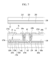
- FIG. 7 is a cross-sectional view taken along line VII-VII of FIG. 5 .
- FIG. 8 is a top plan view of an exemplary embodiment of a liquid crystal display according to the invention.
- FIG. 9 is a cross-sectional view taken along line IX-IX of FIG. 8 .
- first, second, third, etc. may be used herein to describe various elements, components, regions, layers and/or sections, these elements, components, regions, layers and/or sections should not be limited by these terms. These terms are only used to distinguish one element, component, region, layer or section from another element, component, region, layer or section. Thus, a first element, component, region, layer or section discussed below could be termed a second element, component, region, layer or section without departing from the teachings of the invention.
- spatially relative terms such as “lower,” “under,” “above,” “upper” and the like, may be used herein for ease of description to describe the relationship of one element or feature to another element(s) or feature(s) as illustrated in the figures. It will be understood that the spatially relative terms are intended to encompass different orientations of the device in use or operation, in addition to the orientation depicted in the figures. For example, if the device in the figures is turned over, elements described as “under” relative to other elements or features would then be oriented “above” relative to the other elements or features. Thus, the exemplary term “under” can encompass both an orientation of above and below. The device may be otherwise oriented (rotated 90 degrees or at other orientations) and the spatially relative descriptors used herein interpreted accordingly.
- Embodiments of the invention are described herein with reference to cross-section illustrations that are schematic illustrations of idealized embodiments (and intermediate structures) of the invention. As such, variations from the shapes of the illustrations as a result, for example, of manufacturing techniques and/or tolerances, are to be expected. Thus, embodiments of the invention should not be construed as limited to the particular shapes of regions illustrated herein but are to include deviations in shapes that result, for example, from manufacturing.
- “About” or “approximately” as used herein is inclusive of the stated value and means within an acceptable range of deviation for the particular value as determined by one of ordinary skill in the art, considering the measurement in question and the error associated with measurement of the particular quantity (i.e., the limitations of the measurement system). For example, “about” can mean within one or more standard deviations, or within ⁇ 30%, 20%, 10%, 5% of the stated value.
- FIG. 1 and FIG. 2 An exemplary embodiment of a display device according to the invention will be described with reference to FIG. 1 and FIG. 2 .
- FIG. 1 is a block diagram of an exemplary embodiment of a display device according to the invention
- FIG. 2 is a schematic circuit diagram of an exemplary embodiment of one pixel of a display device according to the invention.
- a display device includes a display panel 300 , a gate driver 400 , a data driver 500 and a signal controller 600 .
- the display panel 300 may be a display panel which is included in various display devices, such as a liquid crystal display (“LCD”), an organic light emitting display (“OLED”), and an electrowetting display (“EWD”).
- LCD liquid crystal display
- OLED organic light emitting display
- EWD electrowetting display
- the display panel 300 includes a display area DA, and a peripheral area PA surrounding the display area DA.
- a plurality of gate lines G 1 to Gn, a plurality of data lines D 1 to Dm, and a plurality of pixels PXs which are connected to the plurality of gate lines G 1 to Gn and the plurality of data lines D 1 to Dm are disposed.
- the gate lines G 1 to Gn may transfer gate signals, and may extend substantially in a row direction and be substantially parallel with each other.
- the data lines D 1 to Dm may transfer a data voltage, and may extend substantially in a column direction and be substantially parallel with each other.
- the plurality of pixels PXs may be substantially arranged in a matrix form.
- each pixel PX may include at least one switching element SW connected to a corresponding gate line Gi and a corresponding data line Dj, and at least one pixel electrode 191 connected to the switching element SW.
- the switching element SW may be a three-terminal element such as a thin film transistor that is integrated in the display panel 300 .
- the thin film transistor includes a gate terminal, an input terminal and an output terminal.
- the switching element SW is turned on or turned off according to a gate signal of the gate line Gi such that a data signal from the data line Dj to the pixel electrode 191 can be transmitted or blocked.
- the switching element SW may include at least one thin film transistor, and may include more than one thin film transistor.
- the pixel PX may display a corresponding image according to the data voltage applied to the pixel electrode 191 .
- the peripheral area PA as a portion of a non-display area of the display device where the image is not displayed in the display device, may be covered by a light blocking member.
- the peripheral area PA may enclose the display area DA in the top plan view and may be disposed at an outer edge of the display panel 300 .
- a plurality of signal wires (not shown) transmitting driving signals to the gate driver 400 and/or the data driver 500 may be disposed in the peripheral area PA. Also, the gate lines G 1 -Gn and the data lines D 1 -Dm of the display area DA may extend into the peripheral area PA from the display area DA.
- the signal controller 600 controls a driver such as the data driver 500 and the gate driver 400 .
- the signal controller 600 receives input image signals and input control signals for controlling the display thereof from an external graphics controller (not shown).
- the input control signal includes a vertical synchronization signal, a horizontal synchronizing signal, a main clock signal a data enable signal and the like.
- the signal controller 600 appropriately processes the input image signals based on the input control signal and generates one or more of a digital image signal DAT, a gate control signal CONT 1 and a data control signal CONT 2 .
- the gate control signal CONT 1 includes a scan start signal instructing start of scanning, at least one clock signal controlling an output period of the gate-on voltage, and at least one low voltage.
- the data control signal CONT 2 includes a horizontal synchronization start signal informing a start of transmission of the digital image signal DAT for one row of the pixels PX, a load signal and a data clock signal.
- the signal controller 600 may transmit the data control signal CONT 2 , the gate control signal CONT 1 , and the digital image signal DAT to the gate driver 400 and the data driver 500 .
- the data driver 500 is connected to the data lines D 1 -Dm of the display panel 300 .
- the data driver 500 receives the data control signal CONT 2 and a digital image signal DAT from the signal controller 600 , and selects a gray voltage corresponding to the digital image signal DAT, to convert the digital image signal DAT into an analog data signal, and then applies such signals to the corresponding data lines D 1 -Dm.
- the data driver 500 may be mounted on the peripheral area PA of the display panel 300 as a plurality of integrated circuit (“IC”) chips, may be mounted on a flexible printed circuit film which is attached to the display device in a tape carrier package (“TCP”) type structure, or may be mounted on a printed circuit board (“PCB”) which is attached to the display device.
- the data driver 500 may be integrated in the peripheral area PA of the display panel 300 along with an electrical element such as the thin film transistor of the display area DA, such as in the same process of a method of manufacturing the display device.
- the gate driver 400 is connected to the gate lines G 1 -Gn.
- the gate driver 400 generates the gate signals including a gate-on voltage and a gate-off voltage according to the gate control signal CONT 1 from the signal controller 600 , and applies the gate signal to the gate lines G 1 -Gn.
- the gate-on voltage is a voltage that is applied to the gate terminal of the thin film transistor of the display area DA to turn on the thin film transistor
- the gate-off voltage is a voltage that is applied to the gate terminal of the thin film transistor to turn off the thin film transistor.
- the gate driver 400 is integrated in the peripheral area PA of the display panel 300 .
- the gate driver 400 may include a plurality of stages ST 1 -STn dependently connected to each other and sequentially arranged.
- the plurality of stages ST 1 -STn is dependently connected to each other.
- the plurality of stages ST 1 -STn may generate the gate signals and sequentially transmit the gate signals to the gate lines G 1 -Gn.
- Each of the stages ST 1 -STn may include a gate driving circuit connected to a gate line among the gate lines G 1 -Gn and have a gate output terminal (not shown) outputting the gate signal to the gate line.
- the stages ST 1 -STn of the gate driver 400 may be disposed at the right or left peripheral area PA of the display area DA and arranged in one line in a column direction, in the top plan view of the display device.
- FIG. 1 is an example in which a plurality of stages ST 1 -STn are disposed at the peripheral area PA disposed at the left side of the display area DA, however, the invention is not limited thereto.
- the plurality of stages ST 1 -STn may be disposed at one of the right, the left and a lower peripheral area PA with respect to the display area DA.
- each of the stages ST 1 -STn may be connected to the output terminal of the previous stage ST 1 -STn or the next stage ST 1 -STn.
- the first stage ST 1 without a previous stage may receive the scanning start signal informing the start of one frame.
- the final stage STn without a next stage may receive another signal instead of being connected to the output terminal of the next stage.
- Each of the stages ST 1 -STn may include a transistor circuit unit including a plurality of thin film transistors integrated in the peripheral area PA of the display panel 300 , and a common electrode application unit.
- the thin film transistor included in the gate driver 400 may be manufactured with the same process as the thin film transistor included in the pixel PX of the display area DA, in a method of manufacturing the display device.
- FIG. 3 is a schematic block diagram of an exemplary embodiment of a display device according the invention.
- FIG. 4 is an enlarged top plan view of portion “A” of FIG. 3 .
- FIG. 5 is a top plan view of an exemplary embodiment of a common voltage application unit and a common electrode in the display device shown in FIG. 4 .
- FIG. 6 is a cross-sectional view taken along line VI-VI of FIG. 5 .
- FIG. 7 is a cross-sectional view taken along line VII-VII of FIG. 5 .
- the gate driver 400 includes a transistor unit TrP including a plurality of transistors.
- the transistor unit TrP may include the layers defining the transistors, such as gate and data conductors, a semiconductor layer and/or various insulating layers.
- the transistor unit may otherwise be referred to as a transistor circuit unit.
- a gate conductor including a plurality of gate electrodes 124 A is disposed on an insulation substrate 110 .
- the gate conductor may further include a plurality of gate lines 121 .
- the gate line 121 may include an end 129 for connection to the gate driver 400 , and the end 129 may have a larger planar area relative to that of the gate line 121 and/or the gate electrode 124 A.
- the plurality of gate lines 121 are elongated and may extend from the display area DA and into the peripheral area PA.
- FIG. 8 is a top plan view of an exemplary embodiment of a LCD according to the invention.
- FIG. 9 is a cross-sectional view taken along line IX-IX of FIG. 8 .
- a display device includes a lower panel 100 and an upper panel 200 , and a liquid crystal layer 3 including liquid crystal molecules 31 injected therebetween.
- a gate conductor including the gate line 121 is disposed on a first substrate 110 including transparent glass or plastic.
- the gate line 121 transmits the gate signal and mainly extends in a horizontal direction in the top plan view.
- the gate line 121 includes a gate electrode 124 .
- the gate line 121 may include aluminum (Al) or an aluminum-based metal such as an aluminum alloy, silver (Ag) or a silver-based metal such as a silver alloy, copper (Cu) or a copper-based metal such as a copper alloy, molybdenum (Mo) or a molybdenum-based metal such as a molybdenum alloy, chromium (Cr), tantalum (Ta), or titanium (Ti).
- the gate line 121 may have a multilayer structure including at least two conductive layers having different physical properties.
- a gate insulating layer 140 including silicon nitride (SiNx) or a silicon oxide (SiOx) is disposed on the gate line 121 .
- the gate insulating layer 140 may have a multilayer structure including at least two insulating layers having different physical properties.
- a semiconductor layer 154 including amorphous silicon or polysilicon is disposed on the gate insulating layer 140 .
- the semiconductor layer 154 may include an oxide semiconductor.
- Ohmic contacts 163 and 165 are disposed on the semiconductor layer 154 .
- the ohmic contacts 163 and 165 may include a material such as n+ hydrogenated amorphous silicon in which an n-type impurity such as phosphorus is doped at a relatively high concentration, or a silicide.
- the ohmic contacts 163 and 165 may be disposed as a pair on the semiconductor layer 154 , with respect to the gate electrode 124 . When the semiconductor layer 154 is an oxide semiconductor, the ohmic contacts 163 and 165 may be omitted.
- a data conductor including a data line 171 including a source electrode 173 and a drain electrode 175 is formed on the ohmic contacts 163 and 165 and the gate insulating layer 140 .
- the data line 171 transfers a data signal and extends mainly in a vertical direction in the top plan view to cross the gate line 121 .
- the data line 171 may be curved as having a curved or bent shape to obtain maximum transmittance of display device such as a LCD.
- First and second curved portions may meet each other at an intermediate region of the pixel area to form a V shape and define a curved portion of the data line 171 .
- a source electrode 173 corresponds to a part of the data line 171 and is disposed on the same line as the data line 171 .
- a drain electrode 175 is disposed to extend in parallel to the source electrode 173 in the top plan view. Therefore, the drain electrode 175 is parallel to a part of the data line 171 .
- the gate electrode 124 , the source electrode 173 and the drain electrode 175 form a thin film transistor (“TFT”) together with the semiconductor 154 , and a channel of the TFT is formed by the semiconductor 154 exposed between the source electrode 173 and the drain electrode 175 .
- TFT thin film transistor
- the illustrated exemplary embodiment of the LCD according to the invention includes the source electrode 173 disposed on the same line as the data line 171 and the drain electrode 175 extending parallel to the data line 171 so that the width of the TFT may be widened without increasing an area of the data conductor, thereby increasing an aperture ratio of the LCD.
- the data conductor may include a refractory metal such as molybdenum, chromium, tantalum and titanium, or an alloy thereof, and have a multilayer structure including a refractory metal layer (not illustrated) and a relatively low resistance conductive layer (not illustrated).
- a refractory metal such as molybdenum, chromium, tantalum and titanium, or an alloy thereof
- a multilayer structure including a refractory metal layer (not illustrated) and a relatively low resistance conductive layer (not illustrated).
- Exemplary embodiments of the multilayer structure includes a double layer including a chromium or molybdenum (alloy) lower layer and an aluminum (alloy) upper layer, and a triple layer including a molybdenum (alloy) lower layer, an aluminum (alloy) intermediate layer and a molybdenum (alloy) upper layer.
- a first passivation layer 180 a is disposed on the data conductors 171 , 173 and 175 , the gate insulating layer 140 , and the exposed portion of the semiconductor 154 .
- the first passivation layer 180 a may include an organic insulating material or an inorganic insulating material.
- a color filter 230 may be disposed on the first passivation layer 180 a .
- the color filter 230 may uniquely display one of a number of primary colors. Examples of the primary colors may include three primary colors such as red, green and blue and three primary colors such as yellow, cyan and magenta.
- the color filter 230 may further include a color filter element displaying a mixed color of the primary colors or white color, in addition to the primary colors.
- Each color filter 230 among a plurality of color filters 230 in the LCD may be elongated along a pixel column or a pixel row.
- the color filter 230 may be disposed in the upper panel 200 , but the invention is not limited thereto.
- a second passivation layer 180 b is disposed on the color filter 230 .
- the second passivation layer 180 b may include the inorganic insulating material or the organic insulating material.
- the second passivation layer 180 b as an overcoat for the color filter 230 reduces or effectively prevents exposure of the color filter 230 such that flowing of an impurity such as a pigment of the color filter 230 into the liquid crystal layer 3 may be reduced or effectively prevented, and may provide a flat surface.
- a cross-sectional thickness of the second passivation layer 180 b is more than about 1.0 micrometer ( ⁇ m), in detail, about 2.0 ⁇ m, but is not limited thereto. Also, a dielectric ratio the second passivation layer 180 b is less than about 10, in detail, about 3.3, but is not limited thereto.
- a common electrode 270 is disposed on the second passivation layer 180 b .
- the common electrode 270 has a planar shape in the top plan view, and may be disposed on substantially the entire first substrate 110 as a plate.
- An opening 138 may be defined in the common electrode 270 in region corresponding to the periphery of the drain electrode 175 . That is, the common electrode 270 may have the planar plate shape without further openings or slits defined therein.
- Common electrodes 270 disposed in adjacent pixels are connected to each other to receive a common voltage of a predetermined level supplied from outside of the display area DA.
- the common electrode 270 of each pixel PX may have a planar shape.
- the common electrode 270 may be include a transparent conductive material such as indium tin oxide (“ITO”) or indium zinc oxide (“IZO”), or a conductive material such as a metal.
- a third passivation layer 180 c is disposed on the common electrode 270 .
- the third passivation layer 180 c may include the organic insulating material or the inorganic insulating material.
- the pixel electrode 191 is disposed on the third passivation layer 180 c .
- the pixel electrode 191 includes a curved edge which is substantially parallel to the first curved portion and the second curved portion of the data line 171 .
- a plurality of cutouts 91 is defined in the pixel electrode 191 , and a plurality of branch electrodes 192 disposed between the adjacent cutouts 91 .
- the pixel electrode 191 may include the transparent conductive material such as ITO or IZO, or the conductive material such as the metal.
- a contact hole 185 is defined in the first passivation layer 180 a , the second passivation layer 180 b and the third passivation layer 180 c and exposes the drain electrode 175 .
- the pixel electrode 191 is physically and electrically connected to the drain electrode 175 through the contact hole 185 to receive a voltage from the drain electrode 175 .
- the second passivation layer 180 b may be indicated as a first insulating layer
- the third passivation layer 180 c may be indicated as a second insulating layer.
- a first alignment layer 11 is disposed on the pixel electrode 191 and the third passivation layer 180 c .
- the first alignment layer 11 may include a photo-alignment material, which is a vertical alignment material.
- a light blocking member 220 is disposed on a second substrate 210 including transparent glass, plastic, or the like.
- the first and second substrates 110 and 210 may be insulating substrate.
- the light blocking member 220 is otherwise referred to as a black matrix and prevents light leakage.
- the light blocking member 220 illustrated in the upper panel 200 may be disposed in the lower panel 100 instead of the upper panel 200 .
- An overcoat 250 is disposed on the light blocking member 220 .
- the overcoat 250 may include an (organic) insulating material. In an exemplary embodiment, the overcoat 250 may be omitted.
- a second alignment layer 21 is disposed on the overcoat 250 .
- the second alignment layer 21 may include the same material, and be formed by a same method as the first alignment layer 11 in a method of manufacturing the LCD.
- the pixel electrode 191 receives the data voltage from the drain electrode 175
- the common electrode 270 receives a common voltage of a predetermined magnitude from a common voltage application unit disposed at the peripheral area PA.
- the pixel electrode 191 and the common electrode 270 as field generating electrodes generate an electrical field such that the liquid crystal molecules 31 of the liquid crystal layer 3 disposed therebetween are rotated in a direction substantially parallel to the direction of the electric field. As described above, according to the determined rotation direction of the liquid crystal molecules 31 , the polarization of light passing through the liquid crystal layer 3 is changed.
- the common electrode 270 has the planar shape and the pixel electrode 191 has a plurality of branch electrodes 192 , however, according to another exemplary embodiment of a LCD according to the invention, the pixel electrode 191 may have a planar shape and the common electrode 270 may have a plurality of branch electrodes.
- the invention is applicable to various display devices in which two field generating electrodes overlap via an insulating layer on a single first substrate, the first field generating electrode disposed under the insulating layer has the plane shape, and the second field generating electrode disposed above the insulating layer has a plurality of branch electrodes.
- the gate insulating layer 140 is disposed on the gate conductor.
- the gate conductor and gate insulating layer 140 may be in the transistor unit TrP is in a same layer as the gate conductor and the gate insulating layer 140 in the display area DA, respectively.
- a semiconductor layer 154 A is disposed on the gate insulating layer 140 .
- the semiconductor layer 154 A may include amorphous silicon, polysilicon, or an oxide semiconductor.
- the semiconductor layer 154 A in the transistor unit TrP may be in a same layer as the semiconductor layer 154 in the display area DA.
- Ohmic contacts 163 A and 165 A may be disposed on the semiconductor layer 154 A. In an exemplary embodiment, the ohmic contacts 163 A and 165 A may be omitted. The ohmic contacts 163 A and 165 A in the transistor unit TrP may be in a same layer as the ohmic contacts 163 and in the display area DA.
- the data conductor including a source electrode 173 A and a drain electrode 175 A is disposed on the ohmic contacts 163 A and 165 A and the gate insulating layer 140 .
- the data conductor in the transistor unit TrP may be in the same layer as the data conductor in the display area DA.
- the source electrode 173 A may be input with a clock signal.
- the drain electrode 175 A may include a protrusion 176 A for connection with other layer of the display device.
- the drain electrode 175 A may be connected to a second switching element such as a second TFT Tr 2 .
- Switching elements and/or thin film transistors may otherwise be referred to as a transistor.
- the gate electrode 124 A, the source electrode 173 A and the drain electrode 175 A form a first transistor Tr 1 along with the semiconductor layer 154 A.
- the gate electrode 124 A forms a control terminal of the first transistor Tr 1
- the source electrode 173 A forms an input terminal of the first transistor Tr 1
- the drain electrode 175 A forms an output terminal of the first transistor Tr 1 .
- the channel of the first transistor Tr 1 is formed in the semiconductor layer 154 A exposed between the source electrode 173 A and the drain electrode 175 A.
- the first passivation layer 180 a is disposed on the data conductor, and the second passivation layer 180 b is disposed on the first passivation layer 180 a .
- the second passivation layer 180 b may include the inorganic insulating material or the organic insulating material, as described above.
- the cross-sectional thickness of the second passivation layer 180 b may be more than about 1.0 ⁇ m, in detail, about 2.0 ⁇ m, but is not limited thereto.
- the dielectric ratio of the second passivation layer 180 b may be less than about 10, in detail, about 3.3, but is not limited thereto.
- the second passivation layer 180 b includes a relatively thick organic layer.
- the common voltage application unit 270 A is disposed on the second passivation layer 180 b .
- the common voltage application unit 270 A according to the invention may be at an upper portion of the transistor unit TrP disposed at the peripheral area PA, in a cross-sectional view.
- the common voltage application unit 270 A may include aluminum (Al) or an aluminum-based metal such as an aluminum alloy, silver (Ag) or a silver-based metal such as a silver alloy, copper (Cu) or a copper-based metal such as a copper alloy, molybdenum (Mo) or a molybdenum-based metal such as a molybdenum alloy, chromium (Cr), tantalum (Ta), or titanium (Ti).
- the common voltage application unit 270 A may overlap the transistor unit TrP and an opening OP may be is defined in the common voltage application unit 270 A at a portion where a contact assistant 82 is disposed and is described later in FIG. 7 .
- a common voltage application unit is in the same layer as the source electrode or the drain electrode such that a region occupied by the common voltage application unit is separately required in the peripheral area PA.
- the common voltage application unit 270 A is disposed at the upper portion of the transistor unit TrP including the source electrode 173 A and the drain electrode 175 A, in the cross-sectional view, such that a width of the peripheral area PA (and a bezel of the display device) may be reduced. Also, the common voltage application unit 270 A is disposed on the second passivation layer 180 b such that a line width of the common voltage application unit 270 A may be expanded, thereby reducing the electrical resistance of the signal line. Additionally, the second passivation layer 180 b is disposed between the common voltage application unit 270 A and the transistor unit TrP such that the parasitic capacitance may be reduced.
- the common voltage application unit 270 A overlapping the transistor unit TrP in the peripheral area PA is connected to the common electrode 270 at the peripheral area PA adjacent to the display area DA.
- the common electrode 270 and the common voltage application unit 270 A may be connected directly, as shown in FIG. 6 , but the invention is not limited thereto.
- the common voltage application unit 270 A includes the metal material such as copper such that in an exemplary embodiment of a method of manufacturing the display device, the common voltage application unit 270 A may be formed by using a mask that is separate from the common electrode 270 .
- the common voltage application unit 270 A may be formed of the same material as the common electrode 270 , and may be simultaneously formed in a method of manufacturing the display device.
- one end of the common voltage application unit 270 A may have a shape such that the common voltage application unit 270 A overlaps (e.g., above) the underlying common electrode 270 .
- the common electrode 270 may have a shape which overlaps the underlying common voltage application unit 270 A.
- the third passivation layer 180 c is disposed on the common voltage application unit 270 A and the second passivation layer 180 b .
- the third passivation layer 180 c may include the inorganic insulating material or the organic insulating material.
- the first, second and third passivation layers 180 a , 180 b and 180 c in the transistor unit TrP may be in same layers as the first, second and third passivation layers 180 a , 180 b and 180 c in the display area DA, respectively.
- first contact hole 189 a may be defined in the first passivation layer 180 a , the second passivation layer 180 b and the third passivation layer 180 c and expose the protrusion 176 A of the drain electrode 175 A.
- One or more of a second contact hole 189 b may be defined in the gate insulating layer 140 , the first passivation layer 180 a , the second passivation layer 180 b and the third passivation layer 180 c and expose the end 129 of the gate line 121 .
- the contact assistant 82 may be disposed on the third passivation layer 180 c .
- the contact assistant 82 electrically connects the end 129 of the gate line 121 and the output terminal 175 A of the first transistor Tr 1 through the first contact hole 189 a and the second contact hole 189 b .
- the contact assistant 82 may be disposed in the same layer as the pixel electrode 191 disposed in the display area DA.
- the first transistor Tr 1 may output a gate signal Gout to the gate line 121 in the display area DA, connected to the drain electrode 175 A in the peripheral area PA.
- the light blocking member 220 is disposed in the upper panel 200 , but is not limited thereto. In an alternative exemplary embodiment, the light blocking member 220 may be disposed in the lower panel 100 .
Landscapes
- Physics & Mathematics (AREA)
- Nonlinear Science (AREA)
- Chemical & Material Sciences (AREA)
- Crystallography & Structural Chemistry (AREA)
- General Physics & Mathematics (AREA)
- Optics & Photonics (AREA)
- Mathematical Physics (AREA)
- Engineering & Computer Science (AREA)
- Computer Hardware Design (AREA)
- Theoretical Computer Science (AREA)
- Thermal Sciences (AREA)
- Combustion & Propulsion (AREA)
- Mechanical Engineering (AREA)
- General Engineering & Computer Science (AREA)
- Liquid Crystal (AREA)
- Devices For Indicating Variable Information By Combining Individual Elements (AREA)
- Microelectronics & Electronic Packaging (AREA)
Abstract
Description
Claims (20)
Applications Claiming Priority (2)
| Application Number | Priority Date | Filing Date | Title |
|---|---|---|---|
| KR10-2014-0006914 | 2014-01-20 | ||
| KR1020140006914A KR20150086827A (en) | 2014-01-20 | 2014-01-20 | Display device |
Publications (2)
| Publication Number | Publication Date |
|---|---|
| US20150205154A1 US20150205154A1 (en) | 2015-07-23 |
| US9477122B2 true US9477122B2 (en) | 2016-10-25 |
Family
ID=53544652
Family Applications (1)
| Application Number | Title | Priority Date | Filing Date |
|---|---|---|---|
| US14/456,119 Active 2034-09-16 US9477122B2 (en) | 2014-01-20 | 2014-08-11 | Display device |
Country Status (2)
| Country | Link |
|---|---|
| US (1) | US9477122B2 (en) |
| KR (1) | KR20150086827A (en) |
Families Citing this family (5)
| Publication number | Priority date | Publication date | Assignee | Title |
|---|---|---|---|---|
| TWI551926B (en) | 2014-01-27 | 2016-10-01 | 友達光電股份有限公司 | Pixel structure |
| KR102400022B1 (en) | 2015-12-30 | 2022-05-19 | 엘지디스플레이 주식회사 | Flexible Organic Light Emitting Diode Display Having Edge Bending Structure |
| KR102388818B1 (en) * | 2017-11-15 | 2022-04-21 | 삼성디스플레이 주식회사 | Display panel and display device comprising the display panel |
| EP3724917B1 (en) * | 2017-12-15 | 2025-04-09 | Boe Technology Group Co., Ltd. | Display apparatus and gate-driver-on-array circuit |
| CN115113445A (en) * | 2021-03-19 | 2022-09-27 | 京东方科技集团股份有限公司 | Array substrate and display device |
Citations (24)
| Publication number | Priority date | Publication date | Assignee | Title |
|---|---|---|---|---|
| US20030189685A1 (en) * | 2002-04-08 | 2003-10-09 | Choi Seung Kyu | Liquid crystal display of line-on-glass type |
| US20040223336A1 (en) * | 2003-02-26 | 2004-11-11 | Aisin Seiki Kabushiki Kaisha | Door opening/closing device for vehicle |
| US20040233368A1 (en) * | 2003-03-06 | 2004-11-25 | Hee-Seop Kim | Liquid crystal display |
| US20060049407A1 (en) * | 2004-09-03 | 2006-03-09 | Samsung Electronics Co., Ltd. | Thin film transistor array panel |
| US20060267914A1 (en) * | 2005-05-31 | 2006-11-30 | Chang Sung S | Liquid crystal display device |
| US20070035675A1 (en) * | 2005-08-09 | 2007-02-15 | Samsung Electronics Co., Ltd. | Thin film transistor array panel |
| US20070194699A1 (en) * | 2006-02-20 | 2007-08-23 | Samsung Electronics Co., Ltd. | Display apparatus and method of manufacturing the same |
| US20080204619A1 (en) * | 2007-02-22 | 2008-08-28 | Hitachi Displays, Ltd. | Display device |
| KR100950228B1 (en) | 2008-01-21 | 2010-03-29 | 이성호 | Liquid crystal display device having multiple seal lines and black matrix |
| US20100123868A1 (en) * | 2008-11-19 | 2010-05-20 | Hae Yeol Kim | Liquid crystal display device |
| US20110074748A1 (en) * | 2009-09-25 | 2011-03-31 | Cho Yun-Jung | Liquid Crystal Display and Manufacturing Method Thereof |
| KR101085150B1 (en) | 2003-06-28 | 2011-11-18 | 엘지디스플레이 주식회사 | Transverse electric field type liquid crystal display device and manufacturing method thereof |
| KR20120128910A (en) | 2011-05-18 | 2012-11-28 | 엘지디스플레이 주식회사 | Liquid Crystal Display Device And Method Of Manufacturing The Same |
| US8384699B2 (en) | 2003-02-12 | 2013-02-26 | Semiconductor Energy Laboratory Co., Ltd. | Semiconductor device |
| KR20130026375A (en) | 2011-09-05 | 2013-03-13 | 엘지디스플레이 주식회사 | Liquid crystal display device and method for manufacturing the same |
| US20130082990A1 (en) * | 2008-03-28 | 2013-04-04 | Samsung Display Co. Ltd. | Display device |
| US20130148050A1 (en) * | 2011-12-07 | 2013-06-13 | Lg Display Co., Ltd. | Liquid crystal display device and method for fabricating the same |
| KR20130075528A (en) | 2011-12-27 | 2013-07-05 | 엘지디스플레이 주식회사 | Thin film transistor liquid crystal display device and method for fabricating the same |
| JP5247312B2 (en) | 2008-09-01 | 2013-07-24 | 株式会社ジャパンディスプレイウェスト | Liquid crystal display |
| US20140043552A1 (en) * | 2012-08-13 | 2014-02-13 | Shih-Chang Chang | Display with Multilayer and Embedded Signal Lines |
| US20140152935A1 (en) * | 2012-11-30 | 2014-06-05 | Lg Display Co., Ltd. | Flat display panel having narrow bezel |
| US20140176838A1 (en) * | 2012-12-21 | 2014-06-26 | Samsung Display Co., Ltd. | Display device |
| US20150144922A1 (en) * | 2013-11-28 | 2015-05-28 | Lg Display Co., Ltd. | Large area organic light emitting diode display |
| US20150219944A1 (en) * | 2012-08-09 | 2015-08-06 | Sharp Kabushiki Kaisha | Display apparatus |
-
2014
- 2014-01-20 KR KR1020140006914A patent/KR20150086827A/en not_active Withdrawn
- 2014-08-11 US US14/456,119 patent/US9477122B2/en active Active
Patent Citations (24)
| Publication number | Priority date | Publication date | Assignee | Title |
|---|---|---|---|---|
| US20030189685A1 (en) * | 2002-04-08 | 2003-10-09 | Choi Seung Kyu | Liquid crystal display of line-on-glass type |
| US8384699B2 (en) | 2003-02-12 | 2013-02-26 | Semiconductor Energy Laboratory Co., Ltd. | Semiconductor device |
| US20040223336A1 (en) * | 2003-02-26 | 2004-11-11 | Aisin Seiki Kabushiki Kaisha | Door opening/closing device for vehicle |
| US20040233368A1 (en) * | 2003-03-06 | 2004-11-25 | Hee-Seop Kim | Liquid crystal display |
| KR101085150B1 (en) | 2003-06-28 | 2011-11-18 | 엘지디스플레이 주식회사 | Transverse electric field type liquid crystal display device and manufacturing method thereof |
| US20060049407A1 (en) * | 2004-09-03 | 2006-03-09 | Samsung Electronics Co., Ltd. | Thin film transistor array panel |
| US20060267914A1 (en) * | 2005-05-31 | 2006-11-30 | Chang Sung S | Liquid crystal display device |
| US20070035675A1 (en) * | 2005-08-09 | 2007-02-15 | Samsung Electronics Co., Ltd. | Thin film transistor array panel |
| US20070194699A1 (en) * | 2006-02-20 | 2007-08-23 | Samsung Electronics Co., Ltd. | Display apparatus and method of manufacturing the same |
| US20080204619A1 (en) * | 2007-02-22 | 2008-08-28 | Hitachi Displays, Ltd. | Display device |
| KR100950228B1 (en) | 2008-01-21 | 2010-03-29 | 이성호 | Liquid crystal display device having multiple seal lines and black matrix |
| US20130082990A1 (en) * | 2008-03-28 | 2013-04-04 | Samsung Display Co. Ltd. | Display device |
| JP5247312B2 (en) | 2008-09-01 | 2013-07-24 | 株式会社ジャパンディスプレイウェスト | Liquid crystal display |
| US20100123868A1 (en) * | 2008-11-19 | 2010-05-20 | Hae Yeol Kim | Liquid crystal display device |
| US20110074748A1 (en) * | 2009-09-25 | 2011-03-31 | Cho Yun-Jung | Liquid Crystal Display and Manufacturing Method Thereof |
| KR20120128910A (en) | 2011-05-18 | 2012-11-28 | 엘지디스플레이 주식회사 | Liquid Crystal Display Device And Method Of Manufacturing The Same |
| KR20130026375A (en) | 2011-09-05 | 2013-03-13 | 엘지디스플레이 주식회사 | Liquid crystal display device and method for manufacturing the same |
| US20130148050A1 (en) * | 2011-12-07 | 2013-06-13 | Lg Display Co., Ltd. | Liquid crystal display device and method for fabricating the same |
| KR20130075528A (en) | 2011-12-27 | 2013-07-05 | 엘지디스플레이 주식회사 | Thin film transistor liquid crystal display device and method for fabricating the same |
| US20150219944A1 (en) * | 2012-08-09 | 2015-08-06 | Sharp Kabushiki Kaisha | Display apparatus |
| US20140043552A1 (en) * | 2012-08-13 | 2014-02-13 | Shih-Chang Chang | Display with Multilayer and Embedded Signal Lines |
| US20140152935A1 (en) * | 2012-11-30 | 2014-06-05 | Lg Display Co., Ltd. | Flat display panel having narrow bezel |
| US20140176838A1 (en) * | 2012-12-21 | 2014-06-26 | Samsung Display Co., Ltd. | Display device |
| US20150144922A1 (en) * | 2013-11-28 | 2015-05-28 | Lg Display Co., Ltd. | Large area organic light emitting diode display |
Also Published As
| Publication number | Publication date |
|---|---|
| KR20150086827A (en) | 2015-07-29 |
| US20150205154A1 (en) | 2015-07-23 |
Similar Documents
| Publication | Publication Date | Title |
|---|---|---|
| JP5078483B2 (en) | Liquid crystal display | |
| CN101256325B (en) | Display device and driving method thereof | |
| US9780177B2 (en) | Thin film transistor array panel including angled drain regions | |
| US20070285370A1 (en) | Thin film transistor substrate and liquid crystal display panel having the same | |
| US20050243044A1 (en) | Display device | |
| US9285643B2 (en) | Liquid crystal display | |
| KR20070047439A (en) | Liquid crystal display | |
| US9477122B2 (en) | Display device | |
| JP2007226243A (en) | Liquid crystal display | |
| US20070171184A1 (en) | Thin film transistor array panel and liquid crystal display | |
| US20070164948A1 (en) | Liquid crystal display | |
| US8330917B2 (en) | Thin film transistor substrate and liquid crystal display having the same | |
| US7907227B2 (en) | Liquid crystal display | |
| KR20140116708A (en) | Display device | |
| CN107045236B (en) | LCD display device | |
| US20100207935A1 (en) | Display device and driving apparatus thereof | |
| JP7037268B2 (en) | Display device | |
| US11209705B2 (en) | Notched display panel | |
| US8427623B2 (en) | Thin film transistor substrate including disconnection prevention member | |
| US11036104B2 (en) | Liquid crystal display | |
| KR20180031898A (en) | Display device having common voltage line | |
| KR20160148765A (en) | Display device | |
| US10209541B2 (en) | Liquid crystal display device and method for manufacturing the same | |
| US10795202B2 (en) | Display devices | |
| US11353762B2 (en) | Display device |
Legal Events
| Date | Code | Title | Description |
|---|---|---|---|
| AS | Assignment |
Owner name: SAMSUNG DISPLAY CO., LTD., KOREA, REPUBLIC OF Free format text: ASSIGNMENT OF ASSIGNORS INTEREST;ASSIGNORS:KOO, BON-YONG;SON, DONG YEON;REEL/FRAME:033504/0870 Effective date: 20140617 |
|
| STCF | Information on status: patent grant |
Free format text: PATENTED CASE |
|
| FEPP | Fee payment procedure |
Free format text: PAYOR NUMBER ASSIGNED (ORIGINAL EVENT CODE: ASPN); ENTITY STATUS OF PATENT OWNER: LARGE ENTITY |
|
| MAFP | Maintenance fee payment |
Free format text: PAYMENT OF MAINTENANCE FEE, 4TH YEAR, LARGE ENTITY (ORIGINAL EVENT CODE: M1551); ENTITY STATUS OF PATENT OWNER: LARGE ENTITY Year of fee payment: 4 |
|
| AS | Assignment |
Owner name: TCL CHINA STAR OPTOELECTRONICS TECHNOLOGY CO., LTD., CHINA Free format text: ASSIGNMENT OF ASSIGNORS INTEREST;ASSIGNOR:SAMSUNG DISPLAY CO., LTD.;REEL/FRAME:060778/0543 Effective date: 20220602 |
|
| MAFP | Maintenance fee payment |
Free format text: PAYMENT OF MAINTENANCE FEE, 8TH YEAR, LARGE ENTITY (ORIGINAL EVENT CODE: M1552); ENTITY STATUS OF PATENT OWNER: LARGE ENTITY Year of fee payment: 8 |