US9474195B2 - Image generating apparatus and image generating method - Google Patents
Image generating apparatus and image generating method Download PDFInfo
- Publication number
- US9474195B2 US9474195B2 US13/334,656 US201113334656A US9474195B2 US 9474195 B2 US9474195 B2 US 9474195B2 US 201113334656 A US201113334656 A US 201113334656A US 9474195 B2 US9474195 B2 US 9474195B2
- Authority
- US
- United States
- Prior art keywords
- image
- area
- optimal
- average luminance
- designated area
- Prior art date
- Legal status (The legal status is an assumption and is not a legal conclusion. Google has not performed a legal analysis and makes no representation as to the accuracy of the status listed.)
- Active, expires
Links
- 238000000034 method Methods 0.000 title claims abstract description 38
- 238000003384 imaging method Methods 0.000 claims abstract description 93
- 238000005286 illumination Methods 0.000 claims abstract description 67
- 238000012545 processing Methods 0.000 claims abstract description 52
- 239000000758 substrate Substances 0.000 claims description 115
- 238000007689 inspection Methods 0.000 description 69
- 238000012546 transfer Methods 0.000 description 16
- 238000001514 detection method Methods 0.000 description 9
- 238000010586 diagram Methods 0.000 description 8
- 230000014509 gene expression Effects 0.000 description 8
- 238000004519 manufacturing process Methods 0.000 description 8
- 230000005856 abnormality Effects 0.000 description 7
- 238000006243 chemical reaction Methods 0.000 description 7
- 239000003086 colorant Substances 0.000 description 6
- 238000006073 displacement reaction Methods 0.000 description 3
- 230000002194 synthesizing effect Effects 0.000 description 3
- 239000000470 constituent Substances 0.000 description 2
- 230000000694 effects Effects 0.000 description 2
- 230000003287 optical effect Effects 0.000 description 2
- 230000002093 peripheral effect Effects 0.000 description 2
- 229910000679 solder Inorganic materials 0.000 description 2
- 238000011144 upstream manufacturing Methods 0.000 description 2
- 239000006071 cream Substances 0.000 description 1
- 230000007423 decrease Effects 0.000 description 1
- 238000010348 incorporation Methods 0.000 description 1
- 239000000155 melt Substances 0.000 description 1
- 238000012986 modification Methods 0.000 description 1
- 230000004048 modification Effects 0.000 description 1
- 238000003672 processing method Methods 0.000 description 1
Images


Classifications
-
- H—ELECTRICITY
- H05—ELECTRIC TECHNIQUES NOT OTHERWISE PROVIDED FOR
- H05K—PRINTED CIRCUITS; CASINGS OR CONSTRUCTIONAL DETAILS OF ELECTRIC APPARATUS; MANUFACTURE OF ASSEMBLAGES OF ELECTRICAL COMPONENTS
- H05K13/00—Apparatus or processes specially adapted for manufacturing or adjusting assemblages of electric components
- H05K13/08—Monitoring manufacture of assemblages
- H05K13/081—Integration of optical monitoring devices in assembly lines; Processes using optical monitoring devices specially adapted for controlling devices or machines in assembly lines
- H05K13/0815—Controlling of component placement on the substrate during or after manufacturing
-
- H—ELECTRICITY
- H05—ELECTRIC TECHNIQUES NOT OTHERWISE PROVIDED FOR
- H05K—PRINTED CIRCUITS; CASINGS OR CONSTRUCTIONAL DETAILS OF ELECTRIC APPARATUS; MANUFACTURE OF ASSEMBLAGES OF ELECTRICAL COMPONENTS
- H05K13/00—Apparatus or processes specially adapted for manufacturing or adjusting assemblages of electric components
- H05K13/08—Monitoring manufacture of assemblages
-
- G—PHYSICS
- G01—MEASURING; TESTING
- G01N—INVESTIGATING OR ANALYSING MATERIALS BY DETERMINING THEIR CHEMICAL OR PHYSICAL PROPERTIES
- G01N21/00—Investigating or analysing materials by the use of optical means, i.e. using sub-millimetre waves, infrared, visible or ultraviolet light
- G01N21/84—Systems specially adapted for particular applications
- G01N21/88—Investigating the presence of flaws or contamination
- G01N21/95—Investigating the presence of flaws or contamination characterised by the material or shape of the object to be examined
- G01N21/956—Inspecting patterns on the surface of objects
- G01N21/95684—Patterns showing highly reflecting parts, e.g. metallic elements
-
- G—PHYSICS
- G01—MEASURING; TESTING
- G01N—INVESTIGATING OR ANALYSING MATERIALS BY DETERMINING THEIR CHEMICAL OR PHYSICAL PROPERTIES
- G01N21/00—Investigating or analysing materials by the use of optical means, i.e. using sub-millimetre waves, infrared, visible or ultraviolet light
- G01N21/84—Systems specially adapted for particular applications
- G01N21/88—Investigating the presence of flaws or contamination
- G01N21/95—Investigating the presence of flaws or contamination characterised by the material or shape of the object to be examined
- G01N21/956—Inspecting patterns on the surface of objects
- G01N2021/95638—Inspecting patterns on the surface of objects for PCB's
Definitions
- the present invention relates to image generating apparatuses and image generating methods which are used to generate an image for, e.g., inspecting the orientation of an electronic component mounted on a substrate.
- the electronic component has a mark such as a character, a symbol, or a pattern on its upper surface.
- the mark is typically white, whereas the upper surface of the electronic component is typically black.
- average luminance varies between an area with the mark and an area without the mark. Accordingly, the positional relationship between these areas can be determined based on the respective average luminance values of these areas, and the orientation of the electronic component can be determined based on the positional relationship between these areas.
- Inspection of the orientation is performed not only on an electronic component placed on a tray but also on an electronic component mounted on a substrate.
- the operator changes lighting conditions (e.g., a lighting color) of a lighting apparatus for an imaging operation, changes the shutter speed of an imaging apparatus, and so forth by trial and error in order to increase the contrast. Accordingly, it takes time to increase the contrast.
- the inspection apparatus may determine that the orientation of the electronic component is wrong, even if it is actually correct, or the inspection apparatus may determine that the orientation of the electronic component is correct, even if it is actually wrong. That is, if the operator is not so skilled, the probability of such erroneous determination of the inspection apparatus increases. Namely, the accuracy of detecting abnormalities of the electronic component decreases. Moreover, the detection accuracy varies depending on the operator's skill.
- the image generating apparatus and the image generating method according to the present invention were developed in view of the above problems. It is an object of the present invention to provide an image generating apparatus and an image generating method which are capable of automatically generating a high-contrast optimal image from a captured image.
- an image generating apparatus includes: a lighting apparatus that emits illumination light to an imaging area where at least a part of an electronic component is located; an imaging apparatus that images the imaging area irradiated with the illumination light; and an image processing apparatus that processes a captured image obtained by the imaging.
- the image processing apparatus generates a before-adjustment image based on the captured image, generates an adjusted image by adjusting luminance of the before-adjustment image, and generates an optimal image by setting a difference in average luminance between a designated area and a comparison area that is other than the designated area in the adjusted image largest.
- the image generating apparatus includes the lighting apparatus, the imaging apparatus, and the image processing apparatus.
- the imaging area of the imaging apparatus is irradiated with the illumination light by the lighting apparatus. At least a part of the electronic component is located in the imaging area.
- the imaging area is imaged by the imaging apparatus.
- the before-adjustment image is generated by using as it is the captured image obtained by the imaging, or by performing image processing on the captured image as appropriate.
- the adjusted image is generated by adjusting the luminance of the before-adjustment image.
- the optimal image is generated by obtaining the largest difference in average luminance between the designated area and the comparison area in the adjustment image.
- a high-contrast optimal image optimal for detection of abnormalities etc. of the electronic component can be automatically generated from the captured image. Accordingly, the optimal image can be obtained in a shorter time as compared to the case where the optimal image is manually obtained by the operator. Moreover, the accuracy of detecting abnormalities of the electronic component is increased regardless of the operator's skill. Moreover, the detection accuracy is less likely to vary, regardless of the operator's skill.
- the image processing apparatus may generate a plurality of selection candidate images based on a plurality of single-color images obtained by decomposing the captured image according to color components, calculate the difference in average luminance between the designated area and the comparison area for each of the selection candidate images, and select a selected image having the largest difference in average luminance from all the selection candidate images, and the before-adjustment image may be the selected image.
- the captured image is decomposed according to the plurality of color components. That is, the plurality of single-color images are generated from the captured image.
- the plurality of selection candidate images are generated from the plurality of single-color images by using the plurality of single-color images as they are or by synthesizing the plurality of single-color images as appropriate.
- Each selection candidate image has the designated area and the comparison area.
- the selected image having the largest difference in average luminance between the areas can be selected from all the selection candidate images by calculating the difference in average luminance between the areas and comparing the differences in average luminance of the selection candidate images with each other.
- the adjusted image is generated by adjusting the luminance of the selected image.
- the optimal image is generated by obtaining the largest difference in average luminance between the designated area and the comparison area of the adjusted image. This configuration can increase the contrast of the optimal image.
- the image processing apparatus may generate the optimal image from another one of the captured images.
- the condition obtained in image processing performed earlier in time series can be used in image processing to be performed later in the time series. This reduces time required for the later image processing.
- a luminance adjustment condition that is used to generate the adjusted image from the before-adjustment image can be used for both the electronic component that is subjected to the image processing earlier in the time series and the electronic component that is subjected to the image processing later in the time series.
- the image processing apparatus may generate the adjusted image by adjusting a gain value and an offset value of the before-adjustment image, and the image processing apparatus may generate the optimal image having the largest difference in average luminance, by varying each of the gain value and the offset value of the adjusted image in predetermined increments or decrements and calculating the difference in average luminance between the designated area and the comparison area for each combination of the gain value and the offset value.
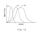
- FIG. 1A is a conceptual diagram of gain value adjustment
- FIG. 1B shows a conceptual diagram of offset value adjustment.
- the magnification of gain value is more than 1
- a luminance distribution A 2 can be obtained which is wider than a luminance distribution A 1 before adjustment.
- a luminance distribution A 3 can be obtained which is narrower than the luminance distribution A 1 before adjustment.
- the luminance contrast difference can be increased by adjusting the gain value.
- adjusting the offset value can shift the position of the luminance distribution without changing its width, as shown by the relationship between the luminance distribution A 1 before adjustment and a luminance distribution A 4 after adjustment.
- addition adjustment of the luminance can be made by adjusting the offset value.
- the adjusted image is generated by adjusting the gain value and the offset value of the before-adjustment image. Then, each of the gain value and the offset value of the adjusted image is varied in the predetermined increments or decrements. Thereafter, the difference in average luminance between the designated area and the comparison area is calculated for each combination of the gain value and the offset value (every time at least one of the gain value and the offset value is varied). The calculated differences in average luminance are compared with each other, and the adjusted image having the largest difference in average luminance is obtained as the optimal image.
- the gain value and the offset value are adjusted again so as to obtain the largest difference in average luminance between the designated area and the comparison area. This can increase the contrast between the designated area and the comparison area in the optimal image.
- the lighting apparatus may have a plurality of illumination units, the plurality of illumination units may have different incident angles of the illumination light on the imaging area from each other, and a plurality of the captured images may be obtained by the imaging apparatus for each of the plurality of illumination units.
- the incident angle of the illumination light is changed, the intensity of light that is reflected from the imaging area to the imaging apparatus is also changed, whereby the contrast of the captured image is changed.
- the plurality of incident angles of the illumination light there are the plurality of incident angles of the illumination light, and the number of incident angles is the same as that of the illumination units.
- the captured image is obtained at each of the plurality of incident angles. Thus, a high-contrast captured image can be more easily obtained.
- the plurality of illumination units may include an epi-illumination unit that emits the illumination light along a perpendicular line perpendicular to the imaging area, and an oblique-illumination unit that emits the illumination light from a direction crossing the perpendicular line.
- the illumination light can be emitted to the imaging area from the perpendicular direction perpendicular to the imaging area and the direction crossing the perpendicular direction.
- the plurality of color components may be three primary color components of red (R), green (G), and blue (B). According to this configuration, the contrast of the single-color images of any one of R, and B can be increased regardless of the color of the electronic component in the captured image. That is, the image generating apparatus according to this configuration can be adapted to a variety of colors of the electronic component.
- the electronic component may have a mark by which an orientation of the electronic component can be determined, and the mark may be included in the imaging area and the designated area.
- the orientation inspection can be performed on the electronic component placed on a tray or the electronic component mounted on a substrate, by using the optimal image.
- the accuracy of detecting wrong orientation of the electronic component is increased regardless of the operator's skill.
- the detection accuracy is less likely to vary, regardless of the operator's skill.
- the image generating apparatus may further include a display apparatus that displays the optimal image, wherein the image processing apparatus compares the average luminance of the designated area with that of the comparison area of the optimal image before display on the display apparatus, and the image processing apparatus sets the mark of the optimal image to be displayed on the display apparatus to white if the average luminance of the designated area is higher than that of the comparison area, and sets the mark of the optimal image to be displayed on the display apparatus to black if the average luminance of the designated area is lower than that of the comparison area.
- This configuration can further increase the contrast between the mark in the designated area and the comparison area. Thus, the mark can be more easily recognized.
- an image generating method includes the steps of: generating a before-adjustment image based on a captured image of an imaging area where at least a part of an electronic component is located; adjusting luminance of the before-adjustment image so as to generate an adjusted image; and setting a difference in average luminance between a designated area and a comparison area that is other than the designated area in the adjusted image largest so as to generate an optimal image.
- the image generating method includes the before-adjustment image generation step, the adjusted image generation step, and the optimal image generation step.
- the imaging area is first imaged to obtain the captured image.
- the before-adjustment image is generated by using as it is the captured image obtained by the imaging, or by performing image processing on the captured image as appropriate.
- the adjusted image is generated by adjusting the luminance of the before-adjustment image.
- the optimal image is generated by setting the difference in average luminance between the designated area and the comparison area in the adjusted image largest.
- the high-contrast optimal image optimal for detection of abnormalities etc. of the electronic component can be automatically generated from the captured image. Accordingly, the optimal image can be obtained in a shorter time as compared to the case where the optimal image is manually obtained by the operator. Moreover, the accuracy of detecting abnormalities of the electronic component is increased regardless of the operator's skill. Moreover, the detection accuracy is less likely to vary, regardless of the operator's skill.
- the before-adjustment image generation step may include the steps of: decomposing the captured image according to color components to generate a plurality of single-color images, and generating a plurality of selection candidate images based on the plurality of single-color images; and calculating the difference in average luminance between the designated area and the comparison area for each of the selection candidate images, and selecting a selected image having the largest difference in average luminance from the selection candidate images.
- the before-adjustment image may be the selected image.
- the before-adjustment image generation step includes the selection candidate image generation step and the image selection step.
- the selection candidate image generation step the captured image is first decomposed according to the color components to generate the plurality of single-color images.
- the plurality of selection candidate images are generated from the plurality of single-color images by using the plurality of single-color images as they are, or by synthesizing the plurality of single-color images as appropriate.
- the image selection step the difference in average luminance between the designated area and the comparison area is first calculated for each of the selection candidate images. Then, the selected image having the largest difference in average luminance is selected from the selection candidate images. This configuration can increase the contrast of the optimal image.
- the image generating method may further include the step of, after the optimal image generation step, generating the optimal image from another one of the captured images by using a condition obtained in the course from the before-adjustment image generation step to the optimal image generation step.
- the condition obtained in image processing performed earlier in time series can be used in image processing to be performed later in the time series. This reduces the time required for the later image processing.
- a luminance adjustment condition that is used to generate the adjusted image from the before-adjustment image in the adjusted image generation step can be used for both the electronic component that is subjected to the image processing earlier in the time series and the electronic component that is subjected to the image processing later in the time series.
- the adjusted image in the adjusted image generation step, may be generated by adjusting a gain value and an offset value of the before-adjustment image, and in the optimal image generation step, the optimal image having the largest difference in average luminance may be generated by varying each of the gain value and the offset value of the adjusted image in predetermined increments or decrements and calculating the difference in average luminance between the designated area and the comparison area for each combination of the gain value and the offset value.
- the adjusted image is generated by adjusting the gain value and the offset value of the before-adjustment image.
- each of the gain value and the offset value of the adjusted image is varied in the predetermined increments or decrements. Thereafter, the difference in average luminance between the designated area and the comparison area is calculated for each combination of the gain value and the offset value (every time at least one of the gain value and the offset value is varied). The calculated differences in average luminance are compared with each other, and the adjusted image having the largest difference in average luminance is obtained as the optimal image.
- the largest difference in average luminance between the designated area and the comparison area is obtained by adjusting the gain value and the offset value again. This can increase the contrast between the designated area and the comparison area in the optimal image.
- the electronic component may have a mark by which an orientation of the electronic component can be determined, and the mark may be included in the imaging area and the designated area.
- the orientation inspection can be performed on the electronic component placed on a tray or the electronic component mounted on a substrate, by using the optimal image.
- the accuracy of detecting wrong orientation of the electronic component is increased regardless of the operator's skill.
- the detection accuracy is less likely to vary, regardless of the operator's skill.
- the average luminance of the designated area may be compared with that of the comparison area in the optimal image, the mark of the optimal image may be set to white if the average luminance of the designated area is higher than that of the comparison area, and the mark of the optimal image may be set to black if the average luminance of the designated area is lower than that of the comparison area.
- This configuration can further increase the contrast between the mark in the designated area and the comparison area. Thus, the mark can be more easily recognized.
- an image generating apparatus and an image generating method can be provided which are capable of automatically generating a high-contrast optimal image from a captured image.
- FIG. 1A is a conceptual diagram of gain value adjustment
- FIG. 1B is a conceptual diagram of offset value adjustment
- FIG. 2 is a schematic diagram showing a substrate production line incorporating a substrate appearance inspection machine according to an embodiment of the present invention
- FIG. 3 is a top view of the substrate appearance inspection machine
- FIG. 4 is a perspective view of a portion near an inspection head of the substrate appearance inspection machine
- FIG. 5 is a top view of a substrate on which electronic components have been mounted
- FIG. 6 is a schematic diagram illustrating an image generating method according to an embodiment of the present invention.
- FIG. 7 is a perspective view of an electronic component mounting machine incorporating an image generating apparatus according to an embodiment of the present invention.
- FIG. 2 is a schematic diagram of a substrate production line having the substrate appearance inspection machine disposed therein.
- a substrate production line 9 includes a plurality of electronic component mounting machines 6 , a substrate appearance inspection machine 7 , and a reflow furnace 92 , sequentially from left (upstream) to right (downstream).
- the substrate appearance inspection machine 7 is interposed between the most downstream one of the electronic component mounting machines 6 and the reflow furnace 92 .
- a multiplicity of electronic components are mounted stepwise on a substrate that is transferred on the substrate production line 9 , by the plurality of electronic component mounting machines 6 .
- the substrate appearance inspection machine 7 inspects the mounting states of the electronic components on the substrate.
- the reflow furnace 92 melts cream solder interposed between the substrate and the electronic components to solder the electronic components to the substrate.
- FIG. 3 is a top view of the substrate appearance inspection machine 7 .
- a substrate B is shown hatched in FIG. 3 .
- the substrate appearance inspection machine 7 includes a base 72 , a substrate transfer apparatus 73 , an XY robot 74 , an inspection head 75 , a control apparatus 70 (see FIG. 2 ), an image processing apparatus 4 (see FIG. 2 ), and a display apparatus 5 (see FIG. 2 ).
- the substrate transfer apparatus 73 is disposed on the upper surface of the base 72 .
- the substrate transfer apparatus 73 includes a pair of front and rear conveyor belts 730 f , 730 r .
- the position and width of the substrate transfer apparatus 73 in the front-rear direction can be changed according to the position and width of transfer portions 660 f , 660 r of a substrate transfer apparatus 660 of the electronic component mounting machine 6 described later in the front-rear direction (see FIG. 7 ).
- the substrate B is transferred from left to right by the conveyor belts 730 f , 730 r .
- the conveyor belts 730 f , 730 r have a function as a substrate transfer device that transfers the substrate.
- the “X direction,” the “Y direction,” and the “Z direction” correspond to the left-right direction, the front-rear direction, and the up-down direction, respectively.
- the XY robot 74 includes a Y-direction slider 740 , an X-direction slider 741 , a pair of upper and lower Y-direction guide rails 742 , a pair of front and rear X-direction guide rails 743 f , 743 r , an X-direction movement ball screw portion 744 , and a Y-direction movement ball screw portion 745 .
- the pair of front and rear X-direction guide rails 743 f , 743 r are disposed on the upper surface of the base 72 such that the substrate transfer apparatus 73 is interposed therebetween in the front-rear direction.
- the X-direction slider 741 is attached to the pair of front and rear X-direction guide rails 743 f , 743 r so as to be slidable in the left-right direction.
- the X-direction slider 741 is driven by the X-direction movement ball screw portion 744 attached to the base 72 .
- the pair of upper and lower Y-direction guide rails 742 are disposed on the X-direction slider 741 .
- the Y-direction slider 740 is attached to the pair of upper and lower Y-direction guide rails 742 so as to be slidable in the front-rear direction.
- the Y-direction slider 740 is driven by the Y-direction movement ball screw portion 745 attached to the X-direction slider 741 .
- FIG. 4 is a perspective view of a portion near the inspection head 75 of the substrate appearance inspection machine 7 .
- the inspection head 75 includes a frame 750 , a lighting apparatus 2 , and an imaging apparatus 3 .
- the frame 750 includes three-stage brackets, namely upper, middle, and lower brackets 750 U, 750 M, and 750 D. Each of the brackets 750 U, 750 M, 750 D is provided, in the center thereof, with a hole that allows light to pass therethrough.
- the lighting apparatus 2 includes an epi-illumination unit 20 U, an upper oblique-illumination unit 20 M, and a lower oblique-illumination unit 20 D.
- the epi-illumination unit 20 U, the upper oblique-illumination unit 20 M, and the lower oblique-illumination unit 20 D are conceptually included in the “illumination unit” of the present invention.
- the epi-illumination unit 20 U is attached to the upper bracket 750 U.
- the epi-illumination unit 20 U includes a light source 200 U, a half mirror 201 U, and an optical system (not shown).
- light (illumination light) 21 U emitted from the light source 200 U is converted to parallel light by the optical system having a lens and the like.
- the emitted light 21 U travels leftward, changes its direction by 90° at the half mirror 201 U, and travels downward.
- an imaging area B 1 on the upper surface of the substrate B is irradiated with the emitted light 21 U from the direction directly above the imaging area B 1 .
- An incident angle ⁇ U of the emitted light 21 U on the imaging area B 1 is 90°.
- the upper oblique-illumination unit 20 M is attached to the middle bracket 750 M.
- the upper oblique-illumination unit 20 M includes a ring-shaped light source 200 M. As shown by dotted lines in FIG. 4 , the imaging area B 1 on the upper surface of the substrate B is irradiated with upper oblique light (illumination light) 21 M emitted from the light source 200 M from the direction of an incident angle ⁇ M ( ⁇ U).
- the lower oblique-illumination unit 20 D is attached to the lower bracket 750 D.
- the lower oblique-illumination unit 20 D includes a ring-shaped light source 200 D. As shown by dotted lines in FIG. 4 , the imaging area B 1 on the upper surface of the substrate B is irradiated with lower oblique light (illumination light) 21 D emitted from the light source 200 M from the direction of an incident angle ⁇ D ( ⁇ M).
- the light sources 200 U, 200 M, and 200 D are white light-emitting diodes (LEDs). Thus, each of the light sources 200 U, 200 M, and 200 D has all of three primary color components of red (R), green (G), and blue (B).
- the imaging apparatus 3 is attached to the upper bracket 750 U.
- the imaging apparatus 3 is a charge coupled device (CCD) area sensor.
- the imaging apparatus 3 has an imaging plane on which a multiplicity of light receiving elements are arranged two-dimensionally. The imaging apparatus 3 images the imaging area B 1 from the direction directly above the imaging area B 1 .
- the control apparatus 70 shown in FIG. 2 is capable of controlling in an integrated manner the substrate transfer apparatus 73 , the XY robot 74 , and the inspection head 75 , which are described above.
- the control apparatus 70 is electrically connected to the image processing apparatus 4 and the display apparatus 5 .
- An image generating apparatus 1 of the present embodiment is incorporated in the substrate appearance inspection machine 7 .
- the image generating apparatus 1 includes the lighting apparatus 2 , the imaging apparatus 3 , the image processing apparatus 4 , and the display apparatus 5 , out of the constituent members of the substrate appearance inspection machine 7 .
- the substrate on which electronic components have been mounted passes through the substrate appearance inspection machine 7 .
- the mounting state of the electronic components on the substrate is inspected here.
- FIG. 5 is a top view of the substrate on which the electronic components have been mounted. As shown in FIG. 5 , various electronic components P 1 to P 6 have been mounted on the substrate B. All the electronic components P 1 to P 6 are imaged by the imaging apparatus 3 shown in FIG. 4 in a predetermined order. Thus, the electronic components P 1 to P 6 are inspected for positional displacement or orientation displacement, or the electronic components P 1 to P 6 are inspected to see if there is any component missing.
- the orientation inspection the electronic component P 1 is inspected to check if the orientation of the electronic component P 1 matches a predetermined orientation (e.g., to check if the electronic component P 1 is properly mounted on the substrate B and not rotated 90° or 180°).
- the inspection head 75 shown in FIGS. 3 and 4 is moved to the position directly above the electronic component P 1 so that the electronic component P 1 is located in the imaging area B 1 .
- the epi-illumination unit 20 U, the upper oblique-illumination unit 20 M, and the lower oblique-illumination unit 20 D which are shown in FIG. 4 , are sequentially turned on, and the imaging area B 1 is imaged by the imaging apparatus 3 shown in FIG. 4 when each illumination unit is turned on. That is, a total of three images are obtained.
- the three images are processed by the image processing apparatus 4 shown in FIG. 2 .
- the orientation of the electronic component P 1 is inspected.
- an optimal image of the imaging area B 1 is generated through a before-adjustment image generation step (a selection candidate image generation step and an image selection step), an adjusted image generation step, and an optimal image generation step of an image generating method described below. Then, the orientation inspection is performed by using the optimal image.
- an optimal image of the imaging area B 1 is generated only through a condition utilization step of the image generating method described below. Then, the orientation inspection is performed by using the optimal image.
- the optimal image is displayed on the display apparatus (display) 5 . Whether the orientation of the electronic component is correct or not is automatically determined based on the average luminance of the optimal image, as described below.
- the inspected substrate is carried from the substrate appearance inspection machine 7 into the reflow furnace 92 , as shown in FIG. 2 .
- FIG. 6 is a schematic diagram illustrating the image generating method of the present embodiment.
- the image generating method of the present embodiment includes the before-adjustment image generation step, the adjusted image generation step, the optimal image generation step, and the condition utilization step (not shown).
- This step includes the selection candidate image generation step and the image selection step.
- the inspection head 75 shown in FIGS. 3 and 4 is first moved by the control apparatus 70 shown in FIG. 2 so that the electronic component P 1 shown in FIG. 5 is located in the imaging area B 1 shown in FIG. 4 .
- the epi-illumination unit 20 U shown in FIG. 4 is turned on by the control apparatus 70 shown in FIG. 2 . Then, with the emitted light 21 U being incident on the imaging area B 1 from directly thereabove, the imaging area B 1 is imaged by the imaging apparatus 3 . Thereafter, the epi-illumination unit 20 U shown in FIG. 4 is turned off and the upper oblique-illumination unit 20 M is turned on by the control apparatus 70 shown in FIG. 2 . Subsequently, with the upper oblique light 21 M being incident on the imaging area B 1 from an upper peripheral level, the imaging area B 1 is imaged by the imaging apparatus 3 . Then, the upper oblique-illumination unit 20 M shown in FIG.
- a designated area E 1 and a comparison area E 2 are set in each of the captured images D 1 to D 3 .
- the shape and size (the number of pixels: 8 bits) of the designated area E 1 are the same as those of the comparison area E 2 .
- a circular mark M is included in the designated area E 1
- the three captured images D 1 to D 3 are color images. Each of the captured images D 1 to D 3 is decomposed into three primary color components of R, and B. These primary color components are turned into data, and transmitted from the imaging apparatus 3 to the image processing apparatus 4 shown in FIG. 2 .
- the image processing apparatus 4 three single-color images D 1 R, D 1 G, and D 1 B of the three primary colors R, G, and B are generated from the captured image D 1 , three single-color images D 2 R, D 2 G, and D 2 B of the three primary colors R, G, and B are generated from the captured image D 2 , and three single-color images D 3 R, D 30 , and D 3 B of the three primary colors R, G, and B are generated from the captured image D 3 .
- a total of nine single-color images D 1 R, D 1 G, D 1 B, D 2 R, D 2 G, D 2 B, D 3 R, D 3 G, and D 3 B are generated in this manner.
- the nine single-color images D 1 R, D 1 G, D 1 B, D 2 R, D 2 G, D 2 B, D 3 R, D 3 G, and D 3 B are used as they are as selection candidate images.
- the difference in average luminance between the designated area E 1 and the comparison area E 2 is calculated for each of the nine single-color images D 1 R, D 1 G, D 1 B, D 2 R, D 2 G, D 2 B, D 3 R, D 3 G, and D 3 B.
- the luminance of each pixel in the designated area E 1 is detected, and a sum of the respective luminance values of the pixels is divided by the number of pixels in the designated area E 1 .
- the luminance of each pixel in the comparison area E 2 is detected, and a sum of the respective luminance values of the pixels is divided by the number of pixels in the comparison area E 2 .
- the average luminance of the designated area E 1 and the average luminance of the comparison area E 2 are calculated in this manner.
- the difference in average luminance between the designated area E 1 and the comparison area E 2 is calculated for each of the nine single-color images D 1 R, D 1 G, D 1 B, D 2 R, D 2 G; D 2 B, D 3 R, D 3 G, and D 3 B. Then, the single-color image (the single-color image D 1 R in this example) having the largest difference in average luminance is selected as a selected image F 1 R.
- a lookup table is first created. Specifically, the range of a gain value J is set to 0.00 to 255.00. The range of an offset value I is set to ⁇ 255 to 255.
- the offset value for the adjusted image K 1 R is varied in increments or decrements of 10 from ⁇ 200 to 200 while increasing the gain value in increments of 0.20 from 0.00 to 255.00.
- the difference in average luminance between the designated area E 1 and the comparison area E 2 is calculated for each combination of the gain value and the offset value. Note that the difference in average luminance is calculated by a method similar to that in the image selection step.
- gain value is 1.00 and the offset value is varied from ⁇ 200 to 200
- offset value is (1.00, ⁇ 200), (1.00, ⁇ 190), (1.00, ⁇ 180), . . . (1.00, 180), (1.00, 190), and (1.00, 200).
- the difference in average luminance between the designated area E 1 and the comparison area E 2 is calculated for each combination of the gain value and the offset value.
- gain value is 1.20 and the offset value is varied from ⁇ 200 to 200
- offset value is (1.20, ⁇ 200), (1.20, ⁇ 190), (1.20, ⁇ 180), . . . (1.20, 180), (1.20, 190), and (1.20, 200).
- the difference in average luminance between the designated area E 1 and the comparison area E 2 is calculated for each combination of the gain value and the offset value.
- the combination of the gain value and the offset value is selected which has the largest difference in average luminance. Note that if there are a plurality of combinations yielding the largest difference in average luminance, the combination having the smallest gain value is selected. The reason for this is that the larger the gain value is, the greater the influence of the individual differences is.
- image conversion is performed on the adjusted image K 1 R by using the selected combination of the gain value and the offset value, thereby generating an optimal image L 1 R having higher contrast between the designated area E 1 and the comparison area E 2 than the adjusted image K 1 R.
- the average luminance is compared between the designated area E 1 and the comparison area E 2 of the optimal image L 1 R by using the combination of the gain value and the offset value that yields the largest difference in average luminance. If the average luminance of the designated area E 1 is higher than that of the comparison area E 2 , the mark M of the optimal image L 1 R is set to white. On the other hand, if the average luminance of the designated area E 1 is lower than that of the comparison area E 2 , the mark M of the optimal image L 1 R is set to black.
- the optimal image L 1 R thus having the black or white mark M is displayed on the display apparatus 5 shown in FIG. 2 .
- Whether the orientation of the electronic component is correct or not is automatically determined.
- the image processing apparatus 4 compares the average luminance of the designated area E 1 with that of the comparison area E 2 in the optimal image L 1 R shown in FIG. 6 . It is herein assumed that the orientation shown in FIG. 6 is a correct mounting orientation of the electronic component P 1 .
- the average luminance in the designated area E 1 is higher than that of the comparison area E 2 , this means that the mark M having high luminance is present in the designated area E 1 .
- the series of steps described above namely the selection candidate image generation step, the image selection step, the adjusted image generation step, and the optimal image generation step, are performed on all of the electronic components P 1 to P 6 shown in FIG. 5 .
- the inspected substrate is carried from the substrate appearance inspection machine 7 into the reflow furnace 92 , as shown in FIG. 2 .
- the subsequent substrate to be inspected is transferred from the electronic component mounting machine 6 into the substrate appearance inspection machine 7 .
- the electronic components on the new substrate are inspected by utilizing as they are the conditions obtained by the series of steps described above, namely the selection candidate image generation step, the image selection step, the adjusted image generation step, and the optimal image generation step.
- the new substrate is of the same kind as the inspected substrate. That is, as shown in FIG. 5 , the same electronic components P 1 to P 6 are mounted at the same coordinates on both the new substrate B and the inspected substrate B. Thus, the conditions for the electronic component P 1 on the inspected substrate B can be used as they are for the electronic component P 1 on the new substrate B. The same applies to the electronic components P 2 to P 6 .
- inspection of the orientation of the electronic component P 1 on the new substrate B will be described below by comparing with the inspection of the orientation of the electronic component P 1 on the inspected substrate B described above.
- the only one captured image D 1 is obtained in this step. That is, the imaging conditions of the captured image D 1 are utilized which have been set in the selection candidate image generation step performed on the inspected substrate.
- the imaging conditions are conceptually included in the “condition” in the present invention. Specifically, the epi-illumination unit 20 U shown in FIG. 4 is turned on, and the imaging area B 1 is imaged by using the imaging apparatus 3 .
- the reason why the only one captured image D 1 is obtained is that, as shown in FIG. 6 , it has already been known from the result of the selection candidate image generation step and the image selection step performed on the inspected substrate that the single-color image D 1 R obtained from the captured image D 1 is going to be selected as the selected image F 1 R.
- the single-color image D 1 R is selected as it is as the selected image F 1 R.
- the lookup table created in the adjusted image generation step performed on the inspected substrate is used in this step.
- the lookup table is conceptually included in the “condition” in the present invention. That is, image conversion is performed on the selected image F 1 R by using the lookup table.
- the adjusted image K 1 R is generated which has higher contrast between the designated area E 1 and the comparison area E 2 than the selected image F 1 R.
- a combination of the gain value and the offset value that yields the largest difference in average luminance is used.
- This combination is the combination obtained in the optimal image generation step performed on the inspected substrate.
- the combination of the gain value and the offset value that yields the largest difference in average luminance is conceptually included in the “condition” in the present invention. That is, image conversion is performed on the adjusted image K 1 R by using this combination of the gain value and the offset value.
- the optimal image L 1 R is generated which has higher contrast between the designated area E 1 and the comparison area E 2 than the adjusted image K 1 R.
- the optimal image L 1 R having the white mark M is displayed on the display apparatus 5 shown in FIG. 2 .
- whether the orientation of the electronic component is correct or not is automatically determined.
- the condition utilization step is performed on all of the electronic components P 1 to P 6 shown in FIG. 5 .
- the inspected substrate is carried from the substrate appearance inspection machine 7 into the reflow furnace 92 , as shown in FIG. 2 .
- the subsequent substrate to be inspected is transferred from the electronic component mounting machine 6 to the substrate appearance inspection machine 7 .
- the condition utilization step is also performed on this substrate.
- the condition utilization step is sequentially repeatedly performed on the substrates of the same kind.
- the image generating apparatus 1 and the image generating method of the present embodiment As shown in FIG. 6 , the high-contrast optimal image L 1 R that is optimal for detection of abnormalities etc. of the electronic components P 1 to P 6 can be automatically generated from the captured images D 1 to D 3 .
- the optimal image L 1 R can be obtained in a shorter time as compared to the case where the optimal image L 1 R is manually obtained by the operator.
- the accuracy of detecting abnormalities of the electronic components P 1 to P 6 is increased regardless of the operator's skill.
- the detection accuracy is less likely to vary, regardless of the operator's skill.
- the conditions obtained when the selection candidate image generation step, the image selection step, the adjusted image generation step, and the optimal image generation step are performed on the first substrate can be used as they are for the second and subsequent substrates.
- the condition utilization step can be repeatedly performed on the second and subsequent substrates.
- the conditions obtained in the orientation inspection of the electronic components P 1 to P 6 on the first substrate can be utilized as they are in the orientation inspection of the electronic components P 1 to P 6 on the second and subsequent substrates. This reduces the time required for the image processing and therefore for the orientation inspection of the electronic components P 1 to P 6 .
- the gain value and the offset value are adjusted in the adjusted image generation step so as to generate the adjusted image K 1 R from the selected image F 1 R.
- the gain value and the offset value are adjusted again so as to generate the optimal image L 1 R from the adjusted image K 1 R. This can increase the contrast between the designated area E 1 and the comparison area E 2 in the optimal image L 1 R.
- the lighting apparatus 2 includes the epi-illumination unit 20 U, the upper oblique-illumination unit 20 M, and the lower oblique-illumination unit 20 D.
- the incident angle ⁇ U of the light 21 U emitted from the epi-illumination unit 20 U, the incident angle ⁇ M of the upper oblique light 21 M from the upper oblique-illumination unit 20 M, and the incident angle ⁇ D of the lower oblique light 21 D from the lower oblique-illumination unit 20 D are different from each other.
- the captured image D 6 shown in FIG. 6 is captured by the imaging apparatus 3 when the imaging area B 1 is irradiated with the emitted light 21 U.
- the captured image D 2 shown in FIG. 6 is captured by the imaging apparatus 3 when the imaging area B 1 is irradiated with the upper oblique light 21 M.
- the captured image D 3 shown in FIG. 6 is captured by the imaging apparatus 3 when the imaging area B 1 is irradiated with the lower oblique light 21 D.
- the contrast varies among the captured images D 1 to D 3 . This makes it easier to obtain the captured image D 1 to D 3 having high contrast.
- the single-color images D 1 R, D 1 G, D 1 B, D 2 R, D 2 G, D 2 B, D 3 R, D 3 G, and D 3 B of the three primary colors R, G, and B are generated, as shown in FIG. 6 .
- the contrast of the single-color images D 1 R, D 1 G, D 1 B, D 2 R, D 2 G, D 2 B, D 3 R, D 3 G, D 3 B of any one of R, G, and B can be increased regardless of the color of the electronic components P 1 to P 6 in the captured images D 1 to D 3 . That is, the image generating apparatus 1 and the image generating method of the present embodiment can be adapted to a variety of colors of the electronic components P 1 to P 6 .
- the mark M in the optimal image L 1 R that is displayed on the display apparatus 5 is set to white or black according to the average luminance values of the designated area E 1 and the comparison area E 2 . This can further increase the contrast between the mark M in the designated area E 1 and the comparison area E 2 . Thus, the mark M can be more easily recognized.
- FIG. 7 is a perspective view of the electronic component mounting machine 6 incorporating the image generating apparatus according to the embodiment of the present invention.
- the electronic component mounting machine 6 includes a base 65 , a module 66 , a tray unit 67 , a device pallet 63 , a control apparatus 60 (see FIG. 2 ), an image processing apparatus 61 (see FIG. 2 ), and a display apparatus 62 (see FIG. 2 ).
- the module 66 is detachably provided on the upper surface of the base 65 .
- the module 66 includes the substrate transfer apparatus 660 , an XY robot 661 , a mount head 662 , a mark camera 663 , a part camera 64 , and a lighting apparatus (not shown).
- the substrate transfer apparatus 660 includes the pair of front and rear transfer portions 660 f , 660 r .
- the mark camera 663 is conceptually included in the “imaging apparatus” of the present invention.
- Each of the transfer portions 660 f , 660 r includes a pair of conveyor belts. Each of the transfer portions 660 f , 660 r is capable of transferring the substrate B.
- the XY robot 661 includes a Y-direction slider 661 a , an X-direction slider 661 b , a pair of right and left Y-direction guide rails 661 c , and a pair of upper and lower X-direction guide rails 661 d .
- the pair of right and left Y-direction guide rails 661 c are disposed on the upper surface of the inner space of a housing of the module 66 .
- the Y-direction slider 661 a is attached to the pair of right and left Y-direction guide rails 661 c so as to be slidable in the front-rear direction.
- the pair of upper and lower X-direction guide rails 661 d are disposed on the front surface of the Y-direction slider 661 a .
- the X-direction slider 661 b is attached to the pair of upper and lower X-direction guide rails 661 d so as to be slidable in the left-right direction.
- the mount head 662 is attached to the X-direction slider 661 b .
- the mount head 662 is movable in the front-rear and left-right directions by the XY robot 661 .
- a suction nozzle 662 a is attached to a lower portion of the mount head 662 .
- the suction nozzle 662 a is movable downward with respect to the mount head 662 .
- the mark camera 663 and the lighting apparatus (white LED), together with the mount head 662 , are attached to the X-direction slider 661 .
- the mark camera 663 and the lighting apparatus (white LED) are movable in the front-rear and left-right directions by the XY robot 661 .
- the mark camera 663 is capable of imaging the substrate B and an alignment mark on the electronic component.
- the lighting apparatus is capable of emitting illumination light to an imaging area of the mark camera 663 .
- the part camera 64 is disposed in front of the transfer portion 660 f .
- the suction nozzle 662 a i.e., the mount head 662 ) that has picked up the electronic component by suction passes above the part camera 64 . At this time, the electronic component on the suction nozzle 662 a is imaged by the part camera 64 .
- the device pallet 63 is mounted in a front opening of the module 66 .
- the tray unit 67 is disposed in front of the base 65 .
- the tray unit 67 includes a case 670 and a shuttle conveyor 671 .
- a plurality of trays 672 are stacked in the up-down direction in the case 670 .
- the rear end of the shuttle conveyor 671 reaches the upper edge of the device pallet 63 .
- the trays 672 in the case 670 are capable of being drawn rearward (in the direction toward the substrate B) by the shuttle conveyor 671 .
- the image generating apparatus 1 of the present embodiment is incorporated in the electronic component mounting machine 6 .
- the image generating apparatus 1 includes the lighting apparatus, the mark camera 663 , the image processing apparatus 61 , and the display apparatus 62 out of the constituent members of the electronic component mounting machine 6 .
- Electronic components are placed on the trays 672 . Each electronic component is transferred by the suction nozzle 662 a from the tray 672 to the mounting coordinates on the substrate B via the part camera 64 . The electronic component is mounted at the mounting coordinates on the substrate B by the suction nozzle 662 a.
- the orientation of the electronic component placed on the tray 672 may not match a predetermined orientation.
- the electronic component P 1 may be mounted so as to be rotated 90° or 180° with respect to the predetermined orientation.
- the orientation of the electronic component on the tray 672 may be inspected before the orientation inspection is performed in the substrate appearance inspection machine 7 shown in FIG. 2 .
- the control apparatus 60 performs the operation of the control apparatus 70 shown in FIG. 2
- the image processing apparatus 61 performs the operation of the image processing apparatus 4 shown in FIG. 2
- the display apparatus 62 performs the operation of the display apparatus 5 shown in FIG. 2
- the mark camera 663 shown in FIG. 7 performs the operation of the imaging apparatus 3 shown in FIG. 4
- the lighting apparatus provided together with the mark camera 663 performs the operation of the lighting apparatus 2 shown in FIG. 4 .
- Incorporating the image generating apparatus 1 in the electronic component mounting machine 6 can increase the contrast of the image of the electronic component on the tray 672 . Thus, the accuracy of detecting wrong orientation of the electronic component can be increased.
- the part camera 64 may be used as the imaging apparatus of the image generating apparatus 1 .
- the lighting apparatus (not shown) provided together with the part camera 64 may be used as the lighting apparatus of the image generating apparatus 1 . This can increase the contrast of the image of the electronic component sucked by the suction nozzle 662 a . Thus, the accuracy of detecting wrong orientation of the electronic component can be increased.
- white LEDs are used as the light sources 200 U, 200 M, and 200 D, as shown in FIG. 4 .
- single-color LEDs of R, G, and B may be used in combination as the light sources 200 U, 200 M, and 200 D.
- Other illumination units such as a fluorescent lamp may be used.
- the light sources 200 M, 200 D need not necessarily have a ring shape (an endless annular shape).
- the light sources 200 M, 200 D may have a dot shape or a partial arc shape.
- the three illumination units namely the epi-illumination unit 20 U, the upper oblique-illumination unit 20 M, and the lower oblique-illumination unit 20 D, are provided in the lighting apparatus 2 .
- the number of illumination units is not particularly limited. If the number of illumination units is one, disposing the illumination unit so as to be movable with respect to the imaging apparatus 3 allows the incident angle of the illumination light to be switched as appropriate among ⁇ U, ⁇ M, and ⁇ D.
- the three captured images D 1 to D 3 are obtained by the imaging apparatus 3 in the selection candidate image generation step.
- the number of captured images D 1 to D 3 is not particularly limited.
- the plurality of single-color images D 1 R, D 1 G, D 1 B, D 2 R, D 2 G, D 2 B, D 3 R, D 3 G, and D 3 B can be generated even if the number of captured images D 1 to D 3 is one.
- the single-color images D 1 R, D 1 G, D 1 B, D 2 R, D 2 G, D 2 B, D 3 R, D 3 G, and D 3 B are generated from the captured images D 1 to D 3
- the selected image F 1 R is generated from the single-color images D 1 R, D 1 G, D 1 B, D 2 R, D 2 G, D 2 B, D 3 R, D 3 G, and D 3 B in the before-adjustment image generation step.
- the captured image D 1 to D 3 may be used as it is as the before-adjustment image (the selected image) F 1 R. This reduces the time required for image processing.
- the color components of the single-color images D 1 R, D 1 G, D 1 B, D 2 R, D 2 G, D 2 B, D 3 R, D 3 G, and D 3 B are not particularly limited.
- the captured images D 1 to D 3 need not necessarily be color images.
- the single-color images D 1 R, D 1 G, D 1 B, D 2 R, D 2 G, D 2 B, D 3 R, D 3 G, and D 3 B are used as they are as the selection candidate images in the selection candidate image generation step.
- an image obtained by synthesizing the single-color images D 1 R, D 1 G, D 1 B, D 2 R, D 2 G, D 2 B, D 3 R, D 3 G, and D 3 B as appropriate may be used as the selection candidate image.
- the single-color images D 1 R, D 1 G, D 1 B, D 2 R, D 2 G, D 2 B, D 3 R, D 3 G, and D 3 B need only be synthesized so as to increase the contrast between the designated area E 1 and the comparison area E 2 in the selected candidate image.
- the number of single-color images D 1 R, D 1 G, D 1 B, D 2 R, D 2 G, D 2 B, D 3 R, D 3 G, and D 3 B to be synthesized (how many of the single-color images D 1 R, D 1 G, D 1 B, D 2 R, D 2 G, D 2 B, D 3 R, D 3 G, and D 3 B are synthesized to generate a single selection candidate image) is not particularly limited.
- the number of selection candidate images to be generated is not particularly limited.
- the orientation inspection is performed by using the circular mark M on the electronic component P 1 .
- the mark M for use in the orientation inspection is not particularly limited.
- a character, a number, a model number, etc. on the electronic component P 2 , a semicircular pattern on the electronic component P 3 , a trapezoidal pattern on the electronic component P 4 , a quadrangular pattern on the electronic component P 5 , a linear pattern on the electronic component P 6 , etc. may be used as the mark M.
- a shape feature of the electronic component may be used as the mark M.
- the designated area E 1 and the comparison area E 2 are arranged diagonally.
- the positional relationship between the designated area E 1 and the comparison area E 2 is not particularly limited.
- the designated area E 1 and the comparison area E 2 need only be arranged so as to increase the contrast between the designated area E 1 and the comparison area E 2 .
- the lookup table is created by using the expressions (1) and (2) in the adjusted image generation step. That is, the image modulation (enhancement) is performed by using the expressions (1) and (2). However, the image modulation may be performed by using a modulation expression other than the expressions (1) and (2).
- the range of the gain value J and the range of the offset value I which are set when creating the lookup table are not particularly limited.
- the increments of the variable x in the expression (2) are not particularly limited.
- the difference in average luminance between the designated area E 1 and the comparison area E 2 is calculated for each combination of the gain value and the offset value by varying the gain value and the offset value for the adjusted image K 1 R in the optimal image generation step.
- the increments or decrements of the gain value and the offset value are not particularly limited. If there are a plurality of combinations of the gain value and the offset value that yield the largest difference in average luminance, a combination of the gain value and the offset value that has the smallest gain value need not necessarily be selected.
- the orientation of the electronic component P 1 is automatically determined by comparing the average luminance of the designated area E 1 with that of the comparison area E 2 of the optimal image L 1 R by the image processing apparatus 4 .
- the orientation of the electronic component P 1 may be visually determined by the operator by looking at the screen of the display apparatus 5 .
- the mark M in the optimal image L 1 R that is displayed on the display apparatus 5 is set to white or black according to the respective average luminance values of the designated area E 1 and the comparison area E 2 . This makes it easier for the operator to determine the orientation of the electronic component P 1 .
- the image processing apparatus 4 may set intermediate luminance (which need not necessarily be a median value) between the average luminance of the designated area E 1 and the average luminance of the comparison area E 2 of the optimal image L 1 R as a threshold value.
- the orientation of the electronic component P 1 may be inspected by using this threshold value.
- this threshold value may be used for the orientation inspection of the subsequent electronic component.
- the threshold value is conceptually included in the “condition” in the present invention.
- the before-adjustment image generation step (the selection candidate image generation step and the image selection step), the adjusted image generation step, and the optimal image generation step in the image processing method are performed on the first substrate B transferred to the substrate appearance inspection machine 7 .
- these steps may be performed outside the substrate production line 9 , and the substrate appearance inspection machine 7 may inspect the orientation of the electronic component on the first substrate B transferred thereto, by utilizing the same conditions obtained by these steps.
- an imaging environment similar to that of the substrate appearance inspection machine 7 such as that shown in FIG. 4 , need be provided outside the substrate production line 9 .
- control apparatus 70 and the image processing apparatus 4 of the substrate appearance inspection machine 7 are separately disposed.
- control apparatus 70 and the image processing apparatus 4 of the substrate appearance inspection machine 7 may be integrally disposed by using a common computer or the like.
- control apparatus 60 and the image processing apparatus 61 of the electronic component mounting machine 6 may be integrally disposed.
- the substrate appearance inspection machine 7 is disposed upstream of the reflow furnace 92 in the above embodiment, the substrate appearance inspection machine 7 may be provided downstream of the reflow furnace 92 .
- the orientation inspection is individually performed on the electronic components P 1 to P 6 .
- the orientation inspection may be performed on two or more of the electronic components P 1 to P 6 at a time by using the imaging apparatus 3 having a large imaging area B 1 . This reduces the time required for the orientation inspection.
- the image generating apparatus and the image generating method according to the present invention are used for the orientation inspection of the electronic components.
- the image generating apparatus and the image generating method according to the present invention may be used to inspect the electronic components for positional displacement, or to inspect to see if there is any component missing.
Landscapes
- Engineering & Computer Science (AREA)
- Operations Research (AREA)
- Manufacturing & Machinery (AREA)
- Microelectronics & Electronic Packaging (AREA)
- Physics & Mathematics (AREA)
- Health & Medical Sciences (AREA)
- Life Sciences & Earth Sciences (AREA)
- Chemical & Material Sciences (AREA)
- Analytical Chemistry (AREA)
- Biochemistry (AREA)
- General Health & Medical Sciences (AREA)
- General Physics & Mathematics (AREA)
- Immunology (AREA)
- Pathology (AREA)
- Image Processing (AREA)
- Image Analysis (AREA)
- Investigating Materials By The Use Of Optical Means Adapted For Particular Applications (AREA)
Abstract
Description
H=127.5−I×0.5 (1)
J=((x−H)×J+H+0.5)+I (2)
Claims (14)
Applications Claiming Priority (2)
| Application Number | Priority Date | Filing Date | Title |
|---|---|---|---|
| JP2010-290605 | 2010-12-27 | ||
| JP2010290605A JP5877639B2 (en) | 2010-12-27 | 2010-12-27 | Image generating apparatus and image generating method |
Publications (2)
| Publication Number | Publication Date |
|---|---|
| US20120162405A1 US20120162405A1 (en) | 2012-06-28 |
| US9474195B2 true US9474195B2 (en) | 2016-10-18 |
Family
ID=46316211
Family Applications (1)
| Application Number | Title | Priority Date | Filing Date |
|---|---|---|---|
| US13/334,656 Active 2035-08-18 US9474195B2 (en) | 2010-12-27 | 2011-12-22 | Image generating apparatus and image generating method |
Country Status (3)
| Country | Link |
|---|---|
| US (1) | US9474195B2 (en) |
| JP (1) | JP5877639B2 (en) |
| CN (1) | CN102595870B (en) |
Families Citing this family (14)
| Publication number | Priority date | Publication date | Assignee | Title |
|---|---|---|---|---|
| JP2012068162A (en) * | 2010-09-24 | 2012-04-05 | Renesas Electronics Corp | Method, apparatus, and program for processing contrast image of semiconductor device |
| WO2014033815A1 (en) * | 2012-08-27 | 2014-03-06 | 富士機械製造株式会社 | Ng component display method and ng component display system |
| CN107535090B (en) * | 2015-05-21 | 2020-09-01 | 株式会社富士 | Device and method for generating component orientation determination data |
| JP6526514B2 (en) * | 2015-07-31 | 2019-06-05 | リコーエレメックス株式会社 | Inspection apparatus, method and program |
| JP6528133B2 (en) * | 2016-03-04 | 2019-06-12 | パナソニックIpマネジメント株式会社 | Component mounting device |
| CN107330867B (en) * | 2017-06-16 | 2020-02-18 | Oppo广东移动通信有限公司 | Image synthesis method, apparatus, computer-readable storage medium, and computer device |
| JP7094282B2 (en) * | 2017-06-21 | 2022-07-01 | 株式会社Fuji | Anti-board work equipment |
| CN111373852B (en) * | 2017-12-04 | 2021-10-22 | 株式会社富士 | Electronic component mounting direction confirmation system and electronic component mounting direction confirmation method |
| US11546528B2 (en) * | 2018-07-12 | 2023-01-03 | Fuji Corporation | Image processing method |
| JP7281942B2 (en) * | 2019-03-29 | 2023-05-26 | Juki株式会社 | Inspection device and inspection method |
| WO2020255365A1 (en) * | 2019-06-21 | 2020-12-24 | 株式会社Fuji | Image synthesis device, image acquisition device, image processing system, and image processing method |
| JP7197705B2 (en) * | 2019-07-19 | 2022-12-27 | 株式会社Fuji | Mounting equipment, mounting system, and inspection mounting method |
| US12051188B2 (en) * | 2019-07-26 | 2024-07-30 | Fuji Corporation | Substrate work system |
| JP7561519B2 (en) * | 2020-05-22 | 2024-10-04 | 株式会社アマダ | Bending system and method of using same |
Citations (9)
| Publication number | Priority date | Publication date | Assignee | Title |
|---|---|---|---|---|
| JPH08219716A (en) | 1994-12-13 | 1996-08-30 | Toshiba Corp | Input image contrast processing device and device using the same |
| JP2000099625A (en) | 1998-09-28 | 2000-04-07 | Nidek Co Ltd | Character recognizing device |
| WO2000067005A1 (en) | 1999-05-04 | 2000-11-09 | Speedline Technologies, Inc. | A method and apparatus for inspecting solder paste deposits on substrates |
| JP2003066339A (en) | 2001-08-29 | 2003-03-05 | Olympus Optical Co Ltd | Image comparison device |
| CN1747647A (en) | 2005-08-05 | 2006-03-15 | 华南理工大学 | Self-adaptive light-source illuminating system and method for paster |
| JP2006200900A (en) | 2005-01-18 | 2006-08-03 | Juki Corp | Object recognition method and apparatus |
| JP2006300888A (en) | 2005-04-25 | 2006-11-02 | Anritsu Sanki System Co Ltd | Density data conversion method and apparatus, and X-ray inspection system |
| JP2009076796A (en) | 2007-09-24 | 2009-04-09 | Fuji Mach Mfg Co Ltd | Electronic component orientation inspection apparatus, electronic component orientation inspection method, and electronic component placement machine |
| JP2009236493A (en) | 2008-03-25 | 2009-10-15 | Mitsubishi Rayon Co Ltd | Flaw inspecting method of transparent plate and flaw inspection device |
-
2010
- 2010-12-27 JP JP2010290605A patent/JP5877639B2/en active Active
-
2011
- 2011-12-22 US US13/334,656 patent/US9474195B2/en active Active
- 2011-12-27 CN CN201110457105.6A patent/CN102595870B/en active Active
Patent Citations (10)
| Publication number | Priority date | Publication date | Assignee | Title |
|---|---|---|---|---|
| JPH08219716A (en) | 1994-12-13 | 1996-08-30 | Toshiba Corp | Input image contrast processing device and device using the same |
| JP2000099625A (en) | 1998-09-28 | 2000-04-07 | Nidek Co Ltd | Character recognizing device |
| WO2000067005A1 (en) | 1999-05-04 | 2000-11-09 | Speedline Technologies, Inc. | A method and apparatus for inspecting solder paste deposits on substrates |
| JP2002543421A (en) | 1999-05-04 | 2002-12-17 | スピードライン・テクノロジーズ・インコーポレーテッド | Method and apparatus for inspecting solder paste deposition on a substrate |
| JP2003066339A (en) | 2001-08-29 | 2003-03-05 | Olympus Optical Co Ltd | Image comparison device |
| JP2006200900A (en) | 2005-01-18 | 2006-08-03 | Juki Corp | Object recognition method and apparatus |
| JP2006300888A (en) | 2005-04-25 | 2006-11-02 | Anritsu Sanki System Co Ltd | Density data conversion method and apparatus, and X-ray inspection system |
| CN1747647A (en) | 2005-08-05 | 2006-03-15 | 华南理工大学 | Self-adaptive light-source illuminating system and method for paster |
| JP2009076796A (en) | 2007-09-24 | 2009-04-09 | Fuji Mach Mfg Co Ltd | Electronic component orientation inspection apparatus, electronic component orientation inspection method, and electronic component placement machine |
| JP2009236493A (en) | 2008-03-25 | 2009-10-15 | Mitsubishi Rayon Co Ltd | Flaw inspecting method of transparent plate and flaw inspection device |
Non-Patent Citations (5)
| Title |
|---|
| Aug. 19, 2014 Office Action issued in Japanese Application No. 2010-290605 (with translation). |
| Jun. 8, 2015 Office Action issued in Chinese Application No. 201110457105.6. |
| Masumura, Shigeki, "Writing Technology for Image Processing System and the Prospect," Eiziojoho Industrial, vol. 34, No. 1, pp. 29-36, Jan. 2002. |
| Oct. 28, 2014 Office Action issued in Japanese Application No. 2010-290605 (with translation). |
| Okuda, Kenji et al., "IC Character Reading Machine," Toshiba Review, vol. 52, No. 2, pp. 55-58, Feb. 1, 1997 (with abstract). |
Also Published As
| Publication number | Publication date |
|---|---|
| CN102595870B (en) | 2016-08-31 |
| JP5877639B2 (en) | 2016-03-08 |
| JP2012137980A (en) | 2012-07-19 |
| US20120162405A1 (en) | 2012-06-28 |
| CN102595870A (en) | 2012-07-18 |
Similar Documents
| Publication | Publication Date | Title |
|---|---|---|
| US9474195B2 (en) | Image generating apparatus and image generating method | |
| JP6109317B2 (en) | Substrate production operation method, substrate imaging condition determination method, and substrate production operation apparatus | |
| US10416086B2 (en) | Image inspection device | |
| US9970745B2 (en) | Measurement target measuring program, measurement target measuring method, and magnifying observation device | |
| US8363929B2 (en) | Shape measurement apparatus and calibration method | |
| US20180330489A1 (en) | Image Inspection Device | |
| JP5338773B2 (en) | Component mounting apparatus, imaging illumination apparatus, and illumination method | |
| US11734812B2 (en) | Fused imaging device and method | |
| US11763442B2 (en) | Fused imaging device and method | |
| JP5338772B2 (en) | Component mounting apparatus, imaging illumination apparatus, and illumination method | |
| US11971367B2 (en) | Inspection device and inspection method | |
| JP4315752B2 (en) | Electronic component mounting equipment | |
| JP5913866B2 (en) | Master data creation method for board inspection | |
| JP4309221B2 (en) | Electronic component mounting equipment | |
| US11575814B2 (en) | Image capturing device and appearance inspecting device including the same | |
| US11997375B2 (en) | Image correction method, imaging device, and inspection device | |
| JP2008275487A (en) | Shape inspection apparatus and shape inspection method | |
| JP7562860B2 (en) | Component Mounting Machine | |
| CN121128160A (en) | Image display system and image display method | |
| JP2006294806A (en) | Illumination setting method, illumination setting device, and component transfer device | |
| WO2024009410A1 (en) | Component presence/absence determination method and image processing system | |
| JP2014055913A (en) | Appearance inspection device, and control method and program of appearance inspection device | |
| JP2008112931A (en) | Electronic component mounting device | |
| JP2021125487A (en) | Board inspection device, board inspection method | |
| JP2002175518A (en) | Image recognition device and image recognition method |
Legal Events
| Date | Code | Title | Description |
|---|---|---|---|
| AS | Assignment |
Owner name: FUJI MACHINE MFG. CO., LTD., JAPAN Free format text: ASSIGNMENT OF ASSIGNORS INTEREST;ASSIGNORS:INAGAKI, MITSUTAKA;SUZUKI, IKUO;OIKE, HIROSHI;SIGNING DATES FROM 20111207 TO 20111208;REEL/FRAME:027494/0306 |
|
| STCF | Information on status: patent grant |
Free format text: PATENTED CASE |
|
| AS | Assignment |
Owner name: FUJI CORPORATION, JAPAN Free format text: CHANGE OF NAME;ASSIGNOR:FUJI MACHINE MFG. CO., LTD.;REEL/FRAME:046959/0082 Effective date: 20180402 |
|
| MAFP | Maintenance fee payment |
Free format text: PAYMENT OF MAINTENANCE FEE, 4TH YEAR, LARGE ENTITY (ORIGINAL EVENT CODE: M1551); ENTITY STATUS OF PATENT OWNER: LARGE ENTITY Year of fee payment: 4 |
|
| MAFP | Maintenance fee payment |
Free format text: PAYMENT OF MAINTENANCE FEE, 8TH YEAR, LARGE ENTITY (ORIGINAL EVENT CODE: M1552); ENTITY STATUS OF PATENT OWNER: LARGE ENTITY Year of fee payment: 8 |