US9469522B2 - Epi-poly etch stop for out of plane spacer defined electrode - Google Patents
Epi-poly etch stop for out of plane spacer defined electrode Download PDFInfo
- Publication number
- US9469522B2 US9469522B2 US14/201,453 US201414201453A US9469522B2 US 9469522 B2 US9469522 B2 US 9469522B2 US 201414201453 A US201414201453 A US 201414201453A US 9469522 B2 US9469522 B2 US 9469522B2
- Authority
- US
- United States
- Prior art keywords
- layer
- etch stop
- cap layer
- oxide layer
- electrode
- Prior art date
- Legal status (The legal status is an assumption and is not a legal conclusion. Google has not performed a legal analysis and makes no representation as to the accuracy of the status listed.)
- Active, expires
Links
- 125000006850 spacer group Chemical group 0.000 title claims description 10
- 238000005530 etching Methods 0.000 claims abstract description 27
- 238000000034 method Methods 0.000 claims abstract description 26
- 238000000151 deposition Methods 0.000 claims abstract description 25
- 239000000463 material Substances 0.000 claims abstract description 23
- 229910052581 Si3N4 Inorganic materials 0.000 claims description 2
- HQVNEWCFYHHQES-UHFFFAOYSA-N silicon nitride Chemical compound N12[Si]34N5[Si]62N3[Si]51N64 HQVNEWCFYHHQES-UHFFFAOYSA-N 0.000 claims description 2
- 238000005137 deposition process Methods 0.000 claims 1
- 150000004767 nitrides Chemical class 0.000 description 52
- 235000012431 wafers Nutrition 0.000 description 45
- 238000002161 passivation Methods 0.000 description 14
- 238000002955 isolation Methods 0.000 description 13
- 230000008569 process Effects 0.000 description 12
- 230000008021 deposition Effects 0.000 description 11
- 229910052710 silicon Inorganic materials 0.000 description 7
- 239000010703 silicon Substances 0.000 description 7
- XUIMIQQOPSSXEZ-UHFFFAOYSA-N Silicon Chemical compound [Si] XUIMIQQOPSSXEZ-UHFFFAOYSA-N 0.000 description 6
- 238000004891 communication Methods 0.000 description 5
- 239000011810 insulating material Substances 0.000 description 5
- 229910021420 polycrystalline silicon Inorganic materials 0.000 description 5
- 230000026683 transduction Effects 0.000 description 5
- 238000010361 transduction Methods 0.000 description 5
- 229920005591 polysilicon Polymers 0.000 description 4
- 239000000758 substrate Substances 0.000 description 4
- 230000008901 benefit Effects 0.000 description 3
- 238000011049 filling Methods 0.000 description 3
- 239000002184 metal Substances 0.000 description 3
- 230000004048 modification Effects 0.000 description 3
- 238000012986 modification Methods 0.000 description 3
- 229920002120 photoresistant polymer Polymers 0.000 description 3
- 238000005538 encapsulation Methods 0.000 description 2
- 230000004927 fusion Effects 0.000 description 2
- 238000004519 manufacturing process Methods 0.000 description 2
- 229910021421 monocrystalline silicon Inorganic materials 0.000 description 2
- 238000005498 polishing Methods 0.000 description 2
- 238000007142 ring opening reaction Methods 0.000 description 2
- RGTYLICFMNSKMS-UHFFFAOYSA-N [Si].[Si].[Si] Chemical compound [Si].[Si].[Si] RGTYLICFMNSKMS-UHFFFAOYSA-N 0.000 description 1
- 230000004075 alteration Effects 0.000 description 1
- QVGXLLKOCUKJST-UHFFFAOYSA-N atomic oxygen Chemical compound [O] QVGXLLKOCUKJST-UHFFFAOYSA-N 0.000 description 1
- 230000009286 beneficial effect Effects 0.000 description 1
- 230000015572 biosynthetic process Effects 0.000 description 1
- 238000005229 chemical vapour deposition Methods 0.000 description 1
- 239000013078 crystal Substances 0.000 description 1
- 238000013016 damping Methods 0.000 description 1
- 238000005516 engineering process Methods 0.000 description 1
- 239000010408 film Substances 0.000 description 1
- 238000000227 grinding Methods 0.000 description 1
- 238000010348 incorporation Methods 0.000 description 1
- 230000007774 longterm Effects 0.000 description 1
- 239000012528 membrane Substances 0.000 description 1
- 230000005012 migration Effects 0.000 description 1
- 238000013508 migration Methods 0.000 description 1
- 229910052760 oxygen Inorganic materials 0.000 description 1
- 239000001301 oxygen Substances 0.000 description 1
- 238000004806 packaging method and process Methods 0.000 description 1
- 238000012858 packaging process Methods 0.000 description 1
- 238000000623 plasma-assisted chemical vapour deposition Methods 0.000 description 1
- 230000001737 promoting effect Effects 0.000 description 1
- 239000010453 quartz Substances 0.000 description 1
- 230000009467 reduction Effects 0.000 description 1
- 239000004065 semiconductor Substances 0.000 description 1
- VYPSYNLAJGMNEJ-UHFFFAOYSA-N silicon dioxide Inorganic materials O=[Si]=O VYPSYNLAJGMNEJ-UHFFFAOYSA-N 0.000 description 1
- 239000000126 substance Substances 0.000 description 1
- 238000012360 testing method Methods 0.000 description 1
- 239000010409 thin film Substances 0.000 description 1
Images


Classifications
-
- B—PERFORMING OPERATIONS; TRANSPORTING
- B81—MICROSTRUCTURAL TECHNOLOGY
- B81C—PROCESSES OR APPARATUS SPECIALLY ADAPTED FOR THE MANUFACTURE OR TREATMENT OF MICROSTRUCTURAL DEVICES OR SYSTEMS
- B81C1/00—Manufacture or treatment of devices or systems in or on a substrate
- B81C1/00015—Manufacture or treatment of devices or systems in or on a substrate for manufacturing microsystems
- B81C1/00134—Manufacture or treatment of devices or systems in or on a substrate for manufacturing microsystems comprising flexible or deformable structures
- B81C1/00158—Diaphragms, membranes
-
- B—PERFORMING OPERATIONS; TRANSPORTING
- B81—MICROSTRUCTURAL TECHNOLOGY
- B81B—MICROSTRUCTURAL DEVICES OR SYSTEMS, e.g. MICROMECHANICAL DEVICES
- B81B3/00—Devices comprising flexible or deformable elements, e.g. comprising elastic tongues or membranes
- B81B3/0018—Structures acting upon the moving or flexible element for transforming energy into mechanical movement or vice versa, i.e. actuators, sensors, generators
- B81B3/0021—Transducers for transforming electrical into mechanical energy or vice versa
-
- B—PERFORMING OPERATIONS; TRANSPORTING
- B81—MICROSTRUCTURAL TECHNOLOGY
- B81C—PROCESSES OR APPARATUS SPECIALLY ADAPTED FOR THE MANUFACTURE OR TREATMENT OF MICROSTRUCTURAL DEVICES OR SYSTEMS
- B81C1/00—Manufacture or treatment of devices or systems in or on a substrate
- B81C1/00015—Manufacture or treatment of devices or systems in or on a substrate for manufacturing microsystems
- B81C1/00023—Manufacture or treatment of devices or systems in or on a substrate for manufacturing microsystems without movable or flexible elements
- B81C1/00095—Interconnects
-
- B—PERFORMING OPERATIONS; TRANSPORTING
- B81—MICROSTRUCTURAL TECHNOLOGY
- B81C—PROCESSES OR APPARATUS SPECIALLY ADAPTED FOR THE MANUFACTURE OR TREATMENT OF MICROSTRUCTURAL DEVICES OR SYSTEMS
- B81C1/00—Manufacture or treatment of devices or systems in or on a substrate
- B81C1/00015—Manufacture or treatment of devices or systems in or on a substrate for manufacturing microsystems
- B81C1/00134—Manufacture or treatment of devices or systems in or on a substrate for manufacturing microsystems comprising flexible or deformable structures
- B81C1/00166—Electrodes
-
- B—PERFORMING OPERATIONS; TRANSPORTING
- B81—MICROSTRUCTURAL TECHNOLOGY
- B81B—MICROSTRUCTURAL DEVICES OR SYSTEMS, e.g. MICROMECHANICAL DEVICES
- B81B2201/00—Specific applications of microelectromechanical systems
- B81B2201/02—Sensors
- B81B2201/0271—Resonators; ultrasonic resonators
-
- B—PERFORMING OPERATIONS; TRANSPORTING
- B81—MICROSTRUCTURAL TECHNOLOGY
- B81B—MICROSTRUCTURAL DEVICES OR SYSTEMS, e.g. MICROMECHANICAL DEVICES
- B81B2203/00—Basic microelectromechanical structures
- B81B2203/01—Suspended structures, i.e. structures allowing a movement
- B81B2203/0127—Diaphragms, i.e. structures separating two media that can control the passage from one medium to another; Membranes, i.e. diaphragms with filtering function
-
- B—PERFORMING OPERATIONS; TRANSPORTING
- B81—MICROSTRUCTURAL TECHNOLOGY
- B81B—MICROSTRUCTURAL DEVICES OR SYSTEMS, e.g. MICROMECHANICAL DEVICES
- B81B2203/00—Basic microelectromechanical structures
- B81B2203/04—Electrodes
-
- B—PERFORMING OPERATIONS; TRANSPORTING
- B81—MICROSTRUCTURAL TECHNOLOGY
- B81B—MICROSTRUCTURAL DEVICES OR SYSTEMS, e.g. MICROMECHANICAL DEVICES
- B81B2203/00—Basic microelectromechanical structures
- B81B2203/05—Type of movement
- B81B2203/053—Translation according to an axis perpendicular to the substrate
-
- B—PERFORMING OPERATIONS; TRANSPORTING
- B81—MICROSTRUCTURAL TECHNOLOGY
- B81C—PROCESSES OR APPARATUS SPECIALLY ADAPTED FOR THE MANUFACTURE OR TREATMENT OF MICROSTRUCTURAL DEVICES OR SYSTEMS
- B81C2201/00—Manufacture or treatment of microstructural devices or systems
- B81C2201/01—Manufacture or treatment of microstructural devices or systems in or on a substrate
- B81C2201/0101—Shaping material; Structuring the bulk substrate or layers on the substrate; Film patterning
- B81C2201/0128—Processes for removing material
- B81C2201/013—Etching
- B81C2201/0132—Dry etching, i.e. plasma etching, barrel etching, reactive ion etching [RIE], sputter etching or ion milling
-
- B—PERFORMING OPERATIONS; TRANSPORTING
- B81—MICROSTRUCTURAL TECHNOLOGY
- B81C—PROCESSES OR APPARATUS SPECIALLY ADAPTED FOR THE MANUFACTURE OR TREATMENT OF MICROSTRUCTURAL DEVICES OR SYSTEMS
- B81C2201/00—Manufacture or treatment of microstructural devices or systems
- B81C2201/01—Manufacture or treatment of microstructural devices or systems in or on a substrate
- B81C2201/0101—Shaping material; Structuring the bulk substrate or layers on the substrate; Film patterning
- B81C2201/0128—Processes for removing material
- B81C2201/013—Etching
- B81C2201/0135—Controlling etch progression
- B81C2201/014—Controlling etch progression by depositing an etch stop layer, e.g. silicon nitride, silicon oxide, metal
-
- B—PERFORMING OPERATIONS; TRANSPORTING
- B81—MICROSTRUCTURAL TECHNOLOGY
- B81C—PROCESSES OR APPARATUS SPECIALLY ADAPTED FOR THE MANUFACTURE OR TREATMENT OF MICROSTRUCTURAL DEVICES OR SYSTEMS
- B81C2201/00—Manufacture or treatment of microstructural devices or systems
- B81C2201/01—Manufacture or treatment of microstructural devices or systems in or on a substrate
- B81C2201/0174—Manufacture or treatment of microstructural devices or systems in or on a substrate for making multi-layered devices, film deposition or growing
- B81C2201/0176—Chemical vapour Deposition
- B81C2201/0177—Epitaxy, i.e. homo-epitaxy, hetero-epitaxy, GaAs-epitaxy
-
- B—PERFORMING OPERATIONS; TRANSPORTING
- B81—MICROSTRUCTURAL TECHNOLOGY
- B81C—PROCESSES OR APPARATUS SPECIALLY ADAPTED FOR THE MANUFACTURE OR TREATMENT OF MICROSTRUCTURAL DEVICES OR SYSTEMS
- B81C2203/00—Forming microstructural systems
- B81C2203/01—Packaging MEMS
- B81C2203/0136—Growing or depositing of a covering layer
Definitions
- g is the gap between electrodes
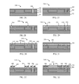
- FIG. 22 depicts the wafer of FIG. 20 with an insulating material deposited within the trenches and along the upper surface of the third cap layer portion, and a contact opening etched through the insulating material to expose a contact portion of the cap layer;
- FIGS. 8 and 9 further show trenches 230 and 232 which may be etched after CMP of the lower cap layer portion 228 .
- the trench 230 extends from the upper surface of the lower cap layer portion 228 to the upper surface of the oxide layer 222 to define the lower middle contact portion 226 .
- the trench 232 includes a trench portion 234 that defines a lower out-of-plane electrode portion 236 , a trench portion 238 that defines a connector 240 , and a trench portion 242 that defines a lower contact portion 244 for the lower out-of-plane electrode portion 236 .
Landscapes
- Engineering & Computer Science (AREA)
- Manufacturing & Machinery (AREA)
- Microelectronics & Electronic Packaging (AREA)
- Chemical & Material Sciences (AREA)
- Analytical Chemistry (AREA)
- Computer Hardware Design (AREA)
- Pressure Sensors (AREA)
- Micromachines (AREA)
Priority Applications (2)
| Application Number | Priority Date | Filing Date | Title |
|---|---|---|---|
| US14/201,453 US9469522B2 (en) | 2013-03-15 | 2014-03-07 | Epi-poly etch stop for out of plane spacer defined electrode |
| US15/291,374 US10173887B2 (en) | 2013-03-15 | 2016-10-12 | Epi-poly etch stop for out of plane spacer defined electrode |
Applications Claiming Priority (2)
| Application Number | Priority Date | Filing Date | Title |
|---|---|---|---|
| US201361787376P | 2013-03-15 | 2013-03-15 | |
| US14/201,453 US9469522B2 (en) | 2013-03-15 | 2014-03-07 | Epi-poly etch stop for out of plane spacer defined electrode |
Related Child Applications (1)
| Application Number | Title | Priority Date | Filing Date |
|---|---|---|---|
| US15/291,374 Division US10173887B2 (en) | 2013-03-15 | 2016-10-12 | Epi-poly etch stop for out of plane spacer defined electrode |
Publications (2)
| Publication Number | Publication Date |
|---|---|
| US20160137485A1 US20160137485A1 (en) | 2016-05-19 |
| US9469522B2 true US9469522B2 (en) | 2016-10-18 |
Family
ID=51580697
Family Applications (2)
| Application Number | Title | Priority Date | Filing Date |
|---|---|---|---|
| US14/201,453 Active 2035-02-03 US9469522B2 (en) | 2013-03-15 | 2014-03-07 | Epi-poly etch stop for out of plane spacer defined electrode |
| US15/291,374 Active US10173887B2 (en) | 2013-03-15 | 2016-10-12 | Epi-poly etch stop for out of plane spacer defined electrode |
Family Applications After (1)
| Application Number | Title | Priority Date | Filing Date |
|---|---|---|---|
| US15/291,374 Active US10173887B2 (en) | 2013-03-15 | 2016-10-12 | Epi-poly etch stop for out of plane spacer defined electrode |
Country Status (4)
| Country | Link |
|---|---|
| US (2) | US9469522B2 (zh) |
| EP (1) | EP2973665B1 (zh) |
| TW (1) | TWI652728B (zh) |
| WO (1) | WO2014150091A1 (zh) |
Families Citing this family (4)
| Publication number | Priority date | Publication date | Assignee | Title |
|---|---|---|---|---|
| JP5688690B2 (ja) * | 2013-01-11 | 2015-03-25 | 横河電機株式会社 | 振動式トランスデューサおよび振動式トランスデューサの製造方法 |
| FI20185058A1 (en) * | 2018-01-22 | 2019-07-23 | Tikitin Oy | Packaged microelectronic component and method for its manufacture |
| DE102020200334A1 (de) * | 2020-01-14 | 2021-07-15 | Robert Bosch Gesellschaft mit beschränkter Haftung | Mikromechanisches Bauteil für eine Sensor- oder Mikrofonvorrichtung |
| US11383973B2 (en) | 2020-01-22 | 2022-07-12 | Nxp Usa, Inc. | Sensor device and method of fabrication |
Citations (15)
| Publication number | Priority date | Publication date | Assignee | Title |
|---|---|---|---|---|
| US6158280A (en) | 1997-12-22 | 2000-12-12 | Kabushiki Kaisha Toyota Chuo Kenkyusho | Detector for detecting angular velocities about perpendicular axes |
| US20010038148A1 (en) | 2000-04-28 | 2001-11-08 | Ubaldo Mastromatteo | Structure for electrically connecting a first body of semiconductor material overlaid by a second body of semiconductor material, composite structure using the electric connection structure, and manufacturing process thereof |
| US20030214373A1 (en) | 2002-05-17 | 2003-11-20 | Andricacos Panayotis Constantinou | Micro-electro-mechanical RF switch |
| US6664126B1 (en) | 1999-09-03 | 2003-12-16 | University Of Maryland, College Park | Process for fabrication of 3-dimensional micromechanisms |
| US6913941B2 (en) | 2002-09-09 | 2005-07-05 | Freescale Semiconductor, Inc. | SOI polysilicon trench refill perimeter oxide anchor scheme |
| US7056757B2 (en) | 2003-11-25 | 2006-06-06 | Georgia Tech Research Corporation | Methods of forming oxide masks with submicron openings and microstructures formed thereby |
| US20060148133A1 (en) | 2005-01-03 | 2006-07-06 | Analog Devices, Inc. | Method of forming a MEMS device |
| US20100032775A1 (en) | 2008-07-08 | 2010-02-11 | Morris Iii Arthur S | Thin-film lid mems devices and methods |
| US20100155861A1 (en) | 2008-12-19 | 2010-06-24 | Freescale Semiconductor, Inc. | Microelectromechanical device with isolated microstructures and method of producing same |
| US20100240163A1 (en) * | 2009-03-19 | 2010-09-23 | Robert Bosch Gmbh | Substrate with multiple encapsulated pressures |
| US7825484B2 (en) | 2005-04-25 | 2010-11-02 | Analog Devices, Inc. | Micromachined microphone and multisensor and method for producing same |
| US20100295138A1 (en) | 2009-05-20 | 2010-11-25 | Baolab Microsystems Sl | Methods and systems for fabrication of mems cmos devices |
| US20110121412A1 (en) | 2007-03-09 | 2011-05-26 | Silicon Laboratories Inc. | Planar microshells for vacuum encapsulated devices and damascene method of manufacture |
| US20110127622A1 (en) | 2008-07-30 | 2011-06-02 | Robert Bosch Gmbh | Method for Capping a MEMS Wafer and MEMS Wafer |
| US20110221013A1 (en) * | 2003-06-04 | 2011-09-15 | Aaron Partridge | Microelectromechanical device including an encapsulation layer of which a portion is removed to expose a substantially planar surface having a portion that is disposed outside and above a chamber and including a field region on which integrated circuits are formed, and methods for fabricating same |
Family Cites Families (3)
| Publication number | Priority date | Publication date | Assignee | Title |
|---|---|---|---|---|
| US8021947B2 (en) | 2009-12-09 | 2011-09-20 | Semiconductor Components Industries, Llc | Method of forming an insulated gate field effect transistor device having a shield electrode structure |
| DE102011004922B4 (de) | 2011-03-01 | 2016-12-15 | Globalfoundries Dresden Module One Llc & Co. Kg | Verfahren zur Herstellung von Transistoren mit Metallgatestapeln mit erhöhter Integrität |
| US8673756B2 (en) | 2011-04-14 | 2014-03-18 | Robert Bosch Gmbh | Out-of-plane spacer defined electrode |
-
2014
- 2014-03-07 US US14/201,453 patent/US9469522B2/en active Active
- 2014-03-08 WO PCT/US2014/022186 patent/WO2014150091A1/en active Application Filing
- 2014-03-08 EP EP14770043.9A patent/EP2973665B1/en active Active
- 2014-03-12 TW TW103108629A patent/TWI652728B/zh active
-
2016
- 2016-10-12 US US15/291,374 patent/US10173887B2/en active Active
Patent Citations (15)
| Publication number | Priority date | Publication date | Assignee | Title |
|---|---|---|---|---|
| US6158280A (en) | 1997-12-22 | 2000-12-12 | Kabushiki Kaisha Toyota Chuo Kenkyusho | Detector for detecting angular velocities about perpendicular axes |
| US6664126B1 (en) | 1999-09-03 | 2003-12-16 | University Of Maryland, College Park | Process for fabrication of 3-dimensional micromechanisms |
| US20010038148A1 (en) | 2000-04-28 | 2001-11-08 | Ubaldo Mastromatteo | Structure for electrically connecting a first body of semiconductor material overlaid by a second body of semiconductor material, composite structure using the electric connection structure, and manufacturing process thereof |
| US20030214373A1 (en) | 2002-05-17 | 2003-11-20 | Andricacos Panayotis Constantinou | Micro-electro-mechanical RF switch |
| US6913941B2 (en) | 2002-09-09 | 2005-07-05 | Freescale Semiconductor, Inc. | SOI polysilicon trench refill perimeter oxide anchor scheme |
| US20110221013A1 (en) * | 2003-06-04 | 2011-09-15 | Aaron Partridge | Microelectromechanical device including an encapsulation layer of which a portion is removed to expose a substantially planar surface having a portion that is disposed outside and above a chamber and including a field region on which integrated circuits are formed, and methods for fabricating same |
| US7056757B2 (en) | 2003-11-25 | 2006-06-06 | Georgia Tech Research Corporation | Methods of forming oxide masks with submicron openings and microstructures formed thereby |
| US20060148133A1 (en) | 2005-01-03 | 2006-07-06 | Analog Devices, Inc. | Method of forming a MEMS device |
| US7825484B2 (en) | 2005-04-25 | 2010-11-02 | Analog Devices, Inc. | Micromachined microphone and multisensor and method for producing same |
| US20110121412A1 (en) | 2007-03-09 | 2011-05-26 | Silicon Laboratories Inc. | Planar microshells for vacuum encapsulated devices and damascene method of manufacture |
| US20100032775A1 (en) | 2008-07-08 | 2010-02-11 | Morris Iii Arthur S | Thin-film lid mems devices and methods |
| US20110127622A1 (en) | 2008-07-30 | 2011-06-02 | Robert Bosch Gmbh | Method for Capping a MEMS Wafer and MEMS Wafer |
| US20100155861A1 (en) | 2008-12-19 | 2010-06-24 | Freescale Semiconductor, Inc. | Microelectromechanical device with isolated microstructures and method of producing same |
| US20100240163A1 (en) * | 2009-03-19 | 2010-09-23 | Robert Bosch Gmbh | Substrate with multiple encapsulated pressures |
| US20100295138A1 (en) | 2009-05-20 | 2010-11-25 | Baolab Microsystems Sl | Methods and systems for fabrication of mems cmos devices |
Non-Patent Citations (8)
| Title |
|---|
| Candler et al., "Long-Term and Accelerated Life Testing of a Novel Single-Wafer Vacuum Encapsulation for MEMS Resonators," Journal of Microelectromechanical Systems, Dec. 2006, pp. 1446-1456, vol. 15, No. 6, IEEE, USA (11 pages). |
| Chen et al., "An Integrated Solution for Wafer-Level Packaging and Electrostatic Actuation of Out-of-Plane Devices," Micro Electro Mechanical Systems,MEMS 2009, IEEE 22nd International Conference, pp. 1071-1074, USA (4 pages). |
| Chen, "Abstract-Electrode Integrated Wafer-Level Packaging for Out-of-Plane MEMS Devices," International Microlectronics and Packaging Society, http://www.imaps.org/abstracts/system/new/abstract-preview.asp . . . published at least as early as Apr. 1, 2011 (1 pages). |
| Hyldgård et al., "Fish & Chips: Single Chip Silicon MEMS CTDL Salinity, Temperature, Pressure and Light Sensor for Use in Fisheries Research," Paper-Micro Electro Mechanical Systems, 2005. MEMS 2005. 18th IEEE International Conference (4 pages). |
| International Search Report and Written Opinion corresponding to PCT Application No. PCT/US2014/022186, mailed Jun. 27, 2014 (13 pages). |
| Park et al., "Ultraminiature encapsulated accelerometers as a fully implantable sensor for implantable hearing aids," Biomed Microdevices, 2007, Springer Science, Korea (11 pages). |
| Website page, "Encapsulation for RF MEMS," Micromachine Stanford University, http://www.micromachine.stanford.edu/~kuanlinc/Professional/Encapsulation . . . published at least as early as Apr. 1, 2011 (4 pages). |
| Website page, "Encapsulation for RF MEMS," Micromachine Stanford University, http://www.micromachine.stanford.edu/˜kuanlinc/Professional/Encapsulation . . . published at least as early as Apr. 1, 2011 (4 pages). |
Also Published As
| Publication number | Publication date |
|---|---|
| TW201447992A (zh) | 2014-12-16 |
| TWI652728B (zh) | 2019-03-01 |
| EP2973665A1 (en) | 2016-01-20 |
| US20160137485A1 (en) | 2016-05-19 |
| WO2014150091A1 (en) | 2014-09-25 |
| EP2973665B1 (en) | 2019-11-06 |
| US20170297896A1 (en) | 2017-10-19 |
| EP2973665A4 (en) | 2016-11-16 |
| US10173887B2 (en) | 2019-01-08 |
Similar Documents
| Publication | Publication Date | Title |
|---|---|---|
| US9242850B2 (en) | Out-of-plane spacer defined electrode | |
| US9908771B2 (en) | Inertial and pressure sensors on single chip | |
| US9194882B2 (en) | Inertial and pressure sensors on single chip | |
| US10173887B2 (en) | Epi-poly etch stop for out of plane spacer defined electrode | |
| JP2011220885A (ja) | 力学量検出装置およびその製造方法 | |
| US7479402B2 (en) | Comb structure fabrication methods and systems | |
| US11402288B2 (en) | Membrane-based sensor having a plurality of spacers extending from a cap layer | |
| WO2016044932A1 (en) | Fabrication method for 3d inertial sensor | |
| TWI632358B (zh) | 電容式壓力感測器及方法 | |
| US8430255B2 (en) | Method of accurately spacing Z-axis electrode |
Legal Events
| Date | Code | Title | Description |
|---|---|---|---|
| AS | Assignment |
Owner name: ROBERT BOSCH GMBH, GERMANY Free format text: ASSIGNMENT OF ASSIGNORS INTEREST;ASSIGNORS:GRAHAM, ANDREW;YAMA, GARY;O'BRIEN, GARY;SIGNING DATES FROM 20150608 TO 20150924;REEL/FRAME:036948/0648 |
|
| STCF | Information on status: patent grant |
Free format text: PATENTED CASE |
|
| MAFP | Maintenance fee payment |
Free format text: PAYMENT OF MAINTENANCE FEE, 4TH YEAR, LARGE ENTITY (ORIGINAL EVENT CODE: M1551); ENTITY STATUS OF PATENT OWNER: LARGE ENTITY Year of fee payment: 4 |
|
| MAFP | Maintenance fee payment |
Free format text: PAYMENT OF MAINTENANCE FEE, 8TH YEAR, LARGE ENTITY (ORIGINAL EVENT CODE: M1552); ENTITY STATUS OF PATENT OWNER: LARGE ENTITY Year of fee payment: 8 |