US9467132B2 - Self-powered comparator - Google Patents
Self-powered comparator Download PDFInfo
- Publication number
- US9467132B2 US9467132B2 US13/711,298 US201213711298A US9467132B2 US 9467132 B2 US9467132 B2 US 9467132B2 US 201213711298 A US201213711298 A US 201213711298A US 9467132 B2 US9467132 B2 US 9467132B2
- Authority
- US
- United States
- Prior art keywords
- voltage
- comparator
- source
- stage
- transistor
- Prior art date
- Legal status (The legal status is an assumption and is not a legal conclusion. Google has not performed a legal analysis and makes no representation as to the accuracy of the status listed.)
- Active
Links
- 238000004146 energy storage Methods 0.000 claims abstract description 50
- 239000003990 capacitor Substances 0.000 claims abstract description 9
- 238000000034 method Methods 0.000 claims description 10
- 238000003306 harvesting Methods 0.000 abstract description 8
- 238000004088 simulation Methods 0.000 description 8
- 238000005516 engineering process Methods 0.000 description 2
- 238000012986 modification Methods 0.000 description 1
- 230000004048 modification Effects 0.000 description 1
Images


Classifications
-
- H—ELECTRICITY
- H03—ELECTRONIC CIRCUITRY
- H03K—PULSE TECHNIQUE
- H03K5/00—Manipulating of pulses not covered by one of the other main groups of this subclass
- H03K5/22—Circuits having more than one input and one output for comparing pulses or pulse trains with each other according to input signal characteristics, e.g. slope, integral
-
- H—ELECTRICITY
- H03—ELECTRONIC CIRCUITRY
- H03F—AMPLIFIERS
- H03F1/00—Details of amplifiers with only discharge tubes, only semiconductor devices or only unspecified devices as amplifying elements
- H03F1/02—Modifications of amplifiers to raise the efficiency, e.g. gliding Class A stages, use of an auxiliary oscillation
- H03F1/0205—Modifications of amplifiers to raise the efficiency, e.g. gliding Class A stages, use of an auxiliary oscillation in transistor amplifiers
- H03F1/0211—Modifications of amplifiers to raise the efficiency, e.g. gliding Class A stages, use of an auxiliary oscillation in transistor amplifiers with control of the supply voltage or current
- H03F1/0216—Continuous control
- H03F1/0222—Continuous control by using a signal derived from the input signal
-
- H—ELECTRICITY
- H03—ELECTRONIC CIRCUITRY
- H03F—AMPLIFIERS
- H03F1/00—Details of amplifiers with only discharge tubes, only semiconductor devices or only unspecified devices as amplifying elements
- H03F1/02—Modifications of amplifiers to raise the efficiency, e.g. gliding Class A stages, use of an auxiliary oscillation
- H03F1/0205—Modifications of amplifiers to raise the efficiency, e.g. gliding Class A stages, use of an auxiliary oscillation in transistor amplifiers
- H03F1/0211—Modifications of amplifiers to raise the efficiency, e.g. gliding Class A stages, use of an auxiliary oscillation in transistor amplifiers with control of the supply voltage or current
- H03F1/0216—Continuous control
- H03F1/0233—Continuous control by using a signal derived from the output signal, e.g. bootstrapping the voltage supply
-
- H—ELECTRICITY
- H03—ELECTRONIC CIRCUITRY
- H03F—AMPLIFIERS
- H03F1/00—Details of amplifiers with only discharge tubes, only semiconductor devices or only unspecified devices as amplifying elements
- H03F1/02—Modifications of amplifiers to raise the efficiency, e.g. gliding Class A stages, use of an auxiliary oscillation
- H03F1/0205—Modifications of amplifiers to raise the efficiency, e.g. gliding Class A stages, use of an auxiliary oscillation in transistor amplifiers
- H03F1/0261—Modifications of amplifiers to raise the efficiency, e.g. gliding Class A stages, use of an auxiliary oscillation in transistor amplifiers with control of the polarisation voltage or current, e.g. gliding Class A
- H03F1/0266—Modifications of amplifiers to raise the efficiency, e.g. gliding Class A stages, use of an auxiliary oscillation in transistor amplifiers with control of the polarisation voltage or current, e.g. gliding Class A by using a signal derived from the input signal
-
- H—ELECTRICITY
- H03—ELECTRONIC CIRCUITRY
- H03F—AMPLIFIERS
- H03F3/00—Amplifiers with only discharge tubes or only semiconductor devices as amplifying elements
- H03F3/45—Differential amplifiers
- H03F3/45071—Differential amplifiers with semiconductor devices only
- H03F3/45076—Differential amplifiers with semiconductor devices only characterised by the way of implementation of the active amplifying circuit in the differential amplifier
- H03F3/45179—Differential amplifiers with semiconductor devices only characterised by the way of implementation of the active amplifying circuit in the differential amplifier using MOSFET transistors as the active amplifying circuit
- H03F3/45183—Long tailed pairs
-
- H—ELECTRICITY
- H03—ELECTRONIC CIRCUITRY
- H03F—AMPLIFIERS
- H03F2200/00—Indexing scheme relating to amplifiers
- H03F2200/375—Circuitry to compensate the offset being present in an amplifier
-
- H—ELECTRICITY
- H03—ELECTRONIC CIRCUITRY
- H03F—AMPLIFIERS
- H03F2200/00—Indexing scheme relating to amplifiers
- H03F2200/411—Indexing scheme relating to amplifiers the output amplifying stage of an amplifier comprising two power stages
-
- H—ELECTRICITY
- H03—ELECTRONIC CIRCUITRY
- H03F—AMPLIFIERS
- H03F2203/00—Indexing scheme relating to amplifiers with only discharge tubes or only semiconductor devices as amplifying elements covered by H03F3/00
- H03F2203/45—Indexing scheme relating to differential amplifiers
- H03F2203/45644—Indexing scheme relating to differential amplifiers the LC comprising a cross coupling circuit, e.g. comprising two cross-coupled transistors
-
- H—ELECTRICITY
- H03—ELECTRONIC CIRCUITRY
- H03K—PULSE TECHNIQUE
- H03K17/00—Electronic switching or gating, i.e. not by contact-making and –breaking
- H03K17/30—Modifications for providing a predetermined threshold before switching
- H03K2017/307—Modifications for providing a predetermined threshold before switching circuits simulating a diode, e.g. threshold zero
Definitions
- Existing active diodes used in energy harvester systems often have a comparator in an active rectifier that is powered either by an external power supply or by an energy storage element used to store the harvested energy.
- the energy storage element can be, for example, a battery or a capacitor.
- the comparator often consumes power from the energy storage element even when the system is not harvesting any energy from the input (energy harvester). By consuming power from the energy storage element when the system is not harvesting energy, the energy storage element can be unnecessarily drained and potentially not sufficiently charged when needed. In order for the comparator to draw power from the energy storage element, the energy storage element needs to have sufficient charge to power the comparator.
- the interval between two consecutive charging cycles should not be long enough for the comparator to drain the energy storage element to a point that the energy storage element no longer has sufficient energy to power the comparator, in order for the system to function properly.
- Embodiments of the invention relate to an input-powered comparator.
- Embodiments of the invention also pertain to an active diode that includes an input-powered comparator and a switch.
- the input-powered comparator only consumes power when an input source provides sufficiently high voltage.
- Embodiments of the active diode can be used in an energy harvesting system.
- the comparator can be powered by the input and the system can be configured such that the comparator only consumes power when the input is ready to provide power to the load or energy storage element.
- the comparator does not draw any power from the energy storage element (e.g., battery or capacitor) of the system.
- the input can be used as a power supply for the comparator, which can reduce, or eliminate, the stand-by power used when the input is zero, too low in power to be harvested, or meets other criteria.
- Embodiments of the subject energy harvester system can eliminate the need for pre-charging, have greater efficiency, and allow for indefinitely long intervals between charging cycles.
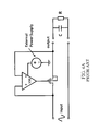
- FIG. 1 shows a self-powered voltage comparator in accordance with an embodiment of the subject invention.
- FIG. 2A shows a schematic of an embodiment of the input-powered voltage comparator of FIG. 1 .
- FIG. 2B shows a schematic of a specific embodiment of the input-powered voltage comparator of FIG. 1 with reduced offset.
- FIG. 2C shows a schematic of an embodiment of the input-powered voltage comparator of FIG. 1 .
- FIG. 4A shows a schematic of a commonly used external-powered active diode circuit.
- FIG. 4B shows a schematic of a specific embodiment of an output-powered active diode circuit.
- FIG. 5A shows a schematic of an input-powered active diode circuit in accordance with an embodiment of the subject invention.
- FIG. 5B shows simulation results for the circuitry of FIG. 5A .
- Embodiments of the invention relate to an input-powered comparator.
- Embodiments of the invention also pertain to an active diode that includes an input-powered comparator and a switch.
- the input-powered comparator only consumes power when an input source provides sufficiently high voltage.
- Embodiments of the active diode can be used in an energy harvesting system.
- the comparator can be powered by the input and the system can be configured such that the comparator only consumes power when the input is ready to provide power to the load or energy storage element.
- the comparator does not draw any power from the energy storage element (e.g., battery or capacitor) of the system.
- the input can be used as a power supply for the comparator, which can reduce, or eliminate, the stand-by power used when the input is zero, too low in power to be harvested, or meets other criteria.
- Embodiments of the subject energy harvester system can eliminate the need for pre-charging, have greater efficiency, and allow for indefinitely long intervals between charging cycles.
- FIG. 1 shows a self-powered voltage comparator in accordance with an embodiment of the subject invention.
- the comparator has two input pins (V+, V ⁇ ), one power supply pin (VDD), and one output pin (Vout). There need not be a separate power supply for the comparator as the comparator is powered, if needed, by the input.
- the power supply pin is connected with one of the input pins (V+) such that the comparator is supplied power via the V+ input pin.
- Vout When the voltage at V+ is greater than at V ⁇ , Vout is low, e.g., a zero voltage. When the voltage of V+ is less than the voltage at V ⁇ , Vout is high.
- this pattern for Vout can be reversed such that Vout is high when V+ is greater than V ⁇ and Vout is low when V+ is less than V ⁇ .
- An energy harvester, or other input can be connected to V+ such that the energy harvester can turn on the comparator and power the comparator.
- the energy storage element of the energy harvester system is connected to V ⁇ , such as a capacitor of an energy storage element.
- FIGS. 2A-2B Two schematics of the comparator of FIG. 1 are shown in FIGS. 2A-2B , where both of the schematics are functional circuits verified by simulation.
- FIG. 2B shows a schematic of a comparator with less offset than the comparator represented by the schematic of FIG. 2A .
- the schematic of FIG. 2B can be considered to have two stages.
- the first stage includes a differential transistor pair (M 3 , M 4 ) and a latch (M 1 , M 2 ).
- the second stage (M 6 , M 8 ) inverts the input to gate of M 6 with M 7 added to reduce the comparator offset.
- the first stage's power supply (VDD) connects to input (V+).
- the second stage's power supply (VDD) connects to the input (V+).
- Bias voltage (M 5 gate voltage and M 8 gate voltage) for both stages is provided by input (V+).
- V ⁇ can be connected to a capacitor of the energy storage element. The voltage can be brought to VDD and M 5 gate and M 8 gate via separate electrical connectors connected to the input and/or V+.
- the second stage (M 6 , M 8 ) and/or M 7 can be removed and the input to the gate of M 6 can be the output of the comparator.
- Such an embodiment can have an inverted Vout profile and may not have the same range of output voltages, and, therefore, may not be as desirable, as the second stage (M 6 , M 8 ) also rectifies the output voltage and increases the voltage range of output voltages.
- the circuit can be built on CMOS technology. In an embodiment, all of the transistors are CMOS transistors. In alternative embodiments, other types of transistors can be utilized to implement the comparator.
- a specific CMOS circuit was simulated with AMI 0.6um process model. The simulation indicates the circuit functions correctly with input voltage varying from 400 mV to 2.0V, as shown in FIG. 3A and FIG. 3B .
- the circuit uses technology scalable in other processes. For example, with scaled transistors' width and length, the circuit works in simulation with a CMOS 0.35um and 0.13um process model. The circuit is also fabricated as a chip using Onsemi 0.5um process and the chip works as the simulation result.
- FIG. 4A and FIG. 4B show commonly used active diodes.
- the comparators are either powered by, for example, an external power supply or an output storage capacitor.
- FIG. 5A embodiments of the invention can use the input as the power supply for the comparator.
- the circuitry for an input-powered active diode is shown in FIG. 5A .
- the comparator and the CMOS transistor, taken together, can be considered an active diode.
- Simulation results for the circuitry of FIG. 5A are shown in FIG. 5B .
- the energy harvester can connect to the input at the left, which connects to the V+ pin of the comparator.
- the energy harvester also connects to the source of the CMOS transistor, which functions as a switch to allow power to be delivered from the energy harvester to the energy storage element.
- the switch can be, for example, a BJT transistor, a JFET transistor, or an analog switch.
- the drain of the CMOS transistor is connected to the energy storage element and to the V ⁇ pin of the comparator.
- the energy storage element is represented on the right of the FIG. 5A as a capacitor, C, in parallel with resistor, R.
- the output, Vout, of the comparator is connected to the gate of the CMOS transistor (switch) and turns the CMOS transistor on when Vout is low, allowing power to flow from the energy harvester to the energy storage element.
- Other transistors can be used instead of the CMOS transistor.
- a CMOS transistor, or other transistor type can be turned on when the voltage applied to the gate is high.
- a transistor that turns on with a high voltage applied to the gate can be used and an inverter can be introduced between the output of the comparator, Vout, and the gate of the transistor.
- Vout when the energy harvester has a voltage (V+) above the voltage of the energy storage element (V ⁇ ), Vout is low, thus turning on the CMOS transistor (switch) and allowing power to flow from the energy harvester to the energy storage element.
- the comparator when the energy harvester voltage is higher than the energy storage element voltage, the comparator is powered by the energy harvester, and when the energy harvester voltage is lower than the energy storage element voltage, the comparator does not use any power.
- the first stage of the comparator is powered by the energy harvester.
Landscapes
- Engineering & Computer Science (AREA)
- Power Engineering (AREA)
- Physics & Mathematics (AREA)
- Nonlinear Science (AREA)
- Manipulation Of Pulses (AREA)
- Measurement Of Current Or Voltage (AREA)
Abstract
Description
Claims (20)
Priority Applications (1)
| Application Number | Priority Date | Filing Date | Title |
|---|---|---|---|
| US13/711,298 US9467132B2 (en) | 2009-11-09 | 2012-12-11 | Self-powered comparator |
Applications Claiming Priority (3)
| Application Number | Priority Date | Filing Date | Title |
|---|---|---|---|
| US25944809P | 2009-11-09 | 2009-11-09 | |
| US12/942,768 US8354871B2 (en) | 2009-11-09 | 2010-11-09 | Self-powered comparator |
| US13/711,298 US9467132B2 (en) | 2009-11-09 | 2012-12-11 | Self-powered comparator |
Related Parent Applications (1)
| Application Number | Title | Priority Date | Filing Date |
|---|---|---|---|
| US12/942,768 Division US8354871B2 (en) | 2009-11-09 | 2010-11-09 | Self-powered comparator |
Publications (2)
| Publication Number | Publication Date |
|---|---|
| US20130106465A1 US20130106465A1 (en) | 2013-05-02 |
| US9467132B2 true US9467132B2 (en) | 2016-10-11 |
Family
ID=43973699
Family Applications (2)
| Application Number | Title | Priority Date | Filing Date |
|---|---|---|---|
| US12/942,768 Active 2031-03-16 US8354871B2 (en) | 2009-11-09 | 2010-11-09 | Self-powered comparator |
| US13/711,298 Active US9467132B2 (en) | 2009-11-09 | 2012-12-11 | Self-powered comparator |
Family Applications Before (1)
| Application Number | Title | Priority Date | Filing Date |
|---|---|---|---|
| US12/942,768 Active 2031-03-16 US8354871B2 (en) | 2009-11-09 | 2010-11-09 | Self-powered comparator |
Country Status (1)
| Country | Link |
|---|---|
| US (2) | US8354871B2 (en) |
Families Citing this family (6)
| Publication number | Priority date | Publication date | Assignee | Title |
|---|---|---|---|---|
| US8354871B2 (en) * | 2009-11-09 | 2013-01-15 | University Of Florida Research Foundation, Inc. | Self-powered comparator |
| WO2014091088A1 (en) * | 2012-12-11 | 2014-06-19 | Commissariat A L'energie Atomique Et Aux Energies Alternatives | Circuit for comparison of a voltage with a threshold and conversion of electrical energy |
| US9706269B2 (en) * | 2015-07-24 | 2017-07-11 | Hong Kong Applied Science and Technology Research Institute Company, Limited | Self-powered and battery-assisted CMOS wireless bio-sensing IC platform |
| US10615712B2 (en) | 2016-11-11 | 2020-04-07 | Qualcomm Incorporated | Self-powered clock input buffer |
| US10425073B1 (en) * | 2018-03-23 | 2019-09-24 | Dialog Semiconductor B.V. | Digital active diode circuit |
| TWI733358B (en) * | 2020-03-06 | 2021-07-11 | 國立陽明交通大學 | Ideal diode |
Citations (12)
| Publication number | Priority date | Publication date | Assignee | Title |
|---|---|---|---|---|
| US4598215A (en) * | 1983-11-03 | 1986-07-01 | Motorola, Inc. | Wide common mode range analog CMOS voltage comparator |
| US4611130A (en) * | 1984-02-13 | 1986-09-09 | At&T Bell Laboratories | Floating input comparator with precharging of input parasitic capacitors |
| US5012450A (en) * | 1987-08-18 | 1991-04-30 | Siemens Aktiengesellschaft | Read amplifier for static memories in CMOS technology |
| US5099302A (en) | 1988-09-14 | 1992-03-24 | Sgs-Thomson Microelectronics, S.A. | Integrable active diode |
| WO1997024795A1 (en) | 1995-12-29 | 1997-07-10 | Em Microelectronic-Marin S.A. | Active rectifier having minimal energy losses |
| US6781804B1 (en) | 1997-06-17 | 2004-08-24 | Sgs-Thomson Microelectronics S.A. | Protection of the logic well of a component including an integrated MOS power transistor |
| WO2005064793A1 (en) | 2003-12-23 | 2005-07-14 | Honeywell International Inc. | Single event transient filter for comparator |
| US7199636B2 (en) | 2004-03-31 | 2007-04-03 | Matsushita Electric Industrial Co., Ltd. | Active diode |
| WO2007055265A1 (en) | 2005-11-11 | 2007-05-18 | Matsushita Electric Industrial Co., Ltd. | Power source device |
| US20070141874A1 (en) | 2005-02-17 | 2007-06-21 | General Electric Company | Power control system and method |
| US7429805B2 (en) | 2002-03-07 | 2008-09-30 | Microstrain, Inc. | Energy harvesting for wireless sensor operation and data transmission |
| US8354871B2 (en) * | 2009-11-09 | 2013-01-15 | University Of Florida Research Foundation, Inc. | Self-powered comparator |
Family Cites Families (5)
| Publication number | Priority date | Publication date | Assignee | Title |
|---|---|---|---|---|
| US6469564B1 (en) * | 1998-04-14 | 2002-10-22 | Minebea Co., Ltd. | Circuit simulating a diode |
| US6060943A (en) * | 1998-04-14 | 2000-05-09 | Nmb (Usa) Inc. | Circuit simulating a diode |
| US6501320B1 (en) * | 2000-07-25 | 2002-12-31 | Exar Corporation | Self-powered, maximum-conductive, low turn-on voltage CMOS rectifier |
| DE60217478D1 (en) * | 2001-03-28 | 2007-02-22 | Koninkl Philips Electronics Nv | Sychrongleichrichter |
| TWI222754B (en) * | 2002-10-23 | 2004-10-21 | Quanta Comp Inc | One-way conduction apparatus |
-
2010
- 2010-11-09 US US12/942,768 patent/US8354871B2/en active Active
-
2012
- 2012-12-11 US US13/711,298 patent/US9467132B2/en active Active
Patent Citations (13)
| Publication number | Priority date | Publication date | Assignee | Title |
|---|---|---|---|---|
| US4598215A (en) * | 1983-11-03 | 1986-07-01 | Motorola, Inc. | Wide common mode range analog CMOS voltage comparator |
| US4611130A (en) * | 1984-02-13 | 1986-09-09 | At&T Bell Laboratories | Floating input comparator with precharging of input parasitic capacitors |
| US5012450A (en) * | 1987-08-18 | 1991-04-30 | Siemens Aktiengesellschaft | Read amplifier for static memories in CMOS technology |
| US5099302A (en) | 1988-09-14 | 1992-03-24 | Sgs-Thomson Microelectronics, S.A. | Integrable active diode |
| WO1997024795A1 (en) | 1995-12-29 | 1997-07-10 | Em Microelectronic-Marin S.A. | Active rectifier having minimal energy losses |
| US6781804B1 (en) | 1997-06-17 | 2004-08-24 | Sgs-Thomson Microelectronics S.A. | Protection of the logic well of a component including an integrated MOS power transistor |
| US7429805B2 (en) | 2002-03-07 | 2008-09-30 | Microstrain, Inc. | Energy harvesting for wireless sensor operation and data transmission |
| WO2005064793A1 (en) | 2003-12-23 | 2005-07-14 | Honeywell International Inc. | Single event transient filter for comparator |
| US7199636B2 (en) | 2004-03-31 | 2007-04-03 | Matsushita Electric Industrial Co., Ltd. | Active diode |
| US20070141874A1 (en) | 2005-02-17 | 2007-06-21 | General Electric Company | Power control system and method |
| US7331803B2 (en) | 2005-02-17 | 2008-02-19 | General Electric Company | Power control system and method |
| WO2007055265A1 (en) | 2005-11-11 | 2007-05-18 | Matsushita Electric Industrial Co., Ltd. | Power source device |
| US8354871B2 (en) * | 2009-11-09 | 2013-01-15 | University Of Florida Research Foundation, Inc. | Self-powered comparator |
Non-Patent Citations (8)
| Title |
|---|
| Cheng, S., "Modeling of Magnetic Vibrational Energy Harvesters Using Equivalent Circuit Representations," Journal of Micromechanics and Microengineering, Nov. 2007, pp. 2328-2335, vol. 17, No. 11. |
| Liu, Y., et al., "Active Piezoelectric Energy Harvesting: General Principle and Experimental Demonstration," Journal of Intelligent Material Systems and Structures, Mar. 2009, pp. 575-585, vol. 20, No. 5. |
| Maurath, D., et al., "Highly Efficient Integrated Rectifier and Voltage Boosting Circuits for Energy Harvesting Applications," Advanced in Radio Science, 2008, pp. 219-225, vol. 6. |
| Notice of Allowance dated Oct. 30, 2012 in U.S. Appl. No. 12/942,768. |
| Office Action dated Jun. 11, 2012 in U.S. Appl. No. 12/942,768. |
| Sze, N.-M., et al. "Integrated Single-Inductor Dual-Input Dual-Output Boost Converter for Energy Harvesting Applications," 2008 IEEE International Symposium on Circuits and Systems, May 18-21, 2008, Seattle, WA, pp. 2218-2221. |
| Texas Instruments, "Energy harvesting becomes reality with AdaptivEnergy's wireless, remote sensing solution based on TI ultra-low power technology," Texas Instruments NewsCenter, Aug. 19, 2008, http://newscenter.ti.com/Blogs/newsroom/archive/2008/08/19/energy-harvesting-becomes-reality-with-adaptivenergy-s-wireless-remote-sensing-solution-based-on-ti-ultra-low-power-technology-sc08102.aspx. |
| Vullers, R.J.M., et al., "Micropower Energy Harvesting," Solid-State Electronics, Jul. 2009, pp. 684-693, vol. 53, No. 7. |
Also Published As
| Publication number | Publication date |
|---|---|
| US8354871B2 (en) | 2013-01-15 |
| US20130106465A1 (en) | 2013-05-02 |
| US20110109347A1 (en) | 2011-05-12 |
Similar Documents
| Publication | Publication Date | Title |
|---|---|---|
| US9467132B2 (en) | Self-powered comparator | |
| US8415837B2 (en) | Switch mode voltage rectifier, RF energy conversion and wireless power supplies | |
| US20140169043A1 (en) | Bias voltage generating circuit and switching power supply thereof | |
| US20150357864A1 (en) | Power source switching apparatus and methods for dual-powered electronic devices | |
| US20110134674A1 (en) | Active rectifier and method for energy harvesting power management circuit | |
| CN102047520B (en) | Hot swap controller with zero loaded charge pump | |
| US20130155742A1 (en) | Micro-power rectifier and method thereof | |
| US9679469B2 (en) | Remote control circuit | |
| CN103970176B (en) | A kind of low-dropout linear voltage-regulating circuit and application system thereof | |
| Zulkifli et al. | Optimization of RF-DC converter in micro energy harvester using voltage boosting network and bulk modulation technique for biomedical devices | |
| KR102615295B1 (en) | Load connection device for energy havester | |
| US9025290B2 (en) | Protective circuit for loads | |
| CN105186598A (en) | USB insertion automatic identification and power supply system and chip integrated with the same | |
| WO2018133484A1 (en) | Control circuit compatible with battery power supply and external power supply | |
| US10355192B2 (en) | Autonomous thermoelectric energy harvesting platform for biomedical sensors | |
| Cho et al. | An area-efficient rectifier with threshold voltage cancellation for intra-body power transfer | |
| CN109194126B (en) | Power supply switching circuit | |
| US20160181923A1 (en) | Power supply circuit and notebook computer including the same | |
| CN110429680B (en) | Power supply circuit of double chargers | |
| CN106209064B (en) | Low-power consumption dynamic threshold comparator interface circuit and rectifier, wireless sensor | |
| Potocny et al. | Self Vth-compensating CMOS on-chip rectifier for inductively powered implantable medical devices | |
| CN116349109A (en) | Charging circuit and electronic equipment | |
| CN209389712U (en) | A kind of high order side redundant circuit with diagnostic function | |
| CN109038741B (en) | Charging circuit, switch charging chip and charging current sampling circuit thereof | |
| CN219678160U (en) | Non-polar installation device of battery and mobile electronic consumer equipment |
Legal Events
| Date | Code | Title | Description |
|---|---|---|---|
| AS | Assignment |
Owner name: UNIVERSITY OF FLORIDA RESEARCH FOUNDATION, INC., F Free format text: ASSIGNMENT OF ASSIGNORS INTEREST;ASSIGNOR:RAO, YUAN;REEL/FRAME:029574/0283 Effective date: 20101119 |
|
| STCF | Information on status: patent grant |
Free format text: PATENTED CASE |
|
| MAFP | Maintenance fee payment |
Free format text: PAYMENT OF MAINTENANCE FEE, 4TH YR, SMALL ENTITY (ORIGINAL EVENT CODE: M2551); ENTITY STATUS OF PATENT OWNER: SMALL ENTITY Year of fee payment: 4 |
|
| MAFP | Maintenance fee payment |
Free format text: PAYMENT OF MAINTENANCE FEE, 8TH YR, SMALL ENTITY (ORIGINAL EVENT CODE: M2552); ENTITY STATUS OF PATENT OWNER: SMALL ENTITY Year of fee payment: 8 |