US9466628B2 - Spectral imaging device and method to calibrate the same - Google Patents
Spectral imaging device and method to calibrate the same Download PDFInfo
- Publication number
- US9466628B2 US9466628B2 US14/135,872 US201314135872A US9466628B2 US 9466628 B2 US9466628 B2 US 9466628B2 US 201314135872 A US201314135872 A US 201314135872A US 9466628 B2 US9466628 B2 US 9466628B2
- Authority
- US
- United States
- Prior art keywords
- optical filter
- electrode
- spectral
- bragg reflector
- spectral data
- Prior art date
- Legal status (The legal status is an assumption and is not a legal conclusion. Google has not performed a legal analysis and makes no representation as to the accuracy of the status listed.)
- Expired - Fee Related, expires
Links
Images


Classifications
-
- H01L27/14625—
-
- H—ELECTRICITY
- H10—SEMICONDUCTOR DEVICES; ELECTRIC SOLID-STATE DEVICES NOT OTHERWISE PROVIDED FOR
- H10F—INORGANIC SEMICONDUCTOR DEVICES SENSITIVE TO INFRARED RADIATION, LIGHT, ELECTROMAGNETIC RADIATION OF SHORTER WAVELENGTH OR CORPUSCULAR RADIATION
- H10F39/00—Integrated devices, or assemblies of multiple devices, comprising at least one element covered by group H10F30/00, e.g. radiation detectors comprising photodiode arrays
- H10F39/80—Constructional details of image sensors
- H10F39/806—Optical elements or arrangements associated with the image sensors
-
- G—PHYSICS
- G01—MEASURING; TESTING
- G01B—MEASURING LENGTH, THICKNESS OR SIMILAR LINEAR DIMENSIONS; MEASURING ANGLES; MEASURING AREAS; MEASURING IRREGULARITIES OF SURFACES OR CONTOURS
- G01B7/00—Measuring arrangements characterised by the use of electric or magnetic techniques
- G01B7/02—Measuring arrangements characterised by the use of electric or magnetic techniques for measuring length, width or thickness
- G01B7/06—Measuring arrangements characterised by the use of electric or magnetic techniques for measuring length, width or thickness for measuring thickness
- G01B7/08—Measuring arrangements characterised by the use of electric or magnetic techniques for measuring length, width or thickness for measuring thickness using capacitive means
-
- G—PHYSICS
- G01—MEASURING; TESTING
- G01J—MEASUREMENT OF INTENSITY, VELOCITY, SPECTRAL CONTENT, POLARISATION, PHASE OR PULSE CHARACTERISTICS OF INFRARED, VISIBLE OR ULTRAVIOLET LIGHT; COLORIMETRY; RADIATION PYROMETRY
- G01J3/00—Spectrometry; Spectrophotometry; Monochromators; Measuring colours
- G01J3/02—Details
- G01J3/0297—Constructional arrangements for removing other types of optical noise or for performing calibration
-
- G—PHYSICS
- G01—MEASURING; TESTING
- G01J—MEASUREMENT OF INTENSITY, VELOCITY, SPECTRAL CONTENT, POLARISATION, PHASE OR PULSE CHARACTERISTICS OF INFRARED, VISIBLE OR ULTRAVIOLET LIGHT; COLORIMETRY; RADIATION PYROMETRY
- G01J3/00—Spectrometry; Spectrophotometry; Monochromators; Measuring colours
- G01J3/12—Generating the spectrum; Monochromators
- G01J3/26—Generating the spectrum; Monochromators using multiple reflection, e.g. Fabry-Perot interferometer, variable interference filters
-
- G—PHYSICS
- G01—MEASURING; TESTING
- G01J—MEASUREMENT OF INTENSITY, VELOCITY, SPECTRAL CONTENT, POLARISATION, PHASE OR PULSE CHARACTERISTICS OF INFRARED, VISIBLE OR ULTRAVIOLET LIGHT; COLORIMETRY; RADIATION PYROMETRY
- G01J3/00—Spectrometry; Spectrophotometry; Monochromators; Measuring colours
- G01J3/28—Investigating the spectrum
- G01J3/2823—Imaging spectrometer
-
- G—PHYSICS
- G01—MEASURING; TESTING
- G01J—MEASUREMENT OF INTENSITY, VELOCITY, SPECTRAL CONTENT, POLARISATION, PHASE OR PULSE CHARACTERISTICS OF INFRARED, VISIBLE OR ULTRAVIOLET LIGHT; COLORIMETRY; RADIATION PYROMETRY
- G01J3/00—Spectrometry; Spectrophotometry; Monochromators; Measuring colours
- G01J3/28—Investigating the spectrum
- G01J3/30—Measuring the intensity of spectral lines directly on the spectrum itself
- G01J3/36—Investigating two or more bands of a spectrum by separate detectors
Definitions
- the field of the disclosure is related to spectral imaging.
- it is related to spectral imaging devices and techniques to calibrate spectral data of light.
- Spectral imaging is a technique to extract spectral data from an image.
- State of the art spectral imaging devices contain optical filters positioned on top of an image sensor for filtering and recording incoming light. The filter cavity of each optical filter determines the central wavelength of the spectral band of each optical filter.
- Some state of the art systems use Fabry-Perot filters which are processed directly on top of the image sensor. Due to intolerances of the fabrication process, there is a misalignment between the actual height of each optical filter cavity and the intended height. This misalignment influences the performance of the spectral imaging device. Apart from fabrication intolerances, changes in environmental conditions such as temperature, pressure or humidity also influence the performance of the spectral imaging device.
- a solid-state spectral imaging device comprising: an image sensor; a plurality of optical filters directly processed on top of the image sensor, each optical filter comprising: a first and a second mirror defining an optical filter cavity, the optical filter cavity having a fixed height; characterized in that: each optical filter further comprises a first and a second electrode having a fixed position located opposite to each other and positioned to measure the height of the filter cavity.
- the spectral imaging device further comprises electronic circuitry configured to measure a dielectric capacitance between the first and second electrodes.
- the electronic circuitry is further configured to: determine the height of the optical filter cavity using the measured dielectric capacitance; determine the central wavelength of the spectral band of the optical filter using the determined height of the optical filter cavity; and calibrate spectral data of recorded filtered light using the determined central wavelength of the spectral band information of each optical filter.
- each optical filter is a Fabry-Perot filter and the first and the second mirror are Bragg reflectors, each Bragg reflector comprising a plurality of layers, wherein a first layer of the first Bragg reflector, adjacent to the optical filter cavity, comprises the first electrode and wherein a first layer of the second Bragg reflector, adjacent to the optical filter cavity, comprises the second electrode.
- a second layer of the first Bragg reflector adjacent to the first layer comprises an electrode.
- the first layer of the first Bragg reflector further comprises another electrode and the first layer of the second Bragg reflector further comprises another electrode.
- At least one of the electrodes is fabricated from a transparent material.
- a method for calibrating spectral data of light detected by the solid-state spectral imaging device comprises: filtering light using an optical filter, the optical filter comprising a first and a second mirror defining an optical filter cavity, the optical filter cavity being filled with a solid material; recording filtered light and storing spectral data of the filtered light; determining a height of the optical filter cavity; determining the central wavelength of the spectral band of the optical filter using the determined height of the optical filter cavity; and calibrating the stored spectral data of the filtered light using the determined central wavelength of the spectral band of the optical filter.
- determining the height of the optical filter cavity comprises: performing a capacitance measurement on the optical filter, and determining the height of the optical filter cavity using the capacitance measurement information.
- the method further comprises determining a refractive index value of the solid material filling the optical cavity; and determining the central wavelength of the spectral band of the optical filter further comprises using the determined refractive index value of the solid material.
- the first and the second mirror are Bragg reflectors, each Bragg reflector comprising a plurality of layers, the method further comprising: determining a refractive index value of one or more layers of the first and/or the second mirror of the optical filter, and determining the spectral width of the optical filter using the determined refractive index value of one or more layers of the first and/or the second mirror of the optical filter.
- calibrating the stored spectral data further uses the determined spectral width of the optical filter.
- calibrating the stored spectral data comprises assigning the stored spectral data of the recorded filtered light to the determined central wavelength of the spectral band of the optical filter.
- calibrating the stored spectral data comprises: combining the stored spectral data of the recorded filtered light of one optical filer with spectral data of recorded filtered light of another optical filter and performing an interpolation to determine spectral data of light filtered by an optical filter with a different filter wavelength.
- a computer program product for calibrating spectral data of light detected by the solid-state spectral imaging device comprising: receiving spectral data of light filtered by an optical filter, the optical filter comprising a first and a second mirror defining an optical filter cavity, the optical filter cavity being filled with a solid material; receiving a dielectric capacitance value of the optical filter; determining a height of the optical filter cavity from the dielectric capacitance value, and calibrating the spectral data of light using the determined height of the optical filter cavity.
- a machine readable data storage medium is presented for storing the computer program product presented in the third aspect of the disclosure.
- FIG. 1 illustrates a spectral imaging device with an optical filter and electrodes, according to an embodiment of the disclosure.
- FIG. 2 illustrates a spectral imaging device with an optical filter and electrodes, according to an embodiment of the disclosure.
- FIG. 3 illustrates a spectral imaging device with different optical filters and electrodes, according to an embodiment of the disclosure.
- FIG. 4 illustrates a spectral imaging device with an optical filter and electrodes, according to an embodiment of the disclosure.
- FIG. 5 illustrates a spectral imaging device with an optical filter and electrodes, according to an embodiment of the disclosure.
- FIG. 6 illustrates a spectral imaging device with an optical filter and electrodes, according to an embodiment of the disclosure.
- FIG. 7 illustrates a spectral imaging device with an optical filter and electrodes, according to an embodiment of the disclosure.
- FIG. 8 illustrates a spectral imaging device with an optical filter and electrodes, according to an embodiment of the disclosure.
- FIG. 9 illustrates a spectral imaging device with an optical filter and electrodes, according to an embodiment of the disclosure.
- FIG. 10 illustrates a spectral imaging device with an optical filter and electrodes, according to an embodiment of the disclosure.
- FIG. 11 illustrates a spectral imaging device with an optical filter and electrodes embedded in oxide layers, according to an embodiment of the disclosure.
- FIG. 12 is a block diagram of a method to calibrate spectral data of recorded light, according to an embodiment of the disclosure.
- solid-state This may refer to the absence of moving parts.
- a “solid-state spectral imaging device” is a spectral imaging device in which all parts of the device have a fixed, non-movable position.
- spectral data of light This may refer to the energy quanta of the light.
- spectral data of recorded light may refer to the energy quanta of the light which are detected or recorded by a detector.
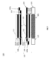
- a solid-state spectral imaging device 100 comprises: an image sensor 101 and a plurality of optical filters 102 located and processed directly on top of the image sensor 101 .
- Each optical filter 102 comprises a first and a second mirror 106 , 107 who define an optical filter cavity 113 .
- Each optical filter cavity 113 has a fixed height.
- Each optical filter further comprises a first and a second electrode 103 , 104 arranged to measure the height of the optical filter cavity 113 .
- the first and second electrodes 103 , 104 of each optical filter have a fixed position and are located opposite to each other.
- the spectral imaging device 100 further comprises electronic circuitry 105 configured to measure a dielectric capacitance between the first and second electrodes 103 , 104 .
- FIG. 1 illustrates a spectral imaging device 100 with one optical filter 102 on top of an image sensor 101 .
- the spectral imaging device 100 comprises a plurality of optical filters 102 .
- the spectral imaging device comprises 128 optical filters 102 .
- the plurality of optical filters 102 are processed directly on top of the image sensor 102 using semiconductor fabrication techniques, e.g., CMOS compatible processing steps.
- the image sensor 101 may be a conventional image sensor, e.g., a CMOS image sensor.
- Each optical filter 102 may be a Fabry-Perot filter comprising a first 106 and a second 107 mirror.
- the first 106 and the second 107 mirror may be reflective layers, e.g., metal layers.
- the plane of the first 106 and the second 107 mirror may be parallel or substantially parallel to each other.
- the plane of the first 106 and the second 107 mirror may be parallel or substantially parallel to the plane of the image sensor 101 .
- the space in between the first 106 and the second 107 mirror is defined as the optical filter cavity 113 of an optical filter 102 .
- the material filling the optical filter cavity may be a solid material, e.g., a semiconductor material or a dielectric material such as an oxide.
- Each optical filter 102 further comprises a first 103 and a second 104 electrode of which the position is fixed during manufacturing of the optical filter.
- the first 103 and second 104 electrodes cannot be moved.
- the first 103 and second 104 electrodes are positioned opposite to each other, thereby allowing a capacitance measurement between the first 103 and the second 104 electrodes to be performed.
- the first electrode 103 may be positioned at the level of the first mirror 106 .
- the second electrode 104 may be positioned at the level of the second mirror 107 .
- the second electrode 107 is positioned at the same distance and same side from the image sensor 101 .
- Each mirror of the optical filter 102 may comprise an electrode ( 103 , 104 ) at a fixed position, whereby these electrode are positioned (opposite to each other) to measure the height of the optical filter cavity 113 .
- the spectral imaging device 100 may further comprise electronic circuitry 105 electrically connected to the first 103 and second 104 electrodes of each optical filter 102 .
- the electronic circuitry 105 may be configured to measure a capacitance between the first 103 and the second 104 electrodes of each optical filter 102 .
- the electronic circuitry 105 may comprise a measurement unit configured to measure a capacitance between the first 103 and the second 104 electrodes of each optical filter 102 .
- the electronic circuitry 105 may be further configured to: determine the height of each optical filter cavity 113 using the dielectric capacitance measured between the first 103 and the second 104 electrodes, thereafter determine the central wavelength of the spectral band of each optical filter 102 using the determined height of each optical filter cavity 113 , and thereafter calibrate spectral data of recorded filtered light using the determined central wavelength of the spectral band of each optical filter 102 .
- the electronic circuitry 105 may comprise a computing unit, e.g., a micro-processor.
- Incoming light is filtered by the plurality of optical filters 102 of the spectral imaging device 100 .
- the filtered light is recorded by the image sensor 101 .
- Measured capacitances may be related to the height of the optical filter cavities, e.g., using a look-up table stored in a memory module of the electronic circuitry 105 .
- the electronic circuitry 105 may be configured to calculate the height of each optical filter cavity 113 using the measured capacitance value of each optical filer 102 .
- the central wavelength of the spectral band of each optical filter 102 is related to the height of the optical filter cavity 113 , the central wavelength of the spectral band of the optical filter 102 may be determined.
- the relation between the height of an optical filter cavity 113 and the central wavelength of the spectral band of an optical filter 102 may also be defined in a look-up table which may be stored in a memory module of the electronic circuitry 105 .
- the electronic circuitry 105 may be further configured to calibrate spectral data of recorded filtered light using the determined central wavelength of the spectral band of optical filters.
- the electronic circuitry 105 may be configured to combine spectral data of recorded filtered light of one optical filter 102 with spectral data of recorded filtered light of another optical filter and to perform an interpolation between both spectral data to determine spectral data of light at a different wavelength.
- the electronic circuitry 105 may also be configured to assign the spectral data of the recorded filtered light of an optical filter 102 to the determined central wavelength of the spectral band of the optical filter 102 .
- the electronic circuitry may be configured to link the spectral data or the energy quanta of the filtered light to that determined central wavelength of 150 nm.
- “assigning” means the aligning, linking or registering of the spectral data of recorded filtered light to the newly determined or corrected wavelength of the optical filter.
- the electronic circuitry may be configured to determine the refractive index of the material of the optical filter cavity 113 and to use this information to improve the determination of the central wavelength of the spectral band of each optical filter. Taking into account this refractive index information leads to a more accurate determination of the central wavelength of the optical filter, thereby leading to an improved calibration of spectral data.
- the electronic circuitry may be further configured to: determine the refractive index of one or more layers of the first 103 and second 104 mirror of each optical filter 102 , use this information to determine the spectral width of the optical filter; and use the information on the spectral width of the optical filter to improve calibration of spectral data. Determining the refractive index of different layers of mirrors of each optical filter may be done when the mirror are Bragg reflectors.
- FIG. 2 illustrates a spectral imaging device 100 with one optical filter 102 .
- the optical filter 102 is a Fabry-Perot filter with two reflective layers 103 , 104 .
- the optical filter 102 comprises two pairs of electrodes 115 , 116 .
- the first pair of electrodes 115 comprises a first 103 and a second 104 electrode.
- the first electrode 103 is located at the position of the first mirror 106 .
- the second electrode 104 is located at the position of the second mirror 107 .
- the second pair of electrodes 116 comprises a third 108 and a fourth 109 electrode.
- the third electrode 108 is located at the position of the first mirror 106 .
- the fourth electrode 109 is located at the position of the second mirror 107 .
- the first pair of electrodes 115 is located at one end of the first and second mirrors 106 , 107 .
- the second pair of electrodes 116 is located at an opposite distant end of the first and second mirrors 106 , 107 .
- Electronic circuitry 105 is electrically coupled to the first 103 and second 104 electrodes.
- Electronic circuitry 110 is electrically coupled to the third 108 and fourth 109 electrodes.
- the height of the optical filter cavity 113 can be measured at two locations by using different pairs of electrodes 115 , 116 .
- FIG. 3 is a 3D representation of a spectral imaging device 100 .
- the spectral imaging device 100 is a solid-state device, comprising an image sensor 101 and a plurality of optical filters 102 located on top of the image sensor 101 .
- Each optical filter 102 comprises a first 106 , 106 a , 106 b , 106 c , 106 d , 106 e , 106 f , 106 g and a second 107 mirror.
- the second mirror 107 which is the mirror positioned closest to the image sensor 101 , is shared among all optical filters 102 of the spectral imaging device 100 .
- Each optical filter 102 comprises a first electrode 103 , 103 a , 103 b , 103 c , 103 d , 103 e , 103 f , 103 g and a second electrode 104 , positioned opposite to each other.
- the second electrode 104 is a large electrode and may be used to perform a capacitance measurement between the second electrode 104 and each of the first electrodes 103 , 103 a , 103 b , 103 c , 103 d , 103 e , 103 f , 103 g to determine the height of the corresponding optical cavity 113 , 113 a , 113 b , 113 c , 113 d , 113 e , 113 f , 113 g.
- Each optical filter 102 comprises a third electrode 108 , 108 a , 108 b , 108 c , 108 d , 108 e , 108 f , 108 g and a fourth electrode 109 (not viewable in FIG. 3 due to the perspective), positioned opposite to each other.
- the fourth electrode 109 is a larger electrode and may be used to perform a capacitance measurement between the fourth electrode 109 and each of the third electrodes 108 , 108 a , 108 b , 108 c , 108 d , 108 e , 108 f , 108 g .
- the first and second electrodes are located at one end of the first 106 and second 107 mirrors of each optical filter 102 .
- the third and fourth electrodes are located at an opposite distant end of the first 106 and second 107 mirrors of each optical filter 102 .
- the first 106 and the second 107 mirrors of each optical filter 102 are Bragg reflectors 111 , 112 .
- Each Bragg reflector may comprise at least one electrode 103 , 104 .
- the at least one electrode 103 , 104 of each Bragg reflector is positioned to allow a capacitance measurement between electrodes of both Bragg reflectors 111 , 112 .
- each Bragg reflector 111 , 112 comprises several layers, every layer may comprise one or more electrodes. Capacitance measurements between electrodes of different layers allow measuring the thickness of different layers of the Bragg reflectors.
- the information on the height of the optical filter cavity 113 and information on the thickness of different layers of Bragg reflectors may be combined to achieve a more precise characterization of the optical filter 102 .
- the spectral width of the optical filter may be determined. This leads to a more precise calibration of spectral data of recorded filtered light.
- FIGS. 4-10 Different embodiments of Fabry-Perot filters with Bragg reflectors are illustrated in FIGS. 4-10 .
- the optical filter cavity 113 is defined by two Bragg reflectors 111 , 112 .
- Each Bragg reflector 111 , 112 comprises different layers 111 a , 111 b , 111 c , 111 d , 112 a , 112 b , 112 c , 112 d .
- the first layer 111 a of the first Bragg reflector 111 is adjacent to the optical filter cavity 113 .
- the second layer 111 b is adjacent to the first layer 111 a ; the third layer 111 c is adjacent to the second layer 111 b and the fourth layer 111 d is adjacent to the third layer 111 c .
- the first layer 112 a of the second Bragg reflector 112 is adjacent to the optical filter cavity 113 .
- the second layer 112 b is adjacent to the first layer 112 a ; the third layer 112 c is adjacent to the second layer 112 b and the fourth layer 112 d is adjacent to the third layer 112 c.
- each Bragg reflector 111 , 112 comprises a plurality of layers 111 a , 111 b , 111 c , 111 d ; 112 a , 112 b , 112 c , 112 d .
- a first layer 111 a of a first Bragg reflector 111 comprises the first electrode 103 and a first layer 112 a of a second Bragg reflector 112 comprises the second electrode 104 .
- the optical filter cavity 113 is defined by the first layer 111 a of the first Bragg reflector 111 and the first layer 112 a of the second Bragg reflector 112 .
- Electronic circuitry 105 may be electrically coupled to electrodes 103 , 104 . Such an embodiment is illustrated in FIG. 4 .
- each Bragg reflector 111 , 112 comprises a plurality of layers 111 a , 111 b , 111 c , 111 d ; 112 a , 112 b , 112 c , 112 d .
- a first layer 111 a of a first Bragg reflector 111 comprises the first electrode 103 and a first layer 112 a of a second Bragg reflector 112 comprises the second electrode 104 .
- a second layer 111 b of the first Bragg reflector 111 comprises an electrode 103 a .
- the second electrode 104 is a larger electrode and may be used to perform a capacitance measurement between the second electrode 104 and each of the electrodes 103 , 103 a .
- Electronic circuitry 105 may be electrically coupled to electrodes 104 , 103 , 103 a . Such an embodiment is illustrated in FIG. 5 .
- the optical filter cavity 113 and the thickness of layer 111 a may be measured.
- each Bragg reflector 111 , 112 comprises a plurality of layers 111 a , 111 b , 111 c , 111 d ; 112 a , 112 b , 112 c , 112 d .
- a first layer 111 a of a first Bragg reflector 111 comprises the first electrode 103 and a first layer 112 a of a second Bragg reflector 112 comprises the second electrode 104 .
- the first layer 111 a of the first Bragg reflector 111 comprises another electrode 108 and the first layer 112 a of the second Bragg reflector 112 comprises another electrode 109 .
- Electronic circuitry 105 may be electrically coupled to electrodes 103 , 104 .
- Electronic circuitry 110 may be electrically coupled to electrodes 108 , 109 .
- FIG. 6 The optical filter cavity 113 of each optical filter can be measured at different positions of the optical filter 102 .
- a second layer 111 b of the first Bragg reflector 111 comprises an electrode 103 a and a second layer 112 b of the second Bragg reflector 112 comprises an electrode 109 a .
- Electrode 104 is a larger electrode and may be used to perform capacitance measurements between electrode 104 and each of the electrodes 103 , 103 a .
- Electrode 108 is a larger electrode and may be used to perform capacitance measurements between electrode 108 and each of the electrodes 109 , 109 a .
- Electronic circuitry 105 may be electrically coupled to electrodes 104 , 103 , 103 a .
- Electronic circuitry 110 may be electrically coupled to electrodes 108 , 109 , 109 a . This is illustrated in FIG. 7 .
- the optical filter cavity 113 of each optical filter can be measured at different locations using electrodes 108 , 109 and electrodes 103 , 104 and the thickness of layers 111 a , 112 a can be measured.
- a third layer 111 c of the first Bragg reflector 111 comprises an electrode 103 b ; a third layer 112 c of the second Bragg reflector 112 comprises an electrode 109 b .
- Electrode 104 is a larger electrode and may be used to perform capacitance measurements between electrode 104 and each of the electrodes 103 , 103 a , 103 b .
- Electrode 108 is a larger electrode and may be used to perform capacitance measurements between electrode 108 and each of the electrodes 109 , 109 a , 109 b .
- Electronic circuitry 105 may be electrically coupled to electrodes 104 , 103 , 103 a , 103 b .
- Electronic circuitry 110 may be electrically coupled to electrodes 108 , 109 , 109 a , 109 b . This is illustrated in FIG. 8 .
- the optical filter cavity 113 of each optical filter can be measured at different locations using electrodes 108 , 109 and electrodes 103 , 104 and the thickness of layers 111 a , 111 b , 112 a , 112 b can be measured.
- a fourth layer 111 d of the first Bragg reflector 111 comprises an electrode 103 c ; a fourth layer 112 d of the second Bragg reflector 112 comprises an electrode 109 c .
- Electrode 104 is a larger electrode and may be used to perform capacitance measurements between electrode 104 and each of the electrodes 103 , 103 a , 103 b , 103 c .
- Electrode 108 is a larger electrode and may be used to perform capacitance measurements between electrode 108 and each of the electrodes 109 , 109 a , 109 b , 109 c .
- Electronic circuitry 105 may be electrically coupled to electrodes 104 , 103 , 103 a , 103 b , 103 c .
- Electronic circuitry 110 may be electrically coupled to electrodes 108 , 109 , 109 a , 109 b , 109 c . This is illustrated in FIG. 9 .
- the optical filter cavity 113 of each optical filter can be measured at different locations using electrodes 108 , 109 and electrodes 103 , 104 and the thickness of layers 111 a , 111 b , 111 c , 112 a , 112 b , 112 c can be measured.
- an electrode 103 d is located on top of the fourth layer 111 d of the first Bragg reflector 111 ; and an electrode 109 d is located on top of fourth layer 112 d of a second Bragg reflector 112 .
- Electrode 104 is a larger electrode and may be used to perform capacitance measurements between electrode 104 and each of the electrodes 103 , 103 a , 103 b , 103 c , 103 d .
- Electrode 108 is a larger electrode and may be used to perform capacitance measurements between electrode 108 and each of the electrodes 109 , 109 a , 109 b , 109 c , 109 d .
- Electronic circuitry 105 may be electrically coupled to electrodes 104 , 103 , 103 a , 103 b , 103 c , 103 d .
- Electronic circuitry 110 may be electrically coupled to electrodes 108 , 109 , 109 a , 109 b , 109 c , 109 d . This is illustrated in FIG. 10 .
- the optical filter cavity 113 of each optical filter can be measured at different locations using electrodes 108 , 109 and electrodes 103 , 104 and the thickness of layers 111 a , 111 b , 111 c , 111 d , 112 a , 112 b , 112 c , 112 d can be measured.
- the first 103 and second 104 electrodes of each optical filter 102 are fabricated from a transparent material suitable for performing capacitance measurements, e.g., indium-tin-oxide.
- a part of or all of the electrodes are fabricated from a transparent material.
- the transparent material is selected to not block incoming light.
- the complete area of the image sensor may be used to record light, including the area of the image sensor underneath electrodes.
- the sensitivity of the image sensor is increased.
- an electrode may be located in or embedded in an oxide layer laying in the same plane as a mirror of an optical filter, e.g., in a semiconductor oxide layer.
- an optical filter 102 is a Fabry-Perot filter comprising two mirrors wherein an oxide layer comprising at least two electrodes is laying in the same plane as the plane of the two mirrors.
- the optical filter 102 is a Fabry-Perot filter comprising two Bragg reflectors wherein a layer of a Bragg reflector may be extended by an oxide layer comprising one or more electrodes, the oxide layer laying in the same plane as the plane of the layer of the Bragg reflector. Each layer of each Bragg reflector may be extended by such an oxide layer comprising electrodes. This is illustrated in FIG. 11 .
- the solid-state spectral imaging device 100 is a hyperspectral imaging device comprising a plurality of narrow band optical filters which are processed directly on top of an image sensor and wherein each optical filter covers at least one row of photodiodes of the image sensor.
- a method 200 for calibrating spectral data of light, detected by a solid-state spectral imaging device 100 as disclosed in the first aspect comprises: filtering 201 light using an optical filter, the optical filter comprising a first 106 and a second 107 mirror defining a filter cavity, the optical filter cavity 113 being filled with a solid material, recording 202 filtered light and storing spectral data of the filtered light.
- the method further comprises: determining 203 a height of the optical filter cavity 113 , determining 204 the spectral band of the optical filter using the determined height of the filter cavity, and calibrating 205 the stored spectral data of the filtered light using the determined spectral band of the optical filter. This is illustrated in the block diagram in FIG. 12 .
- An optical filter 102 filters incoming light.
- the filtered light may be recorded using an image sensor 101 , e.g., a CMOS image sensor. Due to variations in the manufacturing process of the optical filter, the actual height of the optical filter cavity may be different from the as-designed (theoretical defined or according to specification) height before fabrication. This means that the central wavelength of the spectral band of the optical filter 102 may be different than the theoretically defined one.
- the actual central wavelength of the spectral band of the optical filter 102 can be determined.
- spectral data of recorded filtered light can be corrected or calibrated.
- spectral data of filtered light can be corrected or calibrated.
- determining the height of the optical filter cavity comprises: performing a capacitance measurement on the optical filter, and determining or deriving the height of the optical filter cavity from the capacitance measurement information.
- the height of the optical filter cavity 113 may be determined by performing a capacitance measurement on the optical filter.
- the capacitance measurement may be performed by two electrodes which are present in the optical filter and which are configured to measure a capacitance between them.
- the measured capacitance may be related to the height of the cavity of the optical filter using, e.g., a look-up table.
- the height of the cavity of the optical filter may be calculated from the measured capacitance using a model.
- the model may be determined beforehand based on obtained capacitance and obtained optical filter cavity height measurements. These actual values may be obtained using electrodes in the optical filter to measure the capacitance and by using a measurement tool to measure the optical filter cavity height.
- the measurement tool may be an external measurement set-up to determine the height of the optical filter cavity.
- the height of the optical filter cavity may be calculated from the capacitance measurement information of the optical filter using a mathematical formula (e.g., Equation 3 given below).
- calibrating the spectral data comprises assigning the stored spectral data of the recorded filtered light to the determined central wavelength of the spectral band of the optical filter.
- the energy of the filtered light is hereby assigned to the actual central wavelength of the spectral band of the optical filter.
- the desired and designed central wavelength of the spectral band of an optical filter is 150 nm (before fabrication).
- the actual central wavelength of the spectral band of the optical filter is 155 nm (after fabrication).
- a specific ‘filter1’ of a spectral imaging device has a cavity height of 410 nm instead of 400 nm as designed.
- the spectral data measured by ‘filled1’ can then be assigned to the “correct” wavelength by using the exact height of the optical filter, in this example 410 nm.
- calibrating the spectral data of recorded filtered light comprises: combining the stored spectral data of the recorded filtered light of one optical filter with spectral data of recorded filtered light of another optical filter and to perform an interpolation to determine spectral data of light filtered by an optical filter with a different wavelength, wherein the different wavelength may be the wavelength as intended (according to spec) of the optical filter.
- This technique may be particularly useful when multiple optical filters are present on the spectral imaging device.
- Spectral data of different filters may be used to determine spectral data at a specific wavelength using an interpolation technique.
- first optical filter with a desired central wavelength of 100 nm. Due to process variations, the actual central wavelength of the first filter is shifted to 102 nm. After filtering, the energy of the filtered light will be assigned to the central wavelength of 102 nm.
- the energy of the filtered light at 100 nm may be determined by using information on the energy of filtered light of a second optical filter which may be present on the same device, e.g., an optical filter with a central wavelength of 98 nm. By combining the information of the first and second filter (102 nm and 98 nm), the energy of light at 100 nm may be determined by performing an interpolation.
- the method as presented in the second aspect of the disclosure may be performed using a spectral imaging device 100 as presented in the first aspect of the disclosure wherein determining the height of the optical filter cavity 113 , determining the central wavelength of the spectral band of the optical filter 102 and calibrating the stored spectral data may be performed by the electronic circuitry 105 .
- the method for calibrating spectral data of light further comprises determining a refractive index value of the solid material of the optical filter cavity, and further determining the central wavelength of the spectral band of the optical filter using the determined refractive index value of the solid material of the optical filter cavity. How the refractive index value can be determined is explained below.
- the spectral imaging device is exposed to changing environmental conditions such as temperature, humidity and pressure. These conditions can be taken into account to calibrate the spectral imaging device.
- Equation 1 Equation 1
- Equation 1 is a simplified equation. It should be understood that other, more complex equations may be used, taking into account other parameters.
- the performance of the spectral imaging device is not only determined by the optical filter cavity height l but also by the refractive index n of the solid material of the optical filter cavity.
- a change in the refractive index n of the solid material may e.g. shift the central wavelength of the spectral band of the optical filter.
- the refractive index of the solid material is related to the relative permittivity of the solid material.
- Equation 2 is a simplified equation related to non-magnetic materials. It should be understood that other, more complex, equations may be used, taking into account other parameters.
- the relative permittivity of the solid material may change due to temperature, pressure or humidity changes of the environment.
- the optical filter cavity height may be calculated from the capacitance measurement information of the optical filter using the following equation:
- Equation 3 is a simplified equation. It should be understood that other, more complex, equations may be used, taking into account other parameters.
- a capacitance measurement may be performed to determine the capacitance value C.
- the optical filter cavity height l can be determined, e.g., using Equation 3.
- the reference value for ⁇ r may be chosen for a specific known environmental condition, e.g., a specific humidity, pressure or temperature.
- the relative permittivity ⁇ r of the solid material may be determined at another environmental condition. This may be done by performing a new capacitance measurement and using the determined optical filter cavity height l from the first calibration step to determine the relative permittivity ⁇ r of the solid material at the different environmental condition. Thereafter, the refractive index of the optical filter cavity solid material may be determined, e.g., using Equation 2. The refractive index value may then be used to determine the central wavelength of the filter, e.g., using Equation 1.
- the method for calibrating spectral data of light further comprises: determining a refractive index value of one or more layers of the first and the second mirror of the optical filter, and determining the spectral width height of the optical filter using the determined refractive index value of one or more layers of the first and the second mirror of the optical filter.
- calibrating the stored spectral data further comprises correcting the stored spectral data to the determined spectral width of the optical filter.
- the recorded intensity of the optical signal may be adapted to the newly determined spectral width of the optical filter.
- mirrors of an optical filter may be Bragg reflectors, wherein each Bragg reflector comprises layers, each layer being made from a solid material with a different refractive index.
- the spectral width of an optical filter depends on the reflectivity of the mirrors of an optical filter.
- the reflectivity of the mirrors is related to the refractive index of the material of the mirrors.
- the refractive index of the material of the mirrors is related to the permittivity of the material of the mirrors.
- electrodes present in different Bragg reflector layers can be used to perform capacitance measurements and determine the thickness of different layers of a Bragg reflector.
- information on the thickness of layers can be used to determine the relative permittivity of the material of each layer of the Bragg reflector. This information may be used to determine the refractive index of the material of each layer of the Bragg reflector. Hence, information on the refractive index of the material of different layers of a Bragg reflector may be used to determine the spectral width of an optical filter. Once the correct spectral width of the optical filter is known, the energy of recorded light may be corrected using this information.
- a computer program product for calibrating spectral data of light, comprising: receiving spectral data of light filtered by an optical filter, the optical filter comprising a first and a second mirror defining an optical filter cavity, the optical filter cavity being filled with a solid material, receiving a dielectric capacitance value of the optical filter, determining a height of the optical filter cavity from the dielectric capacitance value, and calibrating the spectral data of light using the determined height of the optical filter cavity.
- the computer program may determine the central wavelength of the optical filter using the determined height of the optical filter cavity. Spectral data of light may be calibrated using the determined central wavelength of the optical filter.
- the optical filter cavity height may be determined by the computer program and remain as a fixed parameter.
- the environmental conditions may have an impact on the refractive index of the material of the optical filter cavity thereby influencing the central wavelength of the optical filter.
- the computer program may receive new capacitance measurement information, e.g., a capacitance value measured at different environmental conditions.
- This new capacitance information may be used together with a previously determined optical filter cavity height to determine the relative permittivity of the material of the optical filter cavity.
- the refractive index of the optical filter cavity material may be determined.
- the refractive index value may be used to determine the central wavelength of the optical filter with increased accuracy and calibrate spectral data of light.
- the spectral width of the optical filter may be determined by the computer program.
- the computer program may receive capacitance measurement information of different layers of each Bragg reflector. These new capacitance measurement values may be combined with information on the thickness of different layers of each Bragg reflector.
- the thickness of different layers of each Bragg reflector may be a fixed parameter in the computer program as environmental conditions have only a small impact on the thickness of these layers.
- the relative permittivity of the material of each layer of a Bragg reflector may be determined.
- the refractive index of each layer may be determined.
- the refractive index values of the different layers may be used to determine the spectral width of the optical filter and calibrate spectral data of light.
- calibrating the spectral data of light comprises assigning the spectral data of light to the determined central wavelength of the spectral band of the optical filter.
- the determined central wavelength of the spectral band of the optical filter may be used to register the spectral data of the light to the determined central wavelength of the spectral band.
- calibrating the spectral data of light comprises: receiving spectral data of recorded filtered light of another optical filter and combining the spectral data of the recorded filtered light of the optical filter with the received spectral data of the other optical filter and perform an interpolation to determine spectral data of light filtered by an optical filter with a different central wavelength.
- the computer program product may be directly loadable and executed on a computing unit comprising a micro-processor.
- a machine readable data storage medium is presented for storing the computer program product presented in the third aspect of the disclosure.
Landscapes
- Physics & Mathematics (AREA)
- Spectroscopy & Molecular Physics (AREA)
- General Physics & Mathematics (AREA)
- Mechanical Light Control Or Optical Switches (AREA)
- Spectrometry And Color Measurement (AREA)
- Color Television Image Signal Generators (AREA)
- Solid State Image Pick-Up Elements (AREA)
Abstract
Description
λ=2*n*l*cos Θ (Equation 1)
wherein λ=central wavelength of the filter, n=refractive index of the optical filter cavity material, l=the optical filter cavity height, Θ=angle of incident light. For the sake of clarity, Equation 1 is a simplified equation. It should be understood that other, more complex equations may be used, taking into account other parameters.
n=√{square root over (∈r)} (Equation 2)
wherein n=refractive index of the solid material, ∈r is the relative static permittivity of the solid material. For the sake of clarity, Equation 2 is a simplified equation related to non-magnetic materials. It should be understood that other, more complex, equations may be used, taking into account other parameters.
wherein C is the capacitance value, A is the area of overlap of two
Claims (15)
Priority Applications (1)
| Application Number | Priority Date | Filing Date | Title |
|---|---|---|---|
| US14/135,872 US9466628B2 (en) | 2012-12-21 | 2013-12-20 | Spectral imaging device and method to calibrate the same |
Applications Claiming Priority (2)
| Application Number | Priority Date | Filing Date | Title |
|---|---|---|---|
| US201261740717P | 2012-12-21 | 2012-12-21 | |
| US14/135,872 US9466628B2 (en) | 2012-12-21 | 2013-12-20 | Spectral imaging device and method to calibrate the same |
Publications (2)
| Publication Number | Publication Date |
|---|---|
| US20140175265A1 US20140175265A1 (en) | 2014-06-26 |
| US9466628B2 true US9466628B2 (en) | 2016-10-11 |
Family
ID=50030028
Family Applications (1)
| Application Number | Title | Priority Date | Filing Date |
|---|---|---|---|
| US14/135,872 Expired - Fee Related US9466628B2 (en) | 2012-12-21 | 2013-12-20 | Spectral imaging device and method to calibrate the same |
Country Status (2)
| Country | Link |
|---|---|
| US (1) | US9466628B2 (en) |
| EP (1) | EP2746740B1 (en) |
Cited By (6)
| Publication number | Priority date | Publication date | Assignee | Title |
|---|---|---|---|---|
| US20180088316A1 (en) * | 2012-09-12 | 2018-03-29 | Seiko Epson Corporation | Optical module, electronic device, and driving method |
| WO2021235151A1 (en) | 2020-05-20 | 2021-11-25 | パナソニックIpマネジメント株式会社 | Filter array and optical detection system |
| WO2021241122A1 (en) | 2020-05-29 | 2021-12-02 | パナソニックIpマネジメント株式会社 | Filter array and photodetection system |
| WO2021241171A1 (en) | 2020-05-29 | 2021-12-02 | パナソニックIpマネジメント株式会社 | Filter array and optical detection system |
| WO2022091769A1 (en) | 2020-10-30 | 2022-05-05 | パナソニックIpマネジメント株式会社 | Photodetector device, method for manufacturing structure, and method for manufacturing photodetector device |
| WO2023171470A1 (en) | 2022-03-11 | 2023-09-14 | パナソニックIpマネジメント株式会社 | Light detection device, light detection system, and filter array |
Families Citing this family (8)
| Publication number | Priority date | Publication date | Assignee | Title |
|---|---|---|---|---|
| TWI794145B (en) | 2015-10-28 | 2023-03-01 | 美商加州太平洋生物科學公司 | Arrays of optical devices comprising integrated bandpass filters |
| US9923007B2 (en) * | 2015-12-29 | 2018-03-20 | Viavi Solutions Inc. | Metal mirror based multispectral filter array |
| US9960199B2 (en) | 2015-12-29 | 2018-05-01 | Viavi Solutions Inc. | Dielectric mirror based multispectral filter array |
| US12301961B2 (en) | 2019-12-05 | 2025-05-13 | Samsung Electronics Co., Ltd. | Dual camera module including hyperspectral camera module, apparatuses including dual camera module, and method of operating the same |
| KR102813372B1 (en) * | 2019-12-05 | 2025-05-27 | 삼성전자주식회사 | Dual camera module including hyperspectral camera module, apparatuses including dual camera module and method of operating the same |
| GB2596537A (en) * | 2020-06-29 | 2022-01-05 | Ams Sensors Singapore Pte Ltd | Integrated detector on Fabry-Perot interfer-ometer system |
| GB202009964D0 (en) | 2020-06-30 | 2020-08-12 | Ams Int Ag | Spectral sensor |
| JPWO2022044692A1 (en) | 2020-08-24 | 2022-03-03 |
Citations (3)
| Publication number | Priority date | Publication date | Assignee | Title |
|---|---|---|---|---|
| US20100245832A1 (en) * | 2006-05-24 | 2010-09-30 | Valtion Teknillinen Tutkimuskeskus | Spectrometer and interferometric method |
| US8711362B2 (en) * | 2010-11-25 | 2014-04-29 | Seiko Epson Corporation | Spectrometer |
| US8786861B2 (en) * | 2010-11-12 | 2014-07-22 | Seiko Epson Corporation | Optical device with variable wavelength interference filter |
Family Cites Families (3)
| Publication number | Priority date | Publication date | Assignee | Title |
|---|---|---|---|---|
| KR20040054426A (en) * | 2002-12-18 | 2004-06-25 | 엘지.필립스 엘시디 주식회사 | Test pattern for measuring thickness of insulation layer in liquid crystal display device and method thereof |
| JP2005114461A (en) * | 2003-10-06 | 2005-04-28 | Hitachi Industries Co Ltd | Thin film thickness measuring method and apparatus |
| DE102009021936A1 (en) * | 2009-05-19 | 2010-11-25 | Fraunhofer-Gesellschaft zur Förderung der angewandten Forschung e.V. | Optical filter and a method for producing an optical filter |
-
2013
- 2013-12-20 EP EP13198964.2A patent/EP2746740B1/en not_active Not-in-force
- 2013-12-20 US US14/135,872 patent/US9466628B2/en not_active Expired - Fee Related
Patent Citations (4)
| Publication number | Priority date | Publication date | Assignee | Title |
|---|---|---|---|---|
| US20100245832A1 (en) * | 2006-05-24 | 2010-09-30 | Valtion Teknillinen Tutkimuskeskus | Spectrometer and interferometric method |
| US8786861B2 (en) * | 2010-11-12 | 2014-07-22 | Seiko Epson Corporation | Optical device with variable wavelength interference filter |
| US9158049B2 (en) * | 2010-11-12 | 2015-10-13 | Seiko Epson Corporation | Optical device with variable wavelength interference filter |
| US8711362B2 (en) * | 2010-11-25 | 2014-04-29 | Seiko Epson Corporation | Spectrometer |
Cited By (7)
| Publication number | Priority date | Publication date | Assignee | Title |
|---|---|---|---|---|
| US20180088316A1 (en) * | 2012-09-12 | 2018-03-29 | Seiko Epson Corporation | Optical module, electronic device, and driving method |
| US11029509B2 (en) | 2012-09-12 | 2021-06-08 | Seiko Epson Corporation | Optical module, electronic device, and driving method |
| WO2021235151A1 (en) | 2020-05-20 | 2021-11-25 | パナソニックIpマネジメント株式会社 | Filter array and optical detection system |
| WO2021241122A1 (en) | 2020-05-29 | 2021-12-02 | パナソニックIpマネジメント株式会社 | Filter array and photodetection system |
| WO2021241171A1 (en) | 2020-05-29 | 2021-12-02 | パナソニックIpマネジメント株式会社 | Filter array and optical detection system |
| WO2022091769A1 (en) | 2020-10-30 | 2022-05-05 | パナソニックIpマネジメント株式会社 | Photodetector device, method for manufacturing structure, and method for manufacturing photodetector device |
| WO2023171470A1 (en) | 2022-03-11 | 2023-09-14 | パナソニックIpマネジメント株式会社 | Light detection device, light detection system, and filter array |
Also Published As
| Publication number | Publication date |
|---|---|
| EP2746740A2 (en) | 2014-06-25 |
| US20140175265A1 (en) | 2014-06-26 |
| EP2746740A3 (en) | 2014-10-08 |
| EP2746740B1 (en) | 2019-05-08 |
Similar Documents
| Publication | Publication Date | Title |
|---|---|---|
| US9466628B2 (en) | Spectral imaging device and method to calibrate the same | |
| US11209664B2 (en) | 3D imaging system and method | |
| US11680850B2 (en) | Method for correcting optical sensor array module through characteristic evaluation | |
| Tack et al. | A compact, high-speed, and low-cost hyperspectral imager | |
| CN104390703B (en) | For the method determining the calibration parameter of spectrometer | |
| US9268144B2 (en) | Method for producing a mirror plate for Fabry-Perot interferometer, and a mirror plate produced by the method | |
| JP6394189B2 (en) | Spectral image acquisition apparatus and spectral image acquisition method | |
| JP2017083314A (en) | Measurement apparatus, electronic equipment, and measurement method | |
| JP6295654B2 (en) | Camera and image processing method | |
| EP3793934B1 (en) | Refractive-index sensor and method | |
| EP4168762B1 (en) | Measuring wavelength of light | |
| CN104062700A (en) | Interference Filter, Optical Filter Device, Optical Module, And Electronic Apparatus | |
| CN112469977A (en) | Multispectral sensor and method for multispectral light sensing | |
| US20170350761A1 (en) | Mirror plate for an optical interferometer and an optical interferometer | |
| CN108089323A (en) | Fast steering mirror device and measuring system with novel rotary transition light path | |
| JP5842849B2 (en) | Optical spectrum conversion method and optical spectrum converter | |
| CN107525589B (en) | A wavelength calibration system and method | |
| JP2014185959A (en) | Analysis system, analyzer, and placement part | |
| US9046418B1 (en) | Linear Fresnel spectrometer chip with gradient line grating | |
| US11287320B2 (en) | Filter controlling expression derivation method, light measurement system, control method for Fabry-Perot interference filter, and filter control program | |
| JP2026032341A (en) | Calibration method, calibration device, and optical element | |
| US20220373391A1 (en) | Spectrometer and computer program | |
| CN120212889A (en) | Lens thickness measuring device and method | |
| KR20250176126A (en) | Dual chromatic confocal based transparent layer sensing system and measurement method thereof | |
| JP2016014546A (en) | Component analysis apparatus and component analysis method |
Legal Events
| Date | Code | Title | Description |
|---|---|---|---|
| AS | Assignment |
Owner name: IMEC, BELGIUM Free format text: ASSIGNMENT OF ASSIGNORS INTEREST;ASSIGNORS:GONZALEZ, PILAR;JAYAPALA, MURALI;LAMBRECHTS, ANDY;AND OTHERS;REEL/FRAME:032029/0215 Effective date: 20140115 |
|
| STCF | Information on status: patent grant |
Free format text: PATENTED CASE |
|
| MAFP | Maintenance fee payment |
Free format text: PAYMENT OF MAINTENANCE FEE, 4TH YEAR, LARGE ENTITY (ORIGINAL EVENT CODE: M1551); ENTITY STATUS OF PATENT OWNER: LARGE ENTITY Year of fee payment: 4 |
|
| FEPP | Fee payment procedure |
Free format text: MAINTENANCE FEE REMINDER MAILED (ORIGINAL EVENT CODE: REM.); ENTITY STATUS OF PATENT OWNER: LARGE ENTITY |
|
| LAPS | Lapse for failure to pay maintenance fees |
Free format text: PATENT EXPIRED FOR FAILURE TO PAY MAINTENANCE FEES (ORIGINAL EVENT CODE: EXP.); ENTITY STATUS OF PATENT OWNER: LARGE ENTITY |
|
| STCH | Information on status: patent discontinuation |
Free format text: PATENT EXPIRED DUE TO NONPAYMENT OF MAINTENANCE FEES UNDER 37 CFR 1.362 |
|
| FP | Lapsed due to failure to pay maintenance fee |
Effective date: 20241011 |