US9461045B1 - Semiconductor devices - Google Patents
Semiconductor devices Download PDFInfo
- Publication number
- US9461045B1 US9461045B1 US14/750,139 US201514750139A US9461045B1 US 9461045 B1 US9461045 B1 US 9461045B1 US 201514750139 A US201514750139 A US 201514750139A US 9461045 B1 US9461045 B1 US 9461045B1
- Authority
- US
- United States
- Prior art keywords
- diffusion regions
- diffusion
- regions
- gate electrodes
- region
- Prior art date
- Legal status (The legal status is an assumption and is not a legal conclusion. Google has not performed a legal analysis and makes no representation as to the accuracy of the status listed.)
- Active
Links
- 239000004065 semiconductor Substances 0.000 title claims abstract description 54
- 238000009792 diffusion process Methods 0.000 claims abstract description 380
- 238000010276 construction Methods 0.000 claims abstract description 84
- 230000008878 coupling Effects 0.000 claims 4
- 238000010168 coupling process Methods 0.000 claims 4
- 238000005859 coupling reaction Methods 0.000 claims 4
- 239000000463 material Substances 0.000 description 18
- 239000000758 substrate Substances 0.000 description 9
- 230000003071 parasitic effect Effects 0.000 description 6
- 229910044991 metal oxide Inorganic materials 0.000 description 3
- 150000004706 metal oxides Chemical class 0.000 description 3
- 239000000203 mixture Substances 0.000 description 3
- VYPSYNLAJGMNEJ-UHFFFAOYSA-N Silicium dioxide Chemical compound O=[Si]=O VYPSYNLAJGMNEJ-UHFFFAOYSA-N 0.000 description 2
- 238000000429 assembly Methods 0.000 description 2
- 230000000712 assembly Effects 0.000 description 2
- 238000000231 atomic layer deposition Methods 0.000 description 2
- 238000005229 chemical vapour deposition Methods 0.000 description 2
- 230000010354 integration Effects 0.000 description 2
- 229910021421 monocrystalline silicon Inorganic materials 0.000 description 2
- 238000005240 physical vapour deposition Methods 0.000 description 2
- 229910052581 Si3N4 Inorganic materials 0.000 description 1
- 230000004888 barrier function Effects 0.000 description 1
- 239000000969 carrier Substances 0.000 description 1
- 238000004891 communication Methods 0.000 description 1
- 230000000295 complement effect Effects 0.000 description 1
- 230000006866 deterioration Effects 0.000 description 1
- 238000010348 incorporation Methods 0.000 description 1
- 239000012212 insulator Substances 0.000 description 1
- 238000004519 manufacturing process Methods 0.000 description 1
- 238000000034 method Methods 0.000 description 1
- 239000003870 refractory metal Substances 0.000 description 1
- 235000012239 silicon dioxide Nutrition 0.000 description 1
- 239000000377 silicon dioxide Substances 0.000 description 1
- HQVNEWCFYHHQES-UHFFFAOYSA-N silicon nitride Chemical compound N12[Si]34N5[Si]62N3[Si]51N64 HQVNEWCFYHHQES-UHFFFAOYSA-N 0.000 description 1
- 239000000126 substance Substances 0.000 description 1
Images


Classifications
-
- H—ELECTRICITY
- H01—ELECTRIC ELEMENTS
- H01L—SEMICONDUCTOR DEVICES NOT COVERED BY CLASS H10
- H01L27/00—Devices consisting of a plurality of semiconductor or other solid-state components formed in or on a common substrate
- H01L27/02—Devices consisting of a plurality of semiconductor or other solid-state components formed in or on a common substrate including semiconductor components specially adapted for rectifying, oscillating, amplifying or switching and having at least one potential-jump barrier or surface barrier; including integrated passive circuit elements with at least one potential-jump barrier or surface barrier
- H01L27/04—Devices consisting of a plurality of semiconductor or other solid-state components formed in or on a common substrate including semiconductor components specially adapted for rectifying, oscillating, amplifying or switching and having at least one potential-jump barrier or surface barrier; including integrated passive circuit elements with at least one potential-jump barrier or surface barrier the substrate being a semiconductor body
- H01L27/08—Devices consisting of a plurality of semiconductor or other solid-state components formed in or on a common substrate including semiconductor components specially adapted for rectifying, oscillating, amplifying or switching and having at least one potential-jump barrier or surface barrier; including integrated passive circuit elements with at least one potential-jump barrier or surface barrier the substrate being a semiconductor body including only semiconductor components of a single kind
- H01L27/085—Devices consisting of a plurality of semiconductor or other solid-state components formed in or on a common substrate including semiconductor components specially adapted for rectifying, oscillating, amplifying or switching and having at least one potential-jump barrier or surface barrier; including integrated passive circuit elements with at least one potential-jump barrier or surface barrier the substrate being a semiconductor body including only semiconductor components of a single kind including field-effect components only
- H01L27/088—Devices consisting of a plurality of semiconductor or other solid-state components formed in or on a common substrate including semiconductor components specially adapted for rectifying, oscillating, amplifying or switching and having at least one potential-jump barrier or surface barrier; including integrated passive circuit elements with at least one potential-jump barrier or surface barrier the substrate being a semiconductor body including only semiconductor components of a single kind including field-effect components only the components being field-effect transistors with insulated gate
- H01L27/092—Devices consisting of a plurality of semiconductor or other solid-state components formed in or on a common substrate including semiconductor components specially adapted for rectifying, oscillating, amplifying or switching and having at least one potential-jump barrier or surface barrier; including integrated passive circuit elements with at least one potential-jump barrier or surface barrier the substrate being a semiconductor body including only semiconductor components of a single kind including field-effect components only the components being field-effect transistors with insulated gate complementary MIS field-effect transistors
-
- H—ELECTRICITY
- H01—ELECTRIC ELEMENTS
- H01L—SEMICONDUCTOR DEVICES NOT COVERED BY CLASS H10
- H01L23/00—Details of semiconductor or other solid state devices
- H01L23/52—Arrangements for conducting electric current within the device in operation from one component to another, i.e. interconnections, e.g. wires, lead frames
- H01L23/535—Arrangements for conducting electric current within the device in operation from one component to another, i.e. interconnections, e.g. wires, lead frames including internal interconnections, e.g. cross-under constructions
-
- H—ELECTRICITY
- H01—ELECTRIC ELEMENTS
- H01L—SEMICONDUCTOR DEVICES NOT COVERED BY CLASS H10
- H01L27/00—Devices consisting of a plurality of semiconductor or other solid-state components formed in or on a common substrate
- H01L27/02—Devices consisting of a plurality of semiconductor or other solid-state components formed in or on a common substrate including semiconductor components specially adapted for rectifying, oscillating, amplifying or switching and having at least one potential-jump barrier or surface barrier; including integrated passive circuit elements with at least one potential-jump barrier or surface barrier
- H01L27/0203—Particular design considerations for integrated circuits
- H01L27/0207—Geometrical layout of the components, e.g. computer aided design; custom LSI, semi-custom LSI, standard cell technique
-
- H—ELECTRICITY
- H01—ELECTRIC ELEMENTS
- H01L—SEMICONDUCTOR DEVICES NOT COVERED BY CLASS H10
- H01L29/00—Semiconductor devices adapted for rectifying, amplifying, oscillating or switching, or capacitors or resistors with at least one potential-jump barrier or surface barrier, e.g. PN junction depletion layer or carrier concentration layer; Details of semiconductor bodies or of electrodes thereof ; Multistep manufacturing processes therefor
- H01L29/02—Semiconductor bodies ; Multistep manufacturing processes therefor
- H01L29/06—Semiconductor bodies ; Multistep manufacturing processes therefor characterised by their shape; characterised by the shapes, relative sizes, or dispositions of the semiconductor regions ; characterised by the concentration or distribution of impurities within semiconductor regions
- H01L29/0684—Semiconductor bodies ; Multistep manufacturing processes therefor characterised by their shape; characterised by the shapes, relative sizes, or dispositions of the semiconductor regions ; characterised by the concentration or distribution of impurities within semiconductor regions characterised by the shape, relative sizes or dispositions of the semiconductor regions or junctions between the regions
- H01L29/0692—Surface layout
- H01L29/0696—Surface layout of cellular field-effect devices, e.g. multicellular DMOS transistors or IGBTs
-
- H—ELECTRICITY
- H01—ELECTRIC ELEMENTS
- H01L—SEMICONDUCTOR DEVICES NOT COVERED BY CLASS H10
- H01L29/00—Semiconductor devices adapted for rectifying, amplifying, oscillating or switching, or capacitors or resistors with at least one potential-jump barrier or surface barrier, e.g. PN junction depletion layer or carrier concentration layer; Details of semiconductor bodies or of electrodes thereof ; Multistep manufacturing processes therefor
- H01L29/02—Semiconductor bodies ; Multistep manufacturing processes therefor
- H01L29/06—Semiconductor bodies ; Multistep manufacturing processes therefor characterised by their shape; characterised by the shapes, relative sizes, or dispositions of the semiconductor regions ; characterised by the concentration or distribution of impurities within semiconductor regions
- H01L29/08—Semiconductor bodies ; Multistep manufacturing processes therefor characterised by their shape; characterised by the shapes, relative sizes, or dispositions of the semiconductor regions ; characterised by the concentration or distribution of impurities within semiconductor regions with semiconductor regions connected to an electrode carrying current to be rectified, amplified or switched and such electrode being part of a semiconductor device which comprises three or more electrodes
- H01L29/0843—Source or drain regions of field-effect devices
- H01L29/0847—Source or drain regions of field-effect devices of field-effect transistors with insulated gate
-
- H—ELECTRICITY
- H01—ELECTRIC ELEMENTS
- H01L—SEMICONDUCTOR DEVICES NOT COVERED BY CLASS H10
- H01L29/00—Semiconductor devices adapted for rectifying, amplifying, oscillating or switching, or capacitors or resistors with at least one potential-jump barrier or surface barrier, e.g. PN junction depletion layer or carrier concentration layer; Details of semiconductor bodies or of electrodes thereof ; Multistep manufacturing processes therefor
- H01L29/66—Types of semiconductor device ; Multistep manufacturing processes therefor
- H01L29/66007—Multistep manufacturing processes
- H01L29/66075—Multistep manufacturing processes of devices having semiconductor bodies comprising group 14 or group 13/15 materials
- H01L29/66227—Multistep manufacturing processes of devices having semiconductor bodies comprising group 14 or group 13/15 materials the devices being controllable only by the electric current supplied or the electric potential applied, to an electrode which does not carry the current to be rectified, amplified or switched, e.g. three-terminal devices
- H01L29/66409—Unipolar field-effect transistors
- H01L29/66477—Unipolar field-effect transistors with an insulated gate, i.e. MISFET
- H01L29/66568—Lateral single gate silicon transistors
- H01L29/66659—Lateral single gate silicon transistors with asymmetry in the channel direction, e.g. lateral high-voltage MISFETs with drain offset region, extended drain MISFETs
-
- H—ELECTRICITY
- H01—ELECTRIC ELEMENTS
- H01L—SEMICONDUCTOR DEVICES NOT COVERED BY CLASS H10
- H01L29/00—Semiconductor devices adapted for rectifying, amplifying, oscillating or switching, or capacitors or resistors with at least one potential-jump barrier or surface barrier, e.g. PN junction depletion layer or carrier concentration layer; Details of semiconductor bodies or of electrodes thereof ; Multistep manufacturing processes therefor
- H01L29/66—Types of semiconductor device ; Multistep manufacturing processes therefor
- H01L29/68—Types of semiconductor device ; Multistep manufacturing processes therefor controllable by only the electric current supplied, or only the electric potential applied, to an electrode which does not carry the current to be rectified, amplified or switched
- H01L29/76—Unipolar devices, e.g. field effect transistors
- H01L29/772—Field effect transistors
- H01L29/78—Field effect transistors with field effect produced by an insulated gate
-
- H—ELECTRICITY
- H01—ELECTRIC ELEMENTS
- H01L—SEMICONDUCTOR DEVICES NOT COVERED BY CLASS H10
- H01L23/00—Details of semiconductor or other solid state devices
- H01L23/48—Arrangements for conducting electric current to or from the solid state body in operation, e.g. leads, terminal arrangements ; Selection of materials therefor
- H01L23/482—Arrangements for conducting electric current to or from the solid state body in operation, e.g. leads, terminal arrangements ; Selection of materials therefor consisting of lead-in layers inseparably applied to the semiconductor body
- H01L23/485—Arrangements for conducting electric current to or from the solid state body in operation, e.g. leads, terminal arrangements ; Selection of materials therefor consisting of lead-in layers inseparably applied to the semiconductor body consisting of layered constructions comprising conductive layers and insulating layers, e.g. planar contacts
Definitions
- Semiconductor devices having transistors with diffusion regions of differing lengths.
- CMOS complementary metal oxide semiconductor
- FIGS. 1-3 illustrate an example prior art semiconductor device 900 comprising a PMOS region 902 paired with an NMOS region 904 .
- the PMOS region 902 includes a pair of gate electrodes 913 , and includes diffusion regions 910 - 912 adjacent the gate electrodes.
- the diffusion regions correspond to source/drain regions.
- diffusion region 911 is a drain region
- diffusion regions 910 and 912 are source regions.
- the gate electrodes 913 and diffusion regions 910 - 912 together form a PMOS transistor 905 , which is approximately demarcated with a dashed line 903 .
- Wiring 914 (for instance, WLIC1 connected to power supply voltage Vdd) is provided proximate the PMOS transistor 905 , and is electrically coupled to the outer source/drain regions 910 and 912 through contacts 915 (the contacts are shown with dashed-lines to indicate that they are under other wiring).
- Additional wiring 916 (for instance, WLIC3) connects to the inner source/drain region 911 through contacts 917 .
- the contacts 915 and 917 may extend through insulative material 918 (shown in FIGS. 2 and 3 ).
- the NMOS region 904 includes a pair of gate electrodes 923 , and includes diffusion regions 920 - 922 adjacent the gate electrodes.
- the diffusion regions correspond to source/drain regions.
- diffusion region 921 is a drain region
- diffusion regions 920 and 922 are source regions.
- the gate electrodes 923 and diffusion regions 920 - 922 together form an NMOS transistor 925 , which is approximately demarcated with a dashed line 923 .
- Wiring 924 (for instance, WLIC2 connected to power supply voltage Vss) is provided proximate the NMOS transistor 925 , and is electrically coupled to the outer source/drain regions 920 and 922 through contacts 935 .
- Additional wiring 926 (for instance, WLIC3) connects to the inner source/drain region 921 through contacts 937 .
- the PMOS and NMOS regions 902 and 904 are supported by a semiconductor substrate 940 (shown in FIGS. 2 and 3 ).
- Such semiconductor substrate may comprise, for example, monocrystalline silicon and/or any other suitable semiconductor material.
- the substrate is shown to comprise a p-type background-doped region 942 , and to comprise an n-type doped n-well 944 extending into the p-type doped region.
- the source/drain regions 910 - 912 of the PMOS device are within the n-well 944 ; and the source/drain regions 920 - 922 of the NMOS device are within the p-type background-doped region 942 .
- a problem with the prior art design of device 900 can be that parasitic resistance undesirably occurs in the PMOS device along the source diffusion regions 910 / 912 (as diagrammatically illustrated with resistors 950 ). Similar parasitic resistance may also problematically occur with respect to the NMOS device, although such is not specifically illustrated in FIG. 1 .
- FIGS. 1-3 are views of a prior art semiconductor device.
- FIG. 1 is a diagrammatic top view
- FIGS. 2 and 3 are diagrammatic cross-sectional side views along the lines 2 - 2 and 3 - 3 of FIG. 1 , respectively.
- FIGS. 4-7 are views of an example embodiment semiconductor device.
- FIG. 4 is a diagrammatic top view
- FIGS. 5-7 are diagrammatic cross-sectional side views along the lines 5 - 5 , 6 - 6 and 7 - 7 of FIG. 4 , respectively.
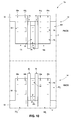
- FIGS. 8 and 9 are views of another example embodiment semiconductor device.
- FIG. 8 is a diagrammatic top view
- FIG. 9 is a diagrammatic cross-sectional side view along the line 9 - 9 of FIG. 8 .
- FIG. 10 is a diagrammatic top view of another example embodiment semiconductor device.
- FIGS. 11 and 12 are views of another example embodiment semiconductor device.
- FIG. 11 is a diagrammatic top view
- FIG. 12 is a diagrammatic cross-sectional side view along the line 12 - 12 of FIG. 11 .
- FIG. 13 is a diagrammatic top view of another example embodiment semiconductor device.
- FIG. 14 is a diagrammatic top view of another example embodiment semiconductor device.
- FIG. 15 is a diagrammatic top view of another example embodiment semiconductor device.
- Some embodiments include transistor constructions having at least two gate electrodes, and having three or more diffusion regions. At least one of the diffusion regions is longer than one or more of the other diffusion regions along a dimension corresponding to a gate width of the gate electrodes. For instance, in some embodiments source diffusion regions are formed to be longer than a drain diffusion region to reduce parasitic resistance on a source side of a transistor. Example embodiments are described below with reference to FIGS. 4-15 .
- a semiconductor device 10 is shown to comprise a PMOS region 12 paired with an NMOS region 14 .
- the PMOS region 12 includes a pair of gate electrodes 16 , and includes diffusion regions 17 - 19 adjacent the gate electrodes.
- the diffusion regions correspond to source/drain regions.
- the region 18 may be referred to as a first diffusion region between electrodes 16
- the regions 17 and 19 may be referred to as second and third diffusion regions on opposing sides of the electrodes 16 .
- the diffusion regions 17 and 19 sandwich the electrodes 16 and the first diffusion region 18 between them.
- the diffusion regions 17 - 19 correspond to source/drain regions.
- the first diffusion region 18 is a first kind corresponding to either a source region or a drain region
- the second and third diffusion regions 17 and 19 are both a second kind, different from the first kind, and corresponding to either source regions or drain regions.
- diffusion region 18 is a drain region
- diffusion regions 17 and 19 are source regions.
- the electrodes 16 have gate widths “W” extending along a direction corresponding to an axis 5 . In the shown embodiment, both electrodes have about the same gate width as one another.
- the electrodes 16 may be electrically coupled with one another, or may be operated independently of one another.
- the first diffusion region 18 has a length “L 1 ” along the direction of the gate width (i.e., along axis 5 ), and the second and third diffusion regions 17 and 19 have lengths “L 2 ” along the direction of the gate width.
- a difference between the lengths L 1 and L 2 may be within a range of from about 3 micrometers ( ⁇ m) to about 100 ⁇ m; within a range of from about 3 ⁇ m to about 50 ⁇ m; within a range of from about 3 ⁇ m to about 10 ⁇ m; within a range of from about 10 ⁇ m to about 100 ⁇ m; etc.
- the utilization of a middle diffusion region having a different length relative to outer diffusion regions in the construction of FIGS. 4-7 is an improvement which may reduce parasitic resistance on a source side of a transistor as compared to the prior art construction of FIGS. 1-3 in which the three source/drain regions 910 - 912 have the same lengths as one another.
- the gate electrodes 16 and diffusion regions 17 - 19 together form a PMOS transistor 20 (i.e., PMOS device, PMOS construction, etc.), which is approximately demarcated with a dashed line 21 .
- PMOS transistor 20 i.e., PMOS device, PMOS construction, etc.
- Each of the diffusion regions 17 - 19 has opposing edges on each side of its length. Specifically, diffusion region 17 has opposing edges 22 and 23 , diffusion region 18 has opposing edges 24 and 25 , and diffusion region 19 has opposing edges 26 and 27 .
- the PMOS transistor may be considered to have a first side 28 defined by one set of the opposing edges (for instance, edges 22 , 24 and 26 ), and to have a second side 30 defined by a second set of the opposing edges (for instance, edges 23 , 25 and 27 ). In the embodiment of FIGS.
- both of the first and second sides 28 and 30 have edges of the second diffusion region 18 (edges 24 and 25 ) inset relative to edges of the first and third diffusion regions 17 and 19 (edges 22 , 23 , 26 and 27 ).
- the inset along the first side 28 is a distance D 1
- the inset along the second side 30 is a distance D 2 .
- the distances D 1 and D 2 are about the same as one another, and accordingly the PMOS may be referred to as being H-shaped. In other embodiments, distances D 1 and D 2 may vary relative to one another.
- the distances D 1 and D 2 may be within a range of from about 1.5 ⁇ m to about 50 ⁇ m; within a range of from about 1.5 ⁇ m to about 25 ⁇ m; within a range of from about 1.5 ⁇ m to about 10 ⁇ m; within a range of from about 5 ⁇ m to about 50 ⁇ m; etc.
- Wiring 32 (for instance, WLIC1 connected to power supply voltage Vdd) is provided proximate the PMOS transistor 20 , and is electrically coupled to the outer source/drain regions 17 and 19 through contacts 33 .
- Additional wiring 34 (for instance, WLIC3) connects to the inner source/drain region 18 through contacts 35 .
- the contacts 33 and 35 may extend through insulative material 36 (shown in FIGS. 5-7 ).
- Such insulative material may comprise any suitable composition or combination of compositions; and in some embodiments may comprise, for example, one or both of silicon dioxide and silicon nitride.
- the inner diffusion region is a drain region and the outer diffusion regions are source regions.
- the drain region is placed on a side which is to be driven, and accordingly its load capacity may be set to a low level. Accordingly, the inner diffusion region may be smaller and have fewer contacts than the outer diffusion regions.
- the NMOS region 14 includes a pair of gate electrodes 36 , and includes diffusion regions 37 - 39 adjacent the gate electrodes.
- the electrodes 36 may be electrically coupled with one another, or may be operated independently of one another.
- the region 38 may be referred to as a first diffusion region between electrodes 36
- the regions 37 and 39 may be referred to as second and third diffusion regions on opposing sides of the electrodes 36 .
- the diffusion regions 37 and 39 sandwich the electrodes 36 and the first diffusion region 38 between them.
- the regions 37 - 39 may be referred to as fourth-sixth diffusion regions, respectively, in that the regions 17 - 19 of the PMOS are already referred to as the first-third diffusion regions.
- the diffusion regions 37 - 39 correspond to source/drain regions.
- the diffusion region 38 is a first kind corresponding to either a source region or a drain region, and the diffusion regions 37 and 39 are both a second kind, different from the first kind, and corresponding to either source regions or drain regions.
- diffusion region 38 is a drain region, and diffusion regions 37 and 39 are source regions.
- the electrodes 36 have gate widths “W 1 ” extending along the direction corresponding to the axis 5 . In the shown embodiment, both electrodes have about the same gate width as one another. In some embodiments, the width W 1 of the gate electrodes of NMOS device 40 may be referred to as a second width to distinguish it from the first width W of the gate electrodes of the PMOS device 20 ,
- the diffusion region 38 has a length “L 3 ” along the direction of the gate width W 1 (i.e., along axis 5 ), and the diffusion regions 37 and 39 have lengths “L 4 ” along the direction of the gate width.
- a difference between the lengths L 3 and L 4 may be within a range of from about 3 ⁇ m to about 100 ⁇ m; within a range of from about 3 ⁇ m to about 50 ⁇ m; within a range of from about 3 ⁇ m to about 10 ⁇ m; within a range of from about 10 ⁇ m to about 100 ⁇ m; etc.
- the utilization of a middle diffusion region having a different length relative to outer diffusion regions may reduce parasitic resistance on a source side of a transistor as compared to conventional constructions.
- NMOS transistor 40 i.e., NMOS device, NMOS construction, etc.
- Each of the diffusion regions 37 - 39 has opposing edges on each side of its length. Specifically, diffusion region 37 has opposing edges 42 and 43 , diffusion region 38 has opposing edges 44 and 45 , and diffusion region 39 has opposing edges 46 and 47 .
- the NMOS transistor may be considered to have a first side 48 defined by one set of the opposing edges (for instance, edges 42 , 44 and 46 ), and to have a second side 50 defined by a second set of the opposing edges (for instance, edges 43 , 45 and 47 ). In the embodiment of FIGS.
- both of the first and second sides 48 and 50 have edges of the second diffusion region 38 (edges 44 and 45 ) inset relative to edges of the first and third diffusion regions 37 and 39 (edges 42 , 43 , 46 and 47 ).
- the inset along the first side 48 is a distance D 3
- the inset along the second side 50 is a distance D 4 .
- the distances D 3 and D 4 are about the same as one another, and accordingly the NMOS may be referred to as being H-shaped. In other embodiments, distances D 3 and D 4 may vary relative to one another.
- the distances D 3 and D 4 may be within a range of from about 1.5 ⁇ m to about 50 ⁇ m; within a range of from about 1.5 ⁇ m to about 25 ⁇ m; within a range of from about 1.5 ⁇ m to about 10 ⁇ m; within a range of from about 5 ⁇ m to about 50 ⁇ m; etc.
- Wiring 52 (for instance, WLIC2 connected to power supply voltage Vss) is provided proximate the NMOS transistor 40 , and is electrically coupled to the outer source/drain regions 37 and 39 through contacts 53 .
- Additional wiring 54 (for instance, WLIC3) connects to the inner source/drain region 38 through contacts 55 .
- the inner diffusion region is a drain region and the outer diffusion regions are source regions.
- the drain region is placed on a side which is to be driven, and accordingly its load capacity may be set to a low level. Accordingly, the inner diffusion region may be smaller and have fewer contacts than the outer diffusion regions.
- wirings 32 and 52 may comprise first and second wiring lines, respectively. Such wiring lines may supply first and second power voltages, respectively. The first and second power voltages may be different relative to one another during operation of the construction comprising the PMOS device 12 and NMOS device 14 .
- the wiring 34 of PMOS device 20 and the wiring 54 of NMOS device 40 correspond to a common wiring line. Accordingly, in some embodiments the contacts 33 couple outer diffusion regions 17 and 19 of PMOS device 20 to a first wiring line 32 , the contacts 53 couple outer diffusion regions 37 and 39 of NMOS device 40 to a second wiring line 52 , and the contacts 35 and 55 couple the diffusion regions 18 and 38 of the PMOS and NMOS devices to a third wiring line comprising regions 34 and 54 .
- the PMOS and NMOS regions 12 and 14 are supported by a base 56 (shown in FIGS. 5-7 ).
- the base 56 may comprise semiconductor material; and may, for example, comprise, consist essentially of, or consist of monocrystalline silicon.
- the base 56 may be referred to as a semiconductor substrate.
- semiconductor substrate means any construction comprising semiconductive material, including, but not limited to, bulk semiconductive materials such as a semiconductive wafer (either alone or in assemblies comprising other materials), and semiconductive material layers (either alone or in assemblies comprising other materials).
- substrate refers to any supporting structure, including, but not limited to, the semiconductor substrates described above.
- the base 56 may correspond to a semiconductor substrate containing one or more materials associated with integrated circuit fabrication. Such materials may include, for example, one or more of refractory metal materials, barrier materials, diffusion materials, insulator materials, etc.
- the semiconductor substrate 56 is shown to comprise a p-type background-doped region 58 , and to comprise an n-type doped n-well 60 extending into the p-type doped region.
- the diffusion regions 17 - 19 of the PMOS device are within the n-well 60 ; and the diffusion regions 37 - 39 of the NMOS are within the p-type background-doped region 58 .
- the diffusion regions 17 - 19 of PMOS device 20 are of a first conductivity type (specifically, p-type) and the diffusion regions 37 - 39 of NMOS device 40 are of a second conductivity type (specifically, n-type); with the second conductivity type being different from the first conductivity type.
- FIGS. 8 and 9 show a semiconductor device 10 a illustrating another embodiment.
- Semiconductor device (i.e., construction) 10 a includes a PMOS region 12 paired with an NMOS region 14 .
- a PMOS device 20 a is within region 12
- an NMOS device 40 a is within region 14
- the PMOS device comprises diffusion regions 17 - 19 analogous to the regions described above with reference to FIGS. 4-7
- the NMOS device comprises diffusion regions 37 - 39 analogous to the regions described above with reference to FIGS. 4-7
- Each of the PMOS diffusion regions comprises opposing edges along the length of the region; with region 17 having edges 22 and 23 , region 18 having edges 24 and 25 , and region 19 having edges 26 and 27 .
- each of the NMOS diffusion regions comprises opposing edges along the length of the region; with region 37 having edges 42 and 43 , region 38 having edges 44 and 45 , and region 39 having edges 46 and 47 .
- edges 22 , 24 and 26 form a first side 28 a of the device 20 a ; and the edges 23 , 25 and 27 form a second side 30 a of the device 20 a .
- the edges 42 , 44 and 46 form a first side 48 a of the device 40 a
- the edges 43 , 45 and 47 form a second side 50 a of the device 40 a.
- the construction 10 a of FIGS. 8 and 9 like the construction 10 of FIGS. 4-7 , has the middle diffusion regions of the PMOS and NMOS devices (regions 18 and 38 ) shorter than the outer diffusion regions of the devices (regions 17 , 19 , 37 and 39 ).
- a difference between the construction of FIGS. 8 and 9 relative to that of FIGS. 4-7 is that the edges along first side 28 a of the PMOS device 20 a are approximately even with one another (i.e., are offset from one another by less than or equal to about 2 ⁇ m; in some embodiments offset from one another by less than or equal to about 1 ⁇ m; and in some embodiments offset from one another by less than or equal to about 0.5 ⁇ m), rather than being staggered like the edges along the first side 28 of the PMOS device 20 ( FIG. 4 ).
- the edges along the second side 30 a of PMOS device 20 a are staggered similarly to the edges along the second side 30 of PMOS device 20 ( FIG.
- D 5 of FIG. 8 may be about twice as large as D 2 of FIG. 4 due to there being very little inset (in some embodiments, no inset or even some minor outset) along the side 28 a of device 20 a .
- D 5 may be within a range of from about 3 ⁇ m to about 100 ⁇ m; within a range of from about 3 ⁇ m to about 50 ⁇ m; within a range of from about 3 ⁇ m to about 20 ⁇ m; within a range of from about 10 ⁇ m to about 100 ⁇ m; etc.
- edges along second side 50 a of the NMOS device 40 a are approximately even with one another (i.e., are offset from one another by less than or equal to about 2 ⁇ m; in some embodiments offset from one another by less than or equal to about 1 ⁇ m; and in some embodiments offset from one another by less than or equal to about 0.5 ⁇ m), rather than being staggered like the edges along the second side 50 of the NMOS device 40 ( FIG. 4 ).
- the edges along the first side 48 a of NMOS device 40 a are staggered similarly to the edges along the first side 48 of NMOS device 40 ( FIG.
- D 6 of FIG. 8 may be about twice as large as D 3 of FIG. 4 due to there being very little inset (in some embodiments, no inset or even some minor outset) along the side 50 a of device 20 a .
- D 6 may be within a range of from about 3 nm to about 100 ⁇ m; within a range of from about 3 ⁇ m to about 50 ⁇ m; within a range of from about 3 ⁇ m to about 20 ⁇ m; within a range of from about 10 ⁇ m to about 100 ⁇ m; etc.
- the PMOS and NMOS devices 20 and 40 of the construction 10 of FIG. 4 may be referred to as being H-shaped
- those of construction 10 a of FIG. 8 i.e., devices 20 a and 40 a
- the construction 10 a of FIG. 8 may enable higher integration than the construction 10 of FIG. 4 , at least in part due to increased overlap of the wirings 32 and 52 across source/drain diffusion regions of transistor devices 20 a and 40 a . It can be desired to maintain the illustrated gaps between inner diffusion regions 18 and 38 and the respective wirings 32 and 52 to avoid undesired deterioration of transistor characteristics.
- the contacts 33 within outer diffusion regions 17 and 19 of PMOS device 20 a are arranged in single columns 62 and 64 ; and similarly the contacts 53 within outer diffusion regions 37 and 39 of NMOS device 40 a are arranged in single columns 66 and 68 .
- the contacts 35 within inner diffusion region 18 of the PMOS device arranged in a single column 63 and the contacts within inner diffusion region 38 of the NMOS device are arranged in a single column 65 .
- FIG. 10 shows a construction 10 b comprising PMOS and NMOS devices 20 b and 40 b similar to the devices 20 a and 40 a of FIG. 8 .
- the contacts 33 within diffusion regions 17 b and 19 b of the PMOS device are arranged in multiple columns 62 a , 62 b , 64 a and 64 b ; and similarly the contacts 53 within diffusion regions 37 b and 39 b are arranged in multiple columns 66 a , 66 b , 68 a and 68 b.
- the contacts within inner diffusion regions 18 b and 38 b remain arranged in single columns, but different configurations may be utilized in other embodiments.
- the configuration of FIG. 10 may be considered to increase the size of the outer diffusion regions ( 17 b , 19 b , 37 b and 39 b ) by increasing the width of such outer diffusion regions; and in the shown embodiment the outer diffusion regions have both increased width and increased length as compared to the inner diffusion regions ( 18 b and 38 b )
- FIG. 4 has an equal number of diffusion regions associated with PMOS device 20 (three) as are associated with NMOS device 40 .
- the PMOS device may have a different number of diffusion regions than the NMOS device.
- FIG. 11 shows an example construction 10 c in which a PMOS device 20 c comprises five diffusion regions, and an NMOS device 40 c comprises three diffusion regions; and such construction may correspond to, for example, an inverter.
- the diffusion regions may be referred to as first, second, third, fourth, fifth, sixth, seventh and eighth diffusion regions.
- the PMOS device 20 c may be considered to comprise first, second and third diffusion regions 17 c - 19 c analogous to the regions 17 - 19 of FIG.
- the NMOS device 40 c may be considered to comprise fourth, fifth and sixth diffusion regions 37 - 39 identical to the regions 37 - 39 of FIG. 4 .
- the PMOS device may be considered to comprise seventh and eighth diffusion regions 70 and 72 , with the seventh diffusion region 70 being about the same length as diffusion region 18 c , and the eighth diffusion 72 being about the same length as diffusion regions 17 c and 19 c.
- wiring 34 extends across all of the shorter diffusion regions 70 , 18 c and 38 in the embodiment of FIG. 7 ; wiring 32 is connected with the longer PMOS diffusion regions 17 c , 19 c and 72 ; and wiring 52 is connected with the longer NMOS diffusion regions 37 and 29 . Also, gates 16 of the PMOS device are electrically coupled with the gates 36 of the NMOS device.
- the PMOS transistor have increased channel width as compared to the NMOS transistor due to differences in the mobility of carriers (for instance, in some embodiments the PMOS transistor may have a channel width about two-times greater than the channel width of the NMOS transistor).
- the arrangement of FIG. 11 may effectively create a greater channel width for the PMOS transistor.
- FIG. 12 shows a cross-section through the PMOS device 20 c of FIG. 11 to illustrate elevational relationships of various structures.
- FIG. 11 comprises staggered sides 28 and 30 of the PMOS device 20 c analogous to the staggered sites 28 and 30 of the construction of FIG. 4 , and comprises staggered sides 48 and 50 of NMOS construction 40 c analogous to the staggered sides 48 and 50 of the construction of FIG. 4 .
- constructions similar to that of FIG. 11 may be formed to have even sides analogous to those described above with reference to FIG. 8 .
- FIG. 13 shows a construction 10 d having PMOS and NMOS structures 20 d and 40 d analogous to the structures 20 c and 40 c of FIG. 11 , but having even sides 28 and 50 rather than the staggered sides shown in FIG. 11 .
- FIG. 4 comprises an equal number of contacts within NMOS regions 37 , 38 and 39 as are in PMOS regions 17 , 18 and 19 , respectively.
- the NMOS and PMOS regions may have other configurations.
- FIG. 14 shows a construction 10 e which is analogous to the construction 10 of FIG. 4 , but in which regions 17 , 18 and 19 are longer than regions 37 , 38 and 39 , respectively; and have more contacts than regions 37 , 38 and 39 , respectively (i.e., more contacts 33 and 35 to the respective regions than there are contacts 53 and 55 to the respective regions).
- the embodiment of FIG. 14 may enable, for example, a PMOS device to be formed with a larger channel width than an adjacent NMOS device, or vice versa.
- FIG. 14 comprises staggered sides of the PMOS and NMOS transistors analogous to the staggered sides 28 , 30 , 48 and 50 of FIG. 4 .
- FIG. 15 shows another example embodiment, and specifically shows a construction 10 f similar to the construction of FIG. 14 but in which each of the PMOS and NMOS transistors has a non-staggered (i.e., even) side analogous to the construction described above with reference to FIG. 8 .
- the number of contacts to various diffusion regions may be tailored to achieve desired speed/voltage characteristics, while also striving to keep device footprint small.
- diffusion regions of the embodiments of FIGS. 11, 13, 14 and 15 may have increased width as well as length (i.e., may include aspects shown in FIG. 10 ) in some embodiments.
- the devices discussed above may be incorporated into electronic systems.
- Such electronic systems may be used in, for example, logic, memory modules, device drivers, power modules, communication modems, processor modules, and application-specific modules, and may include multilayer, multichip modules.
- the electronic systems may be any of a broad range of systems, such as, for example, cameras, wireless devices, displays, chip sets, set top boxes, games, lighting, vehicles, clocks, televisions, cell phones, personal computers, automobiles, industrial control systems, aircraft, etc.
- the various materials, substances, compositions, etc. described herein may be formed with any suitable methodologies, either now known or yet to be developed, including, for example, atomic layer deposition (ALD), chemical vapor deposition (CVD), physical vapor deposition (PVD), etc.
- ALD atomic layer deposition
- CVD chemical vapor deposition
- PVD physical vapor deposition
- Some embodiments include a semiconductor device having two gate electrodes which are of about a same gate width as one another, and a first diffusion region between the two gate electrodes.
- the first diffusion region is a first source/drain region.
- the semiconductor devices also has second and third diffusion regions on opposing sides of the two gate electrodes from one another and which sandwich the two gate electrodes and the first source/drain region therebetween.
- the second and third diffusion regions are second and third source/drain regions, respectively.
- the first source/drain region is a first kind of region corresponding to either a source region or a drain region.
- the second and third source/drain regions are a second kind of region different from the first kind and either both being source regions or both being drain regions.
- Each of the second and third diffusion regions is longer than the first diffusion region in a direction of the gate width.
- Some embodiments include a semiconductor device comprising a PMOS construction and an NMOS construction.
- the PMOS construction includes two first gate electrodes having a first gate width, a first diffusion region between the first gate electrodes, and second and third diffusion regions on opposing sides of the first gate electrodes from one another and which sandwich the first gate electrodes and the first diffusion region therebetween. Each of the second and third diffusion regions is longer than the first diffusion region in a direction of the first gate width.
- the NMOS construction includes two second gate electrodes having a second gate width, a fourth diffusion region between the second gate electrodes, and fifth and sixth diffusion regions on opposing sides of the second gate electrodes from one another and which sandwich the second gate electrodes and the fourth diffusion region therebetween. Each of the fifth and sixth diffusion regions is longer than the fourth diffusion region in a direction of the second gate width.
- Some embodiments include a semiconductor device comprising a first wiring line extending along a first direction, a second wiring line extending along the first direction, a PMOS construction, and an NMOS construction.
- the PMOS construction includes a first transistor having two first gate electrodes of about a same gate width as one another, with the gate width of the two first gate electrodes being a first gate width.
- the PMOS construction also includes a first diffusion region between the two first gate electrodes, and second and third diffusion regions on opposing sides of the two first gate electrodes from one another and which sandwich the two first gate electrodes and the first diffusion region therebetween. Each of the second and third diffusion regions is longer than the first diffusion region in a direction of the first gate width.
- the first, second and third diffusion regions are of a first conductivity type.
- the second and third diffusion regions are electrically coupled with the first wiring line.
- the NMOS construction includes a second transistor having two second gate electrodes of about a same gate width as one another, with the gate width of the two second gate electrodes being a second gate width.
- the NMOS construction also includes a fourth diffusion region between the two second gate electrodes, and fifth and sixth diffusion regions on opposing sides of the two second gate electrodes from one another and which sandwich the two second gate electrodes and the fourth diffusion region therebetween.
- Each of the fifth and sixth diffusion regions is longer than the fourth diffusion region in a direction of the second gate width.
- the fourth, fifth and sixth diffusion regions are of a second conductivity type different from the first conductivity type.
- the fifth and sixth diffusion regions are electrically coupled with the second wiring line.
Abstract
Description
Claims (21)
Priority Applications (1)
| Application Number | Priority Date | Filing Date | Title |
|---|---|---|---|
| US14/750,139 US9461045B1 (en) | 2015-06-25 | 2015-06-25 | Semiconductor devices |
Applications Claiming Priority (1)
| Application Number | Priority Date | Filing Date | Title |
|---|---|---|---|
| US14/750,139 US9461045B1 (en) | 2015-06-25 | 2015-06-25 | Semiconductor devices |
Publications (1)
| Publication Number | Publication Date |
|---|---|
| US9461045B1 true US9461045B1 (en) | 2016-10-04 |
Family
ID=56995189
Family Applications (1)
| Application Number | Title | Priority Date | Filing Date |
|---|---|---|---|
| US14/750,139 Active US9461045B1 (en) | 2015-06-25 | 2015-06-25 | Semiconductor devices |
Country Status (1)
| Country | Link |
|---|---|
| US (1) | US9461045B1 (en) |
Citations (7)
| Publication number | Priority date | Publication date | Assignee | Title |
|---|---|---|---|---|
| US5812443A (en) | 1995-06-09 | 1998-09-22 | Hyundai Electronics Industries Co., Ltd. | Memory integrated circuit and methods for manufacturing the same |
| US7034364B2 (en) * | 2004-05-25 | 2006-04-25 | Texas Instruments Incorporated | Reduced finger end MOSFET breakdown voltage (BV) for electrostatic discharge (ESD) protection |
| US7323727B2 (en) | 1995-11-09 | 2008-01-29 | Hitachi, Ltd. | System with meshed power and signal buses on cell array |
| US7511345B2 (en) * | 2005-06-21 | 2009-03-31 | Sarnoff Corporation | Bulk resistance control technique |
| US7691713B2 (en) | 2003-05-21 | 2010-04-06 | Renesas Technology Corp. | Method of manufacturing semiconductor device capable of suppressing impurity concentration reduction in doped channel region arising from formation of gate insulating film |
| US8569841B2 (en) * | 2008-03-13 | 2013-10-29 | Tela Innovations, Inc. | Integrated circuit including cross-coupled transistors having gate electrodes formed within gate level feature layout channels with at least one gate level feature extending into adjacent gate level feature layout channel |
| US20150035054A1 (en) | 2013-08-01 | 2015-02-05 | Micron Technology, Inc. | Semiconductor device |
-
2015
- 2015-06-25 US US14/750,139 patent/US9461045B1/en active Active
Patent Citations (7)
| Publication number | Priority date | Publication date | Assignee | Title |
|---|---|---|---|---|
| US5812443A (en) | 1995-06-09 | 1998-09-22 | Hyundai Electronics Industries Co., Ltd. | Memory integrated circuit and methods for manufacturing the same |
| US7323727B2 (en) | 1995-11-09 | 2008-01-29 | Hitachi, Ltd. | System with meshed power and signal buses on cell array |
| US7691713B2 (en) | 2003-05-21 | 2010-04-06 | Renesas Technology Corp. | Method of manufacturing semiconductor device capable of suppressing impurity concentration reduction in doped channel region arising from formation of gate insulating film |
| US7034364B2 (en) * | 2004-05-25 | 2006-04-25 | Texas Instruments Incorporated | Reduced finger end MOSFET breakdown voltage (BV) for electrostatic discharge (ESD) protection |
| US7511345B2 (en) * | 2005-06-21 | 2009-03-31 | Sarnoff Corporation | Bulk resistance control technique |
| US8569841B2 (en) * | 2008-03-13 | 2013-10-29 | Tela Innovations, Inc. | Integrated circuit including cross-coupled transistors having gate electrodes formed within gate level feature layout channels with at least one gate level feature extending into adjacent gate level feature layout channel |
| US20150035054A1 (en) | 2013-08-01 | 2015-02-05 | Micron Technology, Inc. | Semiconductor device |
Similar Documents
| Publication | Publication Date | Title |
|---|---|---|
| US11735479B2 (en) | Assemblies containing PMOS decks vertically-integrated with NMOS decks, and methods of forming integrated assemblies | |
| US9966376B2 (en) | Semiconductor devices and inverter having the same | |
| US6924560B2 (en) | Compact SRAM cell with FinFET | |
| CN105023605B (en) | The connection structure of vertical loopful grid (VGAA) device on semiconductor-on-insulator (SOI) substrate | |
| US8618607B1 (en) | Semiconductor devices formed on a continuous active region with an isolating conductive structure positioned between such semiconductor devices, and methods of making same | |
| US9935100B2 (en) | Power rail inbound middle of line (MOL) routing | |
| US20090067220A1 (en) | Semiconductor device including memory having nodes connected with continuous diffusion layer but isolated from each other by transistor | |
| US9721951B2 (en) | Semiconductor device using Ge channel and manufacturing method thereof | |
| US10411085B2 (en) | Semiconductor device and a method for fabricating the same | |
| US10453840B2 (en) | Semiconductor integrated circuit | |
| US10971581B2 (en) | Semiconductor device | |
| US10950545B2 (en) | Circuit wiring techniques for stacked transistor structures | |
| US10461150B2 (en) | Semiconductor device | |
| US20220045215A1 (en) | Semiconductor device | |
| US20180175047A1 (en) | Semiconductor device | |
| EP0426174B1 (en) | Semiconductor integrated circuit | |
| WO2016207930A1 (en) | Semiconductor device | |
| CN113767466A (en) | Semiconductor device with a plurality of semiconductor chips | |
| CN107026158B (en) | Trench-based charge pump device | |
| US7884424B2 (en) | Structure of MTCMOS cell | |
| US20210366902A1 (en) | Semiconductor integrated circuit device | |
| US9461045B1 (en) | Semiconductor devices | |
| US6979870B2 (en) | Semiconductor integrated circuit including CMOS logic gate | |
| US10410934B2 (en) | Apparatuses having an interconnect extending from an upper conductive structure, through a hole in another conductive structure, and to an underlying structure | |
| KR20160092923A (en) | Vertical type cmos inverter device |
Legal Events
| Date | Code | Title | Description |
|---|---|---|---|
| AS | Assignment |
Owner name: MICRON TECHNOLOGY, INC., IDAHO Free format text: ASSIGNMENT OF ASSIGNORS INTEREST;ASSIGNORS:ASANO, SHINTARO;SAKITO, YUSUKE;REEL/FRAME:035966/0664 Effective date: 20150625 |
|
| AS | Assignment |
Owner name: U.S. BANK NATIONAL ASSOCIATION, AS COLLATERAL AGENT, CALIFORNIA Free format text: SECURITY INTEREST;ASSIGNOR:MICRON TECHNOLOGY, INC.;REEL/FRAME:038669/0001 Effective date: 20160426 Owner name: U.S. BANK NATIONAL ASSOCIATION, AS COLLATERAL AGEN Free format text: SECURITY INTEREST;ASSIGNOR:MICRON TECHNOLOGY, INC.;REEL/FRAME:038669/0001 Effective date: 20160426 |
|
| AS | Assignment |
Owner name: MORGAN STANLEY SENIOR FUNDING, INC., AS COLLATERAL AGENT, MARYLAND Free format text: PATENT SECURITY AGREEMENT;ASSIGNOR:MICRON TECHNOLOGY, INC.;REEL/FRAME:038954/0001 Effective date: 20160426 Owner name: MORGAN STANLEY SENIOR FUNDING, INC., AS COLLATERAL Free format text: PATENT SECURITY AGREEMENT;ASSIGNOR:MICRON TECHNOLOGY, INC.;REEL/FRAME:038954/0001 Effective date: 20160426 |
|
| STCF | Information on status: patent grant |
Free format text: PATENTED CASE |
|
| AS | Assignment |
Owner name: U.S. BANK NATIONAL ASSOCIATION, AS COLLATERAL AGENT, CALIFORNIA Free format text: CORRECTIVE ASSIGNMENT TO CORRECT THE REPLACE ERRONEOUSLY FILED PATENT #7358718 WITH THE CORRECT PATENT #7358178 PREVIOUSLY RECORDED ON REEL 038669 FRAME 0001. ASSIGNOR(S) HEREBY CONFIRMS THE SECURITY INTEREST;ASSIGNOR:MICRON TECHNOLOGY, INC.;REEL/FRAME:043079/0001 Effective date: 20160426 Owner name: U.S. BANK NATIONAL ASSOCIATION, AS COLLATERAL AGEN Free format text: CORRECTIVE ASSIGNMENT TO CORRECT THE REPLACE ERRONEOUSLY FILED PATENT #7358718 WITH THE CORRECT PATENT #7358178 PREVIOUSLY RECORDED ON REEL 038669 FRAME 0001. ASSIGNOR(S) HEREBY CONFIRMS THE SECURITY INTEREST;ASSIGNOR:MICRON TECHNOLOGY, INC.;REEL/FRAME:043079/0001 Effective date: 20160426 |
|
| AS | Assignment |
Owner name: JPMORGAN CHASE BANK, N.A., AS COLLATERAL AGENT, ILLINOIS Free format text: SECURITY INTEREST;ASSIGNORS:MICRON TECHNOLOGY, INC.;MICRON SEMICONDUCTOR PRODUCTS, INC.;REEL/FRAME:047540/0001 Effective date: 20180703 Owner name: JPMORGAN CHASE BANK, N.A., AS COLLATERAL AGENT, IL Free format text: SECURITY INTEREST;ASSIGNORS:MICRON TECHNOLOGY, INC.;MICRON SEMICONDUCTOR PRODUCTS, INC.;REEL/FRAME:047540/0001 Effective date: 20180703 |
|
| AS | Assignment |
Owner name: MICRON TECHNOLOGY, INC., IDAHO Free format text: RELEASE BY SECURED PARTY;ASSIGNOR:U.S. BANK NATIONAL ASSOCIATION, AS COLLATERAL AGENT;REEL/FRAME:047243/0001 Effective date: 20180629 |
|
| AS | Assignment |
Owner name: MICRON TECHNOLOGY, INC., IDAHO Free format text: RELEASE BY SECURED PARTY;ASSIGNOR:MORGAN STANLEY SENIOR FUNDING, INC., AS COLLATERAL AGENT;REEL/FRAME:050937/0001 Effective date: 20190731 |
|
| AS | Assignment |
Owner name: MICRON TECHNOLOGY, INC., IDAHO Free format text: RELEASE BY SECURED PARTY;ASSIGNOR:JPMORGAN CHASE BANK, N.A., AS COLLATERAL AGENT;REEL/FRAME:051028/0001 Effective date: 20190731 Owner name: MICRON SEMICONDUCTOR PRODUCTS, INC., IDAHO Free format text: RELEASE BY SECURED PARTY;ASSIGNOR:JPMORGAN CHASE BANK, N.A., AS COLLATERAL AGENT;REEL/FRAME:051028/0001 Effective date: 20190731 |
|
| MAFP | Maintenance fee payment |
Free format text: PAYMENT OF MAINTENANCE FEE, 4TH YEAR, LARGE ENTITY (ORIGINAL EVENT CODE: M1551); ENTITY STATUS OF PATENT OWNER: LARGE ENTITY Year of fee payment: 4 |
|
| MAFP | Maintenance fee payment |
Free format text: PAYMENT OF MAINTENANCE FEE, 8TH YEAR, LARGE ENTITY (ORIGINAL EVENT CODE: M1552); ENTITY STATUS OF PATENT OWNER: LARGE ENTITY Year of fee payment: 8 |