US9461001B1 - Semiconductor device package integrated with coil for wireless charging and electromagnetic interference shielding, and method of manufacturing the same - Google Patents
Semiconductor device package integrated with coil for wireless charging and electromagnetic interference shielding, and method of manufacturing the same Download PDFInfo
- Publication number
- US9461001B1 US9461001B1 US14/805,847 US201514805847A US9461001B1 US 9461001 B1 US9461001 B1 US 9461001B1 US 201514805847 A US201514805847 A US 201514805847A US 9461001 B1 US9461001 B1 US 9461001B1
- Authority
- US
- United States
- Prior art keywords
- magnetic
- disposed
- conductive layer
- shield
- top surface
- Prior art date
- Legal status (The legal status is an assumption and is not a legal conclusion. Google has not performed a legal analysis and makes no representation as to the accuracy of the status listed.)
- Active
Links
Images


Classifications
-
- H—ELECTRICITY
- H01—ELECTRIC ELEMENTS
- H01L—SEMICONDUCTOR DEVICES NOT COVERED BY CLASS H10
- H01L23/00—Details of semiconductor or other solid state devices
- H01L23/552—Protection against radiation, e.g. light or electromagnetic waves
-
- H10W42/20—
-
- H—ELECTRICITY
- H01—ELECTRIC ELEMENTS
- H01F—MAGNETS; INDUCTANCES; TRANSFORMERS; SELECTION OF MATERIALS FOR THEIR MAGNETIC PROPERTIES
- H01F1/00—Magnets or magnetic bodies characterised by the magnetic materials therefor; Selection of materials for their magnetic properties
-
- H—ELECTRICITY
- H01—ELECTRIC ELEMENTS
- H01L—SEMICONDUCTOR DEVICES NOT COVERED BY CLASS H10
- H01L21/00—Processes or apparatus adapted for the manufacture or treatment of semiconductor or solid state devices or of parts thereof
- H01L21/02—Manufacture or treatment of semiconductor devices or of parts thereof
- H01L21/04—Manufacture or treatment of semiconductor devices or of parts thereof the devices having potential barriers, e.g. a PN junction, depletion layer or carrier concentration layer
- H01L21/48—Manufacture or treatment of parts, e.g. containers, prior to assembly of the devices, using processes not provided for in a single one of the groups H01L21/18 - H01L21/326 or H10D48/04 - H10D48/07
- H01L21/4814—Conductive parts
- H01L21/4817—Conductive parts for containers, e.g. caps
-
- H—ELECTRICITY
- H01—ELECTRIC ELEMENTS
- H01L—SEMICONDUCTOR DEVICES NOT COVERED BY CLASS H10
- H01L21/00—Processes or apparatus adapted for the manufacture or treatment of semiconductor or solid state devices or of parts thereof
- H01L21/02—Manufacture or treatment of semiconductor devices or of parts thereof
- H01L21/04—Manufacture or treatment of semiconductor devices or of parts thereof the devices having potential barriers, e.g. a PN junction, depletion layer or carrier concentration layer
- H01L21/50—Assembly of semiconductor devices using processes or apparatus not provided for in a single one of the groups H01L21/18 - H01L21/326 or H10D48/04 - H10D48/07 e.g. sealing of a cap to a base of a container
- H01L21/52—Mounting semiconductor bodies in containers
-
- H—ELECTRICITY
- H01—ELECTRIC ELEMENTS
- H01L—SEMICONDUCTOR DEVICES NOT COVERED BY CLASS H10
- H01L21/00—Processes or apparatus adapted for the manufacture or treatment of semiconductor or solid state devices or of parts thereof
- H01L21/02—Manufacture or treatment of semiconductor devices or of parts thereof
- H01L21/04—Manufacture or treatment of semiconductor devices or of parts thereof the devices having potential barriers, e.g. a PN junction, depletion layer or carrier concentration layer
- H01L21/50—Assembly of semiconductor devices using processes or apparatus not provided for in a single one of the groups H01L21/18 - H01L21/326 or H10D48/04 - H10D48/07 e.g. sealing of a cap to a base of a container
- H01L21/56—Encapsulations, e.g. encapsulation layers, coatings
-
- H—ELECTRICITY
- H01—ELECTRIC ELEMENTS
- H01L—SEMICONDUCTOR DEVICES NOT COVERED BY CLASS H10
- H01L21/00—Processes or apparatus adapted for the manufacture or treatment of semiconductor or solid state devices or of parts thereof
- H01L21/70—Manufacture or treatment of devices consisting of a plurality of solid state components formed in or on a common substrate or of parts thereof; Manufacture of integrated circuit devices or of parts thereof
- H01L21/71—Manufacture of specific parts of devices defined in group H01L21/70
- H01L21/768—Applying interconnections to be used for carrying current between separate components within a device comprising conductors and dielectrics
- H01L21/76838—Applying interconnections to be used for carrying current between separate components within a device comprising conductors and dielectrics characterised by the formation and the after-treatment of the conductors
- H01L21/76886—Modifying permanently or temporarily the pattern or the conductivity of conductive members, e.g. formation of alloys, reduction of contact resistances
- H01L21/76892—Modifying permanently or temporarily the pattern or the conductivity of conductive members, e.g. formation of alloys, reduction of contact resistances modifying the pattern
-
- H—ELECTRICITY
- H01—ELECTRIC ELEMENTS
- H01L—SEMICONDUCTOR DEVICES NOT COVERED BY CLASS H10
- H01L23/00—Details of semiconductor or other solid state devices
- H01L23/02—Containers; Seals
- H01L23/04—Containers; Seals characterised by the shape of the container or parts, e.g. caps, walls
-
- H—ELECTRICITY
- H01—ELECTRIC ELEMENTS
- H01L—SEMICONDUCTOR DEVICES NOT COVERED BY CLASS H10
- H01L23/00—Details of semiconductor or other solid state devices
- H01L23/28—Encapsulations, e.g. encapsulating layers, coatings, e.g. for protection
- H01L23/31—Encapsulations, e.g. encapsulating layers, coatings, e.g. for protection characterised by the arrangement or shape
- H01L23/3107—Encapsulations, e.g. encapsulating layers, coatings, e.g. for protection characterised by the arrangement or shape the device being completely enclosed
-
- H—ELECTRICITY
- H01—ELECTRIC ELEMENTS
- H01L—SEMICONDUCTOR DEVICES NOT COVERED BY CLASS H10
- H01L23/00—Details of semiconductor or other solid state devices
- H01L23/52—Arrangements for conducting electric current within the device in operation from one component to another, i.e. interconnections, e.g. wires, lead frames
- H01L23/538—Arrangements for conducting electric current within the device in operation from one component to another, i.e. interconnections, e.g. wires, lead frames the interconnection structure between a plurality of semiconductor chips being formed on, or in, insulating substrates
- H01L23/5386—Geometry or layout of the interconnection structure
-
- H—ELECTRICITY
- H01—ELECTRIC ELEMENTS
- H01L—SEMICONDUCTOR DEVICES NOT COVERED BY CLASS H10
- H01L23/00—Details of semiconductor or other solid state devices
- H01L23/58—Structural electrical arrangements for semiconductor devices not otherwise provided for, e.g. in combination with batteries
- H01L23/64—Impedance arrangements
- H01L23/645—Inductive arrangements
-
- H—ELECTRICITY
- H02—GENERATION; CONVERSION OR DISTRIBUTION OF ELECTRIC POWER
- H02J—CIRCUIT ARRANGEMENTS OR SYSTEMS FOR SUPPLYING OR DISTRIBUTING ELECTRIC POWER; SYSTEMS FOR STORING ELECTRIC ENERGY
- H02J50/00—Circuit arrangements or systems for wireless supply or distribution of electric power
- H02J50/10—Circuit arrangements or systems for wireless supply or distribution of electric power using inductive coupling
-
- H02J7/025—
-
- H10W42/276—
-
- H10W42/287—
-
- H10W44/501—
-
- H10W70/092—
-
- H10W70/093—
-
- H10W70/095—
-
- H10W70/611—
-
- H10W70/635—
-
- H10W70/65—
-
- H10W74/016—
-
- H10W74/129—
-
- H10W76/01—
-
- H10W90/00—
-
- H10W90/293—
-
- H10W90/701—
-
- H10W72/252—
-
- H10W74/00—
-
- H10W74/10—
-
- H10W76/12—
-
- H10W90/724—
-
- H10W90/754—
Definitions
- the present disclosure relates generally to semiconductor device packages and the manufacturing methods thereof. More particularly, the present disclosure relates to semiconductor device packages integrated with coils for wireless charging and integrated with shields for electromagnetic interference shielding, and the manufacturing methods thereof.
- Electromagnetic emissions can radiate from a source semiconductor device, and can be incident upon neighboring semiconductor devices. If the level of electromagnetic emissions at a neighboring semiconductor device is sufficiently high, these emissions can adversely affect the operation of that semiconductor device. This phenomenon is sometimes referred to as electromagnetic interference (EMI). Smaller sized semiconductor devices can exacerbate EMI by providing a higher density of those semiconductor devices within an overall electronic system, and, thus, a higher level of undesired electromagnetic emissions at a neighboring semiconductor device.
- EMI electromagnetic interference
- shielding can be accomplished by including an electrically conductive casing or housing that is electrically grounded and is secured to an exterior of the package.
- an electrically conductive casing or housing that is electrically grounded and is secured to an exterior of the package.
- electromagnetic emissions from an interior of the package strike an inner surface of the casing, at least a portion of these emissions can be electrically shorted, thereby reducing the level of emissions that can pass through the casing and adversely affect neighboring semiconductor devices.
- electromagnetic emissions from a neighboring semiconductor device strike an outer surface of the casing, a similar electrical shorting can occur to reduce EMI of semiconductor devices within the package.
- such metal casing or housing may not block electromagnetic emissions of relatively low frequency (e.g., under 1 GHz). Further, such metal casing or housing can add to manufacturing and product costs.
- a semiconductor device package includes: a carrier, an electronic component, conductive elements, a package body, a shield, a magnetic insulating layer, and a patterned conductive layer.
- the electronic component is disposed on a top surface of the carrier.
- the conductive elements are disposed on the top surface of the carrier.
- the package body is disposed on the top surface of the carrier and encapsulates the electronic component and a portion of each of the conductive elements.
- the shield is disposed on the package body and covers an exterior of the package body.
- the magnetic insulating layer is disposed on a top surface of the shield.
- the patterned conductive layer is disposed on the magnetic insulating layer.
- Each of the conductive elements electrically connects the patterned conductive layer to the electronic component.
- a wirelessly-charged device includes a substrate, a die, a package body, an EMI shield, a magnetic insulating layer, a receiver and conductive elements.
- the die is disposed on the substrate.
- the package body is disposed on the substrate and encapsulates the die.
- the EMI shield covers an exterior of the package body.
- the magnetic insulating layer is disposed on a portion of the EMI shield.
- the receiver is disposed on the magnetic insulating layer.
- the conductive elements penetrate the shield and the package body and electrically connect the receiver to the die.
- a method of manufacturing a semiconductor device package includes: (a) providing a carrier; (b) attaching an electronic component on the carrier; (c) forming a first conductive element and a second conductive element on the carrier, where each of the first conductive element and the second conductive element electrically connects to the electronic component; (d) forming a package body on the carrier to encapsulate the electronic component, the first conductive element and the second conductive element; (e) forming a shield covering an exterior of the package body; (f) forming a magnetic insulating layer on a portion of an exterior of the shield; (g) removing a portion of the package body and the shield to expose the first conductive element and the second conductive element; (h) forming a patterned conductive layer including a first terminal and a second terminal above the shield, wherein the patterned conductive layer is formed on the magnetic insulating layer; and (i) electrically connecting the exposed first conductive element to the first terminal and electrically connecting the
- FIG. 1A illustrates a top view of a semiconductor device package in accordance with an embodiment of the present disclosure.
- FIG. 1B illustrates a cross-sectional view of a semiconductor device package in accordance with an embodiment of the present disclosure.
- FIG. 2A illustrates an enlarged view of the semiconductor device package of FIG. 1B in accordance with an embodiment of the present disclosure.
- FIG. 2B illustrates an enlarged view of the semiconductor device package of FIG. 1B in accordance with an embodiment of the present disclosure.
- FIG. 3A , FIG. 3B , FIG. 3C , and FIG. 3D illustrate a manufacturing process in accordance with an embodiment of the present disclosure.
- FIG. 4A , FIG. 4B , FIG. 4C , and FIG. 4D illustrate a manufacturing process in accordance with an embodiment of the present disclosure.
- FIG. 1A illustrates a top view of a semiconductor device package 1 in accordance with an embodiment of the present disclosure.
- the semiconductor device package 1 includes an EMI shield 13 covering a substrate and electronic components (not shown), a magnetic insulating layer 14 and a patterned conductive layer 15 .
- the patterned conductive layer 15 includes at least two terminals 151 , each of which electrically connects to a respective conductive element 15 c .
- the patterned conductive layer 15 can be magnetically coupled to an external magnetic field, which induces a current in the conductive layer 15 .
- An induced current can be transmitted to one or more electronic components covered by the EMI shield 13 through the conductive elements 15 c .
- the patterned conductive layer 15 can be patterned in a shape suitable for a desired coupling to the external magnetic field.
- the patterned conductive layer 15 is in a pattern of multiple concentric and overlapping rectangles, as illustrated in FIG. 1A ; however other patterns can be used instead, such as a single rectangle, one or more squares, one or more circles, one or more octagons or other polygonal form, or combinations thereof.
- FIG. 1B illustrates a cross-sectional view of the semiconductor device package 1 in accordance with an embodiment of the present disclosure.
- the cross-sectional view of FIG. 1B is along a plane including the line A-A′ of FIG. 1A , where the line A-A′ extends across a top surface of the EMI shield 13 , and the plane is perpendicular to the top surface of the EMI shield 13 .
- the semiconductor device package 1 includes a substrate 10 , electronic components 11 a and 11 b , a package body 12 , the EMI shield 13 , the magnetic insulating layer 14 , the patterned conductive layer 15 and conductive elements 15 c.
- the substrate 10 is formed of, for example, a printed circuit board, such as a paper-based copper foil laminate, a composite copper foil laminate, or a polymer-impregnated glass-fiber-based copper foil laminate.
- the substrate 10 may include a redistribution layer (RDL) or traces; for example, for electrical connection between components (e.g., the electronic components 11 a , 11 b ) mounted on a top surface 101 of the substrate 10 .
- the electronic components 11 a , 11 b are disposed on pads 10 p on the substrate 10 .
- the substrate 10 may include through vias penetrating the substrate 10 , within which are disposed electrical connections 10 c extending between the top surface 101 and a bottom surface 103 of the substrate 10 .
- the substrate 10 can be replaced by other suitable carriers, such as a leadframe.
- the electronic component 11 a is disposed on the top surface 101 of the substrate 10 .
- the electronic component 11 a is an active component, such as a chip or a semiconductor die.
- the electronic component 11 a can be electrically connected to the substrate 10 by flip chip bonding, wire-bonding, copper pillar bonding, or a combination thereof.
- the electronic component 11 b is disposed on the top surface 101 of the substrate 10 .
- the electronic component 11 b is a passive component, for example, a resistor, a capacitor, an inductor, a filter, a diplexer, a balun, or a combination of such components.
- the conductive elements 15 c are disposed on the top surface of the substrate 10 . Each conductive element 15 c electrically connects an electronic component (e.g., electronic component 11 a ) with the patterned conductive layer 15 .
- the package body 12 is disposed on the top surface 101 of the substrate 10 to encapsulate the electronic components 11 a , 11 b and a portion of each conductive element 15 c .
- the package body 12 includes a top surface 121 and a lateral surface or surfaces 122 .
- the package body 12 can be, or can include, for example, an epoxy resin having fillers, a molding compound (e.g., an epoxy molding compound or other molding compound), a polyimide, a phenolic compound or material, a material with a silicone dispersed therein, or a combination thereof.
- the EMI shield 13 is disposed on the package body 12 and covers the top surface 121 and the lateral surface(s) 122 of the package body 12 , and further covers a lateral surface or surfaces 102 of the substrate 10 .
- the EMI shield 13 contacts, and is grounded by, the electrical connections 10 c .
- an electrical connection 10 c contacts a ground pad at a periphery of the substrate 10 , and the EMI shield 13 is grounded through the electrical connection 10 c to the ground pad.
- the magnetic insulating layer 14 is disposed on a top surface 131 of the EMI shield 13 .
- the magnetic insulating layer 14 includes an insulating material, such that a permeability of the magnetic insulating 14 is greater than about 50 Henries per meter (H/m).
- the magnetic insulating layer 14 includes a ferromagnetic material, such as iron oxide or other ferromagnetic metal oxides.
- the patterned conductive layer 15 is disposed on a top surface 141 of the magnetic insulating layer 14 .
- the patterned conductive layer 15 is, or includes, a conductive material such as a metal or metal alloy. Examples include gold (Au), silver (Ag), aluminum (Al), copper (Cu), or an alloy thereof.
- the patterned conductive layer 15 can be magnetically coupled to a magnetic field to induce a current within the patterned conductive layer 15 .
- the patterned conductive layer 15 can operate as a coil, and in one or more embodiments is a coil attached to the magnetic insulating layer 14 .
- the induced current is provided to the electronic component 11 a through the conductive elements 15 c.
- the induced current is additionally or alternatively provided to a component or device external to semiconductor device package 1 by way of the conductive elements 15 c , traces in or on the substrate 10 , and the electrical connections 10 c .
- an external capacitor electrically coupled to a conductive element 15 c can be used to receive the induced current and to store electric energy of the induced current, and to subsequently provide the stored electric energy to a power distribution circuit including the electronic component 11 a .
- the patterned conductive layer 15 performs as a wireless receiver (e.g., a charging coil) for energy transfer to a power distribution circuit internal to the semiconductor device package 1 (with energy storage internal or external to the semiconductor device package 1 ). Including a wireless charging coil on the semiconductor device package 1 reduces size and manufacturing costs for an electronic device including the semiconductor device package 1 , as compared to a semiconductor device package 1 receiving power from a power supply external to the device.
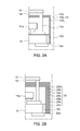
- FIG. 2A illustrates an enlarged view of an area ‘A’ denoted by dotted line in FIG. 1B , in accordance with an embodiment of the present disclosure.
- the EMI shield 13 in this embodiment includes a non-magnetic (or weakly magnetic) conductive layer 13 a , an insulating layer 13 b , and a magnetic conductive layer 13 c .
- the insulating layer 13 b is located between the non-magnetic conductive layer 13 a and the magnetic conductive layer 13 c .
- An interconnection 13 d is used to electrically connect the non-magnetic conductive layer 13 a and the magnetic conductive layer 13 c.
- the non-magnetic conductive layer 13 a is, or includes, a material with a high conductivity.
- the non-magnetic conductive layer 13 a is Ag, Cu, Al, Au, or an alloy thereof.
- the insulating layer 13 b is insulating, and can be magnetic or non-magnetic.
- the insulating layer 13 b can be, or can include, for example, ferromagnetic materials such as barium ferrate or strontium ferrite.
- the insulating layer 13 b can be, or can include, an oxidized form of metals or non-metals such as silicon dioxide (SiO 2 ) or aluminum oxide (Al 2 O 3 ).
- the magnetic conductive layer 13 c can be, or can include, for example, molybdenum (Mo), nickel (Ni), cobalt (Co), iron (Fe), or an alloy thereof.
- the non-magnetic conductive layer 13 a can be used to resist high frequency (e.g., greater than about 1 GHz) electromagnetic radiation.
- the resistance to high frequency electromagnetic radiation is related to mechanisms of absorption and reflection within the non-magnetic conductive layer 13 a .
- the effectiveness of absorption is directly proportional to the product ( ⁇ r) ⁇ ( ⁇ r), where ( ⁇ r) is the electrical conductivity relative to copper and ( ⁇ r) is the magnetic permeability relative to copper.
- the effectiveness of reflection is directly proportional to the ratio ( ⁇ r)/( ⁇ r).
- the non-magnetic conductive layer 13 a and the insulating layer 13 b can be used to resist low frequency (e.g., less than about 1 GHz) electromagnetic radiation. Resistance to low frequency electromagnetic radiation is related to mechanisms of absorption within the non-magnetic conductive layer 13 a , as well as a magnetic field induced by eddy currents within the EMI shield 13 . The effectiveness of absorption is directly proportional to the product ( ⁇ r) ⁇ ( ⁇ r). An external magnetic field induces eddy currents, which can generate a reverse magnetic field to resist low frequency external electromagnetic radiation.
- low frequency electromagnetic radiation e.g., less than about 1 GHz
- Resistance to low frequency electromagnetic radiation is related to mechanisms of absorption within the non-magnetic conductive layer 13 a , as well as a magnetic field induced by eddy currents within the EMI shield 13 .
- the effectiveness of absorption is directly proportional to the product ( ⁇ r) ⁇ ( ⁇ r).
- An external magnetic field induces eddy currents, which can
- the insulating layer 13 b between the non-magnetic conductive layer 13 a and the magnetic conductive layer 13 c , two eddy currents will be generated; one at an interface of the non-magnetic conductive layer 13 a and the insulating layer 13 b , and one at an interface of the magnetic conductive layer 13 c and the insulating layer 13 b.
- the EMI shield 13 illustrated in FIG. 2A provides for improved electromagnetic shielding against both higher frequency electromagnetic radiation and lower frequency electromagnetic radiation, in comparison with a conventional EMI shield with single layer of thickness approximately equal to a thickness of the EMI shield 13 of FIG. 2A .
- the EMI shield 13 can include additional conductive layers with insulating layers interposed between, providing additional interfaces with eddy currents, so that the EMI shield 13 can provide better shielding effectiveness with respect to lower frequency electromagnetic radiation.
- thinner layers may be used throughout the EMI shield 13 , so that additional layers may be included without increasing the total thickness of the EMI shield 13 .
- MIM metal-insulator-metal
- the interconnection 13 d is selectively connected to each conductive layer of EMI shield 13 and is further electrically coupled to a ground pad to discharge the positive charges accumulated on exterior conductive layers and reduce or eliminate the leakage current.
- FIG. 2B illustrates an enlarged view of the area ‘A’ denoted by dotted line in FIG. 1B , in accordance with another embodiment of the present disclosure.
- the EMI shield 13 of FIG. 1B is denoted for the embodiment of FIG. 2B as an EMI shield 23 with two non-magnetic conductive layers 23 a , three insulating layers 23 b , and two magnetic conductive layers 23 c . As shown in FIG. 2B , there is one insulating layer 23 b located between each non-magnetic conductive layer 23 a and magnetic conductive layer 23 c pair.
- each non-magnetic conductive layer 23 a is separated from a neighboring magnetic conductive layer 23 c by an insulating layer 23 b , such that each non-magnetic conductive layer 23 a is separated from each magnetic conductive layer 23 c .
- multiple insulating layers 23 b can be positioned between a non-magnetic conductive layer 23 a and a neighboring magnetic conductive layer 23 c .
- An interconnection 23 d is used to electrically connect ones of the non-magnetic conductive layers 23 a to ones of the magnetic conductive layers 23 c.
- the EMI shield 23 will generate more eddy currents.
- a stronger reverse magnetic field will be induced to resist the original magnetic field which resulted in the eddy currents being generated. Therefore, in comparison with the EMI shield 13 shown in FIG. 2A , the EMI shield 23 shown in FIG. 2B provides improved electromagnetic shielding capabilities.
- the number of non-magnetic conductive layers 23 a , insulating layers 23 b and magnetic conductive layers 23 c can be determined based on design specifications. Note that the EMI shields 13 , 23 block magnetic fields generated internally or externally to the semiconductor device package 1 .
- FIGS. 3A-3D illustrate a semiconductor manufacturing process in accordance with an embodiment of the present disclosure.
- a substrate 10 is provided.
- the substrate 10 is, for example, a printed circuit board, such as a paper-based copper foil laminate, a composite copper foil laminate, or a polymer-impregnated glass-fiber-based copper foil laminate.
- the substrate 10 can include a redistribution layer (RDL) or traces for electrical connection between components mounted on a top surface 101 of the substrate 10 .
- the substrate 10 includes through vias penetrating the substrate 10 , within which are formed electrical connections 10 c between the components mounted on the top surface 101 and components mounted on the bottom surface 103 of the substrate 10 .
- the substrate 10 can be replaced by other suitable carriers, such as a leadframe.
- Electronic components 11 a , 11 b and conductive elements 15 c are placed on the top surface 101 of the substrate 10 .
- electronic components 11 a , 11 b can be placed on pads 10 p on the top surface 101 of the substrate 10 .
- the conductive elements 15 c electrically connect to electronic components such as the electronic component 11 a.
- a package body 12 is formed to substantially cover or encapsulate the electronic components 11 a , 11 b and the conductive element 15 c .
- the package body 12 can be formed by applying an encapsulant to the top surface 101 of the substrate 10 .
- the encapsulant can include, for example, a Novolac-based resin, an epoxy-based resin, a silicone-based resin, or another suitable material.
- the encapsulant can be applied using any of a number of molding techniques, such as compression molding, injection molding, or transfer molding.
- An EMI shield 13 is formed to cover a top surface 121 and a lateral surface or surfaces 122 of the package body 12 , and to cover a lateral surface or surfaces 102 of the substrate 10 .
- the EMI shield 13 can be formed using any of a number of coating techniques, such as electroless plating, electroplating, printing, spraying, sputtering, or vacuum deposition.
- the EMI shield 13 is multi-layered, and includes a non-magnetic conductive layer 13 a , an insulating layer 13 b and a magnetic conductive layer 13 c , such as shown in FIG. 2A .
- Different layers of the EMI shield 13 can be formed using the same or similar coating technique, or different coating techniques.
- the EMI shield 13 includes multiple non-magnetic conductive layers 23 a , multiple insulating layers 23 b and multiple magnetic conductive layers 23 c , as shown in FIG. 2B .
- holes 13 h are formed through the EMI shield 13 at a top surface 131 of the EMI shield 13 , to expose a top portion of the conductive element 15 c .
- the holes 13 h can be formed by, for example, laser drilling or etching technology.
- a magnetic insulating layer 14 is formed on the top surface 131 of the EMI shield 13 , and a patterned conductive layer 15 is formed on a top surface 141 of the magnetic insulating layer 14 .
- the magnetic insulating layer 14 can be formed by, for example, 3D printing or sputtering.
- the patterned conductive layer 15 can be formed by, for example, 3D printing, evaporating, sputtering or electroplating.
- the patterned conductive layer 15 is formed as a coil structure of planar coils with one or more layers of turns. In one or more embodiments, the coil structure is preformed, and attached to the magnetic insulating layer 14 .
- a conductive element 15 w is formed to electrically connect the patterned conductive layer 15 to a portion of the conductive element 15 c exposed in the hole 13 h .
- the conductive element 15 w is a bonding wire.
- An insulation material 15 p is formed to cover and protect the conductive element 15 w .
- the conductive element 15 w is a conductive stud or a conductive pillar.
- FIGS. 4A-4D illustrate a semiconductor manufacturing process in accordance with an embodiment of the present disclosure.
- FIG. 4A The manufacturing operations shown in FIG. 4A are similar to those shown in FIG. 3A , except that in FIG. 4A , a first portion 421 of a package body 42 encapsulating the conductive element 15 c is higher than a second portion 422 of the package body 42 encapsulating the electronic components 11 a , 11 b .
- the package body 42 can be formed, for example, using an irregular molding process or a selective molding process.
- An EMI shield 43 is formed on the package body 42 , including a first portion 431 over the first portion 421 of the package body 42 , and a second portion 432 over the second portion 422 of the package body 42 .
- the EMI shield 43 is further formed on the conductive element 15 c.
- the first portion 421 of the package body 42 and the first portion 431 of the EMI shield 43 are removed to expose a top portion of the conductive element 15 c .
- the exposed portion of the conductive element 15 c is substantially coplanar with a top surface of the second portion 432 of the EMI shield 43 , as shown in FIG. 4B .
- the exposed portion of the conductive element 15 c along with some of the first portion 431 of the shield 43 , extends above the top surface of the second portion 432 of the EMI shield 43 .
- the first portion 421 of the package body 42 and the first portion 431 of the EMI shield 43 can be removed by, for example, cutting, laser or etching technology.
- a magnetic insulating layer 14 is formed on the second portion 432 of the EMI shield 43 above the second portion 422 of the package body 42 .
- the magnetic insulating layer 14 can be formed by, for example, 3D printing or sputtering.
- a patterned conductive layer 15 is formed on a top surface 141 of the magnetic insulating layer 14 and contacts the conductive element 15 c to form an electrical connection.
- the patterned conductive layer 15 can be formed by, for example, 3D printing, evaporating, sputtering or electroplating.
- the patterned conductive layer 15 is formed as a coil structure of planar coils with one or more layers of turns.
- the patterned conductive layer 15 electrically contacts the exposed portion of the conductive element 15 c and is isolated from the EMI shield 43 .
- the terms “substantially” and “about” are used to describe and account for small variations.
- the terms can refer to less than or equal to ⁇ 10%, such as less than or equal to ⁇ 5%, less than or equal to ⁇ 4%, less than or equal to ⁇ 3%, less than or equal to ⁇ 2%, less than or equal to ⁇ 1%, less than or equal to ⁇ 0.5%, less than or equal to ⁇ 0.1%, or less than or equal to ⁇ 0.05%.
- two surfaces can be deemed to be coplanar or substantially coplanar if a displacement between the two surfaces is no greater than 5 ⁇ m, no greater than 2 ⁇ m, no greater than 1 ⁇ m, or no greater than 0.5 ⁇ m.
- a material can be deemed to “substantially cover” a surface if the material covers greater than 95% of the surface; and a material can be deemed to “substantially cover” a component if more than 95% of each surface of the component exposed to the material is covered by the material.
Landscapes
- Engineering & Computer Science (AREA)
- Power Engineering (AREA)
- Physics & Mathematics (AREA)
- Microelectronics & Electronic Packaging (AREA)
- Computer Hardware Design (AREA)
- General Physics & Mathematics (AREA)
- Condensed Matter Physics & Semiconductors (AREA)
- Manufacturing & Machinery (AREA)
- Ceramic Engineering (AREA)
- Computer Networks & Wireless Communication (AREA)
- Geometry (AREA)
- Health & Medical Sciences (AREA)
- Electromagnetism (AREA)
- Toxicology (AREA)
- Shielding Devices Or Components To Electric Or Magnetic Fields (AREA)
Abstract
Description
Claims (8)
Priority Applications (2)
| Application Number | Priority Date | Filing Date | Title |
|---|---|---|---|
| US14/805,847 US9461001B1 (en) | 2015-07-22 | 2015-07-22 | Semiconductor device package integrated with coil for wireless charging and electromagnetic interference shielding, and method of manufacturing the same |
| US15/257,723 US9922938B2 (en) | 2015-07-22 | 2016-09-06 | Semiconductor device package integrated with coil for wireless charging and electromagnetic interference shielding, and method of manufacturing the same |
Applications Claiming Priority (1)
| Application Number | Priority Date | Filing Date | Title |
|---|---|---|---|
| US14/805,847 US9461001B1 (en) | 2015-07-22 | 2015-07-22 | Semiconductor device package integrated with coil for wireless charging and electromagnetic interference shielding, and method of manufacturing the same |
Related Child Applications (1)
| Application Number | Title | Priority Date | Filing Date |
|---|---|---|---|
| US15/257,723 Continuation US9922938B2 (en) | 2015-07-22 | 2016-09-06 | Semiconductor device package integrated with coil for wireless charging and electromagnetic interference shielding, and method of manufacturing the same |
Publications (1)
| Publication Number | Publication Date |
|---|---|
| US9461001B1 true US9461001B1 (en) | 2016-10-04 |
Family
ID=56995151
Family Applications (2)
| Application Number | Title | Priority Date | Filing Date |
|---|---|---|---|
| US14/805,847 Active US9461001B1 (en) | 2015-07-22 | 2015-07-22 | Semiconductor device package integrated with coil for wireless charging and electromagnetic interference shielding, and method of manufacturing the same |
| US15/257,723 Active US9922938B2 (en) | 2015-07-22 | 2016-09-06 | Semiconductor device package integrated with coil for wireless charging and electromagnetic interference shielding, and method of manufacturing the same |
Family Applications After (1)
| Application Number | Title | Priority Date | Filing Date |
|---|---|---|---|
| US15/257,723 Active US9922938B2 (en) | 2015-07-22 | 2016-09-06 | Semiconductor device package integrated with coil for wireless charging and electromagnetic interference shielding, and method of manufacturing the same |
Country Status (1)
| Country | Link |
|---|---|
| US (2) | US9461001B1 (en) |
Cited By (64)
| Publication number | Priority date | Publication date | Assignee | Title |
|---|---|---|---|---|
| US20160126196A1 (en) | 2014-11-03 | 2016-05-05 | Rf Micro Devices, Inc. | Printed circuit module having a semiconductor device with a protective layer in place of a low-resistivity handle layer |
| US20170110413A1 (en) * | 2015-10-20 | 2017-04-20 | Taiwan Semiconductor Manufacturing Company, Ltd. | Wafer level shielding in multi-stacked fan out packages and methods of forming same |
| US20170170676A1 (en) * | 2015-12-09 | 2017-06-15 | Intel Corporation | Foldable fabric-based packaging solution |
| US20170295643A1 (en) * | 2016-04-12 | 2017-10-12 | Tdk Corporation | Electronic circuit module and manufacturing method of the same |
| US20170301628A1 (en) * | 2016-03-23 | 2017-10-19 | Tdk Corporation | Electronic circuit package |
| US9812350B2 (en) | 2013-03-06 | 2017-11-07 | Qorvo Us, Inc. | Method of manufacture for a silicon-on-plastic semiconductor device with interfacial adhesion layer |
| US9824951B2 (en) | 2014-09-12 | 2017-11-21 | Qorvo Us, Inc. | Printed circuit module having semiconductor device with a polymer substrate and methods of manufacturing the same |
| US20170358511A1 (en) | 2016-06-10 | 2017-12-14 | Qorvo Us, Inc. | Thermally enhanced semiconductor package with thermal additive and process for making the same |
| US20180019184A1 (en) | 2016-07-18 | 2018-01-18 | Qorvo Us, Inc. | Thermally enhanced semiconductor package having field effect transistors with back-gate feature |
| US20180044177A1 (en) | 2016-08-12 | 2018-02-15 | Qorvo Us, Inc. | Wafer-level package with enhanced performance |
| US9960145B2 (en) | 2015-03-25 | 2018-05-01 | Qorvo Us, Inc. | Flip chip module with enhanced properties |
| US10020405B2 (en) | 2016-01-19 | 2018-07-10 | Qorvo Us, Inc. | Microelectronics package with integrated sensors |
| US10020206B2 (en) | 2015-03-25 | 2018-07-10 | Qorvo Us, Inc. | Encapsulated dies with enhanced thermal performance |
| US10038055B2 (en) | 2015-05-22 | 2018-07-31 | Qorvo Us, Inc. | Substrate structure with embedded layer for post-processing silicon handle elimination |
| US20180228030A1 (en) | 2014-10-01 | 2018-08-09 | Qorvo Us, Inc. | Method for manufacturing an integrated circuit package |
| US10062637B2 (en) | 2013-10-31 | 2018-08-28 | Qorvo Us, Inc. | Method of manufacture for a semiconductor device |
| US10062583B2 (en) | 2016-05-09 | 2018-08-28 | Qorvo Us, Inc. | Microelectronics package with inductive element and magnetically enhanced mold compound component |
| US10068831B2 (en) | 2016-12-09 | 2018-09-04 | Qorvo Us, Inc. | Thermally enhanced semiconductor package and process for making the same |
| US10074622B2 (en) * | 2017-02-06 | 2018-09-11 | Advanced Semiconductor Engineering, Inc. | Semiconductor package device and method of manufacturing the same |
| US10090339B2 (en) | 2016-10-21 | 2018-10-02 | Qorvo Us, Inc. | Radio frequency (RF) switch |
| CN108630624A (en) * | 2017-03-24 | 2018-10-09 | 艾马克科技公司 | Electronic device and manufacturing method thereof |
| US10109502B2 (en) | 2016-09-12 | 2018-10-23 | Qorvo Us, Inc. | Semiconductor package with reduced parasitic coupling effects and process for making the same |
| US10109550B2 (en) | 2016-08-12 | 2018-10-23 | Qorvo Us, Inc. | Wafer-level package with enhanced performance |
| US20190013255A1 (en) | 2017-07-06 | 2019-01-10 | Qorvo Us, Inc. | Wafer-level packaging for enhanced performance |
| US20190074263A1 (en) | 2017-09-05 | 2019-03-07 | Qorvo Us, Inc. | Microelectronics package with self-aligned stacked-die assembly |
| US20190074271A1 (en) | 2017-09-05 | 2019-03-07 | Qorvo Us, Inc. | Microelectronics package with self-aligned stacked-die assembly |
| US10276495B2 (en) | 2015-09-11 | 2019-04-30 | Qorvo Us, Inc. | Backside semiconductor die trimming |
| US10373917B2 (en) * | 2017-12-05 | 2019-08-06 | Tdk Corporation | Electronic circuit package using conductive sealing material |
| US10411766B2 (en) | 2017-03-14 | 2019-09-10 | Advanced Semiconductor Engineering, Inc. | Semiconductor package device and method of manufacturing the same |
| US10431554B2 (en) | 2016-01-07 | 2019-10-01 | Advanced Semiconductor Engineering, Inc. | Semiconductor device package and method of manufacturing the same |
| US10486963B2 (en) | 2016-08-12 | 2019-11-26 | Qorvo Us, Inc. | Wafer-level package with enhanced performance |
| US20200161252A1 (en) * | 2018-11-16 | 2020-05-21 | STATS ChipPAC Pte. Ltd. | Molded Laser Package with Electromagnetic Interference Shield and Method of Making |
| US20200235054A1 (en) | 2019-01-23 | 2020-07-23 | Qorvo Us, Inc. | Rf devices with enhanced performance and methods of forming the same |
| US10749518B2 (en) | 2016-11-18 | 2020-08-18 | Qorvo Us, Inc. | Stacked field-effect transistor switch |
| US10773952B2 (en) | 2016-05-20 | 2020-09-15 | Qorvo Us, Inc. | Wafer-level package with enhanced performance |
| US10784149B2 (en) | 2016-05-20 | 2020-09-22 | Qorvo Us, Inc. | Air-cavity module with enhanced device isolation |
| CN111739876A (en) * | 2020-05-20 | 2020-10-02 | 甬矽电子(宁波)股份有限公司 | Packaged antenna structure, method of making the same, and electronic device |
| US10804246B2 (en) | 2018-06-11 | 2020-10-13 | Qorvo Us, Inc. | Microelectronics package with vertically stacked dies |
| EP3560111A4 (en) * | 2016-12-21 | 2020-12-02 | Intel Capital Corporation | WIRELESS COMMUNICATION TECHNOLOGY, DEVICES, AND PROCEDURES |
| US10964554B2 (en) | 2018-10-10 | 2021-03-30 | Qorvo Us, Inc. | Wafer-level fan-out package with enhanced performance |
| CN112713140A (en) * | 2019-10-25 | 2021-04-27 | 中芯长电半导体(江阴)有限公司 | Antenna packaging structure and packaging method |
| US11069590B2 (en) | 2018-10-10 | 2021-07-20 | Qorvo Us, Inc. | Wafer-level fan-out package with enhanced performance |
| US20210296199A1 (en) | 2018-11-29 | 2021-09-23 | Qorvo Us, Inc. | Thermally enhanced semiconductor package with at least one heat extractor and process for making the same |
| US11152363B2 (en) | 2018-03-28 | 2021-10-19 | Qorvo Us, Inc. | Bulk CMOS devices with enhanced performance and methods of forming the same utilizing bulk CMOS process |
| US11255014B2 (en) * | 2018-10-01 | 2022-02-22 | Tetos Co., Ltd. | Apparatus for depositing metal film on surface of three-dimensional object |
| US20220066036A1 (en) * | 2020-08-25 | 2022-03-03 | Lumentum Operations Llc | Package for a time of flight device |
| US20220108938A1 (en) | 2019-01-23 | 2022-04-07 | Qorvo Us, Inc. | Rf devices with enhanced performance and methods of forming the same |
| US20220139862A1 (en) | 2019-01-23 | 2022-05-05 | Qorvo Us, Inc. | Rf devices with enhanced performance and methods of forming the same |
| US11387157B2 (en) | 2019-01-23 | 2022-07-12 | Qorvo Us, Inc. | RF devices with enhanced performance and methods of forming the same |
| US11437295B2 (en) * | 2017-08-16 | 2022-09-06 | Samsung Electro-Mechanics Co., Ltd. | Semiconductor package and electronic device having the same |
| US11646289B2 (en) | 2019-12-02 | 2023-05-09 | Qorvo Us, Inc. | RF devices with enhanced performance and methods of forming the same |
| US11923238B2 (en) | 2019-12-12 | 2024-03-05 | Qorvo Us, Inc. | Method of forming RF devices with enhanced performance including attaching a wafer to a support carrier by a bonding technique without any polymer adhesive |
| US12046483B2 (en) | 2019-01-23 | 2024-07-23 | Qorvo Us, Inc. | RF devices with enhanced performance and methods of forming the same |
| US12046535B2 (en) | 2018-07-02 | 2024-07-23 | Qorvo Us, Inc. | RF devices with enhanced performance and methods of forming the same |
| US12046505B2 (en) | 2018-04-20 | 2024-07-23 | Qorvo Us, Inc. | RF devices with enhanced performance and methods of forming the same utilizing localized SOI formation |
| US12062571B2 (en) | 2021-03-05 | 2024-08-13 | Qorvo Us, Inc. | Selective etching process for SiGe and doped epitaxial silicon |
| US12062700B2 (en) | 2018-04-04 | 2024-08-13 | Qorvo Us, Inc. | Gallium-nitride-based module with enhanced electrical performance and process for making the same |
| US20240270081A1 (en) * | 2022-05-31 | 2024-08-15 | Rolls-Royce Deutschland Ltd & Co Kg | High voltage power converter |
| US12074086B2 (en) | 2019-11-01 | 2024-08-27 | Qorvo Us, Inc. | RF devices with nanotube particles for enhanced performance and methods of forming the same |
| US20240290728A1 (en) * | 2023-02-24 | 2024-08-29 | Siliconware Precision Industries Co., Ltd. | Electronic package and manufacturing method thereof |
| US12125825B2 (en) | 2019-01-23 | 2024-10-22 | Qorvo Us, Inc. | RF devices with enhanced performance and methods of forming the same |
| US12129168B2 (en) | 2019-12-23 | 2024-10-29 | Qorvo Us, Inc. | Microelectronics package with vertically stacked MEMS device and controller device |
| US12402245B2 (en) * | 2020-11-02 | 2025-08-26 | Murata Manufacturing Co., Ltd. | Radio-frequency module and communication device |
| US12482731B2 (en) | 2020-12-11 | 2025-11-25 | Qorvo Us, Inc. | Multi-level 3D stacked package and methods of forming the same |
Families Citing this family (12)
| Publication number | Priority date | Publication date | Assignee | Title |
|---|---|---|---|---|
| US20170214269A1 (en) * | 2016-01-22 | 2017-07-27 | Boston Scientific Neuromodulation Corporation | Physically-Configurable External Charger for an Implantable Medical Device with Receptacle in Coil Housing for Electronics Module |
| US10135335B2 (en) * | 2016-08-22 | 2018-11-20 | Infineon Technologies Americas Corp. | Powerstage attached to inductor |
| FR3061999B1 (en) * | 2017-01-19 | 2019-08-23 | Institut Vedecom | WIRELESS CHARGING PANEL, EQUIPPED ENERGY STORAGE UNIT AND CHARGEABLE POWER SUPPLY SYSTEM |
| US10211794B1 (en) * | 2017-12-04 | 2019-02-19 | Nxp Usa, Inc. | Silicon shielding for baseband termination and RF performance enhancement |
| CN108422875A (en) * | 2018-02-07 | 2018-08-21 | 内蒙古聚能节能服务有限公司 | A kind of packaged type charging small handcart |
| DE102018205670A1 (en) * | 2018-04-13 | 2019-10-17 | Fraunhofer-Gesellschaft zur Förderung der angewandten Forschung e.V. | Hermetically sealed module unit with integrated antennas |
| MY200763A (en) * | 2018-07-23 | 2024-01-14 | Intel Corp | Extended package air core inductor |
| US11038267B2 (en) * | 2018-07-31 | 2021-06-15 | Skyworks Solutions, Inc. | Apparatus and methods for electromagnetic shielding using an outer cobalt layer |
| JP6905493B2 (en) * | 2018-08-24 | 2021-07-21 | 株式会社東芝 | Electronic device |
| US11296043B2 (en) * | 2019-12-04 | 2022-04-05 | Advanced Semiconductor Engineering, Inc. | Semiconductor device packages and methods of manufacturing the same |
| US11437306B2 (en) | 2020-02-04 | 2022-09-06 | Stmicroelectronics (Grenoble 2) Sas | Electronics unit with integrated metallic pattern |
| EP4481812A1 (en) * | 2023-06-20 | 2024-12-25 | Infineon Technologies AG | Radio frequency semiconductor device and method for fabricating a radio frequency semiconductor device |
Citations (8)
| Publication number | Priority date | Publication date | Assignee | Title |
|---|---|---|---|---|
| US5639989A (en) | 1994-04-19 | 1997-06-17 | Motorola Inc. | Shielded electronic component assembly and method for making the same |
| US20040217472A1 (en) * | 2001-02-16 | 2004-11-04 | Integral Technologies, Inc. | Low cost chip carrier with integrated antenna, heat sink, or EMI shielding functions manufactured from conductive loaded resin-based materials |
| US8058714B2 (en) * | 2008-09-25 | 2011-11-15 | Skyworks Solutions, Inc. | Overmolded semiconductor package with an integrated antenna |
| US8399964B2 (en) * | 2006-06-02 | 2013-03-19 | Honeywell International Inc. | Multilayer structures for magnetic shielding |
| US20140140001A1 (en) * | 2012-11-20 | 2014-05-22 | International Business Machines Corporation | Variable thickness emi shield with variable cooling channel size |
| US8786060B2 (en) | 2012-05-04 | 2014-07-22 | Advanced Semiconductor Engineering, Inc. | Semiconductor package integrated with conformal shield and antenna |
| US20140231973A1 (en) * | 2012-04-26 | 2014-08-21 | Dacheng Huang | Semiconductor device including electromagnetic absorption and shielding |
| US9153543B1 (en) * | 2012-01-23 | 2015-10-06 | Amkor Technology, Inc. | Shielding technique for semiconductor package including metal lid and metalized contact area |
Family Cites Families (35)
| Publication number | Priority date | Publication date | Assignee | Title |
|---|---|---|---|---|
| US7633170B2 (en) | 2005-01-05 | 2009-12-15 | Advanced Semiconductor Engineering, Inc. | Semiconductor device package and manufacturing method thereof |
| US7656047B2 (en) | 2005-01-05 | 2010-02-02 | Advanced Semiconductor Engineering, Inc. | Semiconductor device package and manufacturing method |
| US20060208347A1 (en) * | 2005-03-17 | 2006-09-21 | Kim Kidon | Semiconductor device package |
| TWI376774B (en) * | 2007-06-08 | 2012-11-11 | Cyntec Co Ltd | Three dimensional package structure |
| US8212339B2 (en) | 2008-02-05 | 2012-07-03 | Advanced Semiconductor Engineering, Inc. | Semiconductor device packages with electromagnetic interference shielding |
| US7989928B2 (en) | 2008-02-05 | 2011-08-02 | Advanced Semiconductor Engineering Inc. | Semiconductor device packages with electromagnetic interference shielding |
| US8350367B2 (en) | 2008-02-05 | 2013-01-08 | Advanced Semiconductor Engineering, Inc. | Semiconductor device packages with electromagnetic interference shielding |
| US8022511B2 (en) | 2008-02-05 | 2011-09-20 | Advanced Semiconductor Engineering, Inc. | Semiconductor device packages with electromagnetic interference shielding |
| US7829981B2 (en) | 2008-07-21 | 2010-11-09 | Advanced Semiconductor Engineering, Inc. | Semiconductor device packages with electromagnetic interference shielding |
| US8410584B2 (en) * | 2008-08-08 | 2013-04-02 | Advanced Semiconductor Engineering, Inc. | Semiconductor device packages with electromagnetic interference shielding |
| US20100110656A1 (en) | 2008-10-31 | 2010-05-06 | Advanced Semiconductor Engineering, Inc. | Chip package and manufacturing method thereof |
| US8212340B2 (en) | 2009-07-13 | 2012-07-03 | Advanced Semiconductor Engineering, Inc. | Chip package and manufacturing method thereof |
| TWI436470B (en) * | 2009-09-30 | 2014-05-01 | 日月光半導體製造股份有限公司 | Packaging process and package structure |
| US8030750B2 (en) | 2009-11-19 | 2011-10-04 | Advanced Semiconductor Engineering, Inc. | Semiconductor device packages with electromagnetic interference shielding |
| US8378466B2 (en) | 2009-11-19 | 2013-02-19 | Advanced Semiconductor Engineering, Inc. | Wafer-level semiconductor device packages with electromagnetic interference shielding |
| US8368185B2 (en) | 2009-11-19 | 2013-02-05 | Advanced Semiconductor Engineering, Inc. | Semiconductor device packages with electromagnetic interference shielding |
| US8946886B1 (en) * | 2010-05-13 | 2015-02-03 | Amkor Technology, Inc. | Shielded electronic component package and method |
| US9007273B2 (en) | 2010-09-09 | 2015-04-14 | Advances Semiconductor Engineering, Inc. | Semiconductor package integrated with conformal shield and antenna |
| US8642119B2 (en) * | 2010-09-22 | 2014-02-04 | Stmicroelectronics Pte Ltd. | Method and system for shielding semiconductor devices from light |
| US8704341B2 (en) * | 2012-05-15 | 2014-04-22 | Advanced Semiconductor Engineering, Inc. | Semiconductor packages with thermal dissipation structures and EMI shielding |
| US9153542B2 (en) | 2012-08-01 | 2015-10-06 | Advanced Semiconductor Engineering, Inc. | Semiconductor package having an antenna and manufacturing method thereof |
| US9484313B2 (en) | 2013-02-27 | 2016-11-01 | Advanced Semiconductor Engineering, Inc. | Semiconductor packages with thermal-enhanced conformal shielding and related methods |
| US9129954B2 (en) | 2013-03-07 | 2015-09-08 | Advanced Semiconductor Engineering, Inc. | Semiconductor package including antenna layer and manufacturing method thereof |
| CN103400825B (en) | 2013-07-31 | 2016-05-18 | 日月光半导体制造股份有限公司 | Semiconductor package and manufacturing method thereof |
| CN105226045B (en) | 2014-05-30 | 2018-07-27 | 日月光半导体制造股份有限公司 | Semiconductor device and method for manufacturing the same |
| TWI540652B (en) | 2014-07-30 | 2016-07-01 | 日月光半導體製造股份有限公司 | Electronic package module and manufacturing method thereof |
| US9269673B1 (en) | 2014-10-22 | 2016-02-23 | Advanced Semiconductor Engineering, Inc. | Semiconductor device packages |
| US9190367B1 (en) | 2014-10-22 | 2015-11-17 | Advanced Semiconductor Engineering, Inc. | Semiconductor package structure and semiconductor process |
| US9484307B2 (en) | 2015-01-26 | 2016-11-01 | Advanced Semiconductor Engineering, Inc. | Fan-out wafer level packaging structure |
| US9653415B2 (en) | 2015-02-18 | 2017-05-16 | Advanced Semiconductor Engineering, Inc. | Semiconductor device packages and method of making the same |
| US9589906B2 (en) | 2015-02-27 | 2017-03-07 | Advanced Semiconductor Engineering, Inc. | Semiconductor device package and method of manufacturing the same |
| US9437576B1 (en) | 2015-03-23 | 2016-09-06 | Advanced Semiconductor Engineering, Inc. | Semiconductor device package and method of manufacturing the same |
| US9589871B2 (en) | 2015-04-13 | 2017-03-07 | Advanced Semiconductor Engineering, Inc. | Semiconductor package structure and method for manufacturing the same |
| CN106299598B (en) * | 2015-05-27 | 2020-08-21 | 富泰华工业(深圳)有限公司 | Electronic device and its multi-feed antenna |
| US9653407B2 (en) | 2015-07-02 | 2017-05-16 | Advanced Semiconductor Engineering, Inc. | Semiconductor device packages |
-
2015
- 2015-07-22 US US14/805,847 patent/US9461001B1/en active Active
-
2016
- 2016-09-06 US US15/257,723 patent/US9922938B2/en active Active
Patent Citations (8)
| Publication number | Priority date | Publication date | Assignee | Title |
|---|---|---|---|---|
| US5639989A (en) | 1994-04-19 | 1997-06-17 | Motorola Inc. | Shielded electronic component assembly and method for making the same |
| US20040217472A1 (en) * | 2001-02-16 | 2004-11-04 | Integral Technologies, Inc. | Low cost chip carrier with integrated antenna, heat sink, or EMI shielding functions manufactured from conductive loaded resin-based materials |
| US8399964B2 (en) * | 2006-06-02 | 2013-03-19 | Honeywell International Inc. | Multilayer structures for magnetic shielding |
| US8058714B2 (en) * | 2008-09-25 | 2011-11-15 | Skyworks Solutions, Inc. | Overmolded semiconductor package with an integrated antenna |
| US9153543B1 (en) * | 2012-01-23 | 2015-10-06 | Amkor Technology, Inc. | Shielding technique for semiconductor package including metal lid and metalized contact area |
| US20140231973A1 (en) * | 2012-04-26 | 2014-08-21 | Dacheng Huang | Semiconductor device including electromagnetic absorption and shielding |
| US8786060B2 (en) | 2012-05-04 | 2014-07-22 | Advanced Semiconductor Engineering, Inc. | Semiconductor package integrated with conformal shield and antenna |
| US20140140001A1 (en) * | 2012-11-20 | 2014-05-22 | International Business Machines Corporation | Variable thickness emi shield with variable cooling channel size |
Cited By (115)
| Publication number | Priority date | Publication date | Assignee | Title |
|---|---|---|---|---|
| US10134627B2 (en) | 2013-03-06 | 2018-11-20 | Qorvo Us, Inc. | Silicon-on-plastic semiconductor device with interfacial adhesion layer |
| US9812350B2 (en) | 2013-03-06 | 2017-11-07 | Qorvo Us, Inc. | Method of manufacture for a silicon-on-plastic semiconductor device with interfacial adhesion layer |
| US10062637B2 (en) | 2013-10-31 | 2018-08-28 | Qorvo Us, Inc. | Method of manufacture for a semiconductor device |
| US9824951B2 (en) | 2014-09-12 | 2017-11-21 | Qorvo Us, Inc. | Printed circuit module having semiconductor device with a polymer substrate and methods of manufacturing the same |
| US20180228030A1 (en) | 2014-10-01 | 2018-08-09 | Qorvo Us, Inc. | Method for manufacturing an integrated circuit package |
| US10492301B2 (en) | 2014-10-01 | 2019-11-26 | Qorvo Us, Inc. | Method for manufacturing an integrated circuit package |
| US10085352B2 (en) | 2014-10-01 | 2018-09-25 | Qorvo Us, Inc. | Method for manufacturing an integrated circuit package |
| US20160126196A1 (en) | 2014-11-03 | 2016-05-05 | Rf Micro Devices, Inc. | Printed circuit module having a semiconductor device with a protective layer in place of a low-resistivity handle layer |
| US10199301B2 (en) | 2014-11-03 | 2019-02-05 | Qorvo Us, Inc. | Methods of manufacturing a printed circuit module having a semiconductor device with a protective layer in place of a low-resistivity handle layer |
| US10121718B2 (en) | 2014-11-03 | 2018-11-06 | Qorvo Us, Inc. | Printed circuit module having a semiconductor device with a protective layer in place of a low-resistivity handle layer |
| US10109548B2 (en) | 2014-11-03 | 2018-10-23 | Qorvo Us, Inc. | Printed circuit module having a semiconductor device with a protective layer in place of a low-resistivity handle layer |
| US9960145B2 (en) | 2015-03-25 | 2018-05-01 | Qorvo Us, Inc. | Flip chip module with enhanced properties |
| US10020206B2 (en) | 2015-03-25 | 2018-07-10 | Qorvo Us, Inc. | Encapsulated dies with enhanced thermal performance |
| US10038055B2 (en) | 2015-05-22 | 2018-07-31 | Qorvo Us, Inc. | Substrate structure with embedded layer for post-processing silicon handle elimination |
| US10276495B2 (en) | 2015-09-11 | 2019-04-30 | Qorvo Us, Inc. | Backside semiconductor die trimming |
| US9922939B2 (en) | 2015-10-20 | 2018-03-20 | Taiwan Semiconductor Manufacturing Company, Ltd. | Wafer level shielding in multi-stacked fan out packages and methods of forming same |
| US9659878B2 (en) * | 2015-10-20 | 2017-05-23 | Taiwan Semiconductor Manufacturing Company, Ltd. | Wafer level shielding in multi-stacked fan out packages and methods of forming same |
| US20170110413A1 (en) * | 2015-10-20 | 2017-04-20 | Taiwan Semiconductor Manufacturing Company, Ltd. | Wafer level shielding in multi-stacked fan out packages and methods of forming same |
| US10014710B2 (en) * | 2015-12-09 | 2018-07-03 | Intel Corporation | Foldable fabric-based packaging solution |
| US20170170676A1 (en) * | 2015-12-09 | 2017-06-15 | Intel Corporation | Foldable fabric-based packaging solution |
| US10431554B2 (en) | 2016-01-07 | 2019-10-01 | Advanced Semiconductor Engineering, Inc. | Semiconductor device package and method of manufacturing the same |
| US10020405B2 (en) | 2016-01-19 | 2018-07-10 | Qorvo Us, Inc. | Microelectronics package with integrated sensors |
| US9953932B2 (en) * | 2016-03-23 | 2018-04-24 | Tdk Corporation | Electronic circuit package |
| US20170301628A1 (en) * | 2016-03-23 | 2017-10-19 | Tdk Corporation | Electronic circuit package |
| US10225923B2 (en) * | 2016-04-12 | 2019-03-05 | Tdk Corporation | Electronic circuit module and manufacturing method of the same |
| US20170295643A1 (en) * | 2016-04-12 | 2017-10-12 | Tdk Corporation | Electronic circuit module and manufacturing method of the same |
| US10062583B2 (en) | 2016-05-09 | 2018-08-28 | Qorvo Us, Inc. | Microelectronics package with inductive element and magnetically enhanced mold compound component |
| US10090262B2 (en) * | 2016-05-09 | 2018-10-02 | Qorvo Us, Inc. | Microelectronics package with inductive element and magnetically enhanced mold compound component |
| US10882740B2 (en) | 2016-05-20 | 2021-01-05 | Qorvo Us, Inc. | Wafer-level package with enhanced performance and manufacturing method thereof |
| US10773952B2 (en) | 2016-05-20 | 2020-09-15 | Qorvo Us, Inc. | Wafer-level package with enhanced performance |
| US10784149B2 (en) | 2016-05-20 | 2020-09-22 | Qorvo Us, Inc. | Air-cavity module with enhanced device isolation |
| US10262915B2 (en) | 2016-06-10 | 2019-04-16 | Qorvo Us, Inc. | Thermally enhanced semiconductor package with thermal additive and process for making the same |
| US20170358511A1 (en) | 2016-06-10 | 2017-12-14 | Qorvo Us, Inc. | Thermally enhanced semiconductor package with thermal additive and process for making the same |
| US20180197803A1 (en) | 2016-06-10 | 2018-07-12 | Qorvo Us, Inc. | Thermally enhanced semiconductor package with thermal additive and process for making the same |
| US10103080B2 (en) | 2016-06-10 | 2018-10-16 | Qorvo Us, Inc. | Thermally enhanced semiconductor package with thermal additive and process for making the same |
| US10079196B2 (en) | 2016-07-18 | 2018-09-18 | Qorvo Us, Inc. | Thermally enhanced semiconductor package having field effect transistors with back-gate feature |
| US20180019184A1 (en) | 2016-07-18 | 2018-01-18 | Qorvo Us, Inc. | Thermally enhanced semiconductor package having field effect transistors with back-gate feature |
| US10468329B2 (en) | 2016-07-18 | 2019-11-05 | Qorvo Us, Inc. | Thermally enhanced semiconductor package having field effect transistors with back-gate feature |
| US10804179B2 (en) | 2016-08-12 | 2020-10-13 | Qorvo Us, Inc. | Wafer-level package with enhanced performance |
| US10109550B2 (en) | 2016-08-12 | 2018-10-23 | Qorvo Us, Inc. | Wafer-level package with enhanced performance |
| US10486965B2 (en) | 2016-08-12 | 2019-11-26 | Qorvo Us, Inc. | Wafer-level package with enhanced performance |
| US10486963B2 (en) | 2016-08-12 | 2019-11-26 | Qorvo Us, Inc. | Wafer-level package with enhanced performance |
| US20180044177A1 (en) | 2016-08-12 | 2018-02-15 | Qorvo Us, Inc. | Wafer-level package with enhanced performance |
| US10109502B2 (en) | 2016-09-12 | 2018-10-23 | Qorvo Us, Inc. | Semiconductor package with reduced parasitic coupling effects and process for making the same |
| US10985033B2 (en) | 2016-09-12 | 2021-04-20 | Qorvo Us, Inc. | Semiconductor package with reduced parasitic coupling effects and process for making the same |
| US10090339B2 (en) | 2016-10-21 | 2018-10-02 | Qorvo Us, Inc. | Radio frequency (RF) switch |
| US10749518B2 (en) | 2016-11-18 | 2020-08-18 | Qorvo Us, Inc. | Stacked field-effect transistor switch |
| US10068831B2 (en) | 2016-12-09 | 2018-09-04 | Qorvo Us, Inc. | Thermally enhanced semiconductor package and process for making the same |
| US10790216B2 (en) | 2016-12-09 | 2020-09-29 | Qorvo Us, Inc. | Thermally enhanced semiconductor package and process for making the same |
| US20180342439A1 (en) | 2016-12-09 | 2018-11-29 | Qorvo Us, Inc. | Thermally enhanced semiconductor package and process for making the same |
| EP3560111A4 (en) * | 2016-12-21 | 2020-12-02 | Intel Capital Corporation | WIRELESS COMMUNICATION TECHNOLOGY, DEVICES, AND PROCEDURES |
| US11424539B2 (en) | 2016-12-21 | 2022-08-23 | Intel Corporation | Wireless communication technology, apparatuses, and methods |
| US11955732B2 (en) | 2016-12-21 | 2024-04-09 | Intel Corporation | Wireless communication technology, apparatuses, and methods |
| US12237589B2 (en) | 2016-12-21 | 2025-02-25 | Intel Corporation | Wireless communication technology, apparatuses, and methods |
| US10332849B2 (en) | 2017-02-06 | 2019-06-25 | Advanced Semiconductor Engineering, Inc. | Semiconductor package device and method of manufacturing the same |
| US10074622B2 (en) * | 2017-02-06 | 2018-09-11 | Advanced Semiconductor Engineering, Inc. | Semiconductor package device and method of manufacturing the same |
| US10411766B2 (en) | 2017-03-14 | 2019-09-10 | Advanced Semiconductor Engineering, Inc. | Semiconductor package device and method of manufacturing the same |
| CN108630624A (en) * | 2017-03-24 | 2018-10-09 | 艾马克科技公司 | Electronic device and manufacturing method thereof |
| US10755992B2 (en) | 2017-07-06 | 2020-08-25 | Qorvo Us, Inc. | Wafer-level packaging for enhanced performance |
| US20190013255A1 (en) | 2017-07-06 | 2019-01-10 | Qorvo Us, Inc. | Wafer-level packaging for enhanced performance |
| US10490471B2 (en) | 2017-07-06 | 2019-11-26 | Qorvo Us, Inc. | Wafer-level packaging for enhanced performance |
| US11437295B2 (en) * | 2017-08-16 | 2022-09-06 | Samsung Electro-Mechanics Co., Ltd. | Semiconductor package and electronic device having the same |
| US10366972B2 (en) | 2017-09-05 | 2019-07-30 | Qorvo Us, Inc. | Microelectronics package with self-aligned stacked-die assembly |
| US20190074263A1 (en) | 2017-09-05 | 2019-03-07 | Qorvo Us, Inc. | Microelectronics package with self-aligned stacked-die assembly |
| US20190074271A1 (en) | 2017-09-05 | 2019-03-07 | Qorvo Us, Inc. | Microelectronics package with self-aligned stacked-die assembly |
| US10784233B2 (en) | 2017-09-05 | 2020-09-22 | Qorvo Us, Inc. | Microelectronics package with self-aligned stacked-die assembly |
| TWI692845B (en) * | 2017-12-05 | 2020-05-01 | 日商Tdk股份有限公司 | Electronic circuit package using conductive molding materials |
| US10373917B2 (en) * | 2017-12-05 | 2019-08-06 | Tdk Corporation | Electronic circuit package using conductive sealing material |
| US11152363B2 (en) | 2018-03-28 | 2021-10-19 | Qorvo Us, Inc. | Bulk CMOS devices with enhanced performance and methods of forming the same utilizing bulk CMOS process |
| US12062700B2 (en) | 2018-04-04 | 2024-08-13 | Qorvo Us, Inc. | Gallium-nitride-based module with enhanced electrical performance and process for making the same |
| US12062701B2 (en) | 2018-04-04 | 2024-08-13 | Qorvo Us, Inc. | Gallium-nitride-based module with enhanced electrical performance and process for making the same |
| US12125739B2 (en) | 2018-04-20 | 2024-10-22 | Qorvo Us, Inc. | RF devices with enhanced performance and methods of forming the same utilizing localized SOI formation |
| US12046505B2 (en) | 2018-04-20 | 2024-07-23 | Qorvo Us, Inc. | RF devices with enhanced performance and methods of forming the same utilizing localized SOI formation |
| US11063021B2 (en) | 2018-06-11 | 2021-07-13 | Qorvo Us, Inc. | Microelectronics package with vertically stacked dies |
| US10804246B2 (en) | 2018-06-11 | 2020-10-13 | Qorvo Us, Inc. | Microelectronics package with vertically stacked dies |
| US12165951B2 (en) | 2018-07-02 | 2024-12-10 | Qorvo Us, Inc. | RF devices with enhanced performance and methods of forming the same |
| US12046535B2 (en) | 2018-07-02 | 2024-07-23 | Qorvo Us, Inc. | RF devices with enhanced performance and methods of forming the same |
| US11255014B2 (en) * | 2018-10-01 | 2022-02-22 | Tetos Co., Ltd. | Apparatus for depositing metal film on surface of three-dimensional object |
| US11069590B2 (en) | 2018-10-10 | 2021-07-20 | Qorvo Us, Inc. | Wafer-level fan-out package with enhanced performance |
| US10964554B2 (en) | 2018-10-10 | 2021-03-30 | Qorvo Us, Inc. | Wafer-level fan-out package with enhanced performance |
| US10937741B2 (en) * | 2018-11-16 | 2021-03-02 | STATS ChipPAC Pte. Ltd. | Molded laser package with electromagnetic interference shield and method of making |
| US20200161252A1 (en) * | 2018-11-16 | 2020-05-21 | STATS ChipPAC Pte. Ltd. | Molded Laser Package with Electromagnetic Interference Shield and Method of Making |
| US11587882B2 (en) | 2018-11-16 | 2023-02-21 | STATS ChipPAC Pte. Ltd. | Molded laser package with electromagnetic interference shield and method of making |
| US12266614B2 (en) | 2018-11-16 | 2025-04-01 | STATS ChipPAC Pte. Ltd. | Molded laser package with electromagnetic interference shield and method of making |
| US11942389B2 (en) | 2018-11-29 | 2024-03-26 | Qorvo Us, Inc. | Thermally enhanced semiconductor package with at least one heat extractor and process for making the same |
| US11646242B2 (en) | 2018-11-29 | 2023-05-09 | Qorvo Us, Inc. | Thermally enhanced semiconductor package with at least one heat extractor and process for making the same |
| US20210296199A1 (en) | 2018-11-29 | 2021-09-23 | Qorvo Us, Inc. | Thermally enhanced semiconductor package with at least one heat extractor and process for making the same |
| US12062623B2 (en) | 2019-01-23 | 2024-08-13 | Qorvo Us, Inc. | RF device without silicon handle substrate for enhanced thermal and electrical performance and methods of forming the same |
| US20200235054A1 (en) | 2019-01-23 | 2020-07-23 | Qorvo Us, Inc. | Rf devices with enhanced performance and methods of forming the same |
| US11961813B2 (en) | 2019-01-23 | 2024-04-16 | Qorvo Us, Inc. | RF devices with enhanced performance and methods of forming the same |
| US12046483B2 (en) | 2019-01-23 | 2024-07-23 | Qorvo Us, Inc. | RF devices with enhanced performance and methods of forming the same |
| US12112999B2 (en) | 2019-01-23 | 2024-10-08 | Qorvo Us, Inc. | RF devices with enhanced performance and methods of forming the same |
| US11387157B2 (en) | 2019-01-23 | 2022-07-12 | Qorvo Us, Inc. | RF devices with enhanced performance and methods of forming the same |
| US20220139862A1 (en) | 2019-01-23 | 2022-05-05 | Qorvo Us, Inc. | Rf devices with enhanced performance and methods of forming the same |
| US12368056B2 (en) | 2019-01-23 | 2025-07-22 | Qorvo Us, Inc. | RF devices with enhanced performance and methods of forming the same |
| US12057374B2 (en) | 2019-01-23 | 2024-08-06 | Qorvo Us, Inc. | RF devices with enhanced performance and methods of forming the same |
| US12125825B2 (en) | 2019-01-23 | 2024-10-22 | Qorvo Us, Inc. | RF devices with enhanced performance and methods of forming the same |
| US20220108938A1 (en) | 2019-01-23 | 2022-04-07 | Qorvo Us, Inc. | Rf devices with enhanced performance and methods of forming the same |
| US12046570B2 (en) | 2019-01-23 | 2024-07-23 | Qorvo Us, Inc. | RF devices with enhanced performance and methods of forming the same |
| US11923313B2 (en) | 2019-01-23 | 2024-03-05 | Qorvo Us, Inc. | RF device without silicon handle substrate for enhanced thermal and electrical performance and methods of forming the same |
| CN112713140A (en) * | 2019-10-25 | 2021-04-27 | 中芯长电半导体(江阴)有限公司 | Antenna packaging structure and packaging method |
| US12074086B2 (en) | 2019-11-01 | 2024-08-27 | Qorvo Us, Inc. | RF devices with nanotube particles for enhanced performance and methods of forming the same |
| US11646289B2 (en) | 2019-12-02 | 2023-05-09 | Qorvo Us, Inc. | RF devices with enhanced performance and methods of forming the same |
| US11923238B2 (en) | 2019-12-12 | 2024-03-05 | Qorvo Us, Inc. | Method of forming RF devices with enhanced performance including attaching a wafer to a support carrier by a bonding technique without any polymer adhesive |
| US12129168B2 (en) | 2019-12-23 | 2024-10-29 | Qorvo Us, Inc. | Microelectronics package with vertically stacked MEMS device and controller device |
| CN111739876A (en) * | 2020-05-20 | 2020-10-02 | 甬矽电子(宁波)股份有限公司 | Packaged antenna structure, method of making the same, and electronic device |
| US20220066036A1 (en) * | 2020-08-25 | 2022-03-03 | Lumentum Operations Llc | Package for a time of flight device |
| US12055633B2 (en) * | 2020-08-25 | 2024-08-06 | Lumentum Operations Llc | Package for a time of flight device |
| US12402245B2 (en) * | 2020-11-02 | 2025-08-26 | Murata Manufacturing Co., Ltd. | Radio-frequency module and communication device |
| US12482731B2 (en) | 2020-12-11 | 2025-11-25 | Qorvo Us, Inc. | Multi-level 3D stacked package and methods of forming the same |
| US12062571B2 (en) | 2021-03-05 | 2024-08-13 | Qorvo Us, Inc. | Selective etching process for SiGe and doped epitaxial silicon |
| US12220987B2 (en) * | 2022-05-31 | 2025-02-11 | Rolls-Royce Deutschland Ltd & Co Kg | High voltage power converter |
| US20240270081A1 (en) * | 2022-05-31 | 2024-08-15 | Rolls-Royce Deutschland Ltd & Co Kg | High voltage power converter |
| US20240290728A1 (en) * | 2023-02-24 | 2024-08-29 | Siliconware Precision Industries Co., Ltd. | Electronic package and manufacturing method thereof |
| US12532745B2 (en) * | 2023-02-24 | 2026-01-20 | Siliconware Precision Industries Co., Ltd. | Electronic package and manufacturing method thereof |
Also Published As
| Publication number | Publication date |
|---|---|
| US9922938B2 (en) | 2018-03-20 |
| US20170025363A1 (en) | 2017-01-26 |
Similar Documents
| Publication | Publication Date | Title |
|---|---|---|
| US9922938B2 (en) | Semiconductor device package integrated with coil for wireless charging and electromagnetic interference shielding, and method of manufacturing the same | |
| US10431554B2 (en) | Semiconductor device package and method of manufacturing the same | |
| US12230428B2 (en) | Inductor component | |
| US10157855B2 (en) | Semiconductor device including electric and magnetic field shielding | |
| CN105552061B (en) | Semiconductor package device | |
| US9443921B2 (en) | Semiconductor package structure and semiconductor manufacturing process | |
| US8212339B2 (en) | Semiconductor device packages with electromagnetic interference shielding | |
| US8653633B2 (en) | Semiconductor device packages with electromagnetic interference shielding | |
| US8350367B2 (en) | Semiconductor device packages with electromagnetic interference shielding | |
| US10332848B2 (en) | Semiconductor package device and method of manufacturing the same | |
| CN108878407B (en) | Semiconductor package device and method of manufacturing the same | |
| US10438889B2 (en) | Semiconductor package device and method of manufacturing the same | |
| US10622318B2 (en) | Semiconductor package device and method of manufacturing the same | |
| JP7414082B2 (en) | inductor parts | |
| US12062685B2 (en) | Inductor structure having conductive sheets having fan plate shape arranged in ring structure and fabrication method thereof, electronic package and fabrication method thereof, and method for fabricating packaging carrier | |
| US10332849B2 (en) | Semiconductor package device and method of manufacturing the same | |
| US12500145B2 (en) | Electronic package and manufacturing method thereof | |
| CN112310037A (en) | Semiconductor device package and method of manufacturing the same | |
| US20240203900A1 (en) | Electronic package and manufacturing method thereof | |
| CN118248681A (en) | Package carrier with integrated magnetic element structure and manufacturing method thereof |
Legal Events
| Date | Code | Title | Description |
|---|---|---|---|
| AS | Assignment |
Owner name: ADVANCED SEMICONDUCTOR ENGINEERING, INC., TAIWAN Free format text: ASSIGNMENT OF ASSIGNORS INTEREST;ASSIGNORS:TSAI, MING-HORNG;CHEN, WEI-YU;LEE, CHUN-CHIA;AND OTHERS;SIGNING DATES FROM 20150713 TO 20150715;REEL/FRAME:036430/0585 |
|
| STCF | Information on status: patent grant |
Free format text: PATENTED CASE |
|
| MAFP | Maintenance fee payment |
Free format text: PAYMENT OF MAINTENANCE FEE, 4TH YEAR, LARGE ENTITY (ORIGINAL EVENT CODE: M1551); ENTITY STATUS OF PATENT OWNER: LARGE ENTITY Year of fee payment: 4 |
|
| MAFP | Maintenance fee payment |
Free format text: PAYMENT OF MAINTENANCE FEE, 8TH YEAR, LARGE ENTITY (ORIGINAL EVENT CODE: M1552); ENTITY STATUS OF PATENT OWNER: LARGE ENTITY Year of fee payment: 8 |