US9459285B2 - Test probe coated with conductive elastomer for testing of backdrilled plated through holes in printed circuit board assembly - Google Patents
Test probe coated with conductive elastomer for testing of backdrilled plated through holes in printed circuit board assembly Download PDFInfo
- Publication number
- US9459285B2 US9459285B2 US13/938,688 US201313938688A US9459285B2 US 9459285 B2 US9459285 B2 US 9459285B2 US 201313938688 A US201313938688 A US 201313938688A US 9459285 B2 US9459285 B2 US 9459285B2
- Authority
- US
- United States
- Prior art keywords
- conductive
- tip
- test probe
- plated
- drilled
- Prior art date
- Legal status (The legal status is an assumption and is not a legal conclusion. Google has not performed a legal analysis and makes no representation as to the accuracy of the status listed.)
- Active, expires
Links
Images


Classifications
-
- G—PHYSICS
- G01—MEASURING; TESTING
- G01R—MEASURING ELECTRIC VARIABLES; MEASURING MAGNETIC VARIABLES
- G01R1/00—Details of instruments or arrangements of the types included in groups G01R5/00 - G01R13/00 and G01R31/00
- G01R1/02—General constructional details
- G01R1/06—Measuring leads; Measuring probes
- G01R1/067—Measuring probes
- G01R1/06711—Probe needles; Cantilever beams; "Bump" contacts; Replaceable probe pins
- G01R1/06755—Material aspects
-
- G—PHYSICS
- G01—MEASURING; TESTING
- G01R—MEASURING ELECTRIC VARIABLES; MEASURING MAGNETIC VARIABLES
- G01R1/00—Details of instruments or arrangements of the types included in groups G01R5/00 - G01R13/00 and G01R31/00
- G01R1/02—General constructional details
- G01R1/06—Measuring leads; Measuring probes
- G01R1/067—Measuring probes
- G01R1/06711—Probe needles; Cantilever beams; "Bump" contacts; Replaceable probe pins
- G01R1/06733—Geometry aspects
- G01R1/06738—Geometry aspects related to tip portion
-
- G—PHYSICS
- G01—MEASURING; TESTING
- G01R—MEASURING ELECTRIC VARIABLES; MEASURING MAGNETIC VARIABLES
- G01R31/00—Arrangements for testing electric properties; Arrangements for locating electric faults; Arrangements for electrical testing characterised by what is being tested not provided for elsewhere
- G01R31/28—Testing of electronic circuits, e.g. by signal tracer
- G01R31/2801—Testing of printed circuits, backplanes, motherboards, hybrid circuits or carriers for multichip packages [MCP]
- G01R31/2806—Apparatus therefor, e.g. test stations, drivers, analysers, conveyors
- G01R31/2808—Holding, conveying or contacting devices, e.g. test adapters, edge connectors, extender boards
Definitions
- the present invention relates in general to integrated circuits.
- the present invention relates to a test probe apparatus for integrated circuit devices and methods of use thereof.
- PTH via structures formed in the boards to provide power and/or signal conductors through the boards.
- PTH via structures may be formed by drilling or selectively etching holes in the board which are then coated or plated with one or more metal layers (e.g., copper) to form conductive paths and contact areas on the boards, devices and the like.
- metal layers e.g., copper
- a test probe includes a tip or distal end region on which is formed a conductive elastomer structure having predetermined geometric dimensions that are suitable for insertion into a back-drilled PTH via structure to make electrical contact with the remaining plating layer(s) in the PTH via structure.
- the conductive elastomer structure may be formed by spray coating the probe tip or distal end region with a conductive elastomer material, such as a metal impregnated polymer.
- the geometric dimensions of the conductive elastomer structure may be controlled to provide a minimum coverage length for the probe tip/distal end region and/or a specified thickness measure so that the width of the conductive elastomer structure will fit within the through-hole width while making electrical or “wiping” contact with the remaining plating layer(s) in the PTH via structure to provide a 360 degree surface of contact inside the PTH via structure.
- an electrical device for probing signal information on a back-drilled plated through hole connector formed in a printed circuit board.
- the disclosed electrical device includes a conductive probe body on which is formed an elastomer test probe tip.
- the conductive probe body may include a distal tip region extending a predetermined minimum coverage length (L TIP ) that is controlled to be longer than a recess depth dimension (D PL ) for a recessed plating layer formed in a back-drilled plated through hole connector to be probed.
- the distal tip region of the conductive probe body has a surface finish (e.g., abraded or slotted) that is disposed to promote adhesion of the elastomer test probe tip.
- the disclosed elastomer test probe tip is formed around the distal tip region of the conductive probe body and has a total tip width (W TIP ) that is controlled to be compressed when inserted into the recessed plating layer formed in a back-drilled plated through hole connector to be probed, thereby establishing a conductive path between the conductive probe body and the recessed plating layer.
- the total tip width (W TIP ) of the elastomer test probe tip is controlled to be smaller than a first width measure (W VIA ) of a back-drilled plated through hole opening formed in the printed circuit board where the back-drilled plated through hole connector is located.
- the elastomer test probe tip may be formed with a spray-coated elastomer material including conductive particles dispersed throughout the elastomer material to provide a conductive path between the conductive probe body and the recessed plating layer when inserted and compressed into contact with the back-drilled plated through hole connector.
- the elastomer test probe tip may be formed with a spray-coated elastomer material formed with a mixture of melted rubber, metal particles, and a volatile solvent.
- the elastomer test probe tip may be formed with a metal impregnated polymer formed to a uniform thickness around sides of the distal tip region such that the metal impregnated polymer is conductive when compressed by the recessed plating layer formed in a back-drilled plated through hole connector, and is not conductive when not compressed by the recessed plating layer formed in a back-drilled plated through hole connector.
- the elastomer test probe tip may be formed with an electrically conductive polymer film impregnated with carbon or silver.
- a method of probing a back-drilled plated through hole in a printed circuit board In another form, there is provided a method of probing a back-drilled plated through hole in a printed circuit board.
- a conductive elastomer tip structure is formed on a conductive test probe, where the conductive elastomer tip structure has a predetermined geometry and total width dimension that is suitable for insertion into a back-drilled plated through hole to make electrical contact with a back-drilled plating layer in the back-drilled plated through hole.
- the conductive elastomer tip structure is formed by spray coating a metal impregnated elastomer material on a distal tip region of the conductive test probe to form a conformal layer having a total tip width that is controlled to be compressed when inserted into the back-drilled plating layer in the first back-drilled plated through hole to be probed, thereby establishing a conductive path between the conductive test probe and a back-drilled plating layer in the first back-drilled plated through hole.
- the distal tip region of the conductive test probe may be formed to have a surface finish to promote adhesion between the conductive elastomer tip structure and the conductive test probe.
- the conductive elastomer tip structure is formed to extend over a distal tip region of the conductive test probe by a predetermined minimum coverage length (L TIP ) that is controlled to be longer than a recess depth dimension (D PL ) for a back-drilled plating layer in the back-drilled plated through hole.
- L TIP predetermined minimum coverage length
- D PL recess depth dimension
- the conductive elastomer tip structure is formed by spray coating an elastomer spray solution including a mixture of melted rubber, metal particles, and a volatile solvent.
- the elastomer spray solution may be applied to a distal tip region of the conductive test probe using a rotational spray pattern for a predetermined duration to form the conductive elastomer tip structure with a conformal layer having a uniform thickness around the distal tip region.
- the conductive elastomer tip structure and part of the conductive test probe may be inserted into a first back-drilled plated through hole of a printed circuit board to make electrical contact between the conductive test probe and a back-drilled plating layer in the first back-drilled plated through hole.
- a method of probing a back-drilled plated through hole in a printed circuit board includes a first back-drilled plated through hole to be probed.
- the first back-drilled plated through hole includes a recessed plating layer recessed within a through hole via having a first via width dimension (W VIA ) by a recess depth dimension (D PL ).
- the test probe is positioned in alignment with the first back-drilled plated through hole.
- the test probe includes a conductive elastomer test probe tip structure formed on a distal tip region of the test probe to have a predetermined minimum coverage length and a predetermined maximum total thickness, where predetermined minimum coverage length is controlled to be longer than the recess depth dimension (D PL ), and where the predetermined maximum total thickness is controlled to be smaller than the first via width dimension (W VIA ).
- the test probe is inserted into the first back-drilled plated through hole so that the conductive elastomer test probe tip structure makes contact with a surface of the recessed plating layer in the first back-drilled plated through hole, thereby establishing a conductive path between the test probe and the first back-drilled plated through hole.
- a surface of the recessed plating layer in the first back-drilled plated through hole is wiped to remove a surface oxide on the recessed plating layer when the conductive elastomer test probe tip structure contacts the surface of the recessed plating layer.
- the insertion of the test probe may compress the conductive elastomer test probe tip structure with the recessed plating layer formed in the first back-drilled plated through hole so that conductive particles in the conductive elastomer test probe tip structure are compressed together to form an electrical path between the recessed plating layer and the test probe.
- the conductive elastomer test probe tip structure is formed with conductive particles that are dispersed within the conductive elastomer test probe tip structure that do not form an electrical path through the conductive elastomer test probe tip structure unless the conductive elastomer test probe tip structure is compressed against the recessed plating layer formed in the first back-drilled plated through hole connector.
- the inserted test probe includes a metal impregnated polymer formed to a uniform thickness around sides of the distal tip region such that the metal impregnated polymer is conductive when compressed by the recessed plating layer formed in the first back-drilled plated through hole, and is not conductive when not compressed by the recessed plating layer formed in a first back-drilled plated through hole connector.
- the inserted test probe includes a spray coated elastomer material comprising conductive particles dispersed throughout the elastomer material to provide a conductive path between the test probe and the recessed plating layer when inserted and compressed into contact with the recessed planting layer in the first back-drilled plated through hole.
- FIG. 1 illustrates a partial cross-sectional view of electronic package with a semiconductor chip is mounted onto a circuitized substrate carrier having plated through hole conductors for electronically interconnecting the semiconductor chip to external circuits;
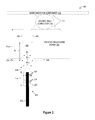
- FIG. 2 illustrates a partial cross-sectional view of a test probe device having a conductive elastomer test probe tip that is positioned for insertion into a back-drilled plated through hole via in accordance with selected embodiments of the present invention
- FIG. 3 illustrates a partial cross-sectional view of a test probe device having a conductive elastomer test probe tip that is fully inserted into a back-drilled plated through hole via formed in the board to make electrical contact with the plating layer(s) in accordance with selected embodiments of the present invention
- FIG. 4 illustrates a flow diagram fir a design and manufacturing sequence for fabricating and/or using a test probe device having a conductive elastomer test probe tip to test a printed circuit or wiring board assembly in accordance with selected embodiments of the present invention.
- a test probe having a conductive elastomer tip and associated methodology of fabrication and/or operation are described for testing printed circuit board assemblies having back-drilled plated through holes.
- a test probe includes a flexible or elastic tip structure having predetermined geometric shape dimensions and conductive properties that are suitable for insertion into a back-drilled plated through hole to make electrical contact with back-drilled plating layer(s) in the plated through hole.
- the elastic tip structure may be formed by spray coating or molding a conductive elastomer material, such as a metal impregnated polymer, on the tip or distal end region of a probe.
- the elastic tip structure may be formed with a chemically bonded conductive or non-conductive polymer matrix containing conductive particles which are positioned and dispersed throughout the polymer matrix to provide a conductive path from the remaining back-drilled plating layer(s) to the probe when inserted and compressed into contact with the back-drilled plating layer(s).
- the conductive particles are positioned and dispersed in the polymer matrix so that the conductive particles do not electrically contact one another when the elastic tip structure is not compressed and so that there is no conductive path through the uncompressed elastic tip structure.
- the width of the elastic tip structure is suitably dispose to fit within a specified through-hole width while making electrical or “wiping” contact with the remaining back-drilled plating layer(s) in the plated through hole(s).
- the elastic tip structure may be positioned to provide a contact wiping action during insertion into the plated through hole without damaging or scratching the remaining back-drilled plating layer(s) inside the plated through hole.
- FIG. 1 there is shown a partial cross-sectional view of an electronic package 10 in which a semiconductor chip 12 is mounted onto a circuitized substrate carrier 14 (e.g., a printed circuit board) which includes a multilayer interconnect structure 20 with plated through hole conductors 21 - 24 and contact pads 26 - 28 for electronically interconnecting the semiconductor chip 12 through the printed circuit board 14 to circuit elements and traces 25 in the PCB 14 and/or to external circuits, such as one or more test probe devices 16 , 18 .
- a circuitized substrate carrier 14 e.g., a printed circuit board
- external circuits such as one or more test probe devices 16 , 18 .
- the semiconductor chip 12 is attached for electrical communication to the circuitized substrate carrier with a plurality of microvias or contact members 30 (e.g., solder connections) and contact pads 32 which are in electrical contact with a plurality of electrically conductive connectors 28 formed on the circuitized substrate carrier 14 .
- a layer of electrically conductive material 34 e.g., copper, conductive paste or solder
- a pattern of solder connections 34 may be formed to match the pattern of microvia contact members 30 on semiconductor chip 12 .
- each patterned conductor of electrically conductive material 34 is formed to make electrical contact with a contact pad 28 corresponding to a plated through hole or through-via 1 , 2 formed in the circuitized substrate carrier 14 .
- the circuitized substrate carrier 14 may be formed as a multilayer interconnect structure 20 having alternating layers of dielectric and conductive materials to define the circuit elements and traces 25 .
- any desired circuitized substrate carrier 14 may be used, such as a conventional printed wiring board substrate having layers of glass reinforced epoxy laminate 29 a - d to encapsulate various layers of circuitry formed with circuit elements and traces 25 .
- the various layers of circuitry in the circuitized substrate carrier 14 are electrically interconnected to one another and to the semiconductor chip 12 by the plated through hole or through-via 1 , 2 which may be formed by drilling holes (e.g., with a laser drill) that intersect the circuit features that are to be connected and then plating the walls of the holes with conductive plating layers 21 - 24 to form electrical connections.
- the conductive plating layers 21 - 24 connect the various layers of circuitry in the circuitized substrate carrier 14 with the contact pads 26 - 28 formed on the front and back exterior surfaces of the circuitized substrate carrier 14 .
- the exterior surface metal used to form the contact pads 26 - 28 may be patterned to provide lands surrounding the plated through holes (e.g, 1 ) which are larger than the diameters of the holes.
- selected ones of the microvia contact members 30 may be provided with a direct electrical path through the circuitized substrate carrier 14 by using a plated through hole or through-via (e.g., PTH 1 ) to connect the semiconductor chip 12 across a respective microvia contact member 30 , solder connection 34 , contact pad 32 , contact pad 28 , PTH planting layers 21 - 22 , and landing contact pads 26 - 27 .
- test probe devices e.g., 16 , 18
- the landing contact pads 26 - 27 may be applied to the landing contact pads 26 - 27 to probe the semiconductor chip 12 and/or any of the various layers of circuitry in the circuitized substrate carrier 14 that are interconnected to the plated through hole or through-via 1 .
- FIG. 1 also shows that aback-drilled plated through hole/via 2 may be formed by removing unused portions of the plated through hole conductor layers 23 - 24 (indicated with dashed lines) which form stubs that can create potential signal integrity problems, signal delays, and other undesired electrical effects.
- aback-drilled plated through hole/via 2 may be formed by removing unused portions of the plated through hole conductor layers 23 - 24 (indicated with dashed lines) which form stubs that can create potential signal integrity problems, signal delays, and other undesired electrical effects.
- plated through hole or through-via structures in a multi-layered printed circuit board include unused lengths of the PTH via structure 2 in a signal path (indicated with dashed lines) which are not connected to any circuit elements and traces 25 in the PCB 14 , the unused portion of the PTH via structure 2 can behave as a transmission line open stub in parallel with the signal transmission path.
- back drilling may be employed to remove extraneous plating layers from the PTH via structures that are not connected to the internal wiring of the circuitized substrate carrier 14 .
- Back drilling can be implemented using any desired technique, such as by drilling openings in the bottom of the PCB 14 having a radius slightly larger than the via opening (e.g., 2 ) to drill out and remove the conductive plating layers 23 - 24 from the bottom portion of the PTH 2 , thereby reducing the length of the stab and the resonance effects on signals.
- the removal the stub also severs the electrical conductive path in the PTH via structure that is used for probe testing of the printed circuit board assembly. As shown in FIG.
- the undrilled PTH 1 still provides the direct electrical path that is needed for probe testing (e.g., with probe device 16 ), but because the back-drilled PTH 2 no longer provides an electrical path connection that can be used by the probe device (e.g., 18 ), the traditional method of probing the bottom surface of the circuitized substrate carrier 14 that is directly opposite the mounted semiconductor chip 12 is no longer possible.
- Existing solutions for probe testing back-drilled PTH via structures impose additional cost and complexity (e.g., by requiring boundary scan circuits in the PCB), limit the ability to detect interconnect defects (until after boundary scan testing is performed), and/or require specialized test probes having spring geometry contacts that can damage the back-drilled PTH.
- test probe devices 16 , 18 are not configured to penetrate into the back-drilled PTH and mike contact with the back-drilled plating layers 23 - 24 .
- the test probes 16 - 18 are suitable for making electrical contact with the landing contact pads 26 - 27 for the first PTH 1 , neither can be used with the second PTH 2 .
- the first test probe 16 is narrow enough for partial insertion into the PTH 2 , but is not long enough to make electrical contact with the back-drilled plating layers 23 - 24 .
- the second test probe 18 is too wide to be inserted into the PTH 2 and cannot make electrical contact with the back-drilled plating layers 23 - 24 .
- FIG. 2 illustrates a partial cross-sectional view 100 of a test probe device 201 having a conductive elastomer test probe tip 203 that is positioned for insertion into a back-drilled plated through hole via 106 formed in a printed circuit or wire board 101 .
- a semiconductor component 112 may be mounted onto the printed circuit/wire board 101 using any desired conductor and attachment mechanism, such as solder ball conductors or other connectors 110 which are electronically attached and connected with one or more layers of electrically conductive material 111 (e.g., copper, conductive paste or solder) to plated through hole conductors and/or contact pads 103 formed on the printed circuit or wire board 101 .
- electrically conductive material 111 e.g., copper, conductive paste or solder
- the printed circuit/wire board 101 is formed with one or more layers of dielectric and conductive materials to form a substrate carrier. Though not shown, it will be appreciated that the printed circuit/wire board 101 may be a multilayer circuitized substrate in which various layers of circuitry are formed with circuit elements and other conductive traces.
- one or more plated through holes or through-vias 106 are formed, such as by laser drilling holes or via openings and then plating the walls of the openings with conductive plating layers 102 - 105 to form electrical connections on the top and bottom surfaces of the printed circuit/wire board 101 and on the interior walls of the openings. Subsequently, back-drilling is applied to form the back-drilled plated through hole via 106 .
- the resulting back-drilled plated through hole via 106 is defined by a plurality of geometric dimensional measures, including a recess depth dimension (D PL ) which is a predetermined percentage of the total depth (D PCB ) of the printed circuit/wire board 101 .
- D PL recess depth dimension
- D PCB total depth dimension
- the specified depth dimensions D PL , D PCB may be measured from the bottom of the contact pads 104 - 105 as shown, from the bottom of the printed circuit/wire board 101 (not shown), or in any desired manner.
- the geometric dimensional measures of the back-drilled plated through hole via 106 may also include a first width dimension (W PL ) of the total width between the remaining PTH plating layers 102 , 103 , and a second width dimension (W VIA ) of the total width of the back-drilled via opening formed in the printed circuit/wire board 101 .
- W PL first width dimension
- W VIA second width dimension
- the second width dimension (W VIA ) is larger than the first width dimension (W PL ) by a difference that is equal to or greater than the combined thickness of the PTH plating layers 102 , 103 .
- the plurality of geometric dimensional measures defining the back-drilled plated through hole via 106 may be maintained within specified tolerance measures for the various width and depth measures, thereby providing consistent and repeatable feature dimensions for the back-drilled plated through hole via 106 .
- the electrical test probe device 201 is provided with a conductive elastomer test probe tip 203 having predetermined geometric dimensions to fit within the width (W VIA ) of the plated through hole via 106 while making electrical or “wiping” contact with the remaining plating layer(s) 102 - 103 .
- the conductive elastomer test probe tip 203 is secured at one end of the probe body 202 using any desired attachment mechanism.
- the conductive elastomer test probe tip 203 may be formed by spray coating or molding a conductive elastomer material, such as a metal impregnated polymer, on the tip or distal end region of the probe body 202 .
- the surface of the tip or distal end region of the probe body 202 may be abraded or slotted to promote engagement with the conductive elastomer material 203 .
- the conductive elastomer test probe tip 203 may be formed with a chemically bonded conductive or non-conductive polymer matrix containing conductive particles 204 , 205 which are positioned and dispersed throughout the polymer matrix 203 to provide a conductive path when compressed into contact with one another, but to otherwise not provide a conductive path when uncompressed (as shown in FIG. 2 ).
- the conductive elastomer test probe tip 203 may be formed with conductive particles 204 - 205 (e.g., silver or other metal) that are grafted to or dispersed within a conductive or non-conductive polymer substrate material 203 , such as by spraying a slurry or elastomer spray solution consisting of a mixture of melted rubber or other elastomer material (to provide elasticity or resilience, metal particles (to provide electrical conductive paths), and volatile solvent (to reduce viscosity during spraying) to a (predetermined thickness around the probe body 202 .
- a slurry or elastomer spray solution consisting of a mixture of melted rubber or other elastomer material (to provide elasticity or resilience, metal particles (to provide electrical conductive paths), and volatile solvent (to reduce viscosity during spraying) to a (predetermined thickness around the probe body 202 .
- a slurry containing conductive particles can be molded, screen printed, or rotationally sprayed around the tip or distal end region of the probe body 202 to form the conductive elastomer test probe tip 203 .
- the conductive elastomer test probe tip 203 may be formed by molding or extruding a conductive etastomer material, such as a metal impregnated polymer, to cover the tip or distal end region of the probe body 202 .
- the conductive elastomer test probe tip 203 is shown as having a limited number of conductive particles 204 , 205 formed in the polymer matrix 203 , it will be appreciated that any desired quantity of conductive particles may positioned or dispersed in the polymer matrix 203 with sufficiently proximity to each other to provide a desired level of conductivity or non-conductivity, as the case may be.
- the geometric dimensions of the conductive elastomer test probe tip 203 may be controlled to provide a minimum coverage length for the probe tip/distal end region (L TIP ) which may also include a specified end length (L END ) for an extension of the conductive elastomer test probe tip 203 past the end of the end of the probe body 202 .
- the minimum coverage length for the probe tip/distal end region (L TIP ) should be larger than the recess depth dimension (D PL ) of the back-drilled plated through hole via 106 .
- the geometric dimensions of the conductive elastomer test probe tip 203 are controlled to provide a specified thickness measure so that the total width (W TIP ) or diameter measure of the conductive elastomer test probe tip 203 is smaller than the through via diameter or width dimension (W VIA ), but larger than the plated through via diameter or width dimension (W PL ).
- W TIP total width
- W VIA through via diameter or width dimension
- W PL plated through via diameter or width dimension
- W PL ⁇ W TIP ⁇ W VIA .
- W PL ⁇ W TIP ⁇ W VIA .
- the conductive elastomer test probe tip 203 will fit within the through-hole width (W VIA ) while making electrical or “wiping” contact with the remaining plating layer(s) 102 - 103 which are separated by the plating layer separation width (W PL ) to provide a 360 degree contact surface with the PTH via structure 106 .
- the geometric dimensional measures defining the conductive elastomer test probe tip 203 may be maintained within specified tolerance measures for the various width and length measures, thereby providing consistent and repeatable feature dimensions for the elastomer test probe tip 203 .
- FIG. 3 shows illustrates a partial cross-sectional view 200 of the test probe device 201 with the conductive elastomer test probe tip 203 that is partially or fully inserted into the back-drilled plated through hole via 106 formed in the printed circuit/wire board 101 .
- the conductive particles 205 A in the compressed portion of the conductive elastomer test probe tip 203 are pressed together with the compressed polymer matrix 203 to provide a conductive path from the back-drilled plating layers (e.g., 103 ) to the probe body 202 .
- the conductive particles 205 A in the metal impregnated elastomer 203 touch or contact one another in the compressed area.
- the conductive particles 204 in the metal impregnated elastomer 203 do not touch or contact one another, so there is no electrical path formed.
- FIG. 4 there is shown a flow diagram for a design and manufacturing sequence 300 for fabricating and/or using a test probe device having a conductive elastomer test probe tip for testing a printed circuit or wiring board assembly in accordance with selected embodiments of the present invention.
- the sequence may begin at step 301 during an initial design and/or fabrication of a printed circuit board assembly.
- plated through hole connections are formed in the printed circuit board, alone or in combination with one or more mounted integrated circuits.
- the plated through holes may be formed by drilling holes (e.g., with a laser drill) in the printed circuit board, and then plating the walls of the holes with conductive plating layers to form plated through hole connections.
- the plated through hole connections are back drilled to remove any unused portions of the plated through hole connections (or stubs) and to leave remnant plating layers in the plated through holes.
- back drilling may be performed by drilling the bottoms of the plated through hole connections with back-drilled openings having a radius that is slightly larger than the radius of the originally drilled holes to drill out and remove the plating layers from the bottom portion of the printed circuit board, thereby reducing the length of the stub and thus reduce the resonance effects on signals.
- the back-drilled PTH connections are defined by one or more recess depth dimensions (D PL ), the back-drilled PTH connections no longer provide a path of electrical continuity through the entire width of the printed circuit board that can be used with conventional test probe devices.
- the test probe may include a conductive probe body having a tip or distal end region with a minimum specified length that is disposed to promote electrical contact with the back-drilled plating layers.
- the minimum specified length of the tip or distal end region (L TIP ) should be larger than the recess depth dimension (D PL ) of the back-drilled PTH connection.
- the tip or distal end region of the test probe may be disposed to promote adhesion with a subsequently formed conductive elastomer coating, such as by including an abraded or roughened or slotted surface to promote engagement with the conductive elastomer material.
- a conductive elastomer coating or structure is formed on the tip or distal end of the test probe.
- the tip of the test probe may be coated with a resilient electrical conductive elastomer that will make contact with the remaining plating layers in the back-drilled PTH connection.
- An example of an electrical conductive polymer film is a carbon or silver impregnated silicone compound.
- the test probe tip may be uniformly coated with a controlled thickness of conductive elastomer coating so that the total width (W TIP ) of the conductive elastomer test probe tip is larger than the plating layer separation width (W PL ).
- the elastomer-coated test probe is positioned in the back-drilled PTH connection to establish electrical contact between the test probe and the remaining plating layers in the back-drilled PTH connection.
- the compressive properties of the conductive elastomer coating provides a normal or compressive force when inserted into contact with the back-drilled plating layers inside the PTH connection that is necessary to make adequate electrical contact.
- W TIP the width of the conductive elastomer coating/structure on the test probe tip
- W PL plating layer separation width
- the elastomer-coated test probe provides a contact wiping action when the test probe is inserted into the back-drilled PTH connection where it will make contact with the remaining plating layers. The wiping action of the probe insertion will remove copper oxidation from the back-drilled plating layers to create a clean contact area.
- one or more probe tests are performed with the elastomer-coated test probe positioned and inserted for electrical contact with the back-drilled PTH connection.
- the probe can enter into the back drilled PTH connection to make electrical contact with the back-drilled plated layers.
- the resilient tip of the elastomer-coated test probe will provide a contact wiping action during insertion into the back-drilled PTH without damaging or scratching the plating layers inside the back-drilled PTH connection.
- the cylindrical shape of the rotationally sprayed test probe tip will provide a 360 degree surface of contact inside the back-drilled PTH connection.
- the test probe is removed and may be relocated to test another back-drilled PTH connection. In this way, a single test probe configuration may be used in manual testing of the back-drilled PTH connection. Alternatively, the test probe configuration described herein may be arranged into multiple probe array pattern for use in performing in-circuit testing (ICT) of the PCB.
- ICT in-circuit testing
Landscapes
- Physics & Mathematics (AREA)
- General Physics & Mathematics (AREA)
- Geometry (AREA)
- Measuring Leads Or Probes (AREA)
- Engineering & Computer Science (AREA)
- Computer Hardware Design (AREA)
- Microelectronics & Electronic Packaging (AREA)
- General Engineering & Computer Science (AREA)
Abstract
Description
Claims (7)
Priority Applications (1)
| Application Number | Priority Date | Filing Date | Title |
|---|---|---|---|
| US13/938,688 US9459285B2 (en) | 2013-07-10 | 2013-07-10 | Test probe coated with conductive elastomer for testing of backdrilled plated through holes in printed circuit board assembly |
Applications Claiming Priority (1)
| Application Number | Priority Date | Filing Date | Title |
|---|---|---|---|
| US13/938,688 US9459285B2 (en) | 2013-07-10 | 2013-07-10 | Test probe coated with conductive elastomer for testing of backdrilled plated through holes in printed circuit board assembly |
Publications (2)
| Publication Number | Publication Date |
|---|---|
| US20150015288A1 US20150015288A1 (en) | 2015-01-15 |
| US9459285B2 true US9459285B2 (en) | 2016-10-04 |
Family
ID=52276618
Family Applications (1)
| Application Number | Title | Priority Date | Filing Date |
|---|---|---|---|
| US13/938,688 Active 2034-05-03 US9459285B2 (en) | 2013-07-10 | 2013-07-10 | Test probe coated with conductive elastomer for testing of backdrilled plated through holes in printed circuit board assembly |
Country Status (1)
| Country | Link |
|---|---|
| US (1) | US9459285B2 (en) |
Cited By (4)
| Publication number | Priority date | Publication date | Assignee | Title |
|---|---|---|---|---|
| DE102018101031A1 (en) | 2018-01-18 | 2019-07-18 | Xcerra Corp. | Test needle, test probe and finger tester for testing printed circuit boards |
| WO2019141777A1 (en) | 2018-01-18 | 2019-07-25 | Xcerra Corp. | Capacitive test needle for measuring electrically conductive layers in printed circuit board holes |
| US11362697B2 (en) * | 2016-12-16 | 2022-06-14 | Samsung Electronics Co., Ltd. | Multilayer printed circuit board and electronic device including the same |
| US20240008186A1 (en) * | 2022-06-30 | 2024-01-04 | International Business Machines Corporation | Real-time control of via stub drilling depth asymmetry |
Families Citing this family (36)
| Publication number | Priority date | Publication date | Assignee | Title |
|---|---|---|---|---|
| US9521754B1 (en) | 2013-08-19 | 2016-12-13 | Multek Technologies Limited | Embedded components in a substrate |
| US9554465B1 (en) | 2013-08-27 | 2017-01-24 | Flextronics Ap, Llc | Stretchable conductor design and methods of making |
| US10231333B1 (en) * | 2013-08-27 | 2019-03-12 | Flextronics Ap, Llc. | Copper interconnect for PTH components assembly |
| US9521748B1 (en) | 2013-12-09 | 2016-12-13 | Multek Technologies, Ltd. | Mechanical measures to limit stress and strain in deformable electronics |
| US9338915B1 (en) | 2013-12-09 | 2016-05-10 | Flextronics Ap, Llc | Method of attaching electronic module on fabrics by stitching plated through holes |
| US9807869B2 (en) | 2014-11-21 | 2017-10-31 | Amphenol Corporation | Mating backplane for high speed, high density electrical connector |
| KR20170096258A (en) * | 2016-02-15 | 2017-08-24 | 삼성전자주식회사 | Testing apparatus |
| CN109076700B (en) | 2016-03-08 | 2021-07-30 | 安费诺公司 | Backplane footprint for high-speed, high-density electrical connectors |
| US10201074B2 (en) | 2016-03-08 | 2019-02-05 | Amphenol Corporation | Backplane footprint for high speed, high density electrical connectors |
| US9935024B2 (en) * | 2016-04-28 | 2018-04-03 | Taiwan Semiconductor Manufacturing Co., Ltd. | Method for forming semiconductor structure |
| JP6737002B2 (en) * | 2016-06-17 | 2020-08-05 | オムロン株式会社 | Probe pin |
| US11257724B2 (en) * | 2016-08-08 | 2022-02-22 | Semiconductor Components Industries, Llc | Semiconductor wafer and method of probe testing |
| US11075129B2 (en) | 2016-08-08 | 2021-07-27 | Semiconductor Components Industries, Llc | Substrate processing carrier |
| US10461000B2 (en) * | 2016-08-08 | 2019-10-29 | Semiconductor Components Industries, Llc | Semiconductor wafer and method of probe testing |
| US9793186B1 (en) * | 2016-08-08 | 2017-10-17 | Semiconductor Components Industries, Llc | Semiconductor wafer and method of backside probe testing through opening in film frame |
| US10859598B1 (en) * | 2018-02-27 | 2020-12-08 | Tektronix, Inc. | Back-drilled via attachment technique using a UV-cure conductive adhesive |
| US10917976B1 (en) * | 2017-07-12 | 2021-02-09 | Juniper Networks, Inc. | Designing a printed circuit board (PCB) to detect slivers of conductive material included within vias of the PCB |
| US10345136B2 (en) * | 2017-07-14 | 2019-07-09 | International Business Machines Corporation | Adjustable load transmitter |
| US10527649B2 (en) | 2017-07-14 | 2020-01-07 | International Business Machines Corporation | Probe card alignment |
| IT201700100522A1 (en) * | 2017-09-07 | 2019-03-07 | Technoprobe Spa | Interface element for an electronic device test device and its manufacturing method |
| WO2019241107A1 (en) * | 2018-06-11 | 2019-12-19 | Amphenol Corporation | Backplane footprint for high speed, high density electrical connectors |
| US11355403B2 (en) * | 2018-06-28 | 2022-06-07 | Western Digital Technologies, Inc. | Semiconductor device including through-package debug features |
| TWI855075B (en) | 2019-05-20 | 2024-09-11 | 美商安芬諾股份有限公司 | Connector module, connector, electronic assembly, electrical connector and wafer of connector module |
| TWI822833B (en) * | 2019-08-15 | 2023-11-21 | 優顯科技股份有限公司 | Electronic detection interface, electronic detection module using the same, and electronic detection method applicable of the same |
| US11637389B2 (en) | 2020-01-27 | 2023-04-25 | Amphenol Corporation | Electrical connector with high speed mounting interface |
| CN120566112A (en) | 2020-01-27 | 2025-08-29 | 安费诺有限公司 | Electrical connector with high-speed mounting interface |
| KR102132860B1 (en) * | 2020-03-17 | 2020-07-10 | 주식회사 나노시스 | Printed circuit board test system |
| TWM601814U (en) * | 2020-05-13 | 2020-09-21 | 金像電子股份有限公司 | Measurement system |
| US11885830B2 (en) * | 2021-01-15 | 2024-01-30 | Lumentum Operations Llc | Probe tip assembly for testing optical components |
| US12560422B2 (en) | 2021-03-24 | 2026-02-24 | Nanjing Taliang Technology Co., Ltd. | Optical system for measuring the depth of an inner layer of a printed circuit board |
| CN114092560B (en) * | 2021-12-01 | 2025-03-11 | 深圳市鹰眼在线电子科技有限公司 | Back-drilled hole 2D/3D feature measurement system, method and device |
| USD1067191S1 (en) | 2021-12-14 | 2025-03-18 | Amphenol Corporation | Electrical connector |
| USD1068685S1 (en) | 2021-12-14 | 2025-04-01 | Amphenol Corporation | Electrical connector |
| JP7836705B2 (en) * | 2022-04-27 | 2026-03-27 | メクテック株式会社 | Flexible printed circuit boards and electrical wiring |
| CN117148227A (en) * | 2022-05-23 | 2023-12-01 | 中兴智能科技南京有限公司 | Measuring connector structural parts and PCB |
| US20250389764A1 (en) * | 2024-06-19 | 2025-12-25 | International Business Machines Corporation | Evaluating copper plating in a pth |
Citations (25)
| Publication number | Priority date | Publication date | Assignee | Title |
|---|---|---|---|---|
| US3992073A (en) | 1975-11-24 | 1976-11-16 | Technical Wire Products, Inc. | Multi-conductor probe |
| US5166602A (en) | 1991-11-07 | 1992-11-24 | Compaq Computer Corporation | Elastomeric probe apparatus and associated methods |
| JPH0846311A (en) | 1994-07-26 | 1996-02-16 | Advantest Corp | Electrode pad for connecting electric signal |
| US5527591A (en) * | 1994-12-02 | 1996-06-18 | Augat Inc. | Electrical contact having a particulate surface |
| US5600099A (en) * | 1994-12-02 | 1997-02-04 | Augat Inc. | Chemically grafted electrical devices |
| US5855063A (en) | 1996-05-28 | 1999-01-05 | Packard Hughes Interconnect Company | Method of making contact pad having metallically anchored elastomeric electrical contacts |
| US5879172A (en) | 1997-04-03 | 1999-03-09 | Emulation Technology, Inc. | Surface mounted adapter using elastomeric conductors |
| US5949029A (en) * | 1994-08-23 | 1999-09-07 | Thomas & Betts International, Inc. | Conductive elastomers and methods for fabricating the same |
| US6051982A (en) | 1996-08-02 | 2000-04-18 | International Business Machines Corporation | Electronic component test apparatus with rotational probe and conductive spaced apart means |
| US6264476B1 (en) * | 1999-12-09 | 2001-07-24 | High Connection Density, Inc. | Wire segment based interposer for high frequency electrical connection |
| US6297660B2 (en) * | 1999-01-13 | 2001-10-02 | Micron Technology, Inc. | Test carrier with variable force applying mechanism for testing semiconductor components |
| US6400167B1 (en) | 2000-08-21 | 2002-06-04 | Tektronix, Inc. | Probe tip adapter for a measurement probe |
| US6423905B1 (en) | 2000-05-01 | 2002-07-23 | International Business Machines Corporation | Printed wiring board with improved plated through hole fatigue life |
| US6538213B1 (en) | 2000-02-18 | 2003-03-25 | International Business Machines Corporation | High density design for organic chip carriers |
| US6702587B2 (en) | 2001-08-08 | 2004-03-09 | Paricon Technologies Corporation | Separable electrical connector using anisotropic conductive elastomer interconnect medium |
| US20040051541A1 (en) | 2002-09-04 | 2004-03-18 | Yu Zhou | Contact structure with flexible cable and probe contact assembly using same |
| US20050134298A1 (en) | 2003-12-18 | 2005-06-23 | Lecroy Corporation | Resistive probe tips |
| US7337537B1 (en) * | 2003-09-22 | 2008-03-04 | Alcatel Lucent | Method for forming a back-drilled plated through hole in a printed circuit board and the resulting printed circuit board |
| US20080217052A1 (en) * | 2007-03-07 | 2008-09-11 | Fujitsu Limited | Wiring board and method of manufacturing wiring board |
| US20090049414A1 (en) | 2007-08-16 | 2009-02-19 | International Business Machines Corporation | Method and system for reducing via stub resonance |
| US20090111299A1 (en) | 2007-10-31 | 2009-04-30 | International Business Machines Corporation | Surface Mount Array Connector Leads Planarization Using Solder Reflow Method |
| US7538565B1 (en) | 1992-10-19 | 2009-05-26 | International Business Machines Corporation | High density integrated circuit apparatus, test probe and methods of use thereof |
| US7669321B1 (en) * | 2005-07-13 | 2010-03-02 | Cisco Technology, Inc. | Methods for verifying correct counter-bore depth and precision on printed circuit boards |
| US20100052715A1 (en) | 1992-10-19 | 2010-03-04 | International Business Machines Corporation | High density integrated circuit apparatus, test probe and methods of use thereof |
| US20120298406A1 (en) | 2011-05-23 | 2012-11-29 | International Business Machines Corporation | Reduced stress gull wing solder joints for printed wiring board connections |
-
2013
- 2013-07-10 US US13/938,688 patent/US9459285B2/en active Active
Patent Citations (25)
| Publication number | Priority date | Publication date | Assignee | Title |
|---|---|---|---|---|
| US3992073A (en) | 1975-11-24 | 1976-11-16 | Technical Wire Products, Inc. | Multi-conductor probe |
| US5166602A (en) | 1991-11-07 | 1992-11-24 | Compaq Computer Corporation | Elastomeric probe apparatus and associated methods |
| US20100052715A1 (en) | 1992-10-19 | 2010-03-04 | International Business Machines Corporation | High density integrated circuit apparatus, test probe and methods of use thereof |
| US7538565B1 (en) | 1992-10-19 | 2009-05-26 | International Business Machines Corporation | High density integrated circuit apparatus, test probe and methods of use thereof |
| JPH0846311A (en) | 1994-07-26 | 1996-02-16 | Advantest Corp | Electrode pad for connecting electric signal |
| US5949029A (en) * | 1994-08-23 | 1999-09-07 | Thomas & Betts International, Inc. | Conductive elastomers and methods for fabricating the same |
| US5527591A (en) * | 1994-12-02 | 1996-06-18 | Augat Inc. | Electrical contact having a particulate surface |
| US5600099A (en) * | 1994-12-02 | 1997-02-04 | Augat Inc. | Chemically grafted electrical devices |
| US5855063A (en) | 1996-05-28 | 1999-01-05 | Packard Hughes Interconnect Company | Method of making contact pad having metallically anchored elastomeric electrical contacts |
| US6051982A (en) | 1996-08-02 | 2000-04-18 | International Business Machines Corporation | Electronic component test apparatus with rotational probe and conductive spaced apart means |
| US5879172A (en) | 1997-04-03 | 1999-03-09 | Emulation Technology, Inc. | Surface mounted adapter using elastomeric conductors |
| US6297660B2 (en) * | 1999-01-13 | 2001-10-02 | Micron Technology, Inc. | Test carrier with variable force applying mechanism for testing semiconductor components |
| US6264476B1 (en) * | 1999-12-09 | 2001-07-24 | High Connection Density, Inc. | Wire segment based interposer for high frequency electrical connection |
| US6538213B1 (en) | 2000-02-18 | 2003-03-25 | International Business Machines Corporation | High density design for organic chip carriers |
| US6423905B1 (en) | 2000-05-01 | 2002-07-23 | International Business Machines Corporation | Printed wiring board with improved plated through hole fatigue life |
| US6400167B1 (en) | 2000-08-21 | 2002-06-04 | Tektronix, Inc. | Probe tip adapter for a measurement probe |
| US6702587B2 (en) | 2001-08-08 | 2004-03-09 | Paricon Technologies Corporation | Separable electrical connector using anisotropic conductive elastomer interconnect medium |
| US20040051541A1 (en) | 2002-09-04 | 2004-03-18 | Yu Zhou | Contact structure with flexible cable and probe contact assembly using same |
| US7337537B1 (en) * | 2003-09-22 | 2008-03-04 | Alcatel Lucent | Method for forming a back-drilled plated through hole in a printed circuit board and the resulting printed circuit board |
| US20050134298A1 (en) | 2003-12-18 | 2005-06-23 | Lecroy Corporation | Resistive probe tips |
| US7669321B1 (en) * | 2005-07-13 | 2010-03-02 | Cisco Technology, Inc. | Methods for verifying correct counter-bore depth and precision on printed circuit boards |
| US20080217052A1 (en) * | 2007-03-07 | 2008-09-11 | Fujitsu Limited | Wiring board and method of manufacturing wiring board |
| US20090049414A1 (en) | 2007-08-16 | 2009-02-19 | International Business Machines Corporation | Method and system for reducing via stub resonance |
| US20090111299A1 (en) | 2007-10-31 | 2009-04-30 | International Business Machines Corporation | Surface Mount Array Connector Leads Planarization Using Solder Reflow Method |
| US20120298406A1 (en) | 2011-05-23 | 2012-11-29 | International Business Machines Corporation | Reduced stress gull wing solder joints for printed wiring board connections |
Non-Patent Citations (2)
| Title |
|---|
| IPCOM000135653D: "Conductive Elastomeric Tipped Probe for Testing Fine Pitched Conductors" Disclosed Anonymously, Apr. 20, 2006, (four pages). |
| Shaowei Deng et al., Effects of Open Stubs Associated with Plated Through-Hole Vias in Backpanel Designs, 2004 International Symposium on Electromagnetic Compatibility, vol. 3, Aug. 9-13, 2004, (six pages). |
Cited By (6)
| Publication number | Priority date | Publication date | Assignee | Title |
|---|---|---|---|---|
| US11362697B2 (en) * | 2016-12-16 | 2022-06-14 | Samsung Electronics Co., Ltd. | Multilayer printed circuit board and electronic device including the same |
| DE102018101031A1 (en) | 2018-01-18 | 2019-07-18 | Xcerra Corp. | Test needle, test probe and finger tester for testing printed circuit boards |
| WO2019141777A1 (en) | 2018-01-18 | 2019-07-25 | Xcerra Corp. | Capacitive test needle for measuring electrically conductive layers in printed circuit board holes |
| US11774495B2 (en) | 2018-01-18 | 2023-10-03 | Atg Luther & Maelzer Gmbh | Capacitive test needle for measuring electrically conductive layers in printed circuit board holes |
| EP4471435A2 (en) | 2018-01-18 | 2024-12-04 | atg Luther & Maelzer GmbH | Test needle, test probe and finger tester for testing printed circuit boards |
| US20240008186A1 (en) * | 2022-06-30 | 2024-01-04 | International Business Machines Corporation | Real-time control of via stub drilling depth asymmetry |
Also Published As
| Publication number | Publication date |
|---|---|
| US20150015288A1 (en) | 2015-01-15 |
Similar Documents
| Publication | Publication Date | Title |
|---|---|---|
| US9459285B2 (en) | Test probe coated with conductive elastomer for testing of backdrilled plated through holes in printed circuit board assembly | |
| US8115110B2 (en) | Printed circuit board minimizing undesirable signal reflections in a via and methods therefor | |
| CN111937254B (en) | Controlled Impedance Metallized Plastic Receptacle | |
| TW201723488A (en) | Coaxial integrated circuit test socket | |
| US9806474B2 (en) | Printed circuit board having high-speed or high-frequency signal connector | |
| US20040140821A1 (en) | Test PCB and contactor for testing of electronic device | |
| US8508248B1 (en) | Testing vias formed in printed circuit boards | |
| JP2018538693A (en) | Circuit board with pocket | |
| TWI448707B (en) | Semiconductor test device | |
| US20090058425A1 (en) | Method and apparatus to test electrical continuity and reduce loading parasitics on high-speed signals | |
| KR101254180B1 (en) | Test socket for testing semiconductor | |
| US7518384B2 (en) | Method and apparatus for manufacturing and probing test probe access structures on vias | |
| EP3340747A1 (en) | Multi-layer ic socket with an integrated impedance matching network | |
| US20150351229A1 (en) | Printed circuit board comprising co-planar surface pads and insulating dielectric | |
| US20020166696A1 (en) | Land grid array (LGA) pad repair structure and method | |
| KR20090070017A (en) | Interposer of Probe Card and Manufacturing Method Thereof | |
| US20060103397A1 (en) | Method and apparatus for a twisting fixture probe for probing test access point structures | |
| US20060022692A1 (en) | Backside attach probe, components thereof, and methods for making and using same | |
| US8598466B2 (en) | Controlled-impedance electronic board vias, method of forming the same, and unitized PCB incorporating the same | |
| US20250227837A1 (en) | Selective removal of adhesive from coverlay for printed circuit board insulation | |
| US8390308B2 (en) | Testbed for testing electronic circuits and components | |
| US20250227854A1 (en) | Coverlay as printed circuit board (pcb) voltage insulator under connectors | |
| EP2096449B1 (en) | Testbed for testing electronic circuits and components | |
| KR20040067768A (en) | Contact Apparatus and Printed Circuit Board including the Contact Apparatus used for testing Microwave Device, and Manufacturing Method of the Printed Circuit Board | |
| US20230180397A1 (en) | Method and process for creating high-performance coax sockets |
Legal Events
| Date | Code | Title | Description |
|---|---|---|---|
| AS | Assignment |
Owner name: INTERNATIONAL BUSINESS MACHINES CORPORATION, NEW Y Free format text: ASSIGNMENT OF ASSIGNORS INTEREST;ASSIGNOR:MA, WAI MON;REEL/FRAME:030768/0965 Effective date: 20130709 |
|
| AS | Assignment |
Owner name: GLOBALFOUNDRIES U.S. 2 LLC, NEW YORK Free format text: ASSIGNMENT OF ASSIGNORS INTEREST;ASSIGNOR:INTERNATIONAL BUSINESS MACHINES CORPORATION;REEL/FRAME:036550/0001 Effective date: 20150629 |
|
| AS | Assignment |
Owner name: GLOBALFOUNDRIES INC., CAYMAN ISLANDS Free format text: ASSIGNMENT OF ASSIGNORS INTEREST;ASSIGNORS:GLOBALFOUNDRIES U.S. 2 LLC;GLOBALFOUNDRIES U.S. INC.;REEL/FRAME:036779/0001 Effective date: 20150910 |
|
| STCF | Information on status: patent grant |
Free format text: PATENTED CASE |
|
| AS | Assignment |
Owner name: WILMINGTON TRUST, NATIONAL ASSOCIATION, DELAWARE Free format text: SECURITY AGREEMENT;ASSIGNOR:GLOBALFOUNDRIES INC.;REEL/FRAME:049490/0001 Effective date: 20181127 |
|
| MAFP | Maintenance fee payment |
Free format text: PAYMENT OF MAINTENANCE FEE, 4TH YEAR, LARGE ENTITY (ORIGINAL EVENT CODE: M1551); ENTITY STATUS OF PATENT OWNER: LARGE ENTITY Year of fee payment: 4 |
|
| AS | Assignment |
Owner name: GLOBALFOUNDRIES U.S. INC., CALIFORNIA Free format text: ASSIGNMENT OF ASSIGNORS INTEREST;ASSIGNOR:GLOBALFOUNDRIES INC.;REEL/FRAME:054633/0001 Effective date: 20201022 |
|
| AS | Assignment |
Owner name: GLOBALFOUNDRIES INC., CAYMAN ISLANDS Free format text: RELEASE BY SECURED PARTY;ASSIGNOR:WILMINGTON TRUST, NATIONAL ASSOCIATION;REEL/FRAME:054636/0001 Effective date: 20201117 |
|
| AS | Assignment |
Owner name: GLOBALFOUNDRIES U.S. INC., NEW YORK Free format text: RELEASE BY SECURED PARTY;ASSIGNOR:WILMINGTON TRUST, NATIONAL ASSOCIATION;REEL/FRAME:056987/0001 Effective date: 20201117 Owner name: GLOBALFOUNDRIES U.S. INC., NEW YORK Free format text: RELEASE OF SECURITY INTEREST;ASSIGNOR:WILMINGTON TRUST, NATIONAL ASSOCIATION;REEL/FRAME:056987/0001 Effective date: 20201117 |
|
| MAFP | Maintenance fee payment |
Free format text: PAYMENT OF MAINTENANCE FEE, 8TH YEAR, LARGE ENTITY (ORIGINAL EVENT CODE: M1552); ENTITY STATUS OF PATENT OWNER: LARGE ENTITY Year of fee payment: 8 |