US9443796B2 - Air trench in packages incorporating hybrid bonding - Google Patents
Air trench in packages incorporating hybrid bonding Download PDFInfo
- Publication number
- US9443796B2 US9443796B2 US13/895,122 US201313895122A US9443796B2 US 9443796 B2 US9443796 B2 US 9443796B2 US 201313895122 A US201313895122 A US 201313895122A US 9443796 B2 US9443796 B2 US 9443796B2
- Authority
- US
- United States
- Prior art keywords
- dielectric layer
- package
- surface dielectric
- metal pad
- air
- Prior art date
- Legal status (The legal status is an assumption and is not a legal conclusion. Google has not performed a legal analysis and makes no representation as to the accuracy of the status listed.)
- Expired - Fee Related, expires
Links
Images


Classifications
-
- H—ELECTRICITY
- H10—SEMICONDUCTOR DEVICES; ELECTRIC SOLID-STATE DEVICES NOT OTHERWISE PROVIDED FOR
- H10P—GENERIC PROCESSES OR APPARATUS FOR THE MANUFACTURE OR TREATMENT OF DEVICES COVERED BY CLASS H10
- H10P50/00—Etching of wafers, substrates or parts of devices
- H10P50/69—Etching of wafers, substrates or parts of devices using masks for semiconductor materials
- H10P50/691—Etching of wafers, substrates or parts of devices using masks for semiconductor materials for Group V materials or Group III-V materials
- H10P50/692—Etching of wafers, substrates or parts of devices using masks for semiconductor materials for Group V materials or Group III-V materials characterised by their composition, e.g. multilayer masks or materials
-
- H01L23/498—
-
- H01L24/93—
-
- H—ELECTRICITY
- H10—SEMICONDUCTOR DEVICES; ELECTRIC SOLID-STATE DEVICES NOT OTHERWISE PROVIDED FOR
- H10W—GENERIC PACKAGES, INTERCONNECTIONS, CONNECTORS OR OTHER CONSTRUCTIONAL DETAILS OF DEVICES COVERED BY CLASS H10
- H10W10/00—Isolation regions in semiconductor bodies between components of integrated devices
- H10W10/01—Manufacture or treatment
- H10W10/021—Manufacture or treatment of air gaps
-
- H—ELECTRICITY
- H10—SEMICONDUCTOR DEVICES; ELECTRIC SOLID-STATE DEVICES NOT OTHERWISE PROVIDED FOR
- H10W—GENERIC PACKAGES, INTERCONNECTIONS, CONNECTORS OR OTHER CONSTRUCTIONAL DETAILS OF DEVICES COVERED BY CLASS H10
- H10W10/00—Isolation regions in semiconductor bodies between components of integrated devices
- H10W10/20—Air gaps
-
- H—ELECTRICITY
- H10—SEMICONDUCTOR DEVICES; ELECTRIC SOLID-STATE DEVICES NOT OTHERWISE PROVIDED FOR
- H10W—GENERIC PACKAGES, INTERCONNECTIONS, CONNECTORS OR OTHER CONSTRUCTIONAL DETAILS OF DEVICES COVERED BY CLASS H10
- H10W20/00—Interconnections in chips, wafers or substrates
- H10W20/40—Interconnections external to wafers or substrates, e.g. back-end-of-line [BEOL] metallisations or vias connecting to gate electrodes
- H10W20/41—Interconnections external to wafers or substrates, e.g. back-end-of-line [BEOL] metallisations or vias connecting to gate electrodes characterised by their conductive parts
- H10W20/42—Vias, e.g. via plugs
-
- H—ELECTRICITY
- H10—SEMICONDUCTOR DEVICES; ELECTRIC SOLID-STATE DEVICES NOT OTHERWISE PROVIDED FOR
- H10W—GENERIC PACKAGES, INTERCONNECTIONS, CONNECTORS OR OTHER CONSTRUCTIONAL DETAILS OF DEVICES COVERED BY CLASS H10
- H10W20/00—Interconnections in chips, wafers or substrates
- H10W20/40—Interconnections external to wafers or substrates, e.g. back-end-of-line [BEOL] metallisations or vias connecting to gate electrodes
- H10W20/41—Interconnections external to wafers or substrates, e.g. back-end-of-line [BEOL] metallisations or vias connecting to gate electrodes characterised by their conductive parts
- H10W20/44—Conductive materials thereof
- H10W20/4403—Conductive materials thereof based on metals, e.g. alloys, metal silicides
- H10W20/4421—Conductive materials thereof based on metals, e.g. alloys, metal silicides the principal metal being copper
-
- H—ELECTRICITY
- H10—SEMICONDUCTOR DEVICES; ELECTRIC SOLID-STATE DEVICES NOT OTHERWISE PROVIDED FOR
- H10W—GENERIC PACKAGES, INTERCONNECTIONS, CONNECTORS OR OTHER CONSTRUCTIONAL DETAILS OF DEVICES COVERED BY CLASS H10
- H10W20/00—Interconnections in chips, wafers or substrates
- H10W20/40—Interconnections external to wafers or substrates, e.g. back-end-of-line [BEOL] metallisations or vias connecting to gate electrodes
- H10W20/45—Interconnections external to wafers or substrates, e.g. back-end-of-line [BEOL] metallisations or vias connecting to gate electrodes characterised by their insulating parts
- H10W20/47—Interconnections external to wafers or substrates, e.g. back-end-of-line [BEOL] metallisations or vias connecting to gate electrodes characterised by their insulating parts comprising two or more dielectric layers having different properties, e.g. different dielectric constants
-
- H—ELECTRICITY
- H10—SEMICONDUCTOR DEVICES; ELECTRIC SOLID-STATE DEVICES NOT OTHERWISE PROVIDED FOR
- H10W—GENERIC PACKAGES, INTERCONNECTIONS, CONNECTORS OR OTHER CONSTRUCTIONAL DETAILS OF DEVICES COVERED BY CLASS H10
- H10W70/00—Package substrates; Interposers; Redistribution layers [RDL]
- H10W70/60—Insulating or insulated package substrates; Interposers; Redistribution layers
-
- H—ELECTRICITY
- H10—SEMICONDUCTOR DEVICES; ELECTRIC SOLID-STATE DEVICES NOT OTHERWISE PROVIDED FOR
- H10W—GENERIC PACKAGES, INTERCONNECTIONS, CONNECTORS OR OTHER CONSTRUCTIONAL DETAILS OF DEVICES COVERED BY CLASS H10
- H10W72/00—Interconnections or connectors in packages
- H10W72/01—Manufacture or treatment
- H10W72/0198—Manufacture or treatment batch processes
-
- H—ELECTRICITY
- H10—SEMICONDUCTOR DEVICES; ELECTRIC SOLID-STATE DEVICES NOT OTHERWISE PROVIDED FOR
- H10W—GENERIC PACKAGES, INTERCONNECTIONS, CONNECTORS OR OTHER CONSTRUCTIONAL DETAILS OF DEVICES COVERED BY CLASS H10
- H10W72/00—Interconnections or connectors in packages
- H10W72/071—Connecting or disconnecting
- H10W72/073—Connecting or disconnecting of die-attach connectors
-
- H—ELECTRICITY
- H10—SEMICONDUCTOR DEVICES; ELECTRIC SOLID-STATE DEVICES NOT OTHERWISE PROVIDED FOR
- H10W—GENERIC PACKAGES, INTERCONNECTIONS, CONNECTORS OR OTHER CONSTRUCTIONAL DETAILS OF DEVICES COVERED BY CLASS H10
- H10W90/00—Package configurations
-
- H—ELECTRICITY
- H10—SEMICONDUCTOR DEVICES; ELECTRIC SOLID-STATE DEVICES NOT OTHERWISE PROVIDED FOR
- H10W—GENERIC PACKAGES, INTERCONNECTIONS, CONNECTORS OR OTHER CONSTRUCTIONAL DETAILS OF DEVICES COVERED BY CLASS H10
- H10W20/00—Interconnections in chips, wafers or substrates
- H10W20/40—Interconnections external to wafers or substrates, e.g. back-end-of-line [BEOL] metallisations or vias connecting to gate electrodes
- H10W20/41—Interconnections external to wafers or substrates, e.g. back-end-of-line [BEOL] metallisations or vias connecting to gate electrodes characterised by their conductive parts
- H10W20/44—Conductive materials thereof
-
- H—ELECTRICITY
- H10—SEMICONDUCTOR DEVICES; ELECTRIC SOLID-STATE DEVICES NOT OTHERWISE PROVIDED FOR
- H10W—GENERIC PACKAGES, INTERCONNECTIONS, CONNECTORS OR OTHER CONSTRUCTIONAL DETAILS OF DEVICES COVERED BY CLASS H10
- H10W20/00—Interconnections in chips, wafers or substrates
- H10W20/40—Interconnections external to wafers or substrates, e.g. back-end-of-line [BEOL] metallisations or vias connecting to gate electrodes
- H10W20/45—Interconnections external to wafers or substrates, e.g. back-end-of-line [BEOL] metallisations or vias connecting to gate electrodes characterised by their insulating parts
- H10W20/48—Insulating materials thereof
-
- H—ELECTRICITY
- H10—SEMICONDUCTOR DEVICES; ELECTRIC SOLID-STATE DEVICES NOT OTHERWISE PROVIDED FOR
- H10W—GENERIC PACKAGES, INTERCONNECTIONS, CONNECTORS OR OTHER CONSTRUCTIONAL DETAILS OF DEVICES COVERED BY CLASS H10
- H10W72/00—Interconnections or connectors in packages
- H10W72/01—Manufacture or treatment
- H10W72/019—Manufacture or treatment of bond pads
- H10W72/01951—Changing the shapes of bond pads
-
- H—ELECTRICITY
- H10—SEMICONDUCTOR DEVICES; ELECTRIC SOLID-STATE DEVICES NOT OTHERWISE PROVIDED FOR
- H10W—GENERIC PACKAGES, INTERCONNECTIONS, CONNECTORS OR OTHER CONSTRUCTIONAL DETAILS OF DEVICES COVERED BY CLASS H10
- H10W72/00—Interconnections or connectors in packages
- H10W72/90—Bond pads, in general
- H10W72/921—Structures or relative sizes of bond pads
- H10W72/927—Multiple bond pads having different structures
-
- H—ELECTRICITY
- H10—SEMICONDUCTOR DEVICES; ELECTRIC SOLID-STATE DEVICES NOT OTHERWISE PROVIDED FOR
- H10W—GENERIC PACKAGES, INTERCONNECTIONS, CONNECTORS OR OTHER CONSTRUCTIONAL DETAILS OF DEVICES COVERED BY CLASS H10
- H10W72/00—Interconnections or connectors in packages
- H10W72/90—Bond pads, in general
- H10W72/931—Shapes of bond pads
- H10W72/932—Plan-view shape, i.e. in top view
-
- H—ELECTRICITY
- H10—SEMICONDUCTOR DEVICES; ELECTRIC SOLID-STATE DEVICES NOT OTHERWISE PROVIDED FOR
- H10W—GENERIC PACKAGES, INTERCONNECTIONS, CONNECTORS OR OTHER CONSTRUCTIONAL DETAILS OF DEVICES COVERED BY CLASS H10
- H10W72/00—Interconnections or connectors in packages
- H10W72/90—Bond pads, in general
- H10W72/941—Dispositions of bond pads
- H10W72/9415—Dispositions of bond pads relative to the surface, e.g. recessed, protruding
-
- H—ELECTRICITY
- H10—SEMICONDUCTOR DEVICES; ELECTRIC SOLID-STATE DEVICES NOT OTHERWISE PROVIDED FOR
- H10W—GENERIC PACKAGES, INTERCONNECTIONS, CONNECTORS OR OTHER CONSTRUCTIONAL DETAILS OF DEVICES COVERED BY CLASS H10
- H10W72/00—Interconnections or connectors in packages
- H10W72/90—Bond pads, in general
- H10W72/951—Materials of bond pads
- H10W72/952—Materials of bond pads comprising metals or metalloids, e.g. PbSn, Ag or Cu
-
- H—ELECTRICITY
- H10—SEMICONDUCTOR DEVICES; ELECTRIC SOLID-STATE DEVICES NOT OTHERWISE PROVIDED FOR
- H10W—GENERIC PACKAGES, INTERCONNECTIONS, CONNECTORS OR OTHER CONSTRUCTIONAL DETAILS OF DEVICES COVERED BY CLASS H10
- H10W80/00—Direct bonding of chips, wafers or substrates
- H10W80/301—Bonding techniques, e.g. hybrid bonding
- H10W80/312—Bonding techniques, e.g. hybrid bonding characterised by the direct bonding of electrically conductive pads
-
- H—ELECTRICITY
- H10—SEMICONDUCTOR DEVICES; ELECTRIC SOLID-STATE DEVICES NOT OTHERWISE PROVIDED FOR
- H10W—GENERIC PACKAGES, INTERCONNECTIONS, CONNECTORS OR OTHER CONSTRUCTIONAL DETAILS OF DEVICES COVERED BY CLASS H10
- H10W80/00—Direct bonding of chips, wafers or substrates
- H10W80/301—Bonding techniques, e.g. hybrid bonding
- H10W80/327—Bonding techniques, e.g. hybrid bonding characterised by the direct bonding of insulating parts, e.g. of silicon oxide layers
-
- H—ELECTRICITY
- H10—SEMICONDUCTOR DEVICES; ELECTRIC SOLID-STATE DEVICES NOT OTHERWISE PROVIDED FOR
- H10W—GENERIC PACKAGES, INTERCONNECTIONS, CONNECTORS OR OTHER CONSTRUCTIONAL DETAILS OF DEVICES COVERED BY CLASS H10
- H10W80/00—Direct bonding of chips, wafers or substrates
- H10W80/701—Direct bonding of chips, wafers or substrates characterised by the pads after the direct bonding
- H10W80/721—Direct bonding of chips, wafers or substrates characterised by the pads after the direct bonding having structure or size changed during the connecting
-
- H—ELECTRICITY
- H10—SEMICONDUCTOR DEVICES; ELECTRIC SOLID-STATE DEVICES NOT OTHERWISE PROVIDED FOR
- H10W—GENERIC PACKAGES, INTERCONNECTIONS, CONNECTORS OR OTHER CONSTRUCTIONAL DETAILS OF DEVICES COVERED BY CLASS H10
- H10W80/00—Direct bonding of chips, wafers or substrates
- H10W80/701—Direct bonding of chips, wafers or substrates characterised by the pads after the direct bonding
- H10W80/732—Direct bonding of chips, wafers or substrates characterised by the pads after the direct bonding having shape changed during the connecting
-
- H—ELECTRICITY
- H10—SEMICONDUCTOR DEVICES; ELECTRIC SOLID-STATE DEVICES NOT OTHERWISE PROVIDED FOR
- H10W—GENERIC PACKAGES, INTERCONNECTIONS, CONNECTORS OR OTHER CONSTRUCTIONAL DETAILS OF DEVICES COVERED BY CLASS H10
- H10W80/00—Direct bonding of chips, wafers or substrates
- H10W80/701—Direct bonding of chips, wafers or substrates characterised by the pads after the direct bonding
- H10W80/743—Direct bonding of chips, wafers or substrates characterised by the pads after the direct bonding having disposition changed during the connecting
-
- H—ELECTRICITY
- H10—SEMICONDUCTOR DEVICES; ELECTRIC SOLID-STATE DEVICES NOT OTHERWISE PROVIDED FOR
- H10W—GENERIC PACKAGES, INTERCONNECTIONS, CONNECTORS OR OTHER CONSTRUCTIONAL DETAILS OF DEVICES COVERED BY CLASS H10
- H10W90/00—Package configurations
- H10W90/20—Configurations of stacked chips
-
- H—ELECTRICITY
- H10—SEMICONDUCTOR DEVICES; ELECTRIC SOLID-STATE DEVICES NOT OTHERWISE PROVIDED FOR
- H10W—GENERIC PACKAGES, INTERCONNECTIONS, CONNECTORS OR OTHER CONSTRUCTIONAL DETAILS OF DEVICES COVERED BY CLASS H10
- H10W90/00—Package configurations
- H10W90/701—Package configurations characterised by the relative positions of pads or connectors relative to package parts
- H10W90/791—Package configurations characterised by the relative positions of pads or connectors relative to package parts of direct-bonded pads
- H10W90/792—Package configurations characterised by the relative positions of pads or connectors relative to package parts of direct-bonded pads between multiple chips
Definitions
- fusion bonding an oxide surface of a wafer is bonded to an oxide surface or a silicon surface of another wafer.
- eutectic bonding two eutectic materials are placed together, and are applied with a high pressure and a high temperature. The eutectic materials are hence melted. When the melted eutectic materials are solidified, the wafers are bonded together.
- the metal pads of two wafers are bonded to each other through direct metal-to-metal bonding, and an oxide surface of one of the two wafers is bonded to an oxide surface or a silicon surface of the other wafer.
- the fusion bonding requires low forces, and may be performed at room temperature.
- extra electrical connections need to be made to interconnect the bonded wafers.
- the Eutectic bonding does not require high-quality surfaces, and hence the pre-requirement for a successful bonding is loosened.
- the accuracy of the eutectic bonding is low, and there may be metal-squeeze problem during the eutectic bonding due to the melting of the bonding metals.
- the direct metal-to-metal bonding has a high accuracy.
- the throughput is very low.
- the metal pads have higher Coefficients of Thermal Expansion (CTEs) than the dielectric layers at the surfaces of the bonded wafers. This results in problems for the bonding of the surface dielectric layers.
- FIGS. 1 through 10 are cross-sectional views of intermediate stages in the bonding of two package components in accordance with some exemplary embodiments.
- FIG. 11 illustrates a top view of the bonded metal pads, bonded surface dielectric layers, and air trenches in accordance with some embodiments.
- a method for bonding package components through hybrid bonding is provided in accordance with various exemplary embodiments.
- the intermediate stages of the bonding process are illustrated.
- the variations of the bonding process in accordance with the embodiments are discussed.
- like reference numbers are used to designate like elements.
- FIGS. 1 through 10 illustrate cross-sectional views of intermediate stages in a bonding process in accordance with some embodiments of the present disclosure.
- package component 100 may comprise a device wafer, a packaged wafer, an interposer wafer, or the like.
- package component 100 comprises a device wafer
- package component 100 may include semiconductor substrate 102 , which may be, for example, a silicon substrate, although other semiconductor substrates such as silicon carbon substrates, silicon germanium substrates, III-V compound semiconductor substrate are also usable.
- Active devices 104 may be formed on a surface of substrate 102 , and may include, for example, transistors.
- Metal lines and vias 106 are formed in dielectric layers 108 , which may include Inter-Layer Dielectric (ILD), Inter-Metal Dielectric (IMD) layers, passivation layers, and the like.
- the ILD layer and the IMD layers may be low-k dielectric layers in some embodiments, which have dielectric constants (k values) smaller than about 3.5, smaller than about 3.0, or smaller than about 2.5.
- Dielectric layers 108 may also comprise non-low-k dielectric materials having dielectric constants (k values) greater than 3.9.
- Metal lines and vias 106 may comprise copper, aluminum, nickel, tungsten, or alloys thereof.
- Metal lines and vias 106 interconnect active devices 104 , and may electrically connect active devices 104 to the overlying metal pads 112 .
- package component 100 is an interposer wafer, which is free from active devices therein.
- Package component 100 may, or may not, include passive devices (not shown) such as resistors, capacitors, inductors, transformers, and the like in accordance with some embodiments.
- package component 100 is a package substrate.
- package component 100 is a laminate package substrate, wherein conductive traces 106 (which are schematically illustrated) are embedded in laminate dielectric layers 108 .
- package components 100 are built-up package substrates, which comprise cores (not shown), and conductive traces (represented by 106 ) built on opposite sides of the cores. The conductive traces 106 are interconnected through conductive features in the cores.
- surface dielectric layer 110 may be formed at the surface of package component 100 .
- surface dielectric layer 110 is an oxide layer, which may comprise silicon oxide.
- surface dielectric layer 110 comprises other materials such as SiON, SiN, or the like.
- Metal pads 112 are formed in surface dielectric layer 110 , and may be electrically coupled to active devices 104 through metal lines and vias 106 .
- Metal pads 112 may also be formed of copper, aluminum, nickel, tungsten, or alloys thereof. The top surface of surface dielectric layer 110 and the top surfaces of metal pads 112 are substantially level with each other.
- surface dielectric layer 110 and metal pads 112 which are used for the subsequent bonding, may be on the front side (the side with active devices 104 ) or the backside of substrate 102 .
- FIG. 1 illustrates that surface dielectric layer 110 and metal pads 112 are on the front side of substrate 102 .
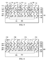
- FIGS. 2-5 illustrate the photolithography processes for forming air trenches.
- photo resist 114 is formed over package component 100 , and is then patterned.
- the portions of surface dielectric layer 110 that encircle metal pads 112 are exposed through the openings in photo resist 114 .
- the exposed portions of surface dielectric layer 110 may form rings encircling metal pads 112 in some exemplary embodiments.
- metal pads 112 are also exposed, although metal pads 112 may also be covered by the remaining photo resist 114 .
- surface dielectric layer 110 is etched, for example, using a dry etching method.
- the etchant gas may be selected to attack surface dielectric layer 110 , and not to attack metal pads 112 .
- air trenches 116 are formed to encircle metal pads 112 .
- Exemplary air trenches 116 are shown in the top view in FIG. 11 .
- the sidewalls of metal pads 112 are exposed to air trenches 116 .
- the sidewalls of metal pads 112 and the sidewalls of surface dielectric layer 110 which sidewalls are exposed to air trenches 116 , may be substantially vertical.
- Depth D1 of air trenches 116 may be equal to thickness T1 of surface dielectric layer 110 in some embodiments. Alternatively, depth D1 may be greater than or smaller than thickness T1. Width W1 of air trenches 116 may be between about 0.1 ⁇ m and about 2 ⁇ m, greater than about 0.5 ⁇ m, or between about 0.5 ⁇ m and about 2 ⁇ m. It is appreciated, however, that the values recited throughout the description are merely examples, and may be changed to different values. After the etching step, photo resist 114 is removed.
- FIGS. 4 and 5 illustrate the formation of air trench 116 in accordance with alternative embodiments. These embodiments are similar to the embodiments in FIGS. 2 and 3 , except that the outer portions of metal pads 112 , rather than portions of surface dielectric layer 110 , are etched.
- photo resist 114 is formed and patterned. The center portions of metal pads 112 are protected by portions of photo resist 114 , while the outer portions metal pads 112 are exposed.
- surface dielectric layer 110 is shown as entirely covered by photo resist 114 , the openings in photo resist 114 may also extend slightly to expose some portions of surface dielectric layer 110 to allow some process margin.
- metal pads 112 are etched to form air trenches 116 .
- the etchant gas may be selected to attack metal pads 112 , and not to attack surface dielectric layer 110 .
- Air trenches 116 may form rings encircling the remaining portions of metal pads 112 , as shown in the top view in FIG. 11 in some embodiments. As shown in FIG. 5 , the sidewalls of the remaining metal pads 112 are exposed to air trenches 116 .
- Depth D1 of air trenches 116 may be equal to thickness T2 of metal pads 112 in some embodiments. Alternatively, depth D1 may be greater than or smaller than thickness T2.
- Width W1 of air trenches 116 may be between about 0.1 ⁇ m and about 2 ⁇ m, greater than about 0.5 ⁇ m, or between about 0.5 ⁇ m and about 2 ⁇ m.
- FIG. 6 illustrates package component 200 , which is to be bonded to package component 100 .
- Package component 200 may also be selected from a device wafer, an interposer wafer, a package substrate, and the like.
- package component 200 includes substrate 202 , active devices 204 , dielectric layers 208 , metal lines and vias 206 in dielectric layers 208 , surface dielectric layer 210 , and metal pads 212 .
- Package component 200 may have a structure similar to what is described for package component 100 , and the details are not repeated herein.
- the materials of the features in package component 200 may be found referring to the like features in package component 100 , with the like features in package component 100 starting with number “1,” which features correspond to the features in package component 200 and having reference numerals starting with number “2.”
- FIGS. 6 and 7 also illustrate the formation of air trenches 216 in accordance with various embodiments. The processes are essentially the same as in FIGS. 2 and 3 , and hence some of the details may not be repeated herein.
- photo resist 214 is formed, wherein portions of surface dielectric layer 210 are exposed through the openings in photo resist 214 .
- Metal pads 212 may also be exposed, although they may be covered in alternative embodiments.
- surface dielectric layer 210 is etched, for example, using a dry etching method.
- the etchant gas may be selected to attack surface dielectric layer 210 , and not to attack metal pads 212 .
- air trenches 216 are formed to encircle metal pads 212 .
- Air trenches 216 may form rings encircling metal pads 212 , as shown in the top view in FIG. 11 .
- the sidewalls of metal pads 112 are exposed to air trenches 216 .
- Depth D2 of air trenches 216 may be equal to thickness T3 of surface dielectric layer 210 in some embodiments. Alternatively, depth D2 may be greater than or smaller than thickness T3.
- Width W2 of air trenches 116 may be essentially the same as width W1 ( FIG. 3 ).
- FIGS. 8 and 9 illustrate the etching of metal pads 212 to form air trenches 216 in accordance with alternative embodiments. These embodiments are similar to the embodiments in FIGS. 4 and 5 .
- photo resist 214 is formed and patterned. The center portions of metal pads 212 are protected by a portion of photo resist 214 , while the outer portions are exposed.
- surface dielectric layer 210 is shown as covered by photo resist 214 , the openings in photo resist 214 may also extend slightly to expose some portions of surface dielectric layer 210 to allow some process margin.
- metal pads 212 are etched to form air trenches 216 .
- the etchant gas may be selected to attack metal pads 212 , and not to attack surface dielectric layer 210 .
- Air trenches 216 may form rings encircling the remaining portions of metal pads 212 , as shown in the top view in FIG. 11 . As shown in FIG. 9 , the sidewalls of the remaining metal pads 212 are exposed to air trenches 216 .
- Depth D2 of air trenches 216 may be equal to thickness T4 of metal pads 212 in some embodiments. Alternatively, depth D2 may be greater than or smaller than thickness T4. Width W1 of air trenches 216 may be essentially the same as width W1 ( FIG. 5 ).
- package components 100 and 200 are pre-bonded.
- package components 100 and 200 are first aligned, with bond pads 112 of package component 100 aligned to bond pads 212 of package component 200 .
- package components 100 and 200 are pressed against each other.
- a small pressing force may be applied to press package components 100 and 200 against each other, which pressing force may be lower than about 5 Newton per die, for example.
- the pre-bonding may be performed at the room temperature (for example, between about 21° C. to about 25° C.), although higher temperatures may be used.
- the bonding time may be shorter than about 1 minute, for example.
- surface dielectric layer 110 and 210 are bonded to each other.
- the bonding strength needs to be improved in a subsequent annealing step.
- the bonded package components 100 and 200 may be annealed at a temperature between about 300° C. and about 400° C., for example. The annealing may be performed for a period of time between about 1 hour and 2 hours. When temperature rises, the OH bond in surface dielectric layers 110 and 210 break to form strong Si—O—Si bonds, and hence package components 100 and 200 are bonded to each other through fusion bonds (and through Van Der Waals force).
- the bonded package components 100 and 200 are sawed into packages, with the portions of package components 100 and 200 in the packages comprising dies.
- air trenches 116 and 216 may be aligned to each other, and are interconnected to form continuous air trenches extending from package component 100 into package component 200 . Furthermore, the integrated air trenches 116 and 216 encircle the bonded metal pads 112 and 212 .
- FIG. 11 illustrates a top view showing air trenches 116 and 216 are overlapped, and metal pads 112 and 212 are stacked.
- air trench trenches 116 and 216 are not necessarily filled with air.
- trenches 116 and 216 may be vacuumed, or may be filled with other types of gases such as nitrogen.
- air trenches 116 and 216 encircle bonded metal pads 112 and 212 .
- air trenches 116 and 216 do not extend into regions 18 .
- air trenches 116 and 216 may be formed on the opposite sides of metal pads 112 and 212 , and do not form rings in these embodiments.
- free spaces are generated around the bonded metal pads.
- the metal pads expand more than the surface dielectric layers since their Coefficient of Thermal Expansion (CTE) is greater than the CTE of the surface dielectric layers.
- CTE Coefficient of Thermal Expansion
- the expanded metal pads apply stresses to the surrounding dielectric layers, and hence cause damage to the fusion bonds of the surrounding dielectric layers.
- free spaces are created to allow the metal pads to expand freely without applying stresses on the surrounding dielectric layers, and hence the surrounding dielectric layers may have good fusion bonds formed.
- a package component includes a surface dielectric layer including a planar top surface, a metal pad in the surface dielectric layer and including a second planar top surface level with the planar top surface, and an air trench on a side of the metal pad. The sidewall of the metal pad is exposed to the air trench.
- a method includes performing a photo lithography process on a first package component to form an air trench in a first surface dielectric layer of the first package component.
- the air trench encircles a first metal pad in the first surface dielectric layer.
- the method further includes bonding the first package component to a second package component.
- the first metal pad is bonded to a second metal pad of the second package component.
- the first surface dielectric layer is bonded to a second surface dielectric layer of the second package component.
Landscapes
- Engineering & Computer Science (AREA)
- Manufacturing & Machinery (AREA)
- Internal Circuitry In Semiconductor Integrated Circuit Devices (AREA)
Abstract
Description
Claims (20)
Priority Applications (5)
| Application Number | Priority Date | Filing Date | Title |
|---|---|---|---|
| US13/895,122 US9443796B2 (en) | 2013-03-15 | 2013-05-15 | Air trench in packages incorporating hybrid bonding |
| US14/302,666 US9312229B2 (en) | 2013-03-15 | 2014-06-12 | Hybrid bonding with air-gap structure |
| US15/042,268 US9502396B2 (en) | 2013-03-15 | 2016-02-12 | Air trench in packages incorporating hybrid bonding |
| US15/071,576 US9960142B2 (en) | 2013-03-15 | 2016-03-16 | Hybrid bonding with air-gap structure |
| US15/356,887 US9786628B2 (en) | 2013-03-15 | 2016-11-21 | Air trench in packages incorporating hybrid bonding |
Applications Claiming Priority (2)
| Application Number | Priority Date | Filing Date | Title |
|---|---|---|---|
| US201361793355P | 2013-03-15 | 2013-03-15 | |
| US13/895,122 US9443796B2 (en) | 2013-03-15 | 2013-05-15 | Air trench in packages incorporating hybrid bonding |
Related Child Applications (2)
| Application Number | Title | Priority Date | Filing Date |
|---|---|---|---|
| US15/042,268 Division US9502396B2 (en) | 2013-03-15 | 2016-02-12 | Air trench in packages incorporating hybrid bonding |
| US15/042,268 Continuation US9502396B2 (en) | 2013-03-15 | 2016-02-12 | Air trench in packages incorporating hybrid bonding |
Publications (2)
| Publication Number | Publication Date |
|---|---|
| US20140264948A1 US20140264948A1 (en) | 2014-09-18 |
| US9443796B2 true US9443796B2 (en) | 2016-09-13 |
Family
ID=51523965
Family Applications (5)
| Application Number | Title | Priority Date | Filing Date |
|---|---|---|---|
| US13/895,122 Expired - Fee Related US9443796B2 (en) | 2013-03-15 | 2013-05-15 | Air trench in packages incorporating hybrid bonding |
| US14/302,666 Active US9312229B2 (en) | 2013-03-15 | 2014-06-12 | Hybrid bonding with air-gap structure |
| US15/042,268 Expired - Fee Related US9502396B2 (en) | 2013-03-15 | 2016-02-12 | Air trench in packages incorporating hybrid bonding |
| US15/071,576 Active US9960142B2 (en) | 2013-03-15 | 2016-03-16 | Hybrid bonding with air-gap structure |
| US15/356,887 Active US9786628B2 (en) | 2013-03-15 | 2016-11-21 | Air trench in packages incorporating hybrid bonding |
Family Applications After (4)
| Application Number | Title | Priority Date | Filing Date |
|---|---|---|---|
| US14/302,666 Active US9312229B2 (en) | 2013-03-15 | 2014-06-12 | Hybrid bonding with air-gap structure |
| US15/042,268 Expired - Fee Related US9502396B2 (en) | 2013-03-15 | 2016-02-12 | Air trench in packages incorporating hybrid bonding |
| US15/071,576 Active US9960142B2 (en) | 2013-03-15 | 2016-03-16 | Hybrid bonding with air-gap structure |
| US15/356,887 Active US9786628B2 (en) | 2013-03-15 | 2016-11-21 | Air trench in packages incorporating hybrid bonding |
Country Status (1)
| Country | Link |
|---|---|
| US (5) | US9443796B2 (en) |
Cited By (110)
| Publication number | Priority date | Publication date | Assignee | Title |
|---|---|---|---|---|
| US20170069593A1 (en) * | 2013-03-15 | 2017-03-09 | Taiwan Semiconductor Manufacturing Company, Ltd. | Air Trench in Packages Incorporating Hybrid Bonding |
| US10508030B2 (en) | 2017-03-21 | 2019-12-17 | Invensas Bonding Technologies, Inc. | Seal for microelectronic assembly |
| US10515913B2 (en) | 2017-03-17 | 2019-12-24 | Invensas Bonding Technologies, Inc. | Multi-metal contact structure |
| US10515925B2 (en) | 2017-04-21 | 2019-12-24 | Invensas Bonding Technologies, Inc. | Die processing |
| US10522499B2 (en) | 2017-02-09 | 2019-12-31 | Invensas Bonding Technologies, Inc. | Bonded structures |
| US10529634B2 (en) | 2017-05-11 | 2020-01-07 | Invensas Bonding Technologies, Inc. | Probe methodology for ultrafine pitch interconnects |
| US10546832B2 (en) | 2016-12-21 | 2020-01-28 | Invensas Bonding Technologies, Inc. | Bonded structures |
| US10607937B2 (en) | 2015-12-18 | 2020-03-31 | Invensas Bonding Technologies, Inc. | Increased contact alignment tolerance for direct bonding |
| US10658313B2 (en) | 2017-12-11 | 2020-05-19 | Invensas Bonding Technologies, Inc. | Selective recess |
| US10727219B2 (en) | 2018-02-15 | 2020-07-28 | Invensas Bonding Technologies, Inc. | Techniques for processing devices |
| US10777533B2 (en) | 2012-08-30 | 2020-09-15 | Invensas Bonding Technologies, Inc. | Heterogeneous device |
| US10784191B2 (en) | 2017-03-31 | 2020-09-22 | Invensas Bonding Technologies, Inc. | Interface structures and methods for forming same |
| US10790262B2 (en) | 2018-04-11 | 2020-09-29 | Invensas Bonding Technologies, Inc. | Low temperature bonded structures |
| US10796936B2 (en) | 2016-12-22 | 2020-10-06 | Invensas Bonding Technologies, Inc. | Die tray with channels |
| US10840205B2 (en) | 2017-09-24 | 2020-11-17 | Invensas Bonding Technologies, Inc. | Chemical mechanical polishing for hybrid bonding |
| US10879226B2 (en) | 2016-05-19 | 2020-12-29 | Invensas Bonding Technologies, Inc. | Stacked dies and methods for forming bonded structures |
| US10879212B2 (en) | 2017-05-11 | 2020-12-29 | Invensas Bonding Technologies, Inc. | Processed stacked dies |
| US10896902B2 (en) | 2016-01-13 | 2021-01-19 | Invensas Bonding Technologies, Inc. | Systems and methods for efficient transfer of semiconductor elements |
| US10923408B2 (en) | 2017-12-22 | 2021-02-16 | Invensas Bonding Technologies, Inc. | Cavity packages |
| US10964664B2 (en) | 2018-04-20 | 2021-03-30 | Invensas Bonding Technologies, Inc. | DBI to Si bonding for simplified handle wafer |
| US10998265B2 (en) | 2016-09-30 | 2021-05-04 | Invensas Bonding Technologies, Inc. | Interface structures and methods for forming same |
| US10998292B2 (en) | 2018-06-13 | 2021-05-04 | Invensas Bonding Technologies, Inc. | Offset pads over TSV |
| US11004757B2 (en) | 2018-05-14 | 2021-05-11 | Invensas Bonding Technologies, Inc. | Bonded structures |
| US11011503B2 (en) | 2017-12-15 | 2021-05-18 | Invensas Bonding Technologies, Inc. | Direct-bonded optoelectronic interconnect for high-density integrated photonics |
| US11011491B2 (en) | 2019-09-06 | 2021-05-18 | Advanced Semiconductor Engineering, Inc. | Semiconductor device packages and methods of manufacturing the same |
| US11011494B2 (en) | 2018-08-31 | 2021-05-18 | Invensas Bonding Technologies, Inc. | Layer structures for making direct metal-to-metal bonds at low temperatures in microelectronics |
| US11011418B2 (en) | 2005-08-11 | 2021-05-18 | Invensas Bonding Technologies, Inc. | 3D IC method and device |
| US11031285B2 (en) | 2017-10-06 | 2021-06-08 | Invensas Bonding Technologies, Inc. | Diffusion barrier collar for interconnects |
| US11056348B2 (en) | 2018-04-05 | 2021-07-06 | Invensas Bonding Technologies, Inc. | Bonding surfaces for microelectronics |
| US11056390B2 (en) | 2015-06-24 | 2021-07-06 | Invensas Corporation | Structures and methods for reliable packages |
| US11158573B2 (en) | 2018-10-22 | 2021-10-26 | Invensas Bonding Technologies, Inc. | Interconnect structures |
| US11158606B2 (en) | 2018-07-06 | 2021-10-26 | Invensas Bonding Technologies, Inc. | Molded direct bonded and interconnected stack |
| US11169326B2 (en) | 2018-02-26 | 2021-11-09 | Invensas Bonding Technologies, Inc. | Integrated optical waveguides, direct-bonded waveguide interface joints, optical routing and interconnects |
| US11171117B2 (en) | 2018-06-12 | 2021-11-09 | Invensas Bonding Technologies, Inc. | Interlayer connection of stacked microelectronic components |
| US11195748B2 (en) | 2017-09-27 | 2021-12-07 | Invensas Corporation | Interconnect structures and methods for forming same |
| US11205600B2 (en) | 2014-03-12 | 2021-12-21 | Invensas Corporation | Integrated circuits protected by substrates with cavities, and methods of manufacture |
| US11205625B2 (en) | 2019-04-12 | 2021-12-21 | Invensas Bonding Technologies, Inc. | Wafer-level bonding of obstructive elements |
| US11244928B2 (en) | 2020-03-12 | 2022-02-08 | SK Hynix Inc. | Stacked type semiconductor device including through electrode |
| US11244920B2 (en) | 2018-12-18 | 2022-02-08 | Invensas Bonding Technologies, Inc. | Method and structures for low temperature device bonding |
| US11244916B2 (en) | 2018-04-11 | 2022-02-08 | Invensas Bonding Technologies, Inc. | Low temperature bonded structures |
| US11256004B2 (en) | 2018-03-20 | 2022-02-22 | Invensas Bonding Technologies, Inc. | Direct-bonded lamination for improved image clarity in optical devices |
| US11264345B2 (en) | 2015-08-25 | 2022-03-01 | Invensas Bonding Technologies, Inc. | Conductive barrier direct hybrid bonding |
| US11276676B2 (en) | 2018-05-15 | 2022-03-15 | Invensas Bonding Technologies, Inc. | Stacked devices and methods of fabrication |
| US11296044B2 (en) | 2018-08-29 | 2022-04-05 | Invensas Bonding Technologies, Inc. | Bond enhancement structure in microelectronics for trapping contaminants during direct-bonding processes |
| US11296053B2 (en) | 2019-06-26 | 2022-04-05 | Invensas Bonding Technologies, Inc. | Direct bonded stack structures for increased reliability and improved yield in microelectronics |
| US11348801B2 (en) | 2016-12-28 | 2022-05-31 | Invensas Bonding Technologies, Inc. | Processing stacked substrates |
| US11355404B2 (en) | 2019-04-22 | 2022-06-07 | Invensas Bonding Technologies, Inc. | Mitigating surface damage of probe pads in preparation for direct bonding of a substrate |
| US11367652B2 (en) | 2016-12-28 | 2022-06-21 | Invensas Bonding Technologies, Inc. | Microelectronic assembly from processed substrate |
| US11373963B2 (en) | 2019-04-12 | 2022-06-28 | Invensas Bonding Technologies, Inc. | Protective elements for bonded structures |
| US11380597B2 (en) | 2017-12-22 | 2022-07-05 | Invensas Bonding Technologies, Inc. | Bonded structures |
| US11385278B2 (en) | 2019-05-23 | 2022-07-12 | Invensas Bonding Technologies, Inc. | Security circuitry for bonded structures |
| US11387214B2 (en) | 2017-06-15 | 2022-07-12 | Invensas Llc | Multi-chip modules formed using wafer-level processing of a reconstituted wafer |
| US11393779B2 (en) | 2018-06-13 | 2022-07-19 | Invensas Bonding Technologies, Inc. | Large metal pads over TSV |
| US11462419B2 (en) | 2018-07-06 | 2022-10-04 | Invensas Bonding Technologies, Inc. | Microelectronic assemblies |
| US11476213B2 (en) | 2019-01-14 | 2022-10-18 | Invensas Bonding Technologies, Inc. | Bonded structures without intervening adhesive |
| US11515291B2 (en) | 2018-08-28 | 2022-11-29 | Adeia Semiconductor Inc. | Integrated voltage regulator and passive components |
| US11538781B2 (en) | 2020-06-30 | 2022-12-27 | Adeia Semiconductor Bonding Technologies Inc. | Integrated device packages including bonded structures |
| US11610846B2 (en) | 2019-04-12 | 2023-03-21 | Adeia Semiconductor Bonding Technologies Inc. | Protective elements for bonded structures including an obstructive element |
| US11621246B2 (en) | 2019-03-29 | 2023-04-04 | Adeia Semiconductor Technologies Llc | Diffused bitline replacement in stacked wafer memory |
| US11626363B2 (en) | 2016-12-29 | 2023-04-11 | Adeia Semiconductor Bonding Technologies Inc. | Bonded structures with integrated passive component |
| US11664357B2 (en) | 2018-07-03 | 2023-05-30 | Adeia Semiconductor Bonding Technologies Inc. | Techniques for joining dissimilar materials in microelectronics |
| US11710718B2 (en) | 2015-07-10 | 2023-07-25 | Adeia Semiconductor Technologies Llc | Structures and methods for low temperature bonding using nanoparticles |
| US11715730B2 (en) | 2017-03-16 | 2023-08-01 | Adeia Semiconductor Technologies Llc | Direct-bonded LED arrays including optical elements configured to transmit optical signals from LED elements |
| US11721653B2 (en) | 2019-12-23 | 2023-08-08 | Adeia Semiconductor Bonding Technologies Inc. | Circuitry for electrical redundancy in bonded structures |
| US11728273B2 (en) | 2020-09-04 | 2023-08-15 | Adeia Semiconductor Bonding Technologies Inc. | Bonded structure with interconnect structure |
| US11735523B2 (en) | 2020-05-19 | 2023-08-22 | Adeia Semiconductor Bonding Technologies Inc. | Laterally unconfined structure |
| US11742314B2 (en) | 2020-03-31 | 2023-08-29 | Adeia Semiconductor Bonding Technologies Inc. | Reliable hybrid bonded apparatus |
| US11762200B2 (en) | 2019-12-17 | 2023-09-19 | Adeia Semiconductor Bonding Technologies Inc. | Bonded optical devices |
| US11760059B2 (en) | 2003-05-19 | 2023-09-19 | Adeia Semiconductor Bonding Technologies Inc. | Method of room temperature covalent bonding |
| US11764177B2 (en) | 2020-09-04 | 2023-09-19 | Adeia Semiconductor Bonding Technologies Inc. | Bonded structure with interconnect structure |
| US11842894B2 (en) | 2019-12-23 | 2023-12-12 | Adeia Semiconductor Bonding Technologies Inc. | Electrical redundancy for bonded structures |
| US11862604B2 (en) | 2018-06-22 | 2024-01-02 | Adeia Semiconductor Inc. | Systems and methods for releveled bump planes for chiplets |
| US11862602B2 (en) | 2019-11-07 | 2024-01-02 | Adeia Semiconductor Technologies Llc | Scalable architecture for reduced cycles across SOC |
| US11876076B2 (en) | 2019-12-20 | 2024-01-16 | Adeia Semiconductor Technologies Llc | Apparatus for non-volatile random access memory stacks |
| US11881454B2 (en) | 2016-10-07 | 2024-01-23 | Adeia Semiconductor Inc. | Stacked IC structure with orthogonal interconnect layers |
| US11901281B2 (en) | 2019-03-11 | 2024-02-13 | Adeia Semiconductor Bonding Technologies Inc. | Bonded structures with integrated passive component |
| US11908739B2 (en) | 2017-06-05 | 2024-02-20 | Adeia Semiconductor Technologies Llc | Flat metal features for microelectronics applications |
| US11929347B2 (en) | 2020-10-20 | 2024-03-12 | Adeia Semiconductor Technologies Llc | Mixed exposure for large die |
| US11935907B2 (en) | 2014-12-11 | 2024-03-19 | Adeia Semiconductor Technologies Llc | Image sensor device |
| US11973056B2 (en) | 2016-10-27 | 2024-04-30 | Adeia Semiconductor Technologies Llc | Methods for low temperature bonding using nanoparticles |
| US12009338B2 (en) | 2020-03-19 | 2024-06-11 | Adeia Semiconductor Bonding Technologies Inc. | Dimension compensation control for directly bonded structures |
| US12074092B2 (en) | 2018-05-30 | 2024-08-27 | Adeia Semiconductor Inc. | Hard IP blocks with physically bidirectional passageways |
| US12080672B2 (en) | 2019-09-26 | 2024-09-03 | Adeia Semiconductor Bonding Technologies Inc. | Direct gang bonding methods including directly bonding first element to second element to form bonded structure without adhesive |
| US20240312940A1 (en) * | 2023-03-17 | 2024-09-19 | Taiwan Semiconductor Manufacturing Company, Ltd. | Semiconductor device and method for manufacturing the same |
| US12113054B2 (en) | 2019-10-21 | 2024-10-08 | Adeia Semiconductor Technologies Llc | Non-volatile dynamic random access memory |
| US12142528B2 (en) | 2016-10-07 | 2024-11-12 | Adeia Semiconductor Inc. | 3D chip with shared clock distribution network |
| US12191267B2 (en) | 2019-03-01 | 2025-01-07 | Adeia Semiconductor Technologies, LLC | Nanowire bonding interconnect for fine-pitch microelectronics |
| US12211809B2 (en) | 2020-12-30 | 2025-01-28 | Adeia Semiconductor Bonding Technologies Inc. | Structure with conductive feature and method of forming same |
| US12248869B2 (en) | 2017-08-03 | 2025-03-11 | Adeia Semiconductor Inc. | Three dimensional circuit implementing machine trained network |
| US12272730B2 (en) | 2018-03-29 | 2025-04-08 | Adeia Semiconductor Inc. | Transistor level interconnection methodologies utilizing 3D interconnects |
| US12300634B2 (en) | 2021-08-02 | 2025-05-13 | Adeia Semiconductor Bonding Technologies Inc. | Protective semiconductor elements for bonded structures |
| US12341083B2 (en) | 2023-02-08 | 2025-06-24 | Adeia Semiconductor Bonding Technologies Inc. | Electronic device cooling structures bonded to semiconductor elements |
| US12374641B2 (en) | 2019-06-12 | 2025-07-29 | Adeia Semiconductor Bonding Technologies Inc. | Sealed bonded structures and methods for forming the same |
| US12381128B2 (en) | 2020-12-28 | 2025-08-05 | Adeia Semiconductor Bonding Technologies Inc. | Structures with through-substrate vias and methods for forming the same |
| US12406959B2 (en) | 2018-07-26 | 2025-09-02 | Adeia Semiconductor Bonding Technologies Inc. | Post CMP processing for hybrid bonding |
| US12424584B2 (en) | 2020-10-29 | 2025-09-23 | Adeia Semiconductor Bonding Technologies Inc. | Direct bonding methods and structures |
| US12456662B2 (en) | 2020-12-28 | 2025-10-28 | Adeia Semiconductor Bonding Technologies Inc. | Structures with through-substrate vias and methods for forming the same |
| US12506114B2 (en) | 2022-12-29 | 2025-12-23 | Adeia Semiconductor Bonding Technologies Inc. | Directly bonded metal structures having aluminum features and methods of preparing same |
| US12512425B2 (en) | 2022-04-25 | 2025-12-30 | Adeia Semiconductor Bonding Technologies Inc. | Expansion controlled structure for direct bonding and method of forming same |
| US12525572B2 (en) | 2021-03-31 | 2026-01-13 | Adeia Semiconductor Bonding Technologies Inc. | Direct bonding and debonding of carrier |
| US12543577B2 (en) | 2021-09-24 | 2026-02-03 | Adeia Semiconductor Bonding Technologies Inc. | Bonded structure with active interposer |
| US12543568B2 (en) | 2021-12-20 | 2026-02-03 | Adeia Semiconductor Bonding Technologies Inc. | Thermoelectric cooling for die packages |
| US12545010B2 (en) | 2022-12-29 | 2026-02-10 | Adeia Semiconductor Bonding Technologies Inc. | Directly bonded metal structures having oxide layers therein |
| US12550799B2 (en) | 2021-03-31 | 2026-02-10 | Adeia Semiconductor Bonding Technologies Inc. | Direct bonding methods and structures |
| US12557615B2 (en) | 2021-12-13 | 2026-02-17 | Adeia Semiconductor Technologies Llc | Methods for bonding semiconductor elements |
| US12563749B2 (en) | 2021-10-28 | 2026-02-24 | Adeia Semiconductor Bonding Technologies Inc | Stacked electronic devices |
| US12591005B2 (en) | 2022-05-23 | 2026-03-31 | Adeia Semiconductor Bonding Technologies Inc. | Testing elements for bonded structures |
| US12598962B2 (en) | 2023-03-14 | 2026-04-07 | Adeia Semiconductor Bonding Technologies Inc. | System and method for bonding transparent conductor substrates |
| US12604771B2 (en) | 2021-10-28 | 2026-04-14 | Adeia Semiconductor Bonding Technologies Inc. | Direct bonding methods and structures |
| US12622307B2 (en) | 2022-12-21 | 2026-05-05 | Adeia Semiconductor Bonding Technologies Inc. | Controlled grain growth for bonding and bonded structure with controlled grain growth |
Families Citing this family (61)
| Publication number | Priority date | Publication date | Assignee | Title |
|---|---|---|---|---|
| CN104126220B (en) * | 2011-12-20 | 2017-06-20 | 英特尔公司 | Conformal Low Temperature Hermetic Dielectric Diffusion Barriers |
| US9524950B2 (en) | 2013-05-31 | 2016-12-20 | Freescale Semiconductor, Inc. | Stacked microelectronic packages having sidewall conductors and methods for the fabrication thereof |
| WO2015040784A1 (en) * | 2013-09-17 | 2015-03-26 | パナソニックIpマネジメント株式会社 | Semiconductor device and method for manufacturing same |
| US9263420B2 (en) * | 2013-12-05 | 2016-02-16 | Freescale Semiconductor, Inc. | Devices and stacked microelectronic packages with package surface conductors and methods of their fabrication |
| US9349690B2 (en) * | 2014-03-13 | 2016-05-24 | Taiwan Semiconductor Manufacturing Company Limited | Semiconductor arrangement and formation thereof |
| US10388607B2 (en) | 2014-12-17 | 2019-08-20 | Nxp Usa, Inc. | Microelectronic devices with multi-layer package surface conductors and methods of their fabrication |
| US9941241B2 (en) * | 2016-06-30 | 2018-04-10 | International Business Machines Corporation | Method for wafer-wafer bonding |
| US10276909B2 (en) | 2016-12-30 | 2019-04-30 | Invensas Bonding Technologies, Inc. | Structure comprising at least a first element bonded to a carrier having a closed metallic channel waveguide formed therein |
| US10854568B2 (en) * | 2017-04-07 | 2020-12-01 | Taiwan Semiconductor Manufacturing Company, Ltd. | Packages with Si-substrate-free interposer and method forming same |
| DE102017124104B4 (en) | 2017-04-07 | 2025-05-15 | Taiwan Semiconductor Manufacturing Co., Ltd. | Packages with Si-substrate-free interposer and methods for forming the same |
| US10522449B2 (en) | 2017-04-10 | 2019-12-31 | Taiwan Semiconductor Manufacturing Company, Ltd. | Packages with Si-substrate-free interposer and method forming same |
| DE102017123449B4 (en) | 2017-04-10 | 2023-12-28 | Taiwan Semiconductor Manufacturing Co. Ltd. | Housing with Si-substrate-free intermediate piece and training process |
| CN107256852B (en) * | 2017-06-20 | 2019-09-13 | 上海集成电路研发中心有限公司 | Metal bonding point array with improved arrangement and semiconductor device having the same |
| CN112164688B (en) * | 2017-07-21 | 2023-06-13 | 联华电子股份有限公司 | Chip stacking structure and manufacturing method of chip stacking structure |
| US10290611B2 (en) * | 2017-07-27 | 2019-05-14 | Taiwan Semiconductor Manufacturing Company, Ltd. | Semiconductor packages and methods of forming same |
| JP2019047043A (en) * | 2017-09-05 | 2019-03-22 | 日本放送協会 | Stacked semiconductor device, semiconductor device substrate, and manufacturing method thereof |
| US10290571B2 (en) | 2017-09-18 | 2019-05-14 | Taiwan Semiconductor Manufacturing Company, Ltd. | Packages with si-substrate-free interposer and method forming same |
| US10685935B2 (en) * | 2017-11-15 | 2020-06-16 | Taiwan Semiconductor Manufacturing Company, Ltd. | Forming metal bonds with recesses |
| US10535636B2 (en) * | 2017-11-15 | 2020-01-14 | Taiwan Semiconductor Manufacturing Company, Ltd. | Integrating passive devices in package structures |
| US10672820B2 (en) * | 2017-11-23 | 2020-06-02 | Taiwan Semiconductor Manufacturing Co., Ltd. | Hybrid bonded structure |
| DE102018112586B4 (en) * | 2018-05-25 | 2025-12-04 | OSRAM Opto Semiconductors Gesellschaft mit beschränkter Haftung | METHOD FOR CREATING A CONNECTION BETWEEN COMPONENTS AND BUILDING ELEMENT |
| WO2020000380A1 (en) * | 2018-06-29 | 2020-01-02 | 长江存储科技有限责任公司 | Semiconductor structure and forming method therefor |
| WO2020000376A1 (en) * | 2018-06-29 | 2020-01-02 | 长江存储科技有限责任公司 | Semiconductor structure and forming method therefor |
| CN112567512B (en) * | 2018-06-29 | 2023-09-01 | 长江存储科技有限责任公司 | Semiconductor structures and methods of forming them |
| CN110858578B (en) * | 2018-08-23 | 2021-07-13 | 联华电子股份有限公司 | Die seal ring and method of making the same |
| US10861808B2 (en) * | 2018-11-21 | 2020-12-08 | Taiwan Semiconductor Manufacturing Company, Ltd. | Bonding structure of dies with dangling bonds |
| DE102019109844B4 (en) | 2018-11-21 | 2025-03-20 | Taiwan Semiconductor Manufacturing Co., Ltd. | Bond structure of this product with hanging bonds and method for producing the same |
| TWI680511B (en) * | 2018-11-23 | 2019-12-21 | 南亞科技股份有限公司 | Semiconductor structure and manufacturing method thereof |
| US10734338B2 (en) * | 2018-11-23 | 2020-08-04 | Nanya Technology Corporation | Bonding pad, semiconductor structure, and method of manufacturing semiconductor structure |
| WO2020154939A1 (en) * | 2019-01-30 | 2020-08-06 | Yangtze Memory Technologies Co., Ltd. | Hybrid bonding using dummy bonding contacts |
| CN109964313A (en) * | 2019-02-11 | 2019-07-02 | 长江存储科技有限责任公司 | Bonded semiconductor structure with bonding contacts made of non-diffused conductive material and method of forming the same |
| JP2020150232A (en) * | 2019-03-15 | 2020-09-17 | キオクシア株式会社 | Semiconductor devices and their manufacturing methods |
| US10840190B1 (en) * | 2019-05-16 | 2020-11-17 | Taiwan Semiconductor Manufacturing Company, Ltd. | Semiconductor structure and manufacturing method thereof |
| US10770424B1 (en) * | 2019-08-13 | 2020-09-08 | Nanya Technology Corporation | Semiconductor structure and method of manufacturing thereof |
| KR102744178B1 (en) | 2019-08-19 | 2024-12-19 | 삼성전자주식회사 | Semiconductor devices |
| KR102780353B1 (en) | 2019-08-26 | 2025-03-12 | 삼성전자주식회사 | Semiconductor device and method of manufacturing the same |
| US11456328B2 (en) | 2019-10-09 | 2022-09-27 | Omnivision Technologies, Inc. | Stack chip air gap heat insulator |
| US11011486B1 (en) | 2019-11-05 | 2021-05-18 | United Microelectronics Corp. | Bonded semiconductor structure and method for forming the same |
| US11088076B2 (en) * | 2019-12-27 | 2021-08-10 | Sandisk Technologies Llc | Bonding pads embedded in a dielectric diffusion barrier and having recessed metallic liners |
| US11257694B2 (en) * | 2020-02-04 | 2022-02-22 | Nanya Technology Corporation | Semiconductor device having hybrid bonding interface, method of manufacturing the semiconductor device, and method of manufacturing semiconductor device assembly |
| US11309249B2 (en) * | 2020-05-04 | 2022-04-19 | Nanya Technology Corporation | Semiconductor package with air gap and manufacturing method thereof |
| US11309266B2 (en) * | 2020-05-28 | 2022-04-19 | Nanya Technology Corporation | Semiconductor device structure with air gap and method for forming the same |
| KR102822691B1 (en) | 2020-06-05 | 2025-06-20 | 삼성전자주식회사 | Semiconductor device and semiconductor package including same |
| TWI755034B (en) * | 2020-08-19 | 2022-02-11 | 友達光電股份有限公司 | Device substrate and manufacturing method thereof |
| US11594506B2 (en) * | 2020-09-23 | 2023-02-28 | Advanced Semiconductor Engineering, Inc. | Semiconductor package |
| US12131951B2 (en) * | 2020-10-22 | 2024-10-29 | Changxin Memory Technologies, Inc. | Semiconductor packaging method and semiconductor structure |
| US11710712B2 (en) * | 2021-01-05 | 2023-07-25 | Taiwan Semiconductor Manufacturing Company Ltd. | Semiconductor device and manufacturing method of the same |
| CN114743942B (en) * | 2021-01-07 | 2026-02-10 | 联华电子股份有限公司 | Hybrid Joint Structure and its Manufacturing Method |
| WO2022201530A1 (en) * | 2021-03-26 | 2022-09-29 | 昭和電工マテリアルズ株式会社 | Semiconductor device production method, semiconductor device, integrated circuit element, and integrated circuit element production method |
| US12015010B2 (en) * | 2021-03-31 | 2024-06-18 | Taiwan Semiconductor Manufacturing Company Limited | Vertically stacked semiconductor device including a hybrid bond contact junction circuit and methods of forming the same |
| FR3121544B1 (en) * | 2021-03-31 | 2023-11-24 | St Microelectronics Crolles 2 Sas | Thermal and electrical insulation structure |
| CN115565977B (en) | 2021-07-01 | 2024-06-07 | 长鑫存储技术有限公司 | Semiconductor structure and manufacturing method thereof |
| US11948902B2 (en) * | 2021-07-08 | 2024-04-02 | Sandisk Technologies Llc | Bonded assembly including an airgap containing bonding-level dielectric layer and methods of forming the same |
| US11817420B2 (en) * | 2021-07-19 | 2023-11-14 | Micron Technology, Inc. | Systems and methods for direct bonding in semiconductor die manufacturing |
| JP2024538179A (en) * | 2021-10-18 | 2024-10-18 | アデイア セミコンダクター テクノロジーズ リミテッド ライアビリティ カンパニー | Reducing parasitic capacitance in coupling structures |
| KR20230068590A (en) | 2021-11-11 | 2023-05-18 | 삼성전자주식회사 | Semiconductor package, and method of manufacturing the same |
| US12593711B2 (en) * | 2022-06-30 | 2026-03-31 | Taiwan Semiconductor Manufacturing Company, Ltd. | Bonding structure with stress buffer zone and method of forming same |
| KR20240015225A (en) | 2022-07-26 | 2024-02-05 | 삼성전자주식회사 | Semiconductor package |
| CN116454050B (en) * | 2023-03-09 | 2025-02-07 | 长鑫存储技术有限公司 | Semiconductor packaging structure and method for forming the same |
| KR20240139871A (en) * | 2023-03-15 | 2024-09-24 | 삼성전자주식회사 | Bonding semiconductor device, and chip for bonding semiconductor device and method of manufacturing the same |
| US20250167041A1 (en) * | 2023-11-21 | 2025-05-22 | Stmicroelectronics International N.V. | Beol integration solution based on direct cmp to improve intermetal dielectric layer |
Citations (19)
| Publication number | Priority date | Publication date | Assignee | Title |
|---|---|---|---|---|
| US6307755B1 (en) | 1999-05-27 | 2001-10-23 | Richard K. Williams | Surface mount semiconductor package, die-leadframe combination and leadframe therefor and method of mounting leadframes to surfaces of semiconductor die |
| US20020163072A1 (en) | 2001-05-01 | 2002-11-07 | Subhash Gupta | Method for bonding wafers to produce stacked integrated circuits |
| US20030193076A1 (en) | 2002-04-11 | 2003-10-16 | Robert Patti | Interlocking conductor method for bonding wafers to produce stacked integrated circuits |
| US20050161795A1 (en) * | 2003-02-07 | 2005-07-28 | Ziptronix | Room temperature metal direct bonding |
| US20080006938A1 (en) | 2006-07-10 | 2008-01-10 | Robert Patti | Method for bonding wafers to produce stacked integrated circuits |
| US20100258890A1 (en) | 2009-04-10 | 2010-10-14 | Siliconfile Technologies Inc. | Unit pixel of image sensor having three-dimensional structure and method for manufacturing the same |
| US20110084403A1 (en) | 2009-10-08 | 2011-04-14 | International Business Machines Corporation | Pad bonding employing a self-aligned plated liner for adhesion enhancement |
| US8053277B2 (en) * | 2006-12-19 | 2011-11-08 | Taiwan Semiconductor Manufacturing Company, Ltd. | Three-dimensional integrated circuits with protection layers |
| US20120094469A1 (en) | 2010-10-14 | 2012-04-19 | Didier Landru | Process for realising a connecting structure |
| US20130009321A1 (en) | 2011-07-05 | 2013-01-10 | Sony Corporation | Semiconductor device, fabrication method for a semiconductor device and electronic apparatus |
| US20130020704A1 (en) | 2011-07-18 | 2013-01-24 | S.O.I.Tec Silicon On Insulator Technologies | Bonding surfaces for direct bonding of semiconductor structures |
| US20130207268A1 (en) | 2012-02-14 | 2013-08-15 | Stmicroelectronics (Crolles 2) Sas | Chip assembly system |
| US8525354B2 (en) * | 2011-10-13 | 2013-09-03 | United Microelectronics Corporation | Bond pad structure and fabricating method thereof |
| US20130320556A1 (en) | 2012-06-05 | 2013-12-05 | Taiwan Semiconductor Manufacturing Company, Ltd. | Three Dimensional Integrated Circuit Structures and Hybrid Bonding Methods for Semiconductor Wafers |
| US20140015088A1 (en) | 2012-07-12 | 2014-01-16 | Stmicroelectronics (Crolles 2) Sas | Three-dimensional integrated structure capable of detecting a temperature rise |
| US20140117546A1 (en) | 2012-06-05 | 2014-05-01 | Taiwan Semiconductor Manufacturing Company, Ltd. | Hybrid bonding mechanisms for semiconductor wafers |
| US20140175614A1 (en) | 2012-12-20 | 2014-06-26 | Industrial Technology Research Institute | Wafer stacking structure and method of manufacturing the same |
| US20140175655A1 (en) | 2012-12-22 | 2014-06-26 | Industrial Technology Research Institute | Chip bonding structure and manufacturing method thereof |
| US8802538B1 (en) | 2013-03-15 | 2014-08-12 | Taiwan Semiconductor Manufacturing Company, Ltd. | Methods for hybrid wafer bonding |
Family Cites Families (11)
| Publication number | Priority date | Publication date | Assignee | Title |
|---|---|---|---|---|
| US5911887A (en) * | 1996-07-19 | 1999-06-15 | Cypress Semiconductor Corporation | Method of etching a bond pad |
| US6638863B2 (en) * | 2001-04-24 | 2003-10-28 | Acm Research, Inc. | Electropolishing metal layers on wafers having trenches or vias with dummy structures |
| JP2004363524A (en) * | 2003-06-09 | 2004-12-24 | Matsushita Electric Ind Co Ltd | Method of forming embedded wiring and semiconductor device |
| KR100641362B1 (en) * | 2005-01-13 | 2006-10-31 | 삼성전자주식회사 | Wiring structure with double diffusion barrier and manufacturing method |
| TW200634983A (en) * | 2005-03-18 | 2006-10-01 | United Microelectronics Corp | Method of forming a plug |
| JP5013732B2 (en) * | 2006-04-03 | 2012-08-29 | Jsr株式会社 | Chemical mechanical polishing aqueous dispersion, chemical mechanical polishing method, chemical mechanical polishing kit, and kit for preparing chemical mechanical polishing aqueous dispersion |
| JP2009158810A (en) * | 2007-12-27 | 2009-07-16 | Toshiba Corp | Chemical mechanical polishing slurry and semiconductor device manufacturing method |
| JP2010010449A (en) * | 2008-06-27 | 2010-01-14 | Toshiba Corp | Method of manufacturing semiconductor device |
| EP2597677B1 (en) * | 2011-11-23 | 2014-08-06 | ams AG | Semiconductor device with through-substrate via covered by a solder ball and related method of production |
| US9443796B2 (en) * | 2013-03-15 | 2016-09-13 | Taiwan Semiconductor Manufacturing Company, Ltd. | Air trench in packages incorporating hybrid bonding |
| US9716066B2 (en) * | 2013-06-29 | 2017-07-25 | Intel Corporation | Interconnect structure comprising fine pitch backside metal redistribution lines combined with vias |
-
2013
- 2013-05-15 US US13/895,122 patent/US9443796B2/en not_active Expired - Fee Related
-
2014
- 2014-06-12 US US14/302,666 patent/US9312229B2/en active Active
-
2016
- 2016-02-12 US US15/042,268 patent/US9502396B2/en not_active Expired - Fee Related
- 2016-03-16 US US15/071,576 patent/US9960142B2/en active Active
- 2016-11-21 US US15/356,887 patent/US9786628B2/en active Active
Patent Citations (19)
| Publication number | Priority date | Publication date | Assignee | Title |
|---|---|---|---|---|
| US6307755B1 (en) | 1999-05-27 | 2001-10-23 | Richard K. Williams | Surface mount semiconductor package, die-leadframe combination and leadframe therefor and method of mounting leadframes to surfaces of semiconductor die |
| US20020163072A1 (en) | 2001-05-01 | 2002-11-07 | Subhash Gupta | Method for bonding wafers to produce stacked integrated circuits |
| US20030193076A1 (en) | 2002-04-11 | 2003-10-16 | Robert Patti | Interlocking conductor method for bonding wafers to produce stacked integrated circuits |
| US20050161795A1 (en) * | 2003-02-07 | 2005-07-28 | Ziptronix | Room temperature metal direct bonding |
| US20080006938A1 (en) | 2006-07-10 | 2008-01-10 | Robert Patti | Method for bonding wafers to produce stacked integrated circuits |
| US8053277B2 (en) * | 2006-12-19 | 2011-11-08 | Taiwan Semiconductor Manufacturing Company, Ltd. | Three-dimensional integrated circuits with protection layers |
| US20100258890A1 (en) | 2009-04-10 | 2010-10-14 | Siliconfile Technologies Inc. | Unit pixel of image sensor having three-dimensional structure and method for manufacturing the same |
| US20110084403A1 (en) | 2009-10-08 | 2011-04-14 | International Business Machines Corporation | Pad bonding employing a self-aligned plated liner for adhesion enhancement |
| US20120094469A1 (en) | 2010-10-14 | 2012-04-19 | Didier Landru | Process for realising a connecting structure |
| US20130009321A1 (en) | 2011-07-05 | 2013-01-10 | Sony Corporation | Semiconductor device, fabrication method for a semiconductor device and electronic apparatus |
| US20130020704A1 (en) | 2011-07-18 | 2013-01-24 | S.O.I.Tec Silicon On Insulator Technologies | Bonding surfaces for direct bonding of semiconductor structures |
| US8525354B2 (en) * | 2011-10-13 | 2013-09-03 | United Microelectronics Corporation | Bond pad structure and fabricating method thereof |
| US20130207268A1 (en) | 2012-02-14 | 2013-08-15 | Stmicroelectronics (Crolles 2) Sas | Chip assembly system |
| US20130320556A1 (en) | 2012-06-05 | 2013-12-05 | Taiwan Semiconductor Manufacturing Company, Ltd. | Three Dimensional Integrated Circuit Structures and Hybrid Bonding Methods for Semiconductor Wafers |
| US20140117546A1 (en) | 2012-06-05 | 2014-05-01 | Taiwan Semiconductor Manufacturing Company, Ltd. | Hybrid bonding mechanisms for semiconductor wafers |
| US20140015088A1 (en) | 2012-07-12 | 2014-01-16 | Stmicroelectronics (Crolles 2) Sas | Three-dimensional integrated structure capable of detecting a temperature rise |
| US20140175614A1 (en) | 2012-12-20 | 2014-06-26 | Industrial Technology Research Institute | Wafer stacking structure and method of manufacturing the same |
| US20140175655A1 (en) | 2012-12-22 | 2014-06-26 | Industrial Technology Research Institute | Chip bonding structure and manufacturing method thereof |
| US8802538B1 (en) | 2013-03-15 | 2014-08-12 | Taiwan Semiconductor Manufacturing Company, Ltd. | Methods for hybrid wafer bonding |
Non-Patent Citations (1)
| Title |
|---|
| Tan, C.S., et al., "Observation of interfacial void formation in bonded copper layers," AIP Applied Physics Letters, 87, 201909, Jun. 20, 2005, 4 pages. |
Cited By (223)
| Publication number | Priority date | Publication date | Assignee | Title |
|---|---|---|---|---|
| US11760059B2 (en) | 2003-05-19 | 2023-09-19 | Adeia Semiconductor Bonding Technologies Inc. | Method of room temperature covalent bonding |
| US11515202B2 (en) | 2005-08-11 | 2022-11-29 | Adeia Semiconductor Bonding Technologies Inc. | 3D IC method and device |
| US11011418B2 (en) | 2005-08-11 | 2021-05-18 | Invensas Bonding Technologies, Inc. | 3D IC method and device |
| US11289372B2 (en) | 2005-08-11 | 2022-03-29 | Invensas Bonding Technologies, Inc. | 3D IC method and device |
| US11631586B2 (en) | 2012-08-30 | 2023-04-18 | Adeia Semiconductor Bonding Technologies Inc. | Heterogeneous annealing method |
| US12199069B2 (en) | 2012-08-30 | 2025-01-14 | Adeia Semiconductor Bonding Technologies Inc. | Heterogeneous annealing method and device |
| US10777533B2 (en) | 2012-08-30 | 2020-09-15 | Invensas Bonding Technologies, Inc. | Heterogeneous device |
| US9786628B2 (en) * | 2013-03-15 | 2017-10-10 | Taiwan Semiconductor Manufacturing Company, Ltd. | Air trench in packages incorporating hybrid bonding |
| US20170069593A1 (en) * | 2013-03-15 | 2017-03-09 | Taiwan Semiconductor Manufacturing Company, Ltd. | Air Trench in Packages Incorporating Hybrid Bonding |
| US11205600B2 (en) | 2014-03-12 | 2021-12-21 | Invensas Corporation | Integrated circuits protected by substrates with cavities, and methods of manufacture |
| US12324268B2 (en) | 2014-12-11 | 2025-06-03 | Adeia Semiconductor Technologies Llc | Image sensor device |
| US11935907B2 (en) | 2014-12-11 | 2024-03-19 | Adeia Semiconductor Technologies Llc | Image sensor device |
| US11056390B2 (en) | 2015-06-24 | 2021-07-06 | Invensas Corporation | Structures and methods for reliable packages |
| US11710718B2 (en) | 2015-07-10 | 2023-07-25 | Adeia Semiconductor Technologies Llc | Structures and methods for low temperature bonding using nanoparticles |
| US11264345B2 (en) | 2015-08-25 | 2022-03-01 | Invensas Bonding Technologies, Inc. | Conductive barrier direct hybrid bonding |
| US11830838B2 (en) | 2015-08-25 | 2023-11-28 | Adeia Semiconductor Bonding Technologies Inc. | Conductive barrier direct hybrid bonding |
| US12381168B2 (en) | 2015-08-25 | 2025-08-05 | Adeia Semiconductor Bonding Technologies Inc. | Conductive barrier direct hybrid bonding |
| US10607937B2 (en) | 2015-12-18 | 2020-03-31 | Invensas Bonding Technologies, Inc. | Increased contact alignment tolerance for direct bonding |
| US10896902B2 (en) | 2016-01-13 | 2021-01-19 | Invensas Bonding Technologies, Inc. | Systems and methods for efficient transfer of semiconductor elements |
| US12266650B2 (en) | 2016-05-19 | 2025-04-01 | Adeia Semiconductor Bonding Technologies Inc. | Stacked dies and methods for forming bonded structures |
| US11658173B2 (en) | 2016-05-19 | 2023-05-23 | Adeia Semiconductor Bonding Technologies Inc. | Stacked dies and methods for forming bonded structures |
| US10879226B2 (en) | 2016-05-19 | 2020-12-29 | Invensas Bonding Technologies, Inc. | Stacked dies and methods for forming bonded structures |
| US11837596B2 (en) | 2016-05-19 | 2023-12-05 | Adeia Semiconductor Bonding Technologies Inc. | Stacked dies and methods for forming bonded structures |
| US12113056B2 (en) | 2016-05-19 | 2024-10-08 | Adeia Semiconductor Bonding Technologies Inc. | Stacked dies and methods for forming bonded structures |
| US10998265B2 (en) | 2016-09-30 | 2021-05-04 | Invensas Bonding Technologies, Inc. | Interface structures and methods for forming same |
| US12142528B2 (en) | 2016-10-07 | 2024-11-12 | Adeia Semiconductor Inc. | 3D chip with shared clock distribution network |
| US12218059B2 (en) | 2016-10-07 | 2025-02-04 | Adeia Semiconductor Inc. | Stacked IC structure with orthogonal interconnect layers |
| US11881454B2 (en) | 2016-10-07 | 2024-01-23 | Adeia Semiconductor Inc. | Stacked IC structure with orthogonal interconnect layers |
| US12027487B2 (en) | 2016-10-27 | 2024-07-02 | Adeia Semiconductor Technologies Llc | Structures for low temperature bonding using nanoparticles |
| US11973056B2 (en) | 2016-10-27 | 2024-04-30 | Adeia Semiconductor Technologies Llc | Methods for low temperature bonding using nanoparticles |
| US12564086B2 (en) | 2016-10-27 | 2026-02-24 | Adeia Semiconductor Technologies Llc | Structures for low temperature bonding using nanoparticles |
| US10879207B2 (en) | 2016-12-21 | 2020-12-29 | Invensas Bonding Technologies, Inc. | Bonded structures |
| US12100684B2 (en) | 2016-12-21 | 2024-09-24 | Adeia Semiconductor Bonding Technologies Inc. | Bonded structures |
| US10546832B2 (en) | 2016-12-21 | 2020-01-28 | Invensas Bonding Technologies, Inc. | Bonded structures |
| US11670615B2 (en) | 2016-12-21 | 2023-06-06 | Adeia Semiconductor Bonding Technologies Inc. | Bonded structures |
| US10796936B2 (en) | 2016-12-22 | 2020-10-06 | Invensas Bonding Technologies, Inc. | Die tray with channels |
| US11348801B2 (en) | 2016-12-28 | 2022-05-31 | Invensas Bonding Technologies, Inc. | Processing stacked substrates |
| US12051621B2 (en) | 2016-12-28 | 2024-07-30 | Adeia Semiconductor Bonding Technologies Inc. | Microelectronic assembly from processed substrate |
| US12374556B2 (en) | 2016-12-28 | 2025-07-29 | Adeia Semiconductor Bonding Technologies Inc. | Processing stacked substrates |
| US11367652B2 (en) | 2016-12-28 | 2022-06-21 | Invensas Bonding Technologies, Inc. | Microelectronic assembly from processed substrate |
| US12057383B2 (en) | 2016-12-29 | 2024-08-06 | Adeia Semiconductor Bonding Technologies Inc. | Bonded structures with integrated passive component |
| US11626363B2 (en) | 2016-12-29 | 2023-04-11 | Adeia Semiconductor Bonding Technologies Inc. | Bonded structures with integrated passive component |
| US10522499B2 (en) | 2017-02-09 | 2019-12-31 | Invensas Bonding Technologies, Inc. | Bonded structures |
| US10879210B2 (en) | 2017-02-09 | 2020-12-29 | Invensas Bonding Technologies, Inc. | Bonded structures |
| US12166024B2 (en) | 2017-03-16 | 2024-12-10 | Adeia Semiconductor Technologies Llc | Direct-bonded LED arrays drivers |
| US11715730B2 (en) | 2017-03-16 | 2023-08-01 | Adeia Semiconductor Technologies Llc | Direct-bonded LED arrays including optical elements configured to transmit optical signals from LED elements |
| US12199082B2 (en) | 2017-03-16 | 2025-01-14 | Adeia Semiconductor Technologies Llc | Method of direct-bonded optoelectronic devices |
| US11088099B2 (en) | 2017-03-17 | 2021-08-10 | Invensas Bonding Technologies, Inc. | Multi-metal contact structure in microelectronic component |
| US10515913B2 (en) | 2017-03-17 | 2019-12-24 | Invensas Bonding Technologies, Inc. | Multi-metal contact structure |
| US11894326B2 (en) | 2017-03-17 | 2024-02-06 | Adeia Semiconductor Bonding Technologies Inc. | Multi-metal contact structure |
| US12381119B2 (en) | 2017-03-21 | 2025-08-05 | Adeia Semiconductor Bonding Technologies Inc. | Seal for microelectronic assembly |
| US12322667B2 (en) | 2017-03-21 | 2025-06-03 | Adeia Semiconductor Bonding Technologies Inc. | Seal for microelectronic assembly |
| US11417576B2 (en) | 2017-03-21 | 2022-08-16 | Invensas Bonding Technologies, Inc. | Seal for microelectronic assembly |
| US11257727B2 (en) | 2017-03-21 | 2022-02-22 | Invensas Bonding Technologies, Inc. | Seal for microelectronic assembly |
| US10508030B2 (en) | 2017-03-21 | 2019-12-17 | Invensas Bonding Technologies, Inc. | Seal for microelectronic assembly |
| US10784191B2 (en) | 2017-03-31 | 2020-09-22 | Invensas Bonding Technologies, Inc. | Interface structures and methods for forming same |
| US12431460B2 (en) | 2017-04-21 | 2025-09-30 | Adeia Semiconductor Bonding Technologies Inc. | Die processing |
| US11742315B2 (en) | 2017-04-21 | 2023-08-29 | Adeia Semiconductor Bonding Technologies Inc. | Die processing |
| US10714449B2 (en) | 2017-04-21 | 2020-07-14 | Invensas Bonding Technologies, Inc. | Die processing |
| US10985133B2 (en) | 2017-04-21 | 2021-04-20 | Invensas Bonding Technologies, Inc. | Die processing |
| US10515925B2 (en) | 2017-04-21 | 2019-12-24 | Invensas Bonding Technologies, Inc. | Die processing |
| US12068278B2 (en) | 2017-05-11 | 2024-08-20 | Adeia Semiconductor Bonding Technologies Inc. | Processed stacked dies |
| US10748824B2 (en) | 2017-05-11 | 2020-08-18 | Invensas Bonding Technologies, Inc. | Probe methodology for ultrafine pitch interconnects |
| US11652083B2 (en) | 2017-05-11 | 2023-05-16 | Adeia Semiconductor Bonding Technologies Inc. | Processed stacked dies |
| US10879212B2 (en) | 2017-05-11 | 2020-12-29 | Invensas Bonding Technologies, Inc. | Processed stacked dies |
| US10529634B2 (en) | 2017-05-11 | 2020-01-07 | Invensas Bonding Technologies, Inc. | Probe methodology for ultrafine pitch interconnects |
| US11908739B2 (en) | 2017-06-05 | 2024-02-20 | Adeia Semiconductor Technologies Llc | Flat metal features for microelectronics applications |
| US11387214B2 (en) | 2017-06-15 | 2022-07-12 | Invensas Llc | Multi-chip modules formed using wafer-level processing of a reconstituted wafer |
| US12374656B2 (en) | 2017-06-15 | 2025-07-29 | Adeia Semiconductor Bonding Technologies Inc. | Multi-chip modules formed using wafer-level processing of a reconstituted wafer |
| US12248869B2 (en) | 2017-08-03 | 2025-03-11 | Adeia Semiconductor Inc. | Three dimensional circuit implementing machine trained network |
| US11552041B2 (en) | 2017-09-24 | 2023-01-10 | Adeia Semiconductor Bonding Technologies Inc. | Chemical mechanical polishing for hybrid bonding |
| US10840205B2 (en) | 2017-09-24 | 2020-11-17 | Invensas Bonding Technologies, Inc. | Chemical mechanical polishing for hybrid bonding |
| US12381173B2 (en) | 2017-09-24 | 2025-08-05 | Adeia Semiconductor Bonding Technologies Inc. | Direct hybrid bonding of substrates having microelectronic components with different profiles and/or pitches at the bonding interface |
| US11195748B2 (en) | 2017-09-27 | 2021-12-07 | Invensas Corporation | Interconnect structures and methods for forming same |
| US11031285B2 (en) | 2017-10-06 | 2021-06-08 | Invensas Bonding Technologies, Inc. | Diffusion barrier collar for interconnects |
| US11694925B2 (en) | 2017-10-06 | 2023-07-04 | Adeia Semiconductor Bonding Technologies Inc. | Diffusion barrier collar for interconnects |
| US12322650B2 (en) | 2017-10-06 | 2025-06-03 | Adeia Semiconductor Bonding Technologies Inc. | Diffusion barrier for interconnects |
| US12198981B2 (en) | 2017-10-06 | 2025-01-14 | Adeia Semiconductor Bonding Technologies Inc. | Diffusion barrier collar for interconnects |
| US10658313B2 (en) | 2017-12-11 | 2020-05-19 | Invensas Bonding Technologies, Inc. | Selective recess |
| US12581994B2 (en) | 2017-12-15 | 2026-03-17 | Adeia Semiconductor Bonding Technologies Inc. | Direct-bonded optoelectronic interconnect for high-density integrated photonics |
| US11011503B2 (en) | 2017-12-15 | 2021-05-18 | Invensas Bonding Technologies, Inc. | Direct-bonded optoelectronic interconnect for high-density integrated photonics |
| US11600542B2 (en) | 2017-12-22 | 2023-03-07 | Adeia Semiconductor Bonding Technologies Inc. | Cavity packages |
| US11948847B2 (en) | 2017-12-22 | 2024-04-02 | Adeia Semiconductor Bonding Technologies Inc. | Bonded structures |
| US11380597B2 (en) | 2017-12-22 | 2022-07-05 | Invensas Bonding Technologies, Inc. | Bonded structures |
| US10923408B2 (en) | 2017-12-22 | 2021-02-16 | Invensas Bonding Technologies, Inc. | Cavity packages |
| US11855064B2 (en) | 2018-02-15 | 2023-12-26 | Adeia Semiconductor Bonding Technologies Inc. | Techniques for processing devices |
| US12406975B2 (en) | 2018-02-15 | 2025-09-02 | Adeia Semiconductor Bonding Technologies Inc. | Techniques for processing devices |
| US11037919B2 (en) | 2018-02-15 | 2021-06-15 | Invensas Bonding Technologies, Inc. | Techniques for processing devices |
| US10727219B2 (en) | 2018-02-15 | 2020-07-28 | Invensas Bonding Technologies, Inc. | Techniques for processing devices |
| US11860415B2 (en) | 2018-02-26 | 2024-01-02 | Adeia Semiconductor Bonding Technologies Inc. | Integrated optical waveguides, direct-bonded waveguide interface joints, optical routing and interconnects |
| US11169326B2 (en) | 2018-02-26 | 2021-11-09 | Invensas Bonding Technologies, Inc. | Integrated optical waveguides, direct-bonded waveguide interface joints, optical routing and interconnects |
| US12271032B2 (en) | 2018-02-26 | 2025-04-08 | Adeia Semiconductor Bonding Technologies Inc. | Integrated optical waveguides, direct-bonded waveguide interface joints, optical routing and interconnects |
| US12270970B2 (en) | 2018-03-20 | 2025-04-08 | Adeia Semiconductor Bonding Technologies Inc. | Direct-bonded lamination for improved image clarity in optical devices |
| US11256004B2 (en) | 2018-03-20 | 2022-02-22 | Invensas Bonding Technologies, Inc. | Direct-bonded lamination for improved image clarity in optical devices |
| US12272730B2 (en) | 2018-03-29 | 2025-04-08 | Adeia Semiconductor Inc. | Transistor level interconnection methodologies utilizing 3D interconnects |
| US11804377B2 (en) | 2018-04-05 | 2023-10-31 | Adeia Semiconductor Bonding Technologies, Inc. | Method for preparing a surface for direct-bonding |
| US12341018B2 (en) | 2018-04-05 | 2025-06-24 | Adeia Semiconductor Bonding Technologies Inc. | Method for preparing a surface for direct-bonding |
| US11056348B2 (en) | 2018-04-05 | 2021-07-06 | Invensas Bonding Technologies, Inc. | Bonding surfaces for microelectronics |
| US12100676B2 (en) | 2018-04-11 | 2024-09-24 | Adeia Semiconductor Bonding Technologies Inc. | Low temperature bonded structures |
| US12132020B2 (en) | 2018-04-11 | 2024-10-29 | Adeia Semiconductor Bonding Technologies Inc. | Low temperature bonded structures |
| US11244916B2 (en) | 2018-04-11 | 2022-02-08 | Invensas Bonding Technologies, Inc. | Low temperature bonded structures |
| US10790262B2 (en) | 2018-04-11 | 2020-09-29 | Invensas Bonding Technologies, Inc. | Low temperature bonded structures |
| US11515279B2 (en) | 2018-04-11 | 2022-11-29 | Adeia Semiconductor Bonding Technologies Inc. | Low temperature bonded structures |
| US12046571B2 (en) | 2018-04-11 | 2024-07-23 | Adeia Semiconductor Bonding Technologies Inc. | Low temperature bonded structures |
| US11791307B2 (en) | 2018-04-20 | 2023-10-17 | Adeia Semiconductor Bonding Technologies Inc. | DBI to SI bonding for simplified handle wafer |
| US12300662B2 (en) | 2018-04-20 | 2025-05-13 | Adeia Semiconductor Bonding Technologies Inc. | DBI to SI bonding for simplified handle wafer |
| US12438122B2 (en) | 2018-04-20 | 2025-10-07 | Adeia Semiconductor Bonding Technologies Inc. | DBI to Si bonding for simplified handle wafer |
| US10964664B2 (en) | 2018-04-20 | 2021-03-30 | Invensas Bonding Technologies, Inc. | DBI to Si bonding for simplified handle wafer |
| US11955393B2 (en) | 2018-05-14 | 2024-04-09 | Adeia Semiconductor Bonding Technologies Inc. | Structures for bonding elements including conductive interface features |
| US11004757B2 (en) | 2018-05-14 | 2021-05-11 | Invensas Bonding Technologies, Inc. | Bonded structures |
| US11276676B2 (en) | 2018-05-15 | 2022-03-15 | Invensas Bonding Technologies, Inc. | Stacked devices and methods of fabrication |
| US12347820B2 (en) | 2018-05-15 | 2025-07-01 | Adeia Semiconductor Bonding Technologies Inc. | Stacked devices and methods of fabrication |
| US12401011B2 (en) | 2018-05-15 | 2025-08-26 | Adeia Semiconductor Bonding Technologies Inc. | Stacked devices and methods of fabrication |
| US11916054B2 (en) | 2018-05-15 | 2024-02-27 | Adeia Semiconductor Bonding Technologies Inc. | Stacked devices and methods of fabrication |
| US12074092B2 (en) | 2018-05-30 | 2024-08-27 | Adeia Semiconductor Inc. | Hard IP blocks with physically bidirectional passageways |
| US11171117B2 (en) | 2018-06-12 | 2021-11-09 | Invensas Bonding Technologies, Inc. | Interlayer connection of stacked microelectronic components |
| US11728313B2 (en) | 2018-06-13 | 2023-08-15 | Adeia Semiconductor Bonding Technologies Inc. | Offset pads over TSV |
| US12205926B2 (en) | 2018-06-13 | 2025-01-21 | Adeia Semiconductor Bonding Technologies Inc. | TSV as pad |
| US12482776B2 (en) | 2018-06-13 | 2025-11-25 | Adeia Semiconductor Bonding Technologies Inc. | Metal pads over TSV |
| US11955445B2 (en) | 2018-06-13 | 2024-04-09 | Adeia Semiconductor Bonding Technologies Inc. | Metal pads over TSV |
| US11393779B2 (en) | 2018-06-13 | 2022-07-19 | Invensas Bonding Technologies, Inc. | Large metal pads over TSV |
| US12243851B2 (en) | 2018-06-13 | 2025-03-04 | Adeia Semiconductor Bonding Technologies Inc. | Offset pads over TSV |
| US10998292B2 (en) | 2018-06-13 | 2021-05-04 | Invensas Bonding Technologies, Inc. | Offset pads over TSV |
| US11749645B2 (en) | 2018-06-13 | 2023-09-05 | Adeia Semiconductor Bonding Technologies Inc. | TSV as pad |
| US11862604B2 (en) | 2018-06-22 | 2024-01-02 | Adeia Semiconductor Inc. | Systems and methods for releveled bump planes for chiplets |
| US12564106B2 (en) | 2018-07-03 | 2026-02-24 | Adeia Semiconductor Bonding Technologies Inc. | Techniques for joining dissimilar materials in microelectronics |
| US11664357B2 (en) | 2018-07-03 | 2023-05-30 | Adeia Semiconductor Bonding Technologies Inc. | Techniques for joining dissimilar materials in microelectronics |
| US12046482B2 (en) | 2018-07-06 | 2024-07-23 | Adeia Semiconductor Bonding Technologies, Inc. | Microelectronic assemblies |
| US11764189B2 (en) | 2018-07-06 | 2023-09-19 | Adeia Semiconductor Bonding Technologies Inc. | Molded direct bonded and interconnected stack |
| US11837582B2 (en) | 2018-07-06 | 2023-12-05 | Adeia Semiconductor Bonding Technologies Inc. | Molded direct bonded and interconnected stack |
| US11462419B2 (en) | 2018-07-06 | 2022-10-04 | Invensas Bonding Technologies, Inc. | Microelectronic assemblies |
| US11158606B2 (en) | 2018-07-06 | 2021-10-26 | Invensas Bonding Technologies, Inc. | Molded direct bonded and interconnected stack |
| US12266640B2 (en) | 2018-07-06 | 2025-04-01 | Adeia Semiconductor Bonding Technologies Inc. | Molded direct bonded and interconnected stack |
| US12341025B2 (en) | 2018-07-06 | 2025-06-24 | Adeia Semiconductor Bonding Technologies Inc. | Microelectronic assemblies |
| US12406959B2 (en) | 2018-07-26 | 2025-09-02 | Adeia Semiconductor Bonding Technologies Inc. | Post CMP processing for hybrid bonding |
| US11894345B2 (en) | 2018-08-28 | 2024-02-06 | Adeia Semiconductor Inc. | Integrated voltage regulator and passive components |
| US11515291B2 (en) | 2018-08-28 | 2022-11-29 | Adeia Semiconductor Inc. | Integrated voltage regulator and passive components |
| US12278215B2 (en) | 2018-08-28 | 2025-04-15 | Adeia Semiconductor Inc. | Integrated voltage regulator and passive components |
| US11967575B2 (en) | 2018-08-29 | 2024-04-23 | Adeia Semiconductor Bonding Technologies Inc. | Bond enhancement structure in microelectronics for trapping contaminants during direct-bonding processes |
| US11296044B2 (en) | 2018-08-29 | 2022-04-05 | Invensas Bonding Technologies, Inc. | Bond enhancement structure in microelectronics for trapping contaminants during direct-bonding processes |
| US12136605B2 (en) | 2018-08-31 | 2024-11-05 | Adeia Semiconductor Bonding Technologies Inc. | Layer structures for making direct metal-to-metal bonds at low temperatures in microelectronics and method for forming the same |
| US12616050B2 (en) | 2018-08-31 | 2026-04-28 | Adeia Semiconductor Bonding Technologie | Bonded structure including a first microelectronic device direct hybrid bonded to a second microelectronic device |
| US11011494B2 (en) | 2018-08-31 | 2021-05-18 | Invensas Bonding Technologies, Inc. | Layer structures for making direct metal-to-metal bonds at low temperatures in microelectronics |
| US11756880B2 (en) | 2018-10-22 | 2023-09-12 | Adeia Semiconductor Bonding Technologies Inc. | Interconnect structures |
| US12125784B2 (en) | 2018-10-22 | 2024-10-22 | Adeia Semiconductor Bonding Technologies Inc. | Interconnect structures |
| US11158573B2 (en) | 2018-10-22 | 2021-10-26 | Invensas Bonding Technologies, Inc. | Interconnect structures |
| US12154880B2 (en) | 2018-12-18 | 2024-11-26 | Adeia Semiconductor Bonding Technologies Inc. | Method and structures for low temperature device bonding |
| US11244920B2 (en) | 2018-12-18 | 2022-02-08 | Invensas Bonding Technologies, Inc. | Method and structures for low temperature device bonding |
| US12564084B2 (en) | 2019-01-14 | 2026-02-24 | Adeia Semiconductor Bonding Technologies Inc. | Bonded structures without intervening adhesive |
| US11476213B2 (en) | 2019-01-14 | 2022-10-18 | Invensas Bonding Technologies, Inc. | Bonded structures without intervening adhesive |
| US11817409B2 (en) | 2019-01-14 | 2023-11-14 | Adeia Semiconductor Bonding Technologies Inc. | Directly bonded structures without intervening adhesive and methods for forming the same |
| US12191267B2 (en) | 2019-03-01 | 2025-01-07 | Adeia Semiconductor Technologies, LLC | Nanowire bonding interconnect for fine-pitch microelectronics |
| US11901281B2 (en) | 2019-03-11 | 2024-02-13 | Adeia Semiconductor Bonding Technologies Inc. | Bonded structures with integrated passive component |
| US11621246B2 (en) | 2019-03-29 | 2023-04-04 | Adeia Semiconductor Technologies Llc | Diffused bitline replacement in stacked wafer memory |
| US11978724B2 (en) | 2019-03-29 | 2024-05-07 | Adeia Semiconductor Technologies Llc | Diffused bitline replacement in memory |
| US12170268B2 (en) | 2019-03-29 | 2024-12-17 | Adeia Semiconductor Technologies Llc | Embedded metal lines |
| US11373963B2 (en) | 2019-04-12 | 2022-06-28 | Invensas Bonding Technologies, Inc. | Protective elements for bonded structures |
| US11728287B2 (en) | 2019-04-12 | 2023-08-15 | Adeia Semiconductor Bonding Technologies Inc. | Wafer-level bonding of obstructive elements |
| US11610846B2 (en) | 2019-04-12 | 2023-03-21 | Adeia Semiconductor Bonding Technologies Inc. | Protective elements for bonded structures including an obstructive element |
| US12451445B2 (en) | 2019-04-12 | 2025-10-21 | Adeia Semiconductor Bonding Technologies Inc. | Protective elements for bonded structures |
| US12176303B2 (en) | 2019-04-12 | 2024-12-24 | Adeia Semiconductor Bonding Technologies Inc. | Wafer-level bonding of obstructive elements |
| US12451439B2 (en) | 2019-04-12 | 2025-10-21 | Adeia Semiconductor Bonding Technologies Inc. | Bonded structure including an obstructive element directly bonded to a semiconductor element without an adhesive |
| US11848284B2 (en) | 2019-04-12 | 2023-12-19 | Adeia Semiconductor Bonding Technologies Inc. | Protective elements for bonded structures |
| US11205625B2 (en) | 2019-04-12 | 2021-12-21 | Invensas Bonding Technologies, Inc. | Wafer-level bonding of obstructive elements |
| US11978681B2 (en) | 2019-04-22 | 2024-05-07 | Adeia Semiconductor Bonding Technologies Inc. | Mitigating surface damage of probe pads in preparation for direct bonding of a substrate |
| US11355404B2 (en) | 2019-04-22 | 2022-06-07 | Invensas Bonding Technologies, Inc. | Mitigating surface damage of probe pads in preparation for direct bonding of a substrate |
| US12417950B2 (en) | 2019-04-22 | 2025-09-16 | Adeia Semiconductor Bonding Technologies Inc. | Mitigating surface damage of probe pads in preparation for direct bonding of a substrate |
| US12174246B2 (en) | 2019-05-23 | 2024-12-24 | Adeia Semiconductor Bonding Technologies Inc. | Security circuitry for bonded structures |
| US11385278B2 (en) | 2019-05-23 | 2022-07-12 | Invensas Bonding Technologies, Inc. | Security circuitry for bonded structures |
| US12374641B2 (en) | 2019-06-12 | 2025-07-29 | Adeia Semiconductor Bonding Technologies Inc. | Sealed bonded structures and methods for forming the same |
| US12272677B2 (en) | 2019-06-26 | 2025-04-08 | Adeia Semiconductor Bonding Technologies Inc. | Direct bonded stack structures for increased reliability and improved yield in microelectronics |
| US11955463B2 (en) | 2019-06-26 | 2024-04-09 | Adeia Semiconductor Bonding Technologies Inc. | Direct bonded stack structures for increased reliability and improved yield in microelectronics |
| US11296053B2 (en) | 2019-06-26 | 2022-04-05 | Invensas Bonding Technologies, Inc. | Direct bonded stack structures for increased reliability and improved yield in microelectronics |
| US11011491B2 (en) | 2019-09-06 | 2021-05-18 | Advanced Semiconductor Engineering, Inc. | Semiconductor device packages and methods of manufacturing the same |
| US12080672B2 (en) | 2019-09-26 | 2024-09-03 | Adeia Semiconductor Bonding Technologies Inc. | Direct gang bonding methods including directly bonding first element to second element to form bonded structure without adhesive |
| US12113054B2 (en) | 2019-10-21 | 2024-10-08 | Adeia Semiconductor Technologies Llc | Non-volatile dynamic random access memory |
| US12255176B2 (en) | 2019-11-07 | 2025-03-18 | Adeia Semiconductor Technologies Llc | Scalable architecture for reduced cycles across SOC |
| US11862602B2 (en) | 2019-11-07 | 2024-01-02 | Adeia Semiconductor Technologies Llc | Scalable architecture for reduced cycles across SOC |
| US12153222B2 (en) | 2019-12-17 | 2024-11-26 | Adeia Semiconductor Bonding Technologies Inc. | Bonded optical devices |
| US11762200B2 (en) | 2019-12-17 | 2023-09-19 | Adeia Semiconductor Bonding Technologies Inc. | Bonded optical devices |
| US12288771B2 (en) | 2019-12-20 | 2025-04-29 | Adeia Semiconductor Technologies Llc | Apparatus for non-volatile random access memory stacks |
| US11876076B2 (en) | 2019-12-20 | 2024-01-16 | Adeia Semiconductor Technologies Llc | Apparatus for non-volatile random access memory stacks |
| US11721653B2 (en) | 2019-12-23 | 2023-08-08 | Adeia Semiconductor Bonding Technologies Inc. | Circuitry for electrical redundancy in bonded structures |
| US11842894B2 (en) | 2019-12-23 | 2023-12-12 | Adeia Semiconductor Bonding Technologies Inc. | Electrical redundancy for bonded structures |
| US12431449B2 (en) | 2019-12-23 | 2025-09-30 | Adeia Semiconductor Bonding Technologies Inc. | Circuitry for electrical redundancy in bonded structures |
| US12218107B2 (en) | 2019-12-23 | 2025-02-04 | Adeia Semiconductor Bonding Technologies Inc. | Electrical redundancy for bonded structures |
| US12308332B2 (en) | 2019-12-23 | 2025-05-20 | Adeia Semiconductor Bonding Technologies Inc. | Circuitry for electrical redundancy in bonded structures |
| US12046583B2 (en) | 2019-12-23 | 2024-07-23 | Adeia Semiconductor Bonding Technologies Inc. | Electrical redundancy for bonded structures |
| US11244928B2 (en) | 2020-03-12 | 2022-02-08 | SK Hynix Inc. | Stacked type semiconductor device including through electrode |
| US12009338B2 (en) | 2020-03-19 | 2024-06-11 | Adeia Semiconductor Bonding Technologies Inc. | Dimension compensation control for directly bonded structures |
| US12341125B2 (en) | 2020-03-19 | 2025-06-24 | Adeia Semiconductor Bonding Technologies Inc. | Dimension compensation control for directly bonded structures |
| US12300661B2 (en) | 2020-03-31 | 2025-05-13 | Adeia Semiconductor Bonding Technologies Inc. | Reliable hybrid bonded apparatus |
| US11742314B2 (en) | 2020-03-31 | 2023-08-29 | Adeia Semiconductor Bonding Technologies Inc. | Reliable hybrid bonded apparatus |
| US12033943B2 (en) | 2020-05-19 | 2024-07-09 | Adeia Semiconductor Bonding Technologies Inc. | Laterally unconfined structure |
| US11735523B2 (en) | 2020-05-19 | 2023-08-22 | Adeia Semiconductor Bonding Technologies Inc. | Laterally unconfined structure |
| US11631647B2 (en) | 2020-06-30 | 2023-04-18 | Adeia Semiconductor Bonding Technologies Inc. | Integrated device packages with integrated device die and dummy element |
| US11538781B2 (en) | 2020-06-30 | 2022-12-27 | Adeia Semiconductor Bonding Technologies Inc. | Integrated device packages including bonded structures |
| US12046569B2 (en) | 2020-06-30 | 2024-07-23 | Adeia Semiconductor Bonding Technologies Inc. | Integrated device packages with integrated device die and dummy element |
| US12176294B2 (en) | 2020-09-04 | 2024-12-24 | Adeia Semiconductor Bonding Technologies, Inc. | Bonded structure with interconnect structure |
| US11764177B2 (en) | 2020-09-04 | 2023-09-19 | Adeia Semiconductor Bonding Technologies Inc. | Bonded structure with interconnect structure |
| US12322718B2 (en) | 2020-09-04 | 2025-06-03 | Adeia Semiconductor Bonding Technologies Inc. | Bonded structure with interconnect structure |
| US11728273B2 (en) | 2020-09-04 | 2023-08-15 | Adeia Semiconductor Bonding Technologies Inc. | Bonded structure with interconnect structure |
| US11929347B2 (en) | 2020-10-20 | 2024-03-12 | Adeia Semiconductor Technologies Llc | Mixed exposure for large die |
| US12424584B2 (en) | 2020-10-29 | 2025-09-23 | Adeia Semiconductor Bonding Technologies Inc. | Direct bonding methods and structures |
| US12381128B2 (en) | 2020-12-28 | 2025-08-05 | Adeia Semiconductor Bonding Technologies Inc. | Structures with through-substrate vias and methods for forming the same |
| US12456662B2 (en) | 2020-12-28 | 2025-10-28 | Adeia Semiconductor Bonding Technologies Inc. | Structures with through-substrate vias and methods for forming the same |
| US12211809B2 (en) | 2020-12-30 | 2025-01-28 | Adeia Semiconductor Bonding Technologies Inc. | Structure with conductive feature and method of forming same |
| US12525572B2 (en) | 2021-03-31 | 2026-01-13 | Adeia Semiconductor Bonding Technologies Inc. | Direct bonding and debonding of carrier |
| US12550799B2 (en) | 2021-03-31 | 2026-02-10 | Adeia Semiconductor Bonding Technologies Inc. | Direct bonding methods and structures |
| US12300634B2 (en) | 2021-08-02 | 2025-05-13 | Adeia Semiconductor Bonding Technologies Inc. | Protective semiconductor elements for bonded structures |
| US12543577B2 (en) | 2021-09-24 | 2026-02-03 | Adeia Semiconductor Bonding Technologies Inc. | Bonded structure with active interposer |
| US12563749B2 (en) | 2021-10-28 | 2026-02-24 | Adeia Semiconductor Bonding Technologies Inc | Stacked electronic devices |
| US12604771B2 (en) | 2021-10-28 | 2026-04-14 | Adeia Semiconductor Bonding Technologies Inc. | Direct bonding methods and structures |
| US12557615B2 (en) | 2021-12-13 | 2026-02-17 | Adeia Semiconductor Technologies Llc | Methods for bonding semiconductor elements |
| US12543568B2 (en) | 2021-12-20 | 2026-02-03 | Adeia Semiconductor Bonding Technologies Inc. | Thermoelectric cooling for die packages |
| US12512425B2 (en) | 2022-04-25 | 2025-12-30 | Adeia Semiconductor Bonding Technologies Inc. | Expansion controlled structure for direct bonding and method of forming same |
| US12591005B2 (en) | 2022-05-23 | 2026-03-31 | Adeia Semiconductor Bonding Technologies Inc. | Testing elements for bonded structures |
| US12622307B2 (en) | 2022-12-21 | 2026-05-05 | Adeia Semiconductor Bonding Technologies Inc. | Controlled grain growth for bonding and bonded structure with controlled grain growth |
| US12506114B2 (en) | 2022-12-29 | 2025-12-23 | Adeia Semiconductor Bonding Technologies Inc. | Directly bonded metal structures having aluminum features and methods of preparing same |
| US12545010B2 (en) | 2022-12-29 | 2026-02-10 | Adeia Semiconductor Bonding Technologies Inc. | Directly bonded metal structures having oxide layers therein |
| US12341083B2 (en) | 2023-02-08 | 2025-06-24 | Adeia Semiconductor Bonding Technologies Inc. | Electronic device cooling structures bonded to semiconductor elements |
| US12598962B2 (en) | 2023-03-14 | 2026-04-07 | Adeia Semiconductor Bonding Technologies Inc. | System and method for bonding transparent conductor substrates |
| US20240312940A1 (en) * | 2023-03-17 | 2024-09-19 | Taiwan Semiconductor Manufacturing Company, Ltd. | Semiconductor device and method for manufacturing the same |
Also Published As
| Publication number | Publication date |
|---|---|
| US9312229B2 (en) | 2016-04-12 |
| US9502396B2 (en) | 2016-11-22 |
| US9960142B2 (en) | 2018-05-01 |
| US20140264948A1 (en) | 2014-09-18 |
| US9786628B2 (en) | 2017-10-10 |
| US20160197049A1 (en) | 2016-07-07 |
| US20170069593A1 (en) | 2017-03-09 |
| US20160163684A1 (en) | 2016-06-09 |
| US20150364434A1 (en) | 2015-12-17 |
Similar Documents
| Publication | Publication Date | Title |
|---|---|---|
| US9443796B2 (en) | Air trench in packages incorporating hybrid bonding | |
| US20220208607A1 (en) | 3D Integrated Circuit and Methods of Forming the Same | |
| US8411459B2 (en) | Interposer-on-glass package structures | |
| US10553562B2 (en) | Methods of forming bonded semiconductor structures, and semiconductor structures formed by such methods | |
| CN103972159B (en) | Three-dimensional package structure and forming method thereof | |
| KR101403110B1 (en) | Three dimensional integrated circuit structures and hybrid bonding methods for semiconductor wafers | |
| CN103187380B (en) | With the semiconductor device for wearing substrate passageways | |
| US9159673B2 (en) | Forming interconnect structures using pre-ink-printed sheets | |
| CN102956588B (en) | There is the semiconductor device wearing substrate through vias | |
| KR101426362B1 (en) | Methods of forming bonded semiconductor structures, and semiconductor structures formed by such methods | |
| CN103988299A (en) | Method for handling very thin device wafers | |
| Lau | Multiple system and heterogeneous integration with TSV-interposers | |
| JP5528000B2 (en) | Manufacturing method of semiconductor device | |
| CN204144247U (en) | Three-dimension packaging structure | |
| TWI482548B (en) | Manufacturing method of circuit structure | |
| CN104779230A (en) | Semiconductor structures and their fabrication methods |
Legal Events
| Date | Code | Title | Description |
|---|---|---|---|
| AS | Assignment |
Owner name: TAIWAN SEMICONDUCTOR MANUFACTURING COMPANY, LTD., Free format text: ASSIGNMENT OF ASSIGNORS INTEREST;ASSIGNORS:CHOU, BRUCE C.S.;WANG, CHEN-JONG;LIU, PING-YIN;AND OTHERS;SIGNING DATES FROM 20130406 TO 20130506;REEL/FRAME:030639/0153 |
|
| ZAAA | Notice of allowance and fees due |
Free format text: ORIGINAL CODE: NOA |
|
| ZAAB | Notice of allowance mailed |
Free format text: ORIGINAL CODE: MN/=. |
|
| ZAAA | Notice of allowance and fees due |
Free format text: ORIGINAL CODE: NOA |
|
| ZAAB | Notice of allowance mailed |
Free format text: ORIGINAL CODE: MN/=. |
|
| STCF | Information on status: patent grant |
Free format text: PATENTED CASE |
|
| AS | Assignment |
Owner name: TAIWAN SEMICONDUCTOR MANUFACTURING COMPANY, LTD., Free format text: CORRECTIVE ASSIGNMENT TO CORRECT THE CORRECT THE 7TH INVENTOR'S NAME PREVIOUSLY RECORDED ON REEL 030639 FRAME 0153. ASSIGNOR(S) HEREBY CONFIRMS THE ASSIGNMENT OF ASSIGNOR'S INTEREST;ASSIGNORS:CHOU, BRUCE C.S.;WANG, CHEN-JONG;LIU, PING-YIN;AND OTHERS;SIGNING DATES FROM 20170108 TO 20170223;REEL/FRAME:041901/0060 |
|
| CC | Certificate of correction | ||
| MAFP | Maintenance fee payment |
Free format text: PAYMENT OF MAINTENANCE FEE, 4TH YEAR, LARGE ENTITY (ORIGINAL EVENT CODE: M1551); ENTITY STATUS OF PATENT OWNER: LARGE ENTITY Year of fee payment: 4 |
|
| FEPP | Fee payment procedure |
Free format text: MAINTENANCE FEE REMINDER MAILED (ORIGINAL EVENT CODE: REM.); ENTITY STATUS OF PATENT OWNER: LARGE ENTITY |
|
| LAPS | Lapse for failure to pay maintenance fees |
Free format text: PATENT EXPIRED FOR FAILURE TO PAY MAINTENANCE FEES (ORIGINAL EVENT CODE: EXP.); ENTITY STATUS OF PATENT OWNER: LARGE ENTITY |
|
| STCH | Information on status: patent discontinuation |
Free format text: PATENT EXPIRED DUE TO NONPAYMENT OF MAINTENANCE FEES UNDER 37 CFR 1.362 |
|
| FP | Lapsed due to failure to pay maintenance fee |
Effective date: 20240913 |