US9412945B1 - Storage elements, structures and methods having edgeless features for programmable layer(s) - Google Patents
Storage elements, structures and methods having edgeless features for programmable layer(s) Download PDFInfo
- Publication number
- US9412945B1 US9412945B1 US13/830,315 US201313830315A US9412945B1 US 9412945 B1 US9412945 B1 US 9412945B1 US 201313830315 A US201313830315 A US 201313830315A US 9412945 B1 US9412945 B1 US 9412945B1
- Authority
- US
- United States
- Prior art keywords
- layer
- programmable
- storage element
- bottom structure
- opening
- Prior art date
- Legal status (The legal status is an assumption and is not a legal conclusion. Google has not performed a legal analysis and makes no representation as to the accuracy of the status listed.)
- Active, expires
Links
- 238000003860 storage Methods 0.000 title claims abstract description 80
- 238000000034 method Methods 0.000 title claims abstract description 25
- 239000000463 material Substances 0.000 claims description 34
- 239000007784 solid electrolyte Substances 0.000 claims description 15
- 229910052751 metal Inorganic materials 0.000 claims description 9
- 239000002184 metal Substances 0.000 claims description 9
- 150000004770 chalcogenides Chemical class 0.000 claims description 6
- 229910044991 metal oxide Inorganic materials 0.000 claims description 5
- 150000004706 metal oxides Chemical class 0.000 claims description 5
- 239000000956 alloy Substances 0.000 claims description 3
- 229910045601 alloy Inorganic materials 0.000 claims description 3
- 230000004044 response Effects 0.000 claims description 3
- 230000015572 biosynthetic process Effects 0.000 description 45
- 150000002500 ions Chemical class 0.000 description 13
- 238000004519 manufacturing process Methods 0.000 description 12
- 239000011810 insulating material Substances 0.000 description 11
- 238000013459 approach Methods 0.000 description 10
- 229910052581 Si3N4 Inorganic materials 0.000 description 8
- 238000000059 patterning Methods 0.000 description 8
- HQVNEWCFYHHQES-UHFFFAOYSA-N silicon nitride Chemical compound N12[Si]34N5[Si]62N3[Si]51N64 HQVNEWCFYHHQES-UHFFFAOYSA-N 0.000 description 8
- 238000012876 topography Methods 0.000 description 8
- 230000002411 adverse Effects 0.000 description 7
- 238000005530 etching Methods 0.000 description 7
- VYPSYNLAJGMNEJ-UHFFFAOYSA-N Silicium dioxide Chemical compound O=[Si]=O VYPSYNLAJGMNEJ-UHFFFAOYSA-N 0.000 description 6
- 239000004020 conductor Substances 0.000 description 5
- 239000004642 Polyimide Substances 0.000 description 4
- XUIMIQQOPSSXEZ-UHFFFAOYSA-N Silicon Chemical compound [Si] XUIMIQQOPSSXEZ-UHFFFAOYSA-N 0.000 description 4
- 229920001721 polyimide Polymers 0.000 description 4
- 229910052710 silicon Inorganic materials 0.000 description 4
- 239000010703 silicon Substances 0.000 description 4
- 229910052814 silicon oxide Inorganic materials 0.000 description 4
- 229910052715 tantalum Inorganic materials 0.000 description 4
- GUVRBAGPIYLISA-UHFFFAOYSA-N tantalum atom Chemical compound [Ta] GUVRBAGPIYLISA-UHFFFAOYSA-N 0.000 description 4
- RYGMFSIKBFXOCR-UHFFFAOYSA-N Copper Chemical compound [Cu] RYGMFSIKBFXOCR-UHFFFAOYSA-N 0.000 description 3
- 229910052802 copper Inorganic materials 0.000 description 3
- 239000010949 copper Substances 0.000 description 3
- 230000005684 electric field Effects 0.000 description 2
- MRELNEQAGSRDBK-UHFFFAOYSA-N lanthanum(3+);oxygen(2-) Chemical compound [O-2].[O-2].[O-2].[La+3].[La+3] MRELNEQAGSRDBK-UHFFFAOYSA-N 0.000 description 2
- 238000001459 lithography Methods 0.000 description 2
- 150000002739 metals Chemical class 0.000 description 2
- WFKWXMTUELFFGS-UHFFFAOYSA-N tungsten Chemical compound [W] WFKWXMTUELFFGS-UHFFFAOYSA-N 0.000 description 2
- 229910052721 tungsten Inorganic materials 0.000 description 2
- 239000010937 tungsten Substances 0.000 description 2
- 238000004140 cleaning Methods 0.000 description 1
- 239000003989 dielectric material Substances 0.000 description 1
- 238000001312 dry etching Methods 0.000 description 1
- 230000000694 effects Effects 0.000 description 1
- 230000002349 favourable effect Effects 0.000 description 1
- 229910001938 gadolinium oxide Inorganic materials 0.000 description 1
- 229940075613 gadolinium oxide Drugs 0.000 description 1
- CMIHHWBVHJVIGI-UHFFFAOYSA-N gadolinium(iii) oxide Chemical compound [O-2].[O-2].[O-2].[Gd+3].[Gd+3] CMIHHWBVHJVIGI-UHFFFAOYSA-N 0.000 description 1
- 229910000449 hafnium oxide Inorganic materials 0.000 description 1
- WIHZLLGSGQNAGK-UHFFFAOYSA-N hafnium(4+);oxygen(2-) Chemical compound [O-2].[O-2].[Hf+4] WIHZLLGSGQNAGK-UHFFFAOYSA-N 0.000 description 1
- 230000001788 irregular Effects 0.000 description 1
- 229910021645 metal ion Inorganic materials 0.000 description 1
- 230000001590 oxidative effect Effects 0.000 description 1
- TWNQGVIAIRXVLR-UHFFFAOYSA-N oxo(oxoalumanyloxy)alumane Chemical compound O=[Al]O[Al]=O TWNQGVIAIRXVLR-UHFFFAOYSA-N 0.000 description 1
- RVTZCBVAJQQJTK-UHFFFAOYSA-N oxygen(2-);zirconium(4+) Chemical compound [O-2].[O-2].[Zr+4] RVTZCBVAJQQJTK-UHFFFAOYSA-N 0.000 description 1
- 238000005498 polishing Methods 0.000 description 1
- 235000012239 silicon dioxide Nutrition 0.000 description 1
- 239000000377 silicon dioxide Substances 0.000 description 1
- 230000003068 static effect Effects 0.000 description 1
- 239000000758 substrate Substances 0.000 description 1
- 230000009466 transformation Effects 0.000 description 1
- 238000001039 wet etching Methods 0.000 description 1
- 229910001928 zirconium oxide Inorganic materials 0.000 description 1
Images


Classifications
-
- H—ELECTRICITY
- H10—SEMICONDUCTOR DEVICES; ELECTRIC SOLID-STATE DEVICES NOT OTHERWISE PROVIDED FOR
- H10N—ELECTRIC SOLID-STATE DEVICES NOT OTHERWISE PROVIDED FOR
- H10N70/00—Solid-state devices having no potential barriers, and specially adapted for rectifying, amplifying, oscillating or switching
- H10N70/20—Multistable switching devices, e.g. memristors
- H10N70/24—Multistable switching devices, e.g. memristors based on migration or redistribution of ionic species, e.g. anions, vacancies
- H10N70/245—Multistable switching devices, e.g. memristors based on migration or redistribution of ionic species, e.g. anions, vacancies the species being metal cations, e.g. programmable metallization cells
-
- H—ELECTRICITY
- H10—SEMICONDUCTOR DEVICES; ELECTRIC SOLID-STATE DEVICES NOT OTHERWISE PROVIDED FOR
- H10N—ELECTRIC SOLID-STATE DEVICES NOT OTHERWISE PROVIDED FOR
- H10N70/00—Solid-state devices having no potential barriers, and specially adapted for rectifying, amplifying, oscillating or switching
- H10N70/011—Manufacture or treatment of multistable switching devices
- H10N70/061—Shaping switching materials
- H10N70/066—Shaping switching materials by filling of openings, e.g. damascene method
-
- H01L45/145—
-
- H01L45/1608—
-
- H—ELECTRICITY
- H10—SEMICONDUCTOR DEVICES; ELECTRIC SOLID-STATE DEVICES NOT OTHERWISE PROVIDED FOR
- H10N—ELECTRIC SOLID-STATE DEVICES NOT OTHERWISE PROVIDED FOR
- H10N70/00—Solid-state devices having no potential barriers, and specially adapted for rectifying, amplifying, oscillating or switching
- H10N70/011—Manufacture or treatment of multistable switching devices
-
- H—ELECTRICITY
- H10—SEMICONDUCTOR DEVICES; ELECTRIC SOLID-STATE DEVICES NOT OTHERWISE PROVIDED FOR
- H10N—ELECTRIC SOLID-STATE DEVICES NOT OTHERWISE PROVIDED FOR
- H10N70/00—Solid-state devices having no potential barriers, and specially adapted for rectifying, amplifying, oscillating or switching
- H10N70/801—Constructional details of multistable switching devices
- H10N70/821—Device geometry
- H10N70/826—Device geometry adapted for essentially vertical current flow, e.g. sandwich or pillar type devices
- H10N70/8265—Device geometry adapted for essentially vertical current flow, e.g. sandwich or pillar type devices on sidewalls of dielectric structures, e.g. mesa-shaped or cup-shaped devices
-
- H—ELECTRICITY
- H10—SEMICONDUCTOR DEVICES; ELECTRIC SOLID-STATE DEVICES NOT OTHERWISE PROVIDED FOR
- H10N—ELECTRIC SOLID-STATE DEVICES NOT OTHERWISE PROVIDED FOR
- H10N70/00—Solid-state devices having no potential barriers, and specially adapted for rectifying, amplifying, oscillating or switching
- H10N70/801—Constructional details of multistable switching devices
- H10N70/821—Device geometry
- H10N70/828—Current flow limiting means within the switching material region, e.g. constrictions
-
- H—ELECTRICITY
- H10—SEMICONDUCTOR DEVICES; ELECTRIC SOLID-STATE DEVICES NOT OTHERWISE PROVIDED FOR
- H10N—ELECTRIC SOLID-STATE DEVICES NOT OTHERWISE PROVIDED FOR
- H10N70/00—Solid-state devices having no potential barriers, and specially adapted for rectifying, amplifying, oscillating or switching
- H10N70/801—Constructional details of multistable switching devices
- H10N70/841—Electrodes
- H10N70/8416—Electrodes adapted for supplying ionic species
-
- H—ELECTRICITY
- H10—SEMICONDUCTOR DEVICES; ELECTRIC SOLID-STATE DEVICES NOT OTHERWISE PROVIDED FOR
- H10N—ELECTRIC SOLID-STATE DEVICES NOT OTHERWISE PROVIDED FOR
- H10N70/00—Solid-state devices having no potential barriers, and specially adapted for rectifying, amplifying, oscillating or switching
- H10N70/801—Constructional details of multistable switching devices
- H10N70/881—Switching materials
- H10N70/882—Compounds of sulfur, selenium or tellurium, e.g. chalcogenides
-
- H—ELECTRICITY
- H10—SEMICONDUCTOR DEVICES; ELECTRIC SOLID-STATE DEVICES NOT OTHERWISE PROVIDED FOR
- H10N—ELECTRIC SOLID-STATE DEVICES NOT OTHERWISE PROVIDED FOR
- H10N70/00—Solid-state devices having no potential barriers, and specially adapted for rectifying, amplifying, oscillating or switching
- H10N70/801—Constructional details of multistable switching devices
- H10N70/881—Switching materials
- H10N70/883—Oxides or nitrides
- H10N70/8833—Binary metal oxides, e.g. TaOx
Definitions
- the present disclosure relates generally to storage elements for storing data in integrated circuits, and more particularly to storage elements that store data by changing an impedance of one or more programmable layers.
- FIG. 14 shows a conventional storage element 1401 that includes a bottom electrode 1403 , a metal oxide layer (or chalcogenide layer) 1405 , and an active layer 1407 .
- a layer 1405 can be a solid electrolyte layer. In response to electric fields, conductive regions can be created and dissolved within the layer 1405 with metal ions provided from active layer 1407 (or an ion buffer layer).
- a layer 1405 can be a very thin layer, as compared to a thickness of a bottom electrode 1403 .
- Bottom electrode 1403 is formed in a first insulating layer 1413 , and is in contact with a first interconnect (I/C) pattern 1409 formed in a second insulating layer 1415 .
- First I/C pattern 1409 is in contact with a second I/C pattern 1411 formed in a third insulating layer 1417 .
- a conventional storage element 1401 can have a corner structure 1419 .
- a bottom electrode 1403 can have an edge 1421 even after planarization steps have been performed. While such an edge 1421 is relatively small as compared to a thickness of the first electrode and interconnect layers, the edge 1421 can result in a thinning of the layer 1405 . This shown by a thickness t 2 being smaller than thickness t 1 .
- a thinning of layer 1405 at edge 1421 can introduce undesirable variations in the performance of the conventional storage element 1401 .
- FIG. 1 is a side cross sectional view of a storage element according to one embodiment.
- FIG. 2 is a side cross sectional view of a storage element according to another embodiment.
- FIG. 3 is a side cross sectional view of a storage element according to a further embodiment.
- FIGS. 4A to 4I are a sequence of side cross sectional views showing methods of forming a storage element like that of FIG. 1 , according to one particular embodiment.
- FIGS. 5A to 5G are a sequence of side cross sectional views showing methods of forming a storage element like that of FIG. 1 , according to another particular embodiment.
- FIGS. 6A to 6H are a sequence of side cross sectional views showing methods of forming a storage element like that of FIG. 1 , according to another particular embodiment.
- FIGS. 7A to 7J are a sequence of side cross sectional views showing methods of forming a storage element like that of FIG. 3 , according to a particular embodiment.
- FIGS. 8A to 8H are a sequence of side cross sectional views showing methods of forming a storage element like that of FIG. 3 , according to another particular embodiment.
- FIGS. 9A to 9F are a sequence of side cross sectional views showing methods of forming a storage element like that of FIG. 1 , according to another particular embodiment.
- FIGS. 10A to 10H are a sequence of side cross sectional views showing methods of forming a storage element like that of FIG. 3 , according to another particular embodiment.
- FIGS. 11A to 11G are a sequence of side cross sectional views showing methods of forming a storage element like that of FIG. 3 , according to another particular embodiment.
- FIGS. 12A to 12E are a sequence of side cross sectional views showing methods of forming a storage element like that of FIG. 2 , according to a particular embodiment.
- FIGS. 13A to 13D are a sequence of side cross sectional views showing methods of forming a storage element like that of FIG. 2 , according to another particular embodiment.
- FIG. 14 is a side cross sectional view of a conventional conductive bridging random access memory (CBRAM) element.
- CBRAM conductive bridging random access memory
- Embodiments described herein show structures and methods for storage elements having an “edgeless” structure with respect to a programmable layer.
- Embodiments can include storage elements with a programmable layer that can be formed on an edgeless topography, avoiding irregular thickness that can result from a topography with edges.
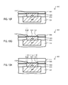
- FIG. 1 is a side cross sectional view of a storage element 100 according to a first embodiment.
- a storage element 100 can include a bottom structure 102 , an insulating layer 104 , a programmable layer 108 , and a top layer 110 .
- a bottom structure 102 can include an edge 112 formed at the intersection of a top surface 102 - 0 and a side surface 102 - 1 .
- An edge 112 can have, or present the possibility of, topography that can be adverse to very thin layers, like that described in FIG. 14 .
- FIG. 1 shows a bottom structure 102 having a side surface 102 - 1 that is perpendicular to a top surface 102 - 0
- other embodiments can have side surfaces that are sloped away from or toward a top surface (i.e., negative or positive slopes).
- a side surface 102 - 1 can also have a non-linear shape.
- a bottom structure 102 can be a bottom electrode, being formed of one or more conductive materials.
- a top electrode which may or may not include top layer 110 .
- a programmable layer 108 can include a solid electrolyte, and a bottom structure 102 can be an “inert” electrode, that does not include elements that ion conduct within programmable layer 108 .
- a bottom structure 102 serves as an inert electrode, it can be formed from any suitable conductive material or combination of conductive materials.
- a bottom electrode can include tantalum (Ta) and/or tungsten (W).
- a bottom structure 102 can include an active layer that is a source of one or more elements that can ion conduct within a programmable layer 108 .
- Such an active layer can include any of: a layer of one or more metals that ion conduct in programmable layer 108 ; an alloy of a metal that ion conducts in programmable layer 108 ; or a chalcogenide in combination with a metal that can ion conduct in programmable layer 108 .
- An insulating layer 104 can extend above a top surface 102 - 0 of bottom structure and can separate an edge 112 from programmable layer 108 to remove any adverse effects an edge 112 can present on overlying layers.
- An insulating layer 104 can be formed from any suitable insulating material or combination of insulating materials. In particular embodiments, an insulating layer 104 can be formed from silicon nitride.
- An opening 106 can be formed through insulating layer 104 to expose a top surface 102 - 0 of bottom structure 102 .
- An opening 106 can have a width (W) where it exposes the bottom structure 102 , and can be offset from edge 112 in a lateral direction. The offset amount is shown as “d” in FIG. 1 .
- An opening 106 can have sloped sides 114 to present a favorable topography for a subsequently deposited thin overlayer (e.g., programmable layer). While FIG. 1 shows an opening with sides having an essentially linear slope, alternate embodiments can include other slope types, including non-linear shapes.
- a programmable layer 108 can be formed within opening 106 , including along sloped sides 114 .
- a programmable layer 108 can be programmed between two or more impedance states in response to applied electric fields.
- An impedance state can be static or dynamic. That is, a programmable layer 108 can be programmed to an impedance state that remains substantially the same during a read (e.g., sense) operation. Alternatively, an impedance state can be dynamic, changing an impedance value during a read operation.
- an impedance can be a resistance, with the programmable layer 108 being programmed between two or more resistance values.
- a programmable layer 108 can be a solid electrolyte, and different impedance states can be established by an arrangement of one or more elements that ion conduct within the programmable layer 108 .
- a programmable layer 108 can include a metal oxide.
- a metal oxide can be a “high-K” dielectric material, having a dielectric constant greater than that of silicon dioxide.
- such a metal oxide can include any of: aluminum oxide, zirconium oxide, lanthanum oxide, hafnium oxide, or gadolinium oxide, including combinations of such layers.
- a programmable layer 108 can include a chalcogenide.
- a programmable layer 108 can be thin relative to other layers of a storage element 100 .
- the sloped sides 114 of opening 106 can enable a programmable layer 108 to be formed with substantially uniform thickness, in contrast to a structure like that of FIG. 14 , in which an edge can result in thinning.
- a programmable layer 108 can have a thickness (t) that is no more than 20% of an opening width (W).
- a programmable layer 108 can have a thickness of less than 50 nm, preferably less than 25 nm, even more preferably less than 10 nm.
- a top layer 110 can be formed over, and in contact with, programmable layer 108 .
- a top layer 110 can extend into opening 106 .
- a programmable layer 108 includes a solid electrolyte, and a top layer 110 can include an active layer that is in contact with programmable layer 108 .
- Such an active layer can be a source of one or more elements that can ion conduct within the programmable layer 108 .
- an active layer can include any of: a layer of one or more metals that ion conduct in programmable layer 108 ; an alloy of a metal that ion conducts in programmable layer 108 ; or a chalcogenide in combination with a metal that can ion conduct in programmable layer 108 .
- a top layer 110 can be an “inert” electrode that does not include elements that ion conduct within programmable layer 108 .
- a top layer 110 can be formed from any suitable conductive material or combination of conductive materials.
- FIG. 2 is a side cross sectional view of a storage element 200 according to another embodiment.
- a storage element 200 can include a bottom structure 202 , insulating layer 204 , opening 206 , and top layer 210 .
- Such structures can be subject to the same variations as described for FIG. 1 .
- Memory element 200 can differ from that of FIG. 1 in that a side surface 102 - 1 of bottom structure 102 can slope inward. Further, sloped sides 214 of opening 206 can form part of a same profile as side surface 202 - 1 .
- a storage element 200 can have a single side profile (e.g., linear as in FIG. 2 , or non-linear), with one portion of the profile including a side surface of bottom structure (e.g., 202 - 1 ) and another portion forming a sloped side of an opening (e.g., 214 ). Accordingly, unlike the storage element 100 of FIG. 1 , an opening 206 is not offset with respect to an edge 212 .
- FIG. 3 is a side cross sectional view of a storage element 300 according to a further embodiment.
- a storage element 300 can include a bottom structure 302 , insulating layer 304 , opening 306 , and top layer 310 .
- Such structures can be subject to the same variations as described for FIG. 1 .
- Storage element 300 can differ from that of FIG. 1 in that a programmable layer 308 can be formed below an insulating layer 304 .
- An opening 306 can be offset from an edge 312 of bottom structure 302 by a distance (shown as “d”), thus a top layer 310 does not contact programmable layer 308 in the vicinity of edge 312 . It is understood that in some embodiments an opening 306 can have sides 316 that are not sloped, but in other embodiments, sides 316 can be sloped.
- an embodiment like that of FIG. 2 can form storage elements that can follow a minimum opening size or feature size (i.e., a width “W” can be the size of a minimum opening achievable at manufactured layer, or minimum feature size at such a layer).
- a width “W” can be the size of a minimum opening achievable at manufactured layer, or minimum feature size at such a layer.
- FIGS. 1 and 3 which include an offset (“d”) between an edge of a bottom structure and the opening that exposes a bottom structure. That is, for an embodiment of FIG. 2 , a bottom structure 202 can have a width W, while in FIGS. 1 and 3 , a bottom structure 102 / 302 can have a width of W+2d (where W is the opening size).
- FIGS. 4A to 4I show a method of making of storage element 400 according to one particular embodiment.
- a storage element 400 can be one implementation of that shown in FIG. 1 .
- FIG. 4A shows an initial structure 400 ′ that includes a first lower interconnect (I/C) structure 418 formed in a first lower insulating layer 420 .
- First I/C structure 418 can be in contact with a second I/C structure 422 formed in a second lower insulating layer 424 .
- First and second I/C structure ( 418 / 422 ) can provide vertical interconnection to other conductive layers, a horizontal interconnection to other conductive layers, or combinations thereof.
- first I/C structure 418 can be a via (i.e., vertical interconnect structure) and second I/C structure 422 can be an interconnect pattern.
- a first I/C structure 418 can be a tungsten “plug”.
- a second I/C structure 422 can be a copper interconnect pattern.
- Lower insulating layers 420 / 424 can be formed from any suitable insulating material, including but not limited to silicon oxide (including doped and undoped forms); silicon nitride; silicon oxynitride; and/or polyimide, to name but a few.
- FIG. 4A shows a starting structure on which a storage element can be formed. That is, according to embodiments, a storage element can be formed on relatively higher layers of integrated circuit device (i.e., at the “backend” of a process). This is in sharp contrast to storage elements formed on a planar substrate.
- FIG. 4B shows the formation of a bottom structure insulating layer 415 over first I/C structure 418 and first lower insulating layer 420 .
- Insulating layer 415 can be formed of any suitable insulating material, including but not limited to: silicon oxide (including doped and undoped forms); silicon nitride; silicon oxynitride; and/or polyimide, to name but a few.
- FIG. 4C shows the formation of a bottom structure opening 426 through bottom structure insulating layer 415 that exposes lower I/C structure 418 .
- FIG. 4D shows the formation of bottom structure material(s) 402 ′.
- Such materials 402 ′ can be any of those described in embodiments herein, or equivalents, including those for an inert electrode, or alternatively, an active layer.
- bottom structure material 402 ′ can include tantalum.
- FIG. 4E shows an initial structure 400 ′ following planarization of a top surface.
- Such a step can remove portions of a bottom structure material 402 ′ to expose insulating layer 415 , and form bottom structure 402 .
- a bottom structure 402 can be formed with a “damascene” type process.
- Such a planarization can include cleaning steps.
- bottom structure 402 can include an edge 412 , which can present an adverse topography for subsequent thin layers, as noted in conjunction with FIG. 14 .
- FIG. 4F shows the formation of insulating layer 404 over bottom structure 402 , including over edges (e.g., 412 ).
- Insulating layer 404 can remove or reduce any unwanted irregularities of topography presented by an edge 412 .
- Insulating layer 404 can be formed of any suitable insulating material, including but not limited to silicon oxide (including doped and undoped forms); silicon oxynitride; silicon nitride and/or polyimide, to name but a few. In one very particular embodiment, insulating layer 404 can include silicon nitride.
- FIG. 4G shows the formation of opening 406 through insulating layer 404 to expose bottom structure 402 .
- Opening 406 can include sloped sides 414 .
- an opening 406 can be formed with an etching step having parameters appropriate for forming sloped sides 414 given the material(s) of insulating layer 404 .
- Opening 406 can be offset by a distance (d) from edge 412 .
- FIG. 4H shows the formation of programmable layer 408 over insulating layer 404 and within opening 406 , including on sloped sides 414 .
- a programmable layer 408 can be formed from any of those materials noted for embodiments herein, or equivalents. As noted above, a programmable layer 408 can be relatively thin as compared other layers of a storage element. A programmable layer 408 can have any of the thicknesses described for programmable layer 108 in FIG. 1 above.
- FIG. 4I shows the formation of a top layer 410 over programmable layer 408 and within opening 406 .
- a top layer 410 can be formed from any of those materials noted for embodiments herein, or equivalents.
- a programmable layer 408 can include a solid electrolyte and a top layer 410 can be an active layer, providing one or elements that ion conduct in the solid electrolyte.
- a programmable layer 408 can include a solid electrolyte and a top layer 410 can be an inert electrode.
- a top layer 410 can be common to multiple storage elements, forming a “plate” structure.
- top layer 410 can be formed over top layer 410 .
- FIGS. 5A to 5G show a method of making of storage element 500 according to another particular embodiment.
- the embodiment of FIGS. 5A to 5G can differ from that of FIGS. 4A to 4I in that a bottom structure can be formed with a patterning step, as opposed to a damascene approach.
- a storage element 500 can be another implementation of that shown in FIG. 1 .
- FIG. 5A shows an initial structure 500 ′ like that of FIG. 4A , and can be subject to the variations noted for FIG. 4A .
- FIG. 5B shows the formation of a bottom structure material(s) layer 502 ′.
- Such materials can include any of those noted in FIG. 4D , or equivalents.
- FIG. 5C shows a patterning step that can pattern bottom structure materials to create a bottom structure 502 .
- such an action can include lithography and etch steps.
- a bottom structure 502 can be formed by patterning.
- the formation of bottom structure 502 can include an edge 512 , which can present an adverse topography for subsequent thin layers, in conventional approaches like that of FIG. 14 .
- FIG. 5D shows the formation of insulating layer 504 over bottom structure 502 , including over edges (e.g., 512 ).
- Insulating layer 404 can be formed of any suitable insulating material, including those noted in FIG. 4F .
- insulating layer 504 can be silicon nitride.
- FIG. 5E shows the formation of opening 506 through insulating layer 504 to expose bottom structure 502 .
- Opening 506 can include sloped sides 514 .
- an opening 506 can be formed with an etching step having parameters appropriate for forming sloped sides 514 given the material(s) of insulating layer 504 .
- opening 506 can be offset by a distance (d) from edge 512 .
- FIG. 5F shows the formation of programmable layer 508 over insulating layer 504 and within opening 506 , including on sloped sides 514 .
- a programmable layer 508 can be formed from any of those materials noted for embodiments herein, or equivalents, and can be a relatively thin layer, as compared other layers of a storage element.
- a programmable layer 508 can have any of the thicknesses described for layer 108 in FIG. 1 above.
- FIG. 5G shows the formation of a top layer 510 over programmable layer 508 and within opening 506 .
- a top layer 510 can be formed from any of those materials noted for embodiments herein, or equivalents. It is also understood that a top layer 510 can be a plate layer and/or additional layers can be formed over top layer 510 .
- FIGS. 6A to 6H show a method of making of storage element 600 according to another particular embodiment.
- the embodiment of FIGS. 6A to 6H can differ from that of FIGS. 4A to 4I in that a bottom structure can be formed at a lower level in an integrated circuit layer hierarchy.
- a storage element 600 can be another implementation of that shown in FIG. 1 .
- FIG. 6A shows an initial structure 600 ′ that includes a lower I/C structure 622 formed in a lower insulating layer 624 .
- I/C structure 622 can provide vertical interconnection to other conductive layers, a horizontal interconnection to other conductive layers, or combinations thereof.
- an I/C structure 622 can be a copper interconnect pattern.
- Lower insulating layer 624 can be formed from any suitable insulating material, including but not limited to silicon oxide (including doped and undoped forms); silicon nitride; silicon oxynitride; and/or polyimide, to name but a few.
- a bottom structure insulating layer 615 can be formed over I/C structure 622 and insulating layer 624 .
- Insulating layer 615 can be formed of any suitable insulating material, and in particular embodiments, can be silicon nitride.
- FIG. 6B shows the formation of a bottom structure opening 626 through bottom structure insulating layer 615 that exposes lower I/C structure 622 .
- an opening formation step can utilize an existing via patterning approach.
- a same etch mask used to create an opening for I/C structure 418 can be used to create opening 626 . More particularly, if a fabrication process has a via formation mask, such a mask can be utilized in the formation of bottom structures of a storage element 600 .
- FIG. 6C shows the formation of bottom structure material(s) 602 ′.
- Such materials 602 ′ can be any of those described in embodiments herein, or equivalents, including those for an inert electrode, or alternatively, an active layer.
- bottom structure material 602 ′ can be tantalum.
- FIG. 6D shows an initial structure 600 ′ following a planarization of a top surface for a damascene type formation of a bottom structure 602 having an edge 612 .
- FIGS. 6E to 6H can follow the same general formation steps as FIGS. 4F to 4I , respectively.
- the storage element 600 can exist at a different (e.g., lower) fabrication level than that of FIG. 4I .
- An insulating layer 604 can be formed over bottom structure ( FIG. 6E ).
- An opening 606 with sloped sides 614 can be formed through insulating layer 604 that is offset from edge 612 ( FIG. 6F ).
- a programmable layer 608 can be formed in the opening 606 on the sloped sides 614 ( FIG. 6G ).
- a top layer 610 can be formed on programmable layer 608 including within opening 606 .
- FIGS. 7A to 7J show a method of making of storage element 700 according to another particular embodiment.
- the embodiment of FIGS. 7A to 7J can differ from that of FIGS. 4A to 4I in that a programmable layer is not formed within an opening, but rather below an opening.
- the embodiment of FIGS. 7A to 7J can utilize an etch stop layer to control the formation of an opening to a programmable layer.
- a storage element 700 can be one implementation of that shown in FIG. 3 .
- FIGS. 7A to 7D can follow the same or equivalent actions as FIGS. 6A to 6D .
- FIG. 7E shows the formation of programmable layer 708 over bottom structure 702 , including over edge 712 .
- a programmable layer 708 can be formed from any of those materials noted for embodiments herein, or equivalents, and can be a relatively thin layer, as compared other layers of a storage element. As understood from FIG. 14 , formation of programmable layer 708 over edge 712 can result in an adverse narrowing of programmable layer 708 .
- a programmable layer 708 can have a thickness as described for layer 108 of FIG. 1 , including a thickness relative to a width (W) of an opening (the opening is formed subsequently in FIGS. 7I and 7J ).
- FIG. 7F shows the formation of an etch stop layer 728 over programmable layer 708 .
- a etch stop layer 728 can protect a programmable layer 708 from being etched during the formation of an opening.
- the material(s) of an etch stop layer 728 can be selected based on a subsequently formed insulating layer ( 704 ) and an etch process used to form an opening.
- FIG. 7G shows the formation of insulating layer 704 over etch stop layer 728 , including over locations of an edge 712 .
- Insulating layer 704 can be formed of any suitable insulating material as noted for embodiments herein, or equivalents.
- FIG. 7H shows the formation of a partial opening 706 ′ through insulating layer 704 down to etch stop layer 728 .
- formation of partial opening 706 ′ can include an etch that is highly selective between etch stop layer 728 and insulating layer 704 .
- etch stop 728 can prevent programmable layer 708 from being etched when an opening is created in insulating layer 704 .
- partial opening 706 ′ can be offset with respect to edge 712 by a distance “d”.
- FIG. 7I shows the completion of opening 706 through insulating layer 704 and etch stop layer 728 to expose programmable layer 708 .
- Such a step can include employing an etch that is highly selective between etch stop layer 728 and programmable layer 708 .
- Opening 706 can include sides 718 with profiles that are sloped or that are substantially vertical. As shown, opening 706 can be offset with respect to edge 712 .
- FIG. 7J shows the formation of a top layer 710 into opening 706 and in contact with programmable layer 708 . Due to offset distance “d”, top layer 710 does not contact programmable layer 708 at a location that can suffer from thinning (e.g., at edge 712 ).
- a top layer 710 can be formed from any of those materials noted for embodiments herein, or equivalents. It is also understood that a top layer 710 can be a plate layer and/or additional layers can be formed over top layer 710 .
- FIGS. 8A to 8H show a method of making of storage element 800 according to a further particular embodiment.
- the embodiment of FIGS. 8A to 8H can include approaches like those of FIGS. 7A to 7J , but with a bottom structure being formed by patterning, and not a damascene type approach.
- a storage element 800 can be one implementation of that shown in FIG. 3 .
- FIG. 8A shows the formation of a bottom structure material(s) layer 802 ′.
- Bottom structure material(s) 802 ′ can be formed on, and in contact with, an I/C structure 822 .
- An I/C structure 822 can provide vertical interconnection to other conductive layers, horizontal interconnection to other conductive layers, or combinations thereof.
- an I/C structure 822 can be a copper interconnect pattern.
- I/C structure 822 can be formed in lower insulating layer 824 which can be formed from any suitable insulating material, as described for embodiments herein.
- FIG. 8B shows a patterning step that can pattern bottom structure materials to create a bottom structure 802 .
- Such an action can include steps like those of FIG. 5C , or equivalents.
- a bottom structure 802 can be an inert electrode, or alternatively an active layer, as described for embodiments herein.
- a bottom structure 802 can include an edge 812 .
- FIG. 8C shows the formation of insulating layer 815 over bottom structure 802 , and a subsequent planarization step.
- a top surface of bottom structure 802 can be exposed.
- Such a step can result in topography at edge 812 that can be adverse to very thin layers.
- FIG. 8D shows the formation of a programmable layer 808 over bottom structure 802 , including over edge 812 .
- a programmable layer 808 can be formed from any of those materials noted for embodiments herein, or equivalents, and can be a relatively thin layer, as compared other layers of a storage element. As understood from FIG. 14 , formation of programmable layer 808 over edge 812 can result in an adverse narrowing of programmable layer 808 .
- FIG. 8D also shows the formation of an etch stop layer 828 over programmable layer 808 .
- a etch stop layer 828 can protect a programmable layer 808 and be selected in the same or an equivalent manner, to etch layer 728 described for FIGS. 7E to 7I .
- FIGS. 8E to 8H can follow actions like those described for FIGS. 7G to 7J , or equivalents. This can include: the formation of insulating layer 804 ( FIG. 8E ); etching through insulating layer 804 to etch stop layer 828 ( FIG. 8F ); removing etch stop layer 828 to create opening 806 and expose programmable layer 808 ( FIG. 8G ); and forming top layer 810 in opening 806 in contact with programmable layer 808 .
- FIGS. 9A to 9F show a method of making of storage element 900 according to a further particular embodiment.
- the embodiment of FIGS. 9A to 9F can include approaches like those of FIGS. 6A to 6H , forming a bottom structure at a lower level in an integrated circuit layer hierarchy.
- a bottom structure can be formed by patterning, as opposed to a damascene type approach.
- a storage element 900 can be one implementation of that shown in FIG. 1 .
- FIGS. 9A to 9C can include actions like those shown in FIGS. 5B to 5D , or equivalents, but performed on a lower level in an interconnect hierarchy. Such actions can result in an initial storage element structure 900 ′ having a bottom structure 902 with an edge 912 covered with an insulating layer 904 .
- FIGS. 9D to 9F can include actions like those shown in FIGS. 4G to 4I , or equivalents, but performed on a lower level of an interconnect hierarchy. Such actions can result in a programmable layer 908 formed on sloped sides 914 of an opening 906 that is offset (by a distance d) from the edge 912 of a bottom structure 902 .
- FIGS. 7A to 7J includes an etch stop layer 728 to protect a programmable layer 708 during the formation of an opening
- a programmable layer can be sufficiently robust, or an etch sufficiently selective between a programmable layer and overlying insulating layer(s) that an etch stop layer can be excluded.
- Such embodiments are shown in FIGS. 10A to 10H and 11A to 11G .
- FIGS. 10A to 10H show a method of making of storage element 1000 according to a further particular embodiment.
- the embodiment of FIGS. 10A to 10H can include approaches like those of FIGS. 7A to 7J , however, without the inclusion of an etch stop layer.
- a storage element 1000 can be one implementation of that shown in FIG. 3 .
- FIGS. 10A to 10E can include actions like those of FIGS. 7A to 7E , or equivalents.
- FIG. 10F shows the formation of insulating layer 1004 on programmable layer 1008 , as opposed to an etch stop layer.
- FIG. 10G shows the formation of an opening 1006 through insulating layer 1004 that is offset from an edge 1012 by a distance “d”.
- FIG. 10H shows the formation of a top layer 1010 over programmable layer 1008 .
- steps can include variations of other embodiments herein.
- FIGS. 11A to 11G show a method of making of storage element 1100 according to a further particular embodiment.
- the embodiment of FIGS. 11A to 11G can include approaches like those of FIGS. 8A to 8H , however, without the inclusion of an etch stop layer.
- a storage element 1100 can be one implementation of that shown in FIG. 3 .
- FIGS. 11A to 11C can include actions like those of FIGS. 8A to 8C , or equivalents.
- FIG. 11E shows the formation of insulating layer 1104 on programmable layer 1108 , as opposed to an etch stop layer. Further, FIG. 11F shows the formation of an opening 1006 through insulating layer 1004 that is offset from an edge 1012 by a distance “d”. FIG. 11G shows the formation of a top layer 1110 over programmable layer 1108 . Such steps can include variations of other embodiments herein.
- FIGS. 12A to 12E show a method of making of storage element 1200 according to another particular embodiment.
- a storage element 1200 can be one implementation of that shown in FIG. 2 .
- FIG. 12A shows an initial structure 1200 ′ that includes an initial bottom structure 1202 ′, a first lower I/C structure 1218 formed in a first lower insulating layer 1220 in contact with a second I/C structure 1222 formed in a second lower insulating layer 1224 .
- First and second I/C structure ( 1218 / 1222 ) can provide vertical interconnection to other conductive layers as described for embodiments herein.
- Lower insulating layers 1220 / 1224 can be formed from any suitable insulating material, as described for embodiments herein, or equivalents.
- An initial bottom structure 1202 ′ can be formed in an insulating layer 1204 , and can have an initial top surface 1202 - 0 ′ and a sloped side surface 1202 - 1 .
- an initial bottom structure 1202 ′ can be formed with damascene techniques that create an opening with sloped sides.
- etching techniques e.g., “over etching”
- a patterning step e.g., lithography and etch
- An initial bottom structure 1202 ′ can be formed from any of the bottom structure materials described for embodiments herein, or equivalents, including those for an inert electrode, or alternatively, an active layer. However, such a material is capable of being transformed (e.g., oxidized) into another material for subsequent removal. In one very particular embodiment, an initial bottom structure 1202 ′ can be tantalum.
- FIG. 12B shows the transformation of a top portion of initial bottom structure 1202 ′ to create removable portion 1230 .
- a removable portion 1230 can be created by oxidizing a surface of initial bottom structure 1202 ′. It is understood that removable portion 1230 can be removed to leave a remaining portion of the initial bottom structure 1202 ′.
- FIG. 12C shows the structure 1200 ′ after removing the removable portion 1230 .
- such an action can include etching with an etch that is highly selective between the bottom structure 1202 and removable portion 1203 .
- an initial structure 1200 ′ can include an opening 1206 that exposes a top surface 1202 - 0 of bottom structure 1202 .
- Such an opening 1206 can include a sloped side 1214 . Sloped side 1214 can follow the profile of the side surface 1202 - 1 of bottom structure 1202 .
- the bottom structure 1202 can include an edge 1212 .
- FIG. 12D shows the formation of programmable layer 1208 within opening 1206 along sloped sides 1214 .
- a programmable layer 1208 can be formed from any of those materials noted for embodiments herein, or equivalents. As noted above, a programmable layer 1208 can be relatively thin compared other layers of a storage element. A programmable layer 1208 can have any of the thicknesses described for FIG. 1 above. Due the sloped sides 1214 of opening, a programmable layer 1208 can avoid the narrowing that can occur in conventional approaches, like that of FIG. 14 .
- FIG. 12E shows the formation of a top layer 1210 over programmable layer 1208 and within opening 1206 .
- a top layer 1210 can be formed from any of those materials noted for embodiments herein, or equivalents. It is also understood that a top layer 1210 can be a plate layer and/or additional layers can be formed over top layer 1210 .
- FIGS. 13A to 13D show a method of making of storage element 1300 according to another particular embodiment.
- a storage element 1300 can be one implementation of that shown in FIG. 2 .
- FIG. 13A shows an initial structure 1300 ′ like that of FIG. 12A .
- Such an initial structure 1300 ′ can include materials and can be formed in same or an equivalent fashion.
- FIG. 13B shows the initial structure 1300 ′ after removing a top portion of an initial bottom structure 1302 ′.
- such an action can include etching with an etch that is highly selective between insulating layer 1304 and a bottom structure 1302 .
- a removal step can include any techniques suitable for the materials uses, including but not limited to: dry etching, wet etching, and/or chemical-mechanical polishing (CMP).
- CMP chemical-mechanical polishing
- an initial structure 1300 ′ can include an opening 1306 that exposes a top surface 1302 - 0 of bottom structure 1302 .
- Such an opening 1306 can include a sloped side 1314 that can follow the profile of the side surface 1302 - 1 of bottom structure 1302 .
- Bottom structure 1302 can include an edge 1312 .
- FIGS. 13C and 13D show processes like those of FIGS. 12D and 12E , and can include the same or equivalent materials and process steps.
Landscapes
- Engineering & Computer Science (AREA)
- Manufacturing & Machinery (AREA)
- Semiconductor Memories (AREA)
Abstract
Description
Claims (9)
Priority Applications (2)
| Application Number | Priority Date | Filing Date | Title |
|---|---|---|---|
| US13/830,315 US9412945B1 (en) | 2013-03-14 | 2013-03-14 | Storage elements, structures and methods having edgeless features for programmable layer(s) |
| US15/214,224 US9595671B1 (en) | 2013-03-14 | 2016-07-19 | Methods of fabricating storage elements and structures having edgeless features for programmable layer(s) |
Applications Claiming Priority (1)
| Application Number | Priority Date | Filing Date | Title |
|---|---|---|---|
| US13/830,315 US9412945B1 (en) | 2013-03-14 | 2013-03-14 | Storage elements, structures and methods having edgeless features for programmable layer(s) |
Related Child Applications (1)
| Application Number | Title | Priority Date | Filing Date |
|---|---|---|---|
| US15/214,224 Division US9595671B1 (en) | 2013-03-14 | 2016-07-19 | Methods of fabricating storage elements and structures having edgeless features for programmable layer(s) |
Publications (1)
| Publication Number | Publication Date |
|---|---|
| US9412945B1 true US9412945B1 (en) | 2016-08-09 |
Family
ID=56556019
Family Applications (2)
| Application Number | Title | Priority Date | Filing Date |
|---|---|---|---|
| US13/830,315 Active 2034-10-20 US9412945B1 (en) | 2013-03-14 | 2013-03-14 | Storage elements, structures and methods having edgeless features for programmable layer(s) |
| US15/214,224 Active US9595671B1 (en) | 2013-03-14 | 2016-07-19 | Methods of fabricating storage elements and structures having edgeless features for programmable layer(s) |
Family Applications After (1)
| Application Number | Title | Priority Date | Filing Date |
|---|---|---|---|
| US15/214,224 Active US9595671B1 (en) | 2013-03-14 | 2016-07-19 | Methods of fabricating storage elements and structures having edgeless features for programmable layer(s) |
Country Status (1)
| Country | Link |
|---|---|
| US (2) | US9412945B1 (en) |
Citations (17)
| Publication number | Priority date | Publication date | Assignee | Title |
|---|---|---|---|---|
| US5761115A (en) | 1996-05-30 | 1998-06-02 | Axon Technologies Corporation | Programmable metallization cell structure and method of making same |
| US6825489B2 (en) | 2001-04-06 | 2004-11-30 | Axon Technologies Corporation | Microelectronic device, structure, and system, including a memory structure having a variable programmable property and method of forming the same |
| US20050226062A1 (en) | 2003-03-20 | 2005-10-13 | Sony Corporation | Memory element and storage device using this |
| US7126152B2 (en) | 2003-12-03 | 2006-10-24 | Sony Corporation | Storage device |
| US20090173930A1 (en) * | 2008-01-09 | 2009-07-09 | Sony Corporation | Memory element and memory device |
| US7675053B2 (en) | 2005-01-11 | 2010-03-09 | Sony Corporation | Memory device comprising a memory layer and a metal chalcogenide ion-source layer |
| US7719082B2 (en) | 2003-11-28 | 2010-05-18 | Sony Corporation | Memory device and storage apparatus |
| US7772029B2 (en) | 2004-11-15 | 2010-08-10 | Sony Corporation | Memory element and memory device comprising memory layer positioned between first and second electrodes |
| US20100264394A1 (en) | 2009-04-16 | 2010-10-21 | Sony Corporation | Semiconductor memory and method of manufacturing the same |
| US20110027597A1 (en) | 2009-07-28 | 2011-02-03 | Sony Corporation | Target, method for producing the same, memory, and method for producing the same |
| US20110031466A1 (en) | 2009-08-05 | 2011-02-10 | Sony Corporation | Semiconductor memory device and a method of manufacturing the same |
| US20110194329A1 (en) | 2010-02-09 | 2011-08-11 | Sony Corporation | Memory component, memory device, and method of operating memory device |
| US8115586B2 (en) | 2006-04-28 | 2012-02-14 | Sharp Kabushiki Kaisha | Variable resistance element, and its manufacturing method |
| US8222713B2 (en) | 2005-12-02 | 2012-07-17 | Sony Corporation | Storage element and storage apparatus |
| US8242552B2 (en) | 2009-04-02 | 2012-08-14 | Sony Corporation | Storage element, method of manufacturing same, and semiconductor storage device |
| US8295074B2 (en) | 2007-11-29 | 2012-10-23 | Sony Corporation | Memory cell |
| US8426839B1 (en) | 2009-04-24 | 2013-04-23 | Adesto Technologies Corporation | Conducting bridge random access memory (CBRAM) device structures |
-
2013
- 2013-03-14 US US13/830,315 patent/US9412945B1/en active Active
-
2016
- 2016-07-19 US US15/214,224 patent/US9595671B1/en active Active
Patent Citations (20)
| Publication number | Priority date | Publication date | Assignee | Title |
|---|---|---|---|---|
| US5761115A (en) | 1996-05-30 | 1998-06-02 | Axon Technologies Corporation | Programmable metallization cell structure and method of making same |
| US6825489B2 (en) | 2001-04-06 | 2004-11-30 | Axon Technologies Corporation | Microelectronic device, structure, and system, including a memory structure having a variable programmable property and method of forming the same |
| US20050226062A1 (en) | 2003-03-20 | 2005-10-13 | Sony Corporation | Memory element and storage device using this |
| US20110073825A1 (en) | 2003-11-28 | 2011-03-31 | Sony Corporation | Memory device and storage apparatus |
| US7719082B2 (en) | 2003-11-28 | 2010-05-18 | Sony Corporation | Memory device and storage apparatus |
| US20100135060A1 (en) | 2003-11-28 | 2010-06-03 | Sony Corporation | Memory device and storage apparatus |
| US7126152B2 (en) | 2003-12-03 | 2006-10-24 | Sony Corporation | Storage device |
| US7772029B2 (en) | 2004-11-15 | 2010-08-10 | Sony Corporation | Memory element and memory device comprising memory layer positioned between first and second electrodes |
| US7786459B2 (en) | 2004-11-15 | 2010-08-31 | Sony Corporation | Memory element and memory device comprising memory layer positioned between first and second electrodes |
| US7675053B2 (en) | 2005-01-11 | 2010-03-09 | Sony Corporation | Memory device comprising a memory layer and a metal chalcogenide ion-source layer |
| US8222713B2 (en) | 2005-12-02 | 2012-07-17 | Sony Corporation | Storage element and storage apparatus |
| US8115586B2 (en) | 2006-04-28 | 2012-02-14 | Sharp Kabushiki Kaisha | Variable resistance element, and its manufacturing method |
| US8295074B2 (en) | 2007-11-29 | 2012-10-23 | Sony Corporation | Memory cell |
| US20090173930A1 (en) * | 2008-01-09 | 2009-07-09 | Sony Corporation | Memory element and memory device |
| US8242552B2 (en) | 2009-04-02 | 2012-08-14 | Sony Corporation | Storage element, method of manufacturing same, and semiconductor storage device |
| US20100264394A1 (en) | 2009-04-16 | 2010-10-21 | Sony Corporation | Semiconductor memory and method of manufacturing the same |
| US8426839B1 (en) | 2009-04-24 | 2013-04-23 | Adesto Technologies Corporation | Conducting bridge random access memory (CBRAM) device structures |
| US20110027597A1 (en) | 2009-07-28 | 2011-02-03 | Sony Corporation | Target, method for producing the same, memory, and method for producing the same |
| US20110031466A1 (en) | 2009-08-05 | 2011-02-10 | Sony Corporation | Semiconductor memory device and a method of manufacturing the same |
| US20110194329A1 (en) | 2010-02-09 | 2011-08-11 | Sony Corporation | Memory component, memory device, and method of operating memory device |
Also Published As
| Publication number | Publication date |
|---|---|
| US9595671B1 (en) | 2017-03-14 |
Similar Documents
| Publication | Publication Date | Title |
|---|---|---|
| US11094744B2 (en) | Interconnect landing method for RRAM technology | |
| US9553265B1 (en) | RRAM device with data storage layer having increased height | |
| US11075335B2 (en) | Techniques for MRAM MTJ top electrode connection | |
| KR101974300B1 (en) | Memory structures and associated cross-point memory arrays, electronic systems, and methods of forming memory structures | |
| US9577186B2 (en) | Non-volatile resistive oxide memory cells and methods of forming non-volatile resistive oxide memory cells | |
| KR101671632B1 (en) | An improved resistive random access memory (rram) structure | |
| CN106252505B (en) | RRAM device and method | |
| US8816314B2 (en) | Contact structure and method for variable impedance memory element | |
| KR101626225B1 (en) | Protective sidewall techniques for rram | |
| US20160260899A1 (en) | Methods of Forming a Non-Volatile Resistive Oxide Memory Cell and Methods of Forming a Non-Volatile Resistive Oxide Memory Array | |
| GB2584021A (en) | Logic chip including embedded magnetic tunnel junctions | |
| US11785786B2 (en) | Trench formation scheme for programmable metallization cell to prevent metal redeposit | |
| EP3940779A1 (en) | Method of forming three-dimensional memory device | |
| US8895953B1 (en) | Programmable memory elements, devices and methods having physically localized structure | |
| JP2006060207A (en) | Etching solution and method of forming magnetic memory device utilizing it | |
| US9208868B2 (en) | Semiconductor device including a variable resistance device, and method of controlling the semiconductor device | |
| US9595671B1 (en) | Methods of fabricating storage elements and structures having edgeless features for programmable layer(s) | |
| CN114121817B (en) | Memory device and method of forming the same | |
| US20210225936A1 (en) | Memory devices and methods of forming memory devices | |
| TWI740787B (en) | Semiconductor structure and method of forming the same | |
| CN115915755A (en) | Preparation method of semiconductor structure and semiconductor structure | |
| CN118280822A (en) | Method for manufacturing semiconductor device | |
| KR20110125053A (en) | Method for manufacturing semiconductor device | |
| KR20140145529A (en) | Contact structure and method for variable impedance memory element |
Legal Events
| Date | Code | Title | Description |
|---|---|---|---|
| AS | Assignment |
Owner name: OPUS BANK, CALIFORNIA Free format text: SECURITY INTEREST;ASSIGNORS:ADESTO TECHNOLOGIES CORPORATION;ARTEMIS ACQUISITION LLC;REEL/FRAME:035754/0580 Effective date: 20150430 |
|
| AS | Assignment |
Owner name: ADESTO TECHNOLOGIES CORPORATION, CALIFORNIA Free format text: ASSIGNMENT OF ASSIGNORS INTEREST;ASSIGNORS:TSAI, KUEI CHANG;SHIELDS, JEFFREY ALLAN;VERRIER, PASCAL;SIGNING DATES FROM 20150518 TO 20160519;REEL/FRAME:039192/0328 Owner name: ALTIS SEMICONDUCTOR S.N.C., FRANCE Free format text: ASSIGNMENT OF ASSIGNORS INTEREST;ASSIGNORS:TSAI, KUEI CHANG;SHIELDS, JEFFREY ALLAN;VERRIER, PASCAL;SIGNING DATES FROM 20150518 TO 20160519;REEL/FRAME:039192/0328 |
|
| STCF | Information on status: patent grant |
Free format text: PATENTED CASE |
|
| AS | Assignment |
Owner name: ARTEMIS ACQUISITION LLC, CALIFORNIA Free format text: RELEASE BY SECURED PARTY;ASSIGNOR:WESTERN ALLIANCE BANK;REEL/FRAME:044219/0610 Effective date: 20171003 Owner name: ADESTO TECHNOLOGIES CORPORATION, CALIFORNIA Free format text: RELEASE BY SECURED PARTY;ASSIGNOR:WESTERN ALLIANCE BANK;REEL/FRAME:044219/0610 Effective date: 20171003 |
|
| AS | Assignment |
Owner name: OBSIDIAN AGENCY SERVICES, INC., AS COLLATERAL AGENT, CALIFORNIA Free format text: SECURITY INTEREST;ASSIGNORS:ADESTO TECHNOLOGIES CORPORATION;ARTEMIS ACQUISITION LLC;REEL/FRAME:046105/0731 Effective date: 20180508 Owner name: OBSIDIAN AGENCY SERVICES, INC., AS COLLATERAL AGEN Free format text: SECURITY INTEREST;ASSIGNORS:ADESTO TECHNOLOGIES CORPORATION;ARTEMIS ACQUISITION LLC;REEL/FRAME:046105/0731 Effective date: 20180508 |
|
| AS | Assignment |
Owner name: ADESTO TECHNOLOGIES CORPORATION, CALIFORNIA Free format text: RELEASE BY SECURED PARTY;ASSIGNOR:OPUS BANK;REEL/FRAME:049125/0970 Effective date: 20160707 Owner name: ARTEMIS ACQUISITION LLC, CALIFORNIA Free format text: RELEASE BY SECURED PARTY;ASSIGNOR:OPUS BANK;REEL/FRAME:049125/0970 Effective date: 20160707 |
|
| AS | Assignment |
Owner name: ARTEMIS ACQUISITION LLC, CALIFORNIA Free format text: RELEASE BY SECURED PARTY;ASSIGNOR:OBSIDIAN AGENCY SERVICES, INC., AS COLLATERAL AGENT;REEL/FRAME:050480/0836 Effective date: 20190923 Owner name: ADESTO TECHNOLOGIES CORPORATION, CALIFORNIA Free format text: RELEASE BY SECURED PARTY;ASSIGNOR:OBSIDIAN AGENCY SERVICES, INC., AS COLLATERAL AGENT;REEL/FRAME:050480/0836 Effective date: 20190923 |
|
| MAFP | Maintenance fee payment |
Free format text: PAYMENT OF MAINTENANCE FEE, 4TH YEAR, LARGE ENTITY (ORIGINAL EVENT CODE: M1551); ENTITY STATUS OF PATENT OWNER: LARGE ENTITY Year of fee payment: 4 |
|
| AS | Assignment |
Owner name: GLOBALFOUNDRIES U.S. INC., NEW YORK Free format text: ASSIGNMENT OF ASSIGNORS INTEREST;ASSIGNOR:RENESAS DESIGN US INC. (FORMERLY KNOWN AS DIALOG SEMICONDUCTOR US INC. AS SUCCESSOR-IN-INTEREST TO ADESTO TECHNOLOGIES CORPORATION AND ARTEMIS ACQUISITION, LLC);REEL/FRAME:063118/0352 Effective date: 20230203 |
|
| MAFP | Maintenance fee payment |
Free format text: PAYMENT OF MAINTENANCE FEE, 8TH YEAR, LARGE ENTITY (ORIGINAL EVENT CODE: M1552); ENTITY STATUS OF PATENT OWNER: LARGE ENTITY Year of fee payment: 8 |