US9412640B2 - Semiconductor device including substrate contact and related method - Google Patents
Semiconductor device including substrate contact and related method Download PDFInfo
- Publication number
- US9412640B2 US9412640B2 US13/749,830 US201313749830A US9412640B2 US 9412640 B2 US9412640 B2 US 9412640B2 US 201313749830 A US201313749830 A US 201313749830A US 9412640 B2 US9412640 B2 US 9412640B2
- Authority
- US
- United States
- Prior art keywords
- contact
- substrate
- semiconductor device
- node
- polysilicon
- Prior art date
- Legal status (The legal status is an assumption and is not a legal conclusion. Google has not performed a legal analysis and makes no representation as to the accuracy of the status listed.)
- Expired - Fee Related, expires
Links
Images


Classifications
-
- H—ELECTRICITY
- H01—ELECTRIC ELEMENTS
- H01L—SEMICONDUCTOR DEVICES NOT COVERED BY CLASS H10
- H01L21/00—Processes or apparatus adapted for the manufacture or treatment of semiconductor or solid state devices or of parts thereof
- H01L21/70—Manufacture or treatment of devices consisting of a plurality of solid state components formed in or on a common substrate or of parts thereof; Manufacture of integrated circuit devices or of parts thereof
- H01L21/71—Manufacture of specific parts of devices defined in group H01L21/70
- H01L21/74—Making of localized buried regions, e.g. buried collector layers, internal connections substrate contacts
- H01L21/743—Making of internal connections, substrate contacts
-
- H10W20/021—
-
- H01L29/945—
-
- H—ELECTRICITY
- H10—SEMICONDUCTOR DEVICES; ELECTRIC SOLID-STATE DEVICES NOT OTHERWISE PROVIDED FOR
- H10D—INORGANIC ELECTRIC SEMICONDUCTOR DEVICES
- H10D1/00—Resistors, capacitors or inductors
- H10D1/60—Capacitors
- H10D1/62—Capacitors having potential barriers
- H10D1/66—Conductor-insulator-semiconductor capacitors, e.g. MOS capacitors
- H10D1/665—Trench conductor-insulator-semiconductor capacitors, e.g. trench MOS capacitors
Definitions
- Embodiments of this disclosure relate generally to semiconductor devices and, more particularly, to a semiconductor device including a substrate contact formed from portions of a deep trench (e.g., a trench capacitor), a related method and design structure.
- a deep trench e.g., a trench capacitor
- contacts e.g., substrate contacts, low resistance contacts, contacts to an N+ buried plate, etc.
- Formation of these contacts frequently requires inclusion of a number of steps in the semiconductor manufacturing/fabrication process. These steps include etching portions of the semiconductor device to go through formed layers and expose the substrate and/or using a device contact level silicide and/or a (MOL) metal to connect to the N+ buried plate. These processes require a hole to be formed/etched through layers of the semiconductor device and the contact to be positioned within the hole formed in the existing structure.
- etching these holes/contacts and creating a low resistance contact may be problematic due to process integration adjustments and requirements. Further, this etching and formation may create structures on the wafers which are problematic for an integrated process flow (e.g., a non-planar contact structure, deep hole on the wafer, etc.).
- a first aspect of the disclosure provides a method including: forming a mask on the semiconductor device, the mask exposing at least one contact region including a trench disposed in a substrate of the semiconductor device; performing a first substrate contact etch on the semiconductor device, the first substrate contact etch recessing the exposed contact region within the trench; removing a set of node films disposed above the exposed contact region and on the sides of the trench; and forming a contact within the trench to the substrate.
- a second aspect of the disclosure provides a method of forming a contact on a semiconductor device, the method comprising: forming a mask on the semiconductor device, the semiconductor device including a set of contact nodes and the mask exposing at least one contact node disposed within a trench in a substrate of the semiconductor device; performing a first substrate contact etch on the semiconductor device, the first substrate contact etch recessing the at least one exposed contact node within the trench; removing the mask from the semiconductor device; performing a second substrate contact etch on the semiconductor device, the second substrate contact etch recessing the set of contact nodes within the semiconductor device; removing a set of node films disposed above the set of contact nodes and on the sides of the trench; and forming a contact region within the trench above the contact nodes.
- a third aspect of the disclosure provides a method of forming a semiconductor device, the method including: method of forming a contact on a semiconductor device, the method comprising: masking regions of the semiconductor device other than a set of substrate contacts, the set of substrate contacts including a set of contact nodes disposed within a trench in a substrate of the semiconductor device; etching about the set of substrate contacts on the semiconductor device; removing a portion of the set of contact nodes from the trench; and forming a contact region within the trench above the set of contact nodes, the contact region substantially connected to the set of contact nodes and the substrate.
- FIG. 1 is a demonstrative illustration of a portion of a semiconductor device according to an embodiment of the invention.
- FIGS. 2-7 are demonstrative illustrations of a method of forming a semiconductor device according to embodiments of the invention.
- FIG. 8 shows a demonstrative illustration of a method flow diagram illustrating steps in a method of forming an integrated circuit (IC) in accordance with an embodiment.
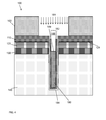
- FIG. 1 is a demonstrative illustration of a cross sectional view of a portion of a semiconductor device 100 according to embodiments of the invention.
- Semiconductor device 100 may include a substrate 140 with a buried oxide (BOX) region 130 , a silicon-on-insulator (SOI) region 120 , and a nitride region 110 formed thereon.
- a thin oxide layer 124 may be disposed between SOI region 120 and nitride region 110 .
- Semiconductor device 100 may include a first substrate contact 150 and a second substrate contact 170 .
- First substrate contact 150 and/or second substrate contact 170 may be formed in accordance with methods described herein in deep trenches on semiconductor device 100 .
- second substrate contact 170 may include a node 180 (e.g., a polysilicon node) disposed entirely within substrate 140 and between a first node film 182 and a second node film 184 .
- first node film 182 and/or second node film 184 may include an oxynitride, hafnium oxide (HfO 2 ), and/or titanium nitride (TiN).
- Node 180 may be disposed below BOX region 130 within a trench 102 .
- a portion of second substrate contact 170 may include a contact region (e.g., doped polysilicon) 186 disposed upon/proximate node 180 and within substrate 140 , BOX region 130 and/or SOI region 120 .
- BOX region 130 SOI region 120 , and nitride region 110 in this embodiment is merely exemplary, and that any form of region and/or material (e.g., substrate, isolation region, oxygen, etc.) may be formed on substrate 140 .
- any form of region and/or material e.g., substrate, isolation region, oxygen, etc.
- FIGS. 2-7 are demonstrative illustrations of a device undergoing processes in a method according to embodiments. Although FIGS. 2-7 show the method of forming portions of semiconductor device 100 in FIG. 1 , it is understood that a similar method may be employed to form any other like semiconductor device and that any other processes and features may be included as a part of the build process.
- semiconductor device 100 has BOX region 130 , SOI region 120 , and nitride region 110 formed on substrate 140 .
- at least one of BOX region 130 , SOI region 120 , and nitride region 110 may be deposited on substrate 140 .
- the term “depositing” may include any now known or later developed techniques appropriate for the material to be deposited including but not limited to, for example: chemical vapor deposition (CVD), low-pressure CVD (LPCVD), plasma-enhanced CVD (PECVD), semi-atmosphere CVD (SACVD) and high density plasma CVD (HDPCVD), rapid thermal CVD (RTCVD), ultra-high vacuum CVD (UHVCVD), limited reaction processing CVD (LRPCVD), metalorganic CVD (MOCVD), sputtering deposition, ion beam deposition, electron beam deposition, laser-assisted deposition, thermal oxidation, thermal nitridation, spin-on methods, physical vapor deposition (PVD), atomic layer deposition (ALD), chemical oxidation, molecular beam epitaxy (MBE), plating, evaporation, etc.
- CVD chemical vapor deposition
- LPCVD low-pressure CVD
- PECVD plasma-enhanced
- substrate 100 may include a trench 102 which includes a node 180 which extends above substrate 140 .
- a first node film 182 and a second node film 184 may be disposed on the sides of trench 102 .
- first node film 182 and second node film 184 may insulate node 180 .
- Node 180 may include polysilicon and may extend throughout trench 102 , through BOX region 130 , SOI region 120 , and nitride region 110 .
- First node film 182 , second node film 184 , and node 180 may be formed in accordance with known methods.
- Mask deposition 160 may form a mask region 162 on a surface of semiconductor device 100 .
- mask deposition 160 may be selectively deposited on nitride region 110 such that a second substrate contact region 116 , and node 180 therein is exposed.
- mask region 162 may form a mask array.
- Mask region 162 may cover/shield deep trenches 102 and/or nodes 180 on semiconductor device 100 which are intended to form other deep trench features (e.g., trench capacitors).
- FIG. 4 a demonstrative illustration of semiconductor device 100 is shown being subjected to a first substrate contact etch 164 .
- This etching process may etch, recess, and/or reduce exposed nodes 180 .
- mask region 162 may substantially protect nitride layer 110 and some nodes 180 from exposure to first substrate contact etch 164 .
- First substrate contact etch 164 removes a top portion 188 (shown in phantom) of node 180 , forming a top surface 189 of node 180 within first node layer 182 and second node layer 184 .
- Top surface 189 may be located substantially below nitride layer 110 , SOI region 120 and/or BOX region 130 .
- etching of node 180 may be performed using a reactive ion etch (RIE).
- RIE reactive ion etch
- RIE uses chemically reactive plasma to remove material deposited on wafers/substrates. Differences in width between these openings may allow for utilizing a phenomenon known as inverse RIE lag.
- Inverse RIE lag causes a faster etch rate in narrower openings (higher aspect ratios) than in openings having larger widths (lower aspect ratios). Inverse RIE lag may be induced under any conditions characterized by high polymerization and high wafer self-bias voltages.
- conditions characterized by high polymerization may include general chemistries such as CxHyFz (Carbon-Hydrogen-Flourine) with high oxide-to-nitride selectivity (where the blanket etch rate ratio is greater than approximately 20:1).
- conditions characterized by high polymerization may include O2 (oxygen), a dilutant, and one or more of: C4F6, C5F8, or C4F8.
- the dilutant may be, for example, Argon (Ar).
- High wafer self-bias voltages may, for example, be voltages greater than approximately 500 volts. While specific conditions for facilitating inverse RIE lag are described herein, those conditions are merely illustrative. Inverse RIE lag may be induced under other conditions not specifically described herein.
- node films (e.g., mask region) 162 may be removed from semiconductor device 100 and a second substrate contact etch 168 may be performed.
- Second substrate contact etch 168 may further remove node films and/or portions of substrate contacts on semiconductor device 100 and recess node 180 below BOX region 130 .
- second substrate contact etch 168 may locate node 180 substantially below an interface 134 between BOX region 130 and substrate 140 .
- Second substrate contact etch 168 may selectively etch only node regions within semiconductor device 100 .
- Etch 176 may remove portions of first node layer 182 and second node layer 184 within semiconductor device 100 .
- etch 176 may recess first node layer 182 and second node layer 184 within trench 102 to a level substantially even with a top surface of node 180 .
- etch 176 may locate first node layer 182 and second node layer 184 substantially below interface 134 between BOX region 130 and substrate 140 .
- Etch 176 may expose a surface 104 of substrate 144 within trench 102 .
- etch 176 may include a single wet etch.
- etch 176 may include a reactive ion etch (RIE) followed by a wet etch.
- RIE reactive ion etch
- a contact region 186 may be deposited on semiconductor device 100 to form second substrate contact 116 .
- a deposition 178 may form contact region 186 above node 180 within second substrate contact region 116 .
- Contact region 186 may include doped silicon and may be formed substantially planar relative substrate 140 .
- contact region 186 may be formed along with capacitor structures in adjoining nodes on semiconductor device 100 . Thereby, simplifying the fabrication process and reducing steps.
- FIG. 8 is a demonstrative illustration of a flow diagram illustrating methods according to various embodiments of the invention. As shown, the methods can include optional (or additional) processes (shown in phantom), which can be performed according to some embodiments.
- the method can include forming and/or obtaining a semiconductor device which may include a set of nodes (e.g., trench capacitors) formed in deep trenches in a substrate, a BOX layer, a SOI layer, and/or a nitride layer.
- process P 1 may include forming a mask array on a surface (e.g., top) of semiconductor device 100 .
- the mask layer may cover/shield portions of the semiconductor device including nodes within the set of nodes.
- the mask array may be formed about (e.g., exposing, leaving exposed, etc.) at least one node in the set of nodes.
- process P 2 may include performing a first substrate contact etch on the semiconductor device.
- the first substrate contact etch may selectively etch the exposed node (e.g., trench capacitor) in the semiconductor device.
- the exposed node may be etched/reduced to form a top surface of the exposed contact node which is within a trench of the semiconductor device.
- the top surface may be located at a level below/beneath a nitride region in the semiconductor device.
- process P 3 may remove the mask array from the semiconductor device to expose the set of contact nodes on semiconductor device.
- process P 4 may include performing a second substrate contact etch on the semiconductor device to reduce the contact nodes and/or recess the contact nodes within the trenches.
- the at least one contact node which was subjected to the first substrate contact etch may be etched by the second substrate contact etch to recess below a BOX region of the semiconductor device. The exposed contact node being disposed substantially within the substrate and not protruding into the BOX layer.
- a set of node layers which line the trench may be removed from semiconductor device 100 .
- the node layers are removed to a level substantially even with a top of the contact nodes disposed in the substrate.
- the node layers may be removed to a level below the top of the contact node. Removal of the node layers may directly expose a surface/portion of the substrate within the trench.
- the contact region may be formed substantially planar relative to the substrate.
- the semiconductor device may be subjected to further processing/fabrication processes as are required.
- any of process P 1 , P 2 , P 3 , P 5 and/or P 6 may be done in conjunction with forming the DTs for eDRAM or decoupling caps.
- the circuit as described above is part of the design for an integrated circuit chip.
- the chip design is created in a graphical computer programming language, and stored in a computer storage medium (such as a disk, tape, physical hard drive, or virtual hard drive such as in a storage access network). If the designer does not fabricate chips or the photolithographic masks used to fabricate chips, the designer transmits the resulting design by physical means (e.g., by providing a copy of the storage medium storing the design) or electronically (e.g., through the Internet) to such entities, directly or indirectly.
- the stored design is then converted into the appropriate format (e.g., GDSII) for the fabrication of photolithographic masks, which typically include multiple copies of the chip design in question that are to be formed on a wafer.
- the photolithographic masks are utilized to define areas of the wafer (and/or the regions thereon) to be etched or otherwise processed.
- BOX region 130 may include silicon dioxide (SiO 2 ) for its insulating, mechanical and optical qualities.
- BOX region 130 may include any commonly used gate dielectric material including but not limited to oxide, nitride, oxynitride, and high-k materials such as hafnium silicate, zirconium silicate, hafnium dioxide, zirconium dioxide, silicon nitride (Si 3 N 4 ), fluorinated SiO 2 (FSG), hydrogenated silicon oxycarbide (SiCOH), porous SiCOH, boro-phosho-silicate glass (BPSG), silsesquioxanes, carbon (C) doped oxides (i.e., organosilicates) that include atoms of silicon (Si), carbon (C), oxygen (O), and/or hydrogen (H), thermosetting polyarylene ethers, SiLK
- BOX region 130 may include silicon dioxide (SiO 2 ), silicon nitride (SiN), or any other suitable material. BOX region 130 may be deposited using conventional techniques described herein and/or those known in the art. It is understood that while specific material examples for BOX region 130 are described herein, BOX region 130 may include any now known or later developed materials which provide the features described herein.
- the processes to provide substrate 140 as illustrated and described, are well known in the art and thus, no further description is necessary.
- the method as described above is used in the fabrication of integrated circuit chips.
- the resulting integrated circuit chips can be distributed by the fabricator in raw wafer form (that is, as a single wafer that has multiple unpackaged chips), as a bare die, or in a packaged form.
- the chip is mounted in a single chip package (such as a plastic carrier, with leads that are affixed to a motherboard or other higher level carrier) or in a multichip package (such as a ceramic carrier that has either or both surface interconnections or buried interconnections).
- the chip is then integrated with other chips, discrete circuit elements, and/or other signal processing devices as part of either (a) an intermediate product, such as a motherboard, or (b) an end product.
- the end product can be any product that includes integrated circuit chips, ranging from toys and other low-end applications to advanced computer products having a display, a keyboard or other input device, and a central processor.
Landscapes
- Engineering & Computer Science (AREA)
- Physics & Mathematics (AREA)
- Condensed Matter Physics & Semiconductors (AREA)
- General Physics & Mathematics (AREA)
- Manufacturing & Machinery (AREA)
- Computer Hardware Design (AREA)
- Microelectronics & Electronic Packaging (AREA)
- Power Engineering (AREA)
- Internal Circuitry In Semiconductor Integrated Circuit Devices (AREA)
- Metal-Oxide And Bipolar Metal-Oxide Semiconductor Integrated Circuits (AREA)
Abstract
Description
Claims (18)
Priority Applications (1)
| Application Number | Priority Date | Filing Date | Title |
|---|---|---|---|
| US13/749,830 US9412640B2 (en) | 2013-01-25 | 2013-01-25 | Semiconductor device including substrate contact and related method |
Applications Claiming Priority (1)
| Application Number | Priority Date | Filing Date | Title |
|---|---|---|---|
| US13/749,830 US9412640B2 (en) | 2013-01-25 | 2013-01-25 | Semiconductor device including substrate contact and related method |
Publications (2)
| Publication Number | Publication Date |
|---|---|
| US20140213053A1 US20140213053A1 (en) | 2014-07-31 |
| US9412640B2 true US9412640B2 (en) | 2016-08-09 |
Family
ID=51223381
Family Applications (1)
| Application Number | Title | Priority Date | Filing Date |
|---|---|---|---|
| US13/749,830 Expired - Fee Related US9412640B2 (en) | 2013-01-25 | 2013-01-25 | Semiconductor device including substrate contact and related method |
Country Status (1)
| Country | Link |
|---|---|
| US (1) | US9412640B2 (en) |
Families Citing this family (2)
| Publication number | Priority date | Publication date | Assignee | Title |
|---|---|---|---|---|
| US9087906B2 (en) | 2013-10-04 | 2015-07-21 | Globalfoundries Singapore Pte. Ltd. | Grounding of silicon-on-insulator structure |
| TWI681502B (en) * | 2015-09-21 | 2020-01-01 | 美商格羅方德半導體公司 | Contacting soi substrates |
Citations (20)
| Publication number | Priority date | Publication date | Assignee | Title |
|---|---|---|---|---|
| US6376924B1 (en) * | 1999-07-21 | 2002-04-23 | Mitsubishi Denki Kabushiki Kaisha | Position check mark |
| US6566205B1 (en) | 2002-01-11 | 2003-05-20 | Taiwan Semiconductor Manufacturing Company | Method to neutralize fixed charges in high K dielectric |
| US6653678B2 (en) * | 2001-07-13 | 2003-11-25 | International Business Machines Corporation | Reduction of polysilicon stress in trench capacitors |
| US6773999B2 (en) | 2001-07-18 | 2004-08-10 | Matsushita Electric Industrial Co., Ltd. | Method for treating thick and thin gate insulating film with nitrogen plasma |
| US20050124121A1 (en) | 2003-12-09 | 2005-06-09 | Rotondaro Antonio L. | Anneal of high-k dielectric using NH3 and an oxidizer |
| US6989561B2 (en) | 2003-12-02 | 2006-01-24 | Nanya Technology Corp. | Trench capacitor structure |
| US20060157779A1 (en) * | 2005-01-20 | 2006-07-20 | Tsuyoshi Kachi | Semiconductor device and manufacturing method of the same |
| US7247914B2 (en) | 2004-09-02 | 2007-07-24 | Matsushita Electric Industrial Co., Ltd. | Semiconductor device and method for fabricating the same |
| US7256439B2 (en) | 2005-01-21 | 2007-08-14 | International Business Machines Corporation | Trench capacitor array having well contacting merged plate |
| US7306985B2 (en) | 2003-08-29 | 2007-12-11 | Seiko Epson Corporation | Method for manufacturing semiconductor device including heat treating with a flash lamp |
| US7371647B2 (en) | 2000-06-22 | 2008-05-13 | Micron Technology, Inc. | Methods of forming transistors |
| US7435640B2 (en) | 2005-11-08 | 2008-10-14 | United Microelectronics Corp. | Method of fabricating gate structure |
| US20090020880A1 (en) * | 2007-07-18 | 2009-01-22 | Samsung Electronics Co., Ltd. | Wiring structure in a semiconductor device and method of forming a wiring structure in a semiconductor device |
| US7514376B2 (en) | 2003-04-30 | 2009-04-07 | Fujitsu Microelectronics Limited | Manufacture of semiconductor device having nitridized insulating film |
| US20090236691A1 (en) * | 2008-03-24 | 2009-09-24 | International Business Machines Corporation | Deep trench (dt) metal-insulator-metal (mim) capacitor |
| US7671394B2 (en) | 2007-10-17 | 2010-03-02 | International Business Machines Corporation | Embedded trench capacitor having a high-k node dielectric and a metallic inner electrode |
| US7923815B2 (en) | 2008-01-07 | 2011-04-12 | International Business Machines Corporation | DRAM having deep trench capacitors with lightly doped buried plates |
| US7943500B2 (en) | 2006-03-31 | 2011-05-17 | Fujitsu Limited | Semiconductor device and method of manufacturing the same |
| US8026133B2 (en) | 2005-03-09 | 2011-09-27 | Kabushiki Kaisha Toshiba | Method of fabricating a semiconductor device with a non-uniform gate insulating film |
| US8053823B2 (en) | 2005-03-08 | 2011-11-08 | International Business Machines Corporation | Simplified buried plate structure and process for semiconductor-on-insulator chip |
-
2013
- 2013-01-25 US US13/749,830 patent/US9412640B2/en not_active Expired - Fee Related
Patent Citations (20)
| Publication number | Priority date | Publication date | Assignee | Title |
|---|---|---|---|---|
| US6376924B1 (en) * | 1999-07-21 | 2002-04-23 | Mitsubishi Denki Kabushiki Kaisha | Position check mark |
| US7371647B2 (en) | 2000-06-22 | 2008-05-13 | Micron Technology, Inc. | Methods of forming transistors |
| US6653678B2 (en) * | 2001-07-13 | 2003-11-25 | International Business Machines Corporation | Reduction of polysilicon stress in trench capacitors |
| US6773999B2 (en) | 2001-07-18 | 2004-08-10 | Matsushita Electric Industrial Co., Ltd. | Method for treating thick and thin gate insulating film with nitrogen plasma |
| US6566205B1 (en) | 2002-01-11 | 2003-05-20 | Taiwan Semiconductor Manufacturing Company | Method to neutralize fixed charges in high K dielectric |
| US7514376B2 (en) | 2003-04-30 | 2009-04-07 | Fujitsu Microelectronics Limited | Manufacture of semiconductor device having nitridized insulating film |
| US7306985B2 (en) | 2003-08-29 | 2007-12-11 | Seiko Epson Corporation | Method for manufacturing semiconductor device including heat treating with a flash lamp |
| US6989561B2 (en) | 2003-12-02 | 2006-01-24 | Nanya Technology Corp. | Trench capacitor structure |
| US20050124121A1 (en) | 2003-12-09 | 2005-06-09 | Rotondaro Antonio L. | Anneal of high-k dielectric using NH3 and an oxidizer |
| US7247914B2 (en) | 2004-09-02 | 2007-07-24 | Matsushita Electric Industrial Co., Ltd. | Semiconductor device and method for fabricating the same |
| US20060157779A1 (en) * | 2005-01-20 | 2006-07-20 | Tsuyoshi Kachi | Semiconductor device and manufacturing method of the same |
| US7256439B2 (en) | 2005-01-21 | 2007-08-14 | International Business Machines Corporation | Trench capacitor array having well contacting merged plate |
| US8053823B2 (en) | 2005-03-08 | 2011-11-08 | International Business Machines Corporation | Simplified buried plate structure and process for semiconductor-on-insulator chip |
| US8026133B2 (en) | 2005-03-09 | 2011-09-27 | Kabushiki Kaisha Toshiba | Method of fabricating a semiconductor device with a non-uniform gate insulating film |
| US7435640B2 (en) | 2005-11-08 | 2008-10-14 | United Microelectronics Corp. | Method of fabricating gate structure |
| US7943500B2 (en) | 2006-03-31 | 2011-05-17 | Fujitsu Limited | Semiconductor device and method of manufacturing the same |
| US20090020880A1 (en) * | 2007-07-18 | 2009-01-22 | Samsung Electronics Co., Ltd. | Wiring structure in a semiconductor device and method of forming a wiring structure in a semiconductor device |
| US7671394B2 (en) | 2007-10-17 | 2010-03-02 | International Business Machines Corporation | Embedded trench capacitor having a high-k node dielectric and a metallic inner electrode |
| US7923815B2 (en) | 2008-01-07 | 2011-04-12 | International Business Machines Corporation | DRAM having deep trench capacitors with lightly doped buried plates |
| US20090236691A1 (en) * | 2008-03-24 | 2009-09-24 | International Business Machines Corporation | Deep trench (dt) metal-insulator-metal (mim) capacitor |
Also Published As
| Publication number | Publication date |
|---|---|
| US20140213053A1 (en) | 2014-07-31 |
Similar Documents
| Publication | Publication Date | Title |
|---|---|---|
| US8390079B2 (en) | Sealed air gap for semiconductor chip | |
| US9548356B2 (en) | Shallow trench isolation structures | |
| US20200402859A1 (en) | Contact Structure and Method of Fabricating the Same | |
| US20120199886A1 (en) | Sealed air gap for semiconductor chip | |
| US7060568B2 (en) | Using different gate dielectrics with NMOS and PMOS transistors of a complementary metal oxide semiconductor integrated circuit | |
| US20090072400A1 (en) | Contact forming in two portions and contact so formed | |
| US9385037B2 (en) | Semiconductor arrangement comprising metal cap and dielectric layer defining air gap | |
| KR100642754B1 (en) | Semiconductor device having etch resistant L shape spacer and fabrication method thereof | |
| US8377770B2 (en) | Method for manufacturing transistor | |
| US9412640B2 (en) | Semiconductor device including substrate contact and related method | |
| US20170179245A1 (en) | Semiconductor device and method for manufacturing the same | |
| US11456298B2 (en) | Semiconductor device with carbon liner over gate structure and method for forming the same | |
| US9041105B2 (en) | Integrated circuit including transistor structure on depleted silicon-on-insulator, related method and design structure | |
| US10181468B2 (en) | Memory cell with asymmetrical transistor, asymmetrical transistor and method of forming | |
| US11139209B2 (en) | 3D circuit provided with mesa isolation for the ground plane zone | |
| US8564074B2 (en) | Self-limiting oxygen seal for high-K dielectric and design structure | |
| US8835292B2 (en) | Method of manufacturing semiconductor devices including replacement metal gate process incorporating a conductive dummy gate layer | |
| US9601513B1 (en) | Subsurface wires of integrated chip and methods of forming | |
| US20250301759A1 (en) | Semiconductor device and method of forming the same | |
| US9825041B1 (en) | Integrated circuit structure with insulated memory device and related methods | |
| US10910276B1 (en) | STI structure with liner along lower portion of longitudinal sides of active region, and related FET and method | |
| US10304692B1 (en) | Method of forming field effect transistor (FET) circuits, and forming integrated circuit (IC) chips with the FET circuits | |
| US10014180B1 (en) | Tungsten gate and method for forming | |
| KR20070001738A (en) | Semiconductor device having a double spacer film and manufacturing method |
Legal Events
| Date | Code | Title | Description |
|---|---|---|---|
| AS | Assignment |
Owner name: INTERNATIONAL BUSINESS MACHINES CORPORATION, NEW Y Free format text: ASSIGNMENT OF ASSIGNORS INTEREST;ASSIGNORS:NUMMY, KAREN A.;TODI, RAVI M.;SIGNING DATES FROM 20130110 TO 20130123;REEL/FRAME:029691/0887 |
|
| AS | Assignment |
Owner name: GLOBALFOUNDRIES U.S. 2 LLC, NEW YORK Free format text: ASSIGNMENT OF ASSIGNORS INTEREST;ASSIGNOR:INTERNATIONAL BUSINESS MACHINES CORPORATION;REEL/FRAME:036550/0001 Effective date: 20150629 |
|
| AS | Assignment |
Owner name: GLOBALFOUNDRIES INC., CAYMAN ISLANDS Free format text: ASSIGNMENT OF ASSIGNORS INTEREST;ASSIGNORS:GLOBALFOUNDRIES U.S. 2 LLC;GLOBALFOUNDRIES U.S. INC.;REEL/FRAME:036779/0001 Effective date: 20150910 |
|
| FEPP | Fee payment procedure |
Free format text: PAYOR NUMBER ASSIGNED (ORIGINAL EVENT CODE: ASPN); ENTITY STATUS OF PATENT OWNER: LARGE ENTITY Free format text: PAYER NUMBER DE-ASSIGNED (ORIGINAL EVENT CODE: RMPN); ENTITY STATUS OF PATENT OWNER: LARGE ENTITY |
|
| STCF | Information on status: patent grant |
Free format text: PATENTED CASE |
|
| AS | Assignment |
Owner name: ALSEPHINA INNOVATIONS INC., CANADA Free format text: ASSIGNMENT OF ASSIGNORS INTEREST;ASSIGNOR:GLOBALFOUNDRIES INC.;REEL/FRAME:049669/0749 Effective date: 20181126 |
|
| FEPP | Fee payment procedure |
Free format text: MAINTENANCE FEE REMINDER MAILED (ORIGINAL EVENT CODE: REM.); ENTITY STATUS OF PATENT OWNER: LARGE ENTITY |
|
| LAPS | Lapse for failure to pay maintenance fees |
Free format text: PATENT EXPIRED FOR FAILURE TO PAY MAINTENANCE FEES (ORIGINAL EVENT CODE: EXP.); ENTITY STATUS OF PATENT OWNER: LARGE ENTITY |
|
| STCH | Information on status: patent discontinuation |
Free format text: PATENT EXPIRED DUE TO NONPAYMENT OF MAINTENANCE FEES UNDER 37 CFR 1.362 |
|
| FP | Lapsed due to failure to pay maintenance fee |
Effective date: 20200809 |
|
| AS | Assignment |
Owner name: GLOBALFOUNDRIES INC., CAYMAN ISLANDS Free format text: RELEASE BY SECURED PARTY;ASSIGNOR:WILMINGTON TRUST, NATIONAL ASSOCIATION;REEL/FRAME:054636/0001 Effective date: 20201117 |