RELATED APPLICATIONS
This application is the U.S. National Phase under 35 U.S.C. §371 of International Application No. PCT/JP2012/050450, filed on Jan. 12, 2012, which in turn claims the benefit of Japanese Application No. 2011-014975, filed on Jan. 27, 2011, the disclosures of which Applications are incorporated by reference herein.
TECHNICAL FIELD
The present invention relates to a liquid crystal display device comprising a liquid crystal display element having a predetermined display portion, a circuit board disposed behind the liquid crystal display element, and a plurality of lead terminals provided along one end edge of the liquid crystal display element to conductively connect the liquid crystal display element and circuit board.
BACKGROUND ART
As such type of a conventional liquid crystal display device, the one described in the Patent Literature 1, for example, has been known. The liquid crystal display device described in the Patent Literature 1 comprises an upper glass substrate that is a pair of insulating substrates sealing a liquid crystal, a substantially rectangular liquid crystal display element that forms a display portion by providing transparent electrodes on the inside surface of a lower glass substrate, a circuit board that is conductively connected to the liquid crystal display element through a plurality of metal lead terminals, that is, connecting members, and a conductive part comprising a substantially frame-shaped conductive pattern formed so as to surround the transparent electrodes, wherein the plurality of lead terminals are provided along one end edge of the lower glass substrate, and the conductive part is formed in a substantially frame shape on the inside surface of the lower glass substrate so as to avoid the disposed positions of the lead terminals.
Further, in this case, an upper polarizing plate is affixed to the upper surface of the upper glass substrate, and a lower polarizing plate is affixed to the lower surface of the lower glass substrate, so that when a voltage is applied to a part where the transparent electrodes provided on both glass substrates are overlapped, alignment of the liquid crystal changes in that part, and light is blocked or transmitted by the upper polarizing plate and lower polarizing plate, enabling display with the liquid crystal. For example, when a liquid crystal display device is applied to a vehicle instrument, vehicle information such as a vehicle speed and engine speed is displayed on the liquid crystal display device.
CITATION LIST
Patent Literature
Patent Literature 1: Japanese Unexamined Patent Application Publication No. 2008-170812
SUMMARY OF THE INVENTION
Problems to be Solved by the Invention
When the liquid crystal display device described in the above Patent Literature 1 is applied to a vehicle instrument, a display panel (a front panel) having a display portion such as an indicator display portion may be provided in front of the liquid crystal display device. The display panel uses a lamellar light-transmissive substrate made of polycarbonate as a base material, and a black printed layer, for example, is formed behind the portion of the light-transmissive substrate except the central area of the light-transmissive substrate. The vehicle information that is a display portion formed in the liquid crystal display element can be seen from a viewer through a through portion that is a vent print portion where the black printed layer is not formed.
However, if a clearance between the through portion provided in the substantially central portion of the display panel and the liquid crystal display element provided behind the display panel (the through portion) is about several millimeters, when a human hand touches the area near the center of the front surface of the through portion, for example, the light-transmissive substrate (the through portion) is electrostatically charged because the polycarbonate resin composing the light-transmissive substrate as a base material of the display panel is comparatively easy to be electrostatically charged. When the static electricity charged in the area near the center of the through portion propagates to the downward circuit board, an element driving circuit mounted on the circuit board to drive the liquid crystal display element is broken, and the liquid crystal display element malfunctions (falsely displays). There is room for further improvement to solve this problem.
Accordingly, it is an object of the present invention to provide a liquid crystal display device that a liquid crystal display element does not malfunction under the influence of static electricity.
Means for Solving the Problem
A characteristic of the present invention is summarized in that a liquid crystal display device comprising: a liquid crystal display element that forms a display portion by providing a transparent electrode on an inside surface of a pair of insulating substrates sealing a liquid crystal; a circuit board that is conductively connected to the liquid crystal display element through a predetermined connection member; and a conductive part that is formed so as to surround the transparent electrodes, wherein the conductive part is provided on one of the pair of insulating substrates so as to avoid a disposed position of the connection member, the liquid crystal display device comprising: a front panel having a through portion or a penetrated portion that enables visual recognition of the display portion, a first grounding part whose one end side is conductively connected to a predetermined portion of the conductive part, and the other end side abuts the front panel; and a second grounding part whose one end side is conductively connected to the other portion of the conductive part different from the predetermined portion, and the other end side is conductively connected to a grounding part provided on the circuit board.
Further, a characteristic of the present invention is summarized in that the liquid crystal display device wherein: the connection member comprises a plurality of lead terminals provided on one of the insulating substrates so as to conductively connect the liquid crystal display element and the circuit board, and the first and second grounding parts comprise first and second grounding terminals provided on one of the insulating substrates in a state of being juxtaposed with the lead terminal.
Furthermore, a characteristic of the present invention is summarized in that the liquid crystal display device, wherein the other end side of the first grounding part abuts the front panel in a state of having elasticity.
Further, a characteristic of the present invention is summarized in that the liquid crystal display device, wherein the first grounding part is provided with a connection part that is conductively connected to the grounding part.
Effect of the Invention
According to the present invention, it is possible to provide a liquid crystal display device that a liquid crystal display element does not malfunction under the influence of static electricity.
BRIEF DESCRIPTION OF THE DRAWINGS
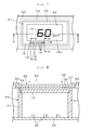
FIG. 1 is a front view of a liquid crystal display device according to an embodiment of the present invention.
FIG. 2 is a sectional view taken along a line A-A of FIG. 1.
FIG. 3 is a magnified sectional view of a liquid crystal display element in FIG. 2.
FIG. 4 is a front view of a lower glass substrate provided with first and second lead terminals, the lead terminals of the same embodiment.
FIG. 5 is a sectional view taken along a line C-C of FIG. 1.
FIG. 6 is a sectional view taken along a line D-D of FIG. 1.
FIG. 7 is a sectional view showing essential parts of a liquid crystal display device according to a modification of the same embodiment.
DESCRIPTION OF EMBODIMENTS
Hereinafter, an explanation will be given of an embodiment of the present invention applied to a digital speed meter installed in a vehicle instrument, for example, with reference to the FIG. 1 to FIG. 6.
In FIG. 1 and FIG. 2, a digital speed meter as a liquid crystal display device according to the embodiment comprises a liquid crystal display element 10, a circuit board 20 that is disposed behind the liquid crystal display element 10 and is conductively connected to the liquid crystal display element 10 through a lead terminal 16 that is a connection member to be described later, a light source 30 mounted on the circuit board 20, a case body 40 disposed between the liquid crystal display element 10 and circuit board 20, a display panel (a front panel) 50 disposed in front of the liquid crystal display element 10 so as to cover the liquid crystal display element 10, and a flap member 60 to cover a peripheral edge of the display panel 50.
As shown in FIG. 3, the liquid crystal display element 10 is configured to connect the peripheries of the upper insulting substrate 11 and lower insulating substrate 12 with a sealing material 13, and to seal a liquid crystal 14 between the insulating substrates 11 and 12 more inside the sealing material 13. The insulating substrates 11 and 12 are made of rectangular transparent glass substrates. An upper polarizing plate (not shown) is provided on the upper surface of the upper insulating substrate 11, and a lower polarizing plate (not shown) is provided on the lower surface of the lower insulating substrate 12.
A first transparent electrode 11 a that is a transparent electrode having a predetermined shape is provided on the inside surface of the upper insulating substrate 11 (namely, on the surface of the upper insulating substrate 11 opposing the lower insulating substrate 12). A second transparent electrode 12 a that is a transparent electrode having a predetermined shape is provided on the inside surface of the lower insulating substrate 12 (namely, on the surface of the lower insulating substrate 12 opposing the upper insulating substrate 11) so as to oppose (correspond to) the first transparent electrode 11 a.
The first transparent electrode 11 a and second transparent electrode 12 a are arranged on the inside surfaces of the insulating substrates 11 and 12 so as to hold the liquid crystal 14. The planar shapes of the transparent electrodes seem substantially the same from a viewer (when looking straight at the liquid crystal display device). The portions of the display surface area of the liquid crystal display element 10 corresponding to the first transparent electrode 11 a and second transparent electrode 12 a form a display portion 15 that forms a display pattern. In other words, this means that the display portion 15 is formed by providing the transparent electrodes 11 a and 12 a on the inside surfaces of the insulating substrates 11 and 12, respectively, so as to face each other.
Of the upper insulating substrate 11 and lower insulating substrate 12, in the lower insulating substrate 12, a plurality of metal lead terminals 16 is fixed along one end edge. In this embodiment, each lead terminal 16 is centrally provided in a part of one end edge of the lower insulating substrate 12, thereby conductively connecting the liquid crystal display element 10 and circuit board 20.
Although a detailed illustration is omitted, the shape of each lead terminal 16 is substantially the same as the shape of a second lead terminal to be described later. The lead terminal 16 has a holding part and a lead portion. The holding part of the lead terminal 16 is formed in a U-shape, and is electrically connected to the second transparent electrode 12 a when it holds the end of the lower insulating substrate 12. The end portion of the lead terminal 16 is electrically connected to a wiring (not shown) provided in the circuit board
When a voltage corresponding to an external measurand is applied across the transparent electrodes 11 a and 12 a through the lead terminal 16, a measurand (for example, a vehicle speed) corresponding to a vehicle operating state is digitally displayed black in the display portion 15. In the liquid crystal display element 10, the background area 15 a except the display portion 15 is illuminated by lighting of the light source 30 mounted on the circuit board 20.
Of the insulating substrates 11 and 12, on the inside surface of the lower insulating substrate 12, a conductive part 17 comprising a substantially frame-shaped conductive pattern is formed so as to surround the second transparent electrode 12 a. The conductive part 17 is formed in a substantially frame shape on the inside surface of the lower insulating substrate 12 so as to avoid the disposed position of the lead terminal 16 (see FIG. 4). In FIG. 4, the transparent electrode 12 a is formed inside the conductive part 17 (in the substantially central area of the lower insulating substrate 12), but an illustration of the transparent electrode 12 a is omitted.
In particular, the conductive part 17 comprises a first conductive pattern T1 whose one end side is conductively connected to a first grounding terminal to be described later and the other end side is located between the first grounding terminal and transparent electrode 12 a, a second conductive pattern T2 that is formed by routing from the first conductive pattern T1 opposite to the part connected to the first grounding terminal to the right side of the lower insulating substrate 12, a third conductive pattern T3 that is formed by routing along the right end surface of the lower insulating substrate 12, a fourth conductive pattern T4 that is formed by routing along the upper end surface of the lower insulating substrate 12, a fifth conductive pattern T5 that is formed by routing along the left end surface of the lower insulating substrate 12, a sixth conductive pattern T6 that extends from the lower end of the fifth conductive pattern T5 toward the second conductive pattern T2 without contacting the second conductive pattern T2, and a seventh conductive pattern T7 that conductively connects the sixth conductive pattern T6 and second grounding terminal to be described later.
Further, on the right side of each lead terminal 16, a first grounding terminal 18 that is a first grounding part is provided in the lower insulating substrate 12 a state of being juxtaposed with each lead terminal 16. The first grounding terminal 18 is made of metal material like each lead terminal 16, and has a holding part 18 a conductively connected to the first conductive pattern T1 of the conductive part 17, and a contact piece 18 b formed by bending in a substantially U-shape (see FIG. 5).
The holding part 18 a is formed in a substantially U-shape, and is electrically connected to the first conductive pattern T1 by holding the end of the lower insulating substrate 12. On the other hand, the contact piece 18 b is configured so that its distal end side contacts (abuts) the back of a display panel 50 (a ground color part 52), and has a function of propagating static electricity charged in the display panel 50 to the conductive part 17 (the first conductive pattern T1) through the holding part 18 a of the first grounding terminal 18.
In other words, in this embodiment, the first grounding terminal 18 is configured so that one end side that is the holding part 18 a is conductively connected to the first conductive pattern T1 of the conductive part 17, and the other end side that is a front end of the contact piece 18 b abuts the display panel 50.
On the other hand, on the left side of each lead terminal 16 that is the opposite side to the first grounding terminal 18, the second grounding terminal 19 that is the second grounding part is provided in the lower insulating substrate 12 a state of being juxtaposed with each lead terminal 16. The second grounding terminal 19 is made of metal material like each lead terminal 16 and first lead terminal 18, and has a holding part 19 a of the same shape as the holding part 18 a of the first grounding terminal 18, and a linear lead part 19 b formed by suspending downward the holding part 19 a (namely, toward the circuit board 20) (see FIG. 6).
The holding part 19 a is formed in a substantially U-shape, and is electrically connected to the seventh conductive pattern T7 of the conductive part 17 by holding the end of the lower insulating substrate 12. On the other hand, the front end of the lead part 19 b that is located opposite to the holding part 19 a is electrically connected to a grounding part to be described later provided in the circuit board 20.
In other words, in this embodiment, the second grounding terminal 19 is configured so that one end side that is the holding part 19 a is conductively connected to the seventh conductive pattern T7 of the conductive part 17, and the other end that is a front end of the lead part 19 b is conductively connected to the grounding part.
Therefore, when the display panel 50 electrostatically charged, the static electricity charged in the display panel 50 propagates to the conductive part 17 (namely, propagates sequentially to the first to seventh conductive patterns T1 to T7) through the contact piece 18 b and holding part 18 a of the first grounding terminal 18, and then flows to the grounding part provided in the circuit board 20 through the holding part 19 a and lead part 19 b of the second grounding terminal 19 that is conductively connected to the seventh conductive pattern T7 (see FIG. 4 to FIG. 6).
The circuit board 20 is made of a rigid circuit board provided with a wiring pattern that is the wiring part formed on a glass epoxy resin base material, for example, in which the wiring part is conductively connected to a light source 30, an element driving circuit (not shown) to drive the liquid crystal display element 10, and various circuit components such as a resistor and a capacitor (not shown).
A reference numeral 21 denotes a grounding part comprising a grounding pattern provided on the front surface of the circuit board 20. The grounding part 21 is conductively connected to the lead part 19 b of the second grounding terminal 19. In this case, a hole 22 penetrating the front and back of the circuit board 20 is provided at a portion of the circuit board 20 corresponding to the lead part 19 b, and the front end of the lead part 19 b penetrates through the hole 22, and projects to the back of the circuit board 20. In other words, the grounding part 21 is formed as a pattern on the front (or back) of the circuit board 20 that is a periphery of the hole 22, and is electrically connected to the lead part 19 b by soldering or the like.
The light source 30 is comprised of a chip type light-emitting diode to emit an appropriate color, for example, and is comprised of a light-emitting body, which is mounted on the wiring part provided on the circuit board 20, and supplies illumination light to the liquid crystal display element 10. The illumination light from the light source 30 illuminates the background area 15 a except the display portion 15 by transmitting through there.
The case body 40 is made of white synthetic resin, for example, and has a function as a supporter to support the liquid crystal display element 10 and display panel 50, a function as a reflector to reflect the illumination light from the light source 30 to the liquid crystal display element 10, and a function as a terminal holder to guide and hold each lead terminal 16 and second grounding terminal 19.
Such a case body 40 comprises a substantially frame-shaped base part 41 to support the liquid crystal display element 10 and display panel 50, a plurality of terminal holders 42 to guide and hold each lead terminal 16 and second grounding terminal 19, and a connection part 43 to connect the base part 41 and terminal guide 42, which are formed in one body.
Each terminal holder 42 is formed substantially in a frame shape, and is configured to guide the lead part of each lead terminal 16 and the lead part 19 b of the second grounding terminal 19. FIG. 6 shows only the terminal holder 42 corresponding to the lead part 19 b of the second grounding terminal 19. It is needless to say that the terminal holder 42 corresponding to the lead part of each lead terminal 16 has the same shape as the lead part 19 b.
The display panel 50 comprises a design panel provided with a display design such as an indicator display portion (not shown), and uses a light-transmissive substrate 51 made of polycarbonate as a base material. On the back of the light-transmissive substrate 51, a ground color part 52 made of a blacked print layer is formed by printing using a means of screen printing, etc.
In this case, in the central area of the ground color part 52 corresponding to the display portion 15 of the liquid crystal display element 10, a substantially rectangular through portion 53, which is a vent print part where the black printed layer forming the ground color part 52 is not formed, is provided. Therefore, when a viewer looks straight at the liquid crystal display device from the front side of the liquid crystal display device, a viewer can see (visually recognize) display of the display portion 15 of the liquid crystal display element 10 through the through portion 53 provided in the display panel 50.
Further, in this case, a clearance between the through portion 53 formed in the central area of the display panel 50 and the liquid crystal display element 10 (the upper insulating substrate 11) disposed behind the display panel 50 (the through portion 53) so as to be parallel to the display panel 50 should be set to several millimeters. The base color part 52 may be formed by printing on the front surface of the light-transmissive substrate 51, not on the back of the light-transmissive substrate 51, or the display panel 50 may be formed as a panel body not provided with the display design. Further, if necessary, a diffusing plate (not shown) for evenly diffusing the illumination light from the light source 30 may be provided between the display panel 50 and circuit board 20.
The flap member 60 is made of black synthetic resin, for example, and is disposed on the display panel 50 so as to cover essential parts of the display panel 50, and is provided with an opening 61 comprised of an open window corresponding to the through portion 53.
The liquid crystal display device comprises the parts described above. In such a configuration, static electricity charged on the display panel 50 (the light-transmissive substrate 51) when a human hand touches the area near the center of the front surface of the through portion 53 of the display panel 50, for example, sequentially propagates to the contact piece 18 b abutting the display panel 50 and the holding part 18 a of the first grounding terminal 18, the first conductive pattern T1 that is a predetermined portion of the conductive part 17, second conductive pattern T2, third conductive pattern T3, fourth conductive pattern T4, fifth conductive pattern T5 and sixth conductive pattern T6, which are predetermined parts of the conductive part 17, the seventh conductive pattern T7 that is the other portion of the conductive part 17 different from the predetermined portion, and the holding part 19 a and lead part 19 b of the second grounding terminal 19, and then positively flows finally to the grounding part 21 that is a grounding pattern of the circuit board 20 conductively connected to the lead part 19 b. This suppresses the element driving circuit from being damaged by static electricity, and eliminates the possibility of malfunction (display error) of the liquid crystal display element 10 under the influence of static electricity, thereby providing a liquid crystal display device with improved display quality.
As described above, in this embodiment, a liquid crystal display device comprises a liquid crystal display element 10 that forms a display portion 15 by providing transparent electrodes 11 a and 12 a on the inside surface of a pair of insulating substrates 11 and 12 sealing a liquid crystal 14, a circuit board 20 that is conductively connected to the liquid crystal display element 10 through a plurality of metal lead terminals 16, and a conductive part 17 formed so as to surround the transparent electrode 12 a, wherein the the conductive part 17 is provided on one insulating substrate 12 so as to avoid a disposed position of the lead terminal 16, the liquid crystal display device comprising a display panel 50 having an through portion 53 that enables visual recognition of the display portion 15, a first grounding terminal 18 whose one end side is conductively connected to a first conductive pattern T1 of the conductive part 17 and the other end side abuts the display panel 50, and a second grounding terminal 19 whose one end side is conductively connected to a conductive pattern T7 of the conductive part 17 and the other end side is conductively connected to a grounding part 21 provided on the circuit board 20. A plurality of lead terminals 16 that are connecting members is provided on the lower insulating substrate 12 so as to conductively connect the liquid crystal display element 10 and circuit board 20, and the second grounding terminals 18 and 19 that are first and second grounding parts are provided on the lower insulating substrate 12 in a state of being juxtaposed with each lead terminal 16.
Therefore, static electricity charged in the display panel 50 when a human hand touches the area near the center of the front surface of the through portion 53 propagates to the contact piece 18 b contacting (abutting) the display panel of the first grounding terminal 18 without propagating to the liquid crystal display element 10, and the static electricity propagated to the contact piece 18 b propagates to the conductive part 17 comprised of conductive patterns and formed so as to surround the display portion 15 through the holding part 18 a. And, the static electricity propagated to the conductive part 17 positively flows finally to the grounding part 21 comprised of grounding patterns and conductively connected to the lead part 19 b through the holding part 19 a and lead part 19 b of the second grounding terminal 19 conductively connected to the conductive part 17. This eliminates the possibility of malfunction of the liquid crystal display element 10 under the influence of static electricity, thereby providing a liquid crystal display device with improved display quality.
Further, in this embodiment, an explanation has been given of the aspect that the contact piece 18 b located in the other end side of the first grounding terminal 18 is formed by bending in a U-shape so as to abut the display panel 50. However, the contact piece 18 b can be formed in any shape able to contact (abut) the display panel 50, for example, the contact piece 18 b can be formed in a spiral (helical) shape or in zigzag (S-shape).
Further, the contact piece 18 b located in the other end side of the first grounding terminal 18 is desirably configured to always abut the display panel 50 in a state of having elasticity to give a tension (a pressing elastic force) to the display panel. As the contact piece 18 b abuts the display panel 50 in a state of having elasticity, the connection reliability between the first grounding terminal 18 and display panel 50 can be improved.
Further, in this embodiment, an explanation has been given of the aspect that the through portion 53 that enables viewing of the display portion 15 is formed in a part of the display panel 50 corresponding to the display portion 15. However, though a detailed illustration is omitted, it may be permitted to provide a penetrated portion consisting of a substantially rectangular through-hole in a part of the display panel 50 (namely, a part of the light-transmissive substrate 51) corresponding to the display portion 15, thereby enabling a viewer to visually recognize the display of the display portion 15 through the penetrated portion. At this time, the ground color part 52 may be provided in the back (or the front) of the light-transmissive substrate 51 except the penetrated portion.
Further, in this embodiment, an explanation has been given of the aspect that the first grounding terminal 18 is comprised of a holding part 18 a, and a contact piece 18 b. However, as shown in FIG. 7 illustrating a modification of the embodiment, the first grounding terminal 18 may be comprised of a holding part 18 a, a contact piece 18, and a linear connection part 18 c that is formed by suspending downward the holding part 18 a close to the circuit board 20, and the connection part 18 c may be conductively connected to the grounding part 21.
INDUSTRIAL APPLICABILITY
The present invention is applicable to a liquid crystal display device comprising a liquid crystal display element that forms a display portion by providing transparent electrodes on the inside surface of a pair of insulating substrates sealing a liquid crystal, and a circuit board that is conductively connected to the liquid crystal display element through a connection member comprised of a lead terminal.
DESCRIPTION OF REFERENCE NUMERALS
- 10 Liquid crystal display element
- 11 Upper insulating substrate (Insulating substrate)
- 11 a First transparent electrode (Transparent electrode)
- 12 Lower insulating substrate (Insulating substrate)
- 12 a Second transparent electrode (Transparent electrode)
- 14 Liquid crystal
- 15 Display portion
- 16 Lead terminal (Connection member)
- 17 Conductive part
- 18 First grounding terminal (First grounding part)
- 18 a, 19 b Holding part
- 18 b Contact piece
- 18 c Connection part
- 19 Second grounding terminal (Second grounding part)
- 19 b Lead part
- 20 Circuit board
- 21 Grounding part
- 40 Case body
- 50 Display panel (Front panel)
- 51 Light-transmissive substrate
- 53 Through portion
- 60 Flap member
- T1 First conductive pattern (Predetermined portion of conductive part)
- T2 Second conductive pattern
- T3 Third conductive pattern
- T4 Fourth conductive pattern
- T5 Fifth conductive pattern
- T6 Sixth conductive pattern
- T7 Seventh conductive pattern (Other portion of conductive part)