US9410233B2 - Method of manufacturing semiconductor device and wafer - Google Patents
Method of manufacturing semiconductor device and wafer Download PDFInfo
- Publication number
- US9410233B2 US9410233B2 US13/243,944 US201113243944A US9410233B2 US 9410233 B2 US9410233 B2 US 9410233B2 US 201113243944 A US201113243944 A US 201113243944A US 9410233 B2 US9410233 B2 US 9410233B2
- Authority
- US
- United States
- Prior art keywords
- tensile stress
- layer
- substrate
- polysilicon
- film
- Prior art date
- Legal status (The legal status is an assumption and is not a legal conclusion. Google has not performed a legal analysis and makes no representation as to the accuracy of the status listed.)
- Active - Reinstated, expires
Links
Images


Classifications
-
- C—CHEMISTRY; METALLURGY
- C23—COATING METALLIC MATERIAL; COATING MATERIAL WITH METALLIC MATERIAL; CHEMICAL SURFACE TREATMENT; DIFFUSION TREATMENT OF METALLIC MATERIAL; COATING BY VACUUM EVAPORATION, BY SPUTTERING, BY ION IMPLANTATION OR BY CHEMICAL VAPOUR DEPOSITION, IN GENERAL; INHIBITING CORROSION OF METALLIC MATERIAL OR INCRUSTATION IN GENERAL
- C23C—COATING METALLIC MATERIAL; COATING MATERIAL WITH METALLIC MATERIAL; SURFACE TREATMENT OF METALLIC MATERIAL BY DIFFUSION INTO THE SURFACE, BY CHEMICAL CONVERSION OR SUBSTITUTION; COATING BY VACUUM EVAPORATION, BY SPUTTERING, BY ION IMPLANTATION OR BY CHEMICAL VAPOUR DEPOSITION, IN GENERAL
- C23C14/00—Coating by vacuum evaporation, by sputtering or by ion implantation of the coating forming material
- C23C14/0021—Reactive sputtering or evaporation
- C23C14/0036—Reactive sputtering
-
- C—CHEMISTRY; METALLURGY
- C23—COATING METALLIC MATERIAL; COATING MATERIAL WITH METALLIC MATERIAL; CHEMICAL SURFACE TREATMENT; DIFFUSION TREATMENT OF METALLIC MATERIAL; COATING BY VACUUM EVAPORATION, BY SPUTTERING, BY ION IMPLANTATION OR BY CHEMICAL VAPOUR DEPOSITION, IN GENERAL; INHIBITING CORROSION OF METALLIC MATERIAL OR INCRUSTATION IN GENERAL
- C23C—COATING METALLIC MATERIAL; COATING MATERIAL WITH METALLIC MATERIAL; SURFACE TREATMENT OF METALLIC MATERIAL BY DIFFUSION INTO THE SURFACE, BY CHEMICAL CONVERSION OR SUBSTITUTION; COATING BY VACUUM EVAPORATION, BY SPUTTERING, BY ION IMPLANTATION OR BY CHEMICAL VAPOUR DEPOSITION, IN GENERAL
- C23C14/00—Coating by vacuum evaporation, by sputtering or by ion implantation of the coating forming material
- C23C14/0005—Separation of the coating from the substrate
-
- C—CHEMISTRY; METALLURGY
- C23—COATING METALLIC MATERIAL; COATING MATERIAL WITH METALLIC MATERIAL; CHEMICAL SURFACE TREATMENT; DIFFUSION TREATMENT OF METALLIC MATERIAL; COATING BY VACUUM EVAPORATION, BY SPUTTERING, BY ION IMPLANTATION OR BY CHEMICAL VAPOUR DEPOSITION, IN GENERAL; INHIBITING CORROSION OF METALLIC MATERIAL OR INCRUSTATION IN GENERAL
- C23C—COATING METALLIC MATERIAL; COATING MATERIAL WITH METALLIC MATERIAL; SURFACE TREATMENT OF METALLIC MATERIAL BY DIFFUSION INTO THE SURFACE, BY CHEMICAL CONVERSION OR SUBSTITUTION; COATING BY VACUUM EVAPORATION, BY SPUTTERING, BY ION IMPLANTATION OR BY CHEMICAL VAPOUR DEPOSITION, IN GENERAL
- C23C14/00—Coating by vacuum evaporation, by sputtering or by ion implantation of the coating forming material
- C23C14/06—Coating by vacuum evaporation, by sputtering or by ion implantation of the coating forming material characterised by the coating material
- C23C14/0641—Nitrides
-
- H01L21/28114—
-
- H01L21/28123—
-
- H01L21/32135—
-
- H01L21/32137—
-
- H01L29/42376—
-
- H—ELECTRICITY
- H10—SEMICONDUCTOR DEVICES; ELECTRIC SOLID-STATE DEVICES NOT OTHERWISE PROVIDED FOR
- H10D—INORGANIC ELECTRIC SEMICONDUCTOR DEVICES
- H10D64/00—Electrodes of devices having potential barriers
- H10D64/01—Manufacture or treatment
- H10D64/013—Manufacture or treatment of electrodes having a conductor capacitively coupled to a semiconductor by an insulator
- H10D64/01302—Manufacture or treatment of electrodes having a conductor capacitively coupled to a semiconductor by an insulator the insulator being formed after the semiconductor body, the semiconductor being silicon
- H10D64/01304—Manufacture or treatment of electrodes having a conductor capacitively coupled to a semiconductor by an insulator the insulator being formed after the semiconductor body, the semiconductor being silicon characterised by the conductor
- H10D64/01324—Manufacture or treatment of electrodes having a conductor capacitively coupled to a semiconductor by an insulator the insulator being formed after the semiconductor body, the semiconductor being silicon characterised by the conductor characterised by the sectional shape, e.g. T or inverted-T
-
- H—ELECTRICITY
- H10—SEMICONDUCTOR DEVICES; ELECTRIC SOLID-STATE DEVICES NOT OTHERWISE PROVIDED FOR
- H10D—INORGANIC ELECTRIC SEMICONDUCTOR DEVICES
- H10D64/00—Electrodes of devices having potential barriers
- H10D64/01—Manufacture or treatment
- H10D64/013—Manufacture or treatment of electrodes having a conductor capacitively coupled to a semiconductor by an insulator
- H10D64/01302—Manufacture or treatment of electrodes having a conductor capacitively coupled to a semiconductor by an insulator the insulator being formed after the semiconductor body, the semiconductor being silicon
- H10D64/01304—Manufacture or treatment of electrodes having a conductor capacitively coupled to a semiconductor by an insulator the insulator being formed after the semiconductor body, the semiconductor being silicon characterised by the conductor
- H10D64/01326—Aspects related to lithography, isolation or planarisation of the conductor
-
- H—ELECTRICITY
- H10—SEMICONDUCTOR DEVICES; ELECTRIC SOLID-STATE DEVICES NOT OTHERWISE PROVIDED FOR
- H10D—INORGANIC ELECTRIC SEMICONDUCTOR DEVICES
- H10D64/00—Electrodes of devices having potential barriers
- H10D64/20—Electrodes characterised by their shapes, relative sizes or dispositions
- H10D64/27—Electrodes not carrying the current to be rectified, amplified, oscillated or switched, e.g. gates
- H10D64/311—Gate electrodes for field-effect devices
- H10D64/411—Gate electrodes for field-effect devices for FETs
- H10D64/511—Gate electrodes for field-effect devices for FETs for IGFETs
- H10D64/517—Gate electrodes for field-effect devices for FETs for IGFETs characterised by the conducting layers
- H10D64/518—Gate electrodes for field-effect devices for FETs for IGFETs characterised by the conducting layers characterised by their lengths or sectional shapes
-
- H—ELECTRICITY
- H10—SEMICONDUCTOR DEVICES; ELECTRIC SOLID-STATE DEVICES NOT OTHERWISE PROVIDED FOR
- H10P—GENERIC PROCESSES OR APPARATUS FOR THE MANUFACTURE OR TREATMENT OF DEVICES COVERED BY CLASS H10
- H10P50/00—Etching of wafers, substrates or parts of devices
- H10P50/20—Dry etching; Plasma etching; Reactive-ion etching
- H10P50/26—Dry etching; Plasma etching; Reactive-ion etching of conductive or resistive materials
- H10P50/264—Dry etching; Plasma etching; Reactive-ion etching of conductive or resistive materials by chemical means
- H10P50/266—Dry etching; Plasma etching; Reactive-ion etching of conductive or resistive materials by chemical means by vapour etching only
- H10P50/267—Dry etching; Plasma etching; Reactive-ion etching of conductive or resistive materials by chemical means by vapour etching only using plasmas
- H10P50/268—Dry etching; Plasma etching; Reactive-ion etching of conductive or resistive materials by chemical means by vapour etching only using plasmas of silicon-containing layers
Definitions
- the present invention relates to semiconductor technology, and more particularly, to a method of manufacturing semiconductor device and a wafer.
- FIG. 8 is a graph showing the variation in NMOST (N-channel Metal-Oxide-Semiconductor Field-effect transistor) gate source/drain overlap capacitance as a function of the shape of a polysilicon gate (see Yung-Huei Lee, et al, IEDM 04-481 19.3.1).
- curve a, b and c respectively indicate the variations in gate source/drain overlap capacitance of a gate with reentrants on the bottom, a gate with a straight wall on the bottom and a gate with foot on the bottom.
- FIG. 9A-9B is a graph showing comparison of the NMOST
- FIG. 9A is a graph showing the variation in NMOST TDDB of area structure (30 ⁇ 15 ⁇ m 2 ) as a function of the shape of a polysilicon gate.
- 9B is a graph showing the variation in NMOST TDDB of edge structure (2000 ⁇ m ⁇ 60 nm) as a function of the shape of a polysilicon gate. Stresses are performed at different e-fields for the two structures. There is no significant difference in TDDB distribution of area structure between the three splits. However, for the edge structure, the mean time of failure (MTF) of the polysilicon gate with foot on the gate bottom shows about 2.5 ⁇ reduction than the other two splits.
- MTF mean time of failure
- the polysilicon gate with foot tends to cause more gate-to-LDD overlap, and brings larger device overlap capacitance; the polysilicon gate with foot allows high energy implant to penetrate through the edge of the gate oxide which may downgrade the reliability of the gate oxide, and cause polysilicon gate edge TDDB failure.
- prior art there is no process or method for controlling the producing of polysilicon gates with reentrants well.
- An object of the present invention is to provide a method of manufacturing semiconductor device for forming a polysilicon gate with reentrants.
- Another object of the present invention is to provide a wafer made for forming a polysilicon gate with reentrants.
- a method of manufacturing a semiconductor device includes: providing a substrate, on a first surface of which a gate oxide layer and a polysilicon layer are formed; etching the polysilicon layer by use of a patterned mask so as to form a polysilicon gate with reentrants; wherein the method further comprises: depositing a tensile stress film on a second surface of the substrate before etching the polysilicon layer.
- the method further includes: removing the tensile stress film after forming the polysilicon gate.
- the tensile stress film is a nitride film with a tensile stress.
- the tensile stress film is a titanium nitride film, a phosphorus nitride film, or an aluminium nitride film.
- the tensile stress film has a thickness of 2-50 nm.
- the substrate is formed with the gate oxide layer, the polysilicon layer and a hard mask layer on the first surface thereof.
- Depositing a tensile stress film on a second surface of the substrate before etching the polysilicon layer includes: depositing the tensile stress film on the second surface of the substrate before forming the hard mask layer on the first surface of the substrate; or depositing the tensile stress film on the second surface of the substrate, after patterning the hard mask layer, and before etching the polysilicon layer with the patterned hard mask layer.
- the substrate is formed with the gate oxide layer, the polysilicon layer and a photoresist layer on the first surface thereof.
- Depositing a tensile stress film on a second surface of the substrate before etching the polysilicon layer includes: depositing the tensile stress film on the second surface of the substrate before forming the photoresist layer on the first surface of the substrate; or depositing the tensile stress film on the second surface of the substrate, after patterning the photoresist layer by means of photolithography to form a patterned photoresist layer and before etching the polysilicon layer masked by the patterned photoresist layer.
- the etching is a dry etching or a plasma etching.
- the tensile stress film can be deposited on the second surface of the substrate for generating the tensile stress for the wafer.
- a polysilicon gate with reentrants can be formed in etching process.
- a wafer for manufacturing semiconductor device includes: a tensile stress film deposited on a surface of the wafer for producing a tensile stress on the wafer.
- the tensile stress film is a nitride film with tensile stress.
- a wafer with the tensile stress film on one of its surface is provided.
- the strain on the wafer caused by the tensile stress film is helpful to make a polysilicon gate with reentrants formed on the wafer.
- FIG. 1 is a flowchart schematically showing a method of manufacturing semiconductor device in accordance with a first embodiment of the present invention
- FIG. 2 is a flowchart schematically showing a method of manufacturing semiconductor device in accordance with a second embodiment of the present invention
- FIG. 3A-3F schematically illustrate sectional views of a semiconductor device of respective steps in the method of manufacturing semiconductor device in accordance with the second embodiment of the present invention
- FIG. 3A illustrates a sectional view after forming a gate oxide layer and a polysilicon layer in succession on the first surface of the substrate
- FIG. 3B illustrates a sectional view after depositing a TiN layer on the second surface of the substrate
- FIG. 3C illustrates a sectional view after forming a photoresist pattern on the polysilicon layer
- FIG. 3D illustrates a sectional view after forming a polysilicon gate with reentrants through etching the polysilicon layer using patterned photoresist as a mask
- FIG. 3E illustrates a sectional view after removing the remained photoresist
- FIG. 3F illustrates a sectional view after removing the TiN layer
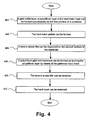
- FIG. 4 is a flowchart showing a method of manufacturing semiconductor device in accordance with a third embodiment of the present invention.
- FIG. 5A-5F schematically illustrate sectional views of a semiconductor device of respective steps in the method of manufacturing semiconductor device in accordance with the third embodiment of the present invention
- FIG. 5A illustrates a sectional view after forming a gate oxide layer, a polysilicon layer and a hard mask in succession on a first surface of the substrate
- FIG. 5B illustrates a sectional view after forming a hard mask pattern
- FIG. 5C illustrates a sectional view after depositing a TiN layer on a second surface of the substrate
- FIG. 5D illustrates a sectional view after forming a polysilicon gate with reentrants through etching the polysilicon layer using the patterned hard mask as a mask
- FIG. 5E illustrates a sectional view after removing the TiN layer
- FIG. 5F illustrates a sectional view after removing the remained hard mask
- FIG. 6 is a graph showing the corresponding relation between the thinkness of a TiN liner and stress
- FIG. 7A-7B is a diagram showing effects on the shape of a polysilicon gate caused by different stresses applied on the substrate by a screw and a tungsten wire;
- FIG. 7A illustrates situations of respectively applying a compressive stress (a) and a tensile stress (b) by a screw and tungsten wire;
- FIG. 7B illustrates the shapes of the polysilicon gates;
- FIG. 8 is a graph showing the variation in NMOST gate source/drain overlap capacitance as a function of the shape of a polysilicon gate
- FIG. 9A is a graph showing the variation in NMOST TDDB of area structure as a function of the shape of a polysilicon gate
- FIG. 9B is a graph showing the variation in NMOST TDDB of edge structure as a function of the shape of a polysilicon gate.
- FIG. 1 is a flowchart showing a method of manufacturing semiconductor device in accordance with a first embodiment of the present invention.
- a substrate is provided.
- a gate oxide layer and a polysilicon layer are formed on a first surface of the substrate.
- a tensile stress film can be deposited on a second surface of the substrate.
- the tensile stress film includes nitride films, such as, titanium nitride (TiN) film, phosphorus nitride film, aluminium nitride film etc.
- the step of depositing TiN includes: at room temperature or high temperature, the target (Ti) can be sputtered by plasma such as Ar, nitrogen can be brought into a chamber for depositing TiN. The content of nitrogen and the thinkness of TiN can affect the stress of TiN. In one embodiment, the thinkness of the tensile stress film can be 2-50 nm.
- the polysilicon layer is etched by use of a patterned mask so as to form a polysilicon gate with reentrants. Either a dry etching or a plasma etching can be adopted.
- FIG. 1 illustrates the step 104 being between the step 102 and the step 106
- the embodiment shown in FIG. 1 doesn't mean to limit the sequence of the step 104 .
- the object of the present invention can be achieved as long as the tensile stress film is deposited on the second surface of the substrate before etching the polysilicon.
- the sequence of the depositing the tensile stress film step in the process will be described next in various exemplary embodiments with reference to the drawings.
- a tensile stress can be applied on the wafer, so as to produce a polysilicon gate with reentrants by etching the polysilicon layer.
- semiconductor devices can have smaller gate-source/drain overlap capacitance and better TDDB parameters, and the performance of the semiconductor devices can be improved.
- FIG. 2 is a flowchart showing a method of manufacturing semiconductor device in accordance with a second embodiment of the present invention.
- a gate oxide layer and a polysilicon layer can be formed successively on a first surface of a substrate.
- a tensile stress film can be deposited on a second surface of the substrate. After depositing the tensile stress film, the tensile stress can be applied on the wafer.
- a photoresist layer can be formed on the polysilicon layer.
- the photoresist pattern can be formed by patterning the photoresist layer by means of photolithography.
- a polysilicon gate with reentrants can be formed by etching the polysilicon layer using a patterned photoresist as a mask. Under the tensile stress generated by the tensile stress film, the polysilicon gate with reentrants can be formed by etching the polysilicon layer. The dry etching process can be used.
- the remained photoresist can be removed.
- the tensile stress film can be removed.
- FIG. 3A-3F schematically illustrate sectional views of a semiconductor device of respective steps in the method of manufacturing semiconductor device in accordance with the second embodiment of the present invention
- FIG. 3A illustrates a sectional view after forming a gate oxide layer and a polysilicon layer in succession on the first surface of the substrate
- FIG. 3B illustrates a sectional view after depositing a TiN layer on the second surface of the substrate
- FIG. 3C illustrates a sectional view after forming a photoresist pattern on the polysilicon layer
- FIG. 3D illustrates a sectional view after forming a polysilicon gate with reentrants 31 through etching the polysilicon layer using patterned photoresist as a mask
- FIG. 3E illustrates a sectional view after removing the remained photoresist
- FIG. 3F illustrates a sectional view after removing the TiN layer.
- the TiN layer in the embodiments as shown in FIG. 2 and FIG. 3 can be deposited after forming the photoresist layer or forming the patterned photoresist, and before etching the polysilicon layer, even before forming the polysilicon layer; the sequence of the steps of removing the photoresist and the TiN layer can be exchanged; or the step of removing the TiN layer can be omitted.
- Other types of the tensile stress film can be used to replace the TiN layer in above embodiments according to requirements.
- the tensile stress film can be deposited on different occasions, so as to produce more choices and flexibility.
- FIG. 4 is a flowchart showing a method of manufacturing a semiconductor device in accordance with a third embodiment of the present invention.
- the polysilicon layer can be etched through a patterned hard mask.
- a gate oxide layer, a polysilicon layer and a hard mask layer can be formed successively on the first surface of a substrate.
- the hard mask pattern can be formed.
- the photoresist layer can be formed on the hard mask layer.
- the photoresist layer can be photoetched to form a patterned photoresist which can be used as a mask for etching the hard mask in order to form a hard mask pattern; non-photoetching methods can also be used to form the hard mask pattern.
- a tensile stress film can be deposited on the second surface of the substrate. After depositing the tensile stress film, the tensile stress can be applied on the wafer.
- a polysilicon gate with reentrants can be formed by etching the polysilicon layer by use of the patterned hard mask. Under the tensile stress generated by the tensile stress film, the polysilicon gate with reentrants can be formed by etching the polysilicon layer.
- the tensile stress film can be removed.
- the hard mask can be removed.
- FIG. 5A-5F schematically illustrate sectional views of a semiconductor device of respective steps in the method of manufacturing semiconductor device in accordance with the third embodiment of the present invention
- FIG. 5A illustrates a sectional view after forming a gate oxide layer, a polysilicon layer and a hard mask in succession on a first surface of a substrate
- FIG. 5B illustrates a sectional view after forming a hard mask pattern
- FIG. 5C illustrates a sectional view after depositing a TiN layer on a second surface of the substrate
- FIG. 5D illustrates a sectional view after forming a polysilicon gate with reentrants 51 through etching the polysilicon layer by use of the patterned hard mask
- FIG. 5E illustrates a sectional view after removing the TiN layer
- FIG. 5F illustrates a sectional view after removing the remained hard mask.
- the tensile stress film is deposited after forming the hard mask pattern, and the tensile stress film can be removed as soon as possible after etching the polysilicon layer. Therefore, it can be avoided that the tensile stress film affects other steps in the manufacturing process. And the pollution caused by the tensile stress film can be avoided.
- the TiN layer in the embodiments as shown in FIG. 4 and FIG. 5 can be deposited before forming the patterned hard mask, even before forming the polysilicon layer; the sequence of the steps of removing the hard mask and removing the TiN layer can be exchanged; or the step of removing the TiN layer can be omitted.
- Other types of the tensile stress film can be used to replace the TiN layer in above embodiments according to requirements.
- FIG. 6 is a graph showing the corresponding relation between the thickness of a TiN pad and stress. As shown in FIG. 6 , in a certain scope, a thinner film can generate bigger stress at the same thickness on the front surface of the substrate.
- the stress can be controlled by modifying the thickness of the tensile stress film, which can further control the size of the reentrants.
- the size of the reentrants can be controlled by modifying the thickness of the tensile stress film, which can further control the performance of semiconductor devices.
- a wafer for manufacturing semiconductor device is provided.
- a tensile stress film deposited on one surface of the wafer can generate tensile stress for the wafer.
- the tensile stress film can be a Nitride film with the tensile stress, for example, a titanium nitride (TiN) film, a phosphorus nitride film, a aluminum nitride film etc.
- Wafers with the tensile stress film can be provided for professional and mass production so as to improve the quality of semiconductor devices, and also avoid affecting other processes or causing pollution.
- the wafer successively includes: a substrate, a gate oxide layer, a polysilicon layer; a photoresist layer can also be included on the polysilicon layer.
- the wafer successively includes a substrate, a polysilicon layer and a hard mask layer; a buffer layer can be included between the polysilicon layer and the hard mask layer; a photoresist layer can also be included on the hard mask layer. Wafers with different layers can be used by users according to users' requirements, which provide more choices and flexibility for users.
- FIG. 7A-7B is a diagram showing effects on the shape of a polysilicon gate caused by different stresses applied on the substrate by a screw and a tungsten wire (see: Jane P. Chang, et al, J. Vac. Sci. Technol. B 19 (5), September/October 2001).
- FIG. 7A illustrates situations of applying a compressive stress (a) and a tensile stress (b) respectively by a screw 73 and a tungsten wire 71 .
- the label 71 indicates the tungsten wire
- the label 72 indicates a patterned poly sample
- the label 73 indicates the screw.
- FIG. 7B illustrates the shapes of the polysilicon gates.
- the polysilicon gate with reentrants on its bottom can be formed by depositing the tensile stress film on the back surface of the substrate.
Landscapes
- Chemical & Material Sciences (AREA)
- Chemical Kinetics & Catalysis (AREA)
- Engineering & Computer Science (AREA)
- Materials Engineering (AREA)
- Mechanical Engineering (AREA)
- Metallurgy (AREA)
- Organic Chemistry (AREA)
- Electrodes Of Semiconductors (AREA)
- Internal Circuitry In Semiconductor Integrated Circuit Devices (AREA)
- Metal-Oxide And Bipolar Metal-Oxide Semiconductor Integrated Circuits (AREA)
Abstract
Description
Claims (10)
Applications Claiming Priority (3)
| Application Number | Priority Date | Filing Date | Title |
|---|---|---|---|
| CN201110109825 | 2011-04-29 | ||
| CN201110109825.3A CN102760690B (en) | 2011-04-29 | 2011-04-29 | Manufacture method and wafer of semiconductor device |
| CN201110109825.3 | 2011-04-29 |
Publications (2)
| Publication Number | Publication Date |
|---|---|
| US20120273923A1 US20120273923A1 (en) | 2012-11-01 |
| US9410233B2 true US9410233B2 (en) | 2016-08-09 |
Family
ID=47055091
Family Applications (1)
| Application Number | Title | Priority Date | Filing Date |
|---|---|---|---|
| US13/243,944 Active - Reinstated 2034-09-28 US9410233B2 (en) | 2011-04-29 | 2011-09-23 | Method of manufacturing semiconductor device and wafer |
Country Status (2)
| Country | Link |
|---|---|
| US (1) | US9410233B2 (en) |
| CN (1) | CN102760690B (en) |
Families Citing this family (4)
| Publication number | Priority date | Publication date | Assignee | Title |
|---|---|---|---|---|
| CN103888886A (en) * | 2014-03-14 | 2014-06-25 | 上海先进半导体制造股份有限公司 | Manufacturing method for low-stress in-situ doped polycrystalline silicon films |
| CN109429157B (en) | 2017-08-28 | 2021-02-09 | 中芯国际集成电路制造(上海)有限公司 | Microphone and method for manufacturing the same |
| CN107611012B (en) * | 2017-08-31 | 2020-10-02 | 长江存储科技有限责任公司 | A kind of stress control method and structure of prefabricated back film |
| CN113078093B (en) * | 2021-03-24 | 2022-08-19 | 长江存储科技有限责任公司 | Method for manufacturing semiconductor device, profiling wafer |
Citations (10)
| Publication number | Priority date | Publication date | Assignee | Title |
|---|---|---|---|---|
| CN1177829A (en) | 1996-09-06 | 1998-04-01 | 特利康设备有限公司 | Method of forming layer |
| US6110571A (en) * | 1994-07-19 | 2000-08-29 | Sumitomo Metal Mining Co., Ltd. | Duplex coated steel composite products and method of manufacturing them |
| US20040262688A1 (en) | 2003-06-25 | 2004-12-30 | International Business Machines Corporation | METHOD OF MAKING A finFET HAVING SUPPRESSED PARASITIC DEVICE CHARACTERISTICS |
| US20060118824A1 (en) * | 2003-08-08 | 2006-06-08 | Sanken Electric Co., Ltd. | Semiconductor device with reduced leakage current, and method of fabrication |
| US20070018205A1 (en) * | 2005-07-21 | 2007-01-25 | International Business Machines Corporation | STRUCTURE AND METHOD FOR IMPROVED STRESS AND YIELD IN pFETS WITH EMBEDDED SiGe SOURCE/DRAIN REGIONS |
| JP2007073801A (en) | 2005-09-08 | 2007-03-22 | Seiko Epson Corp | Semiconductor device |
| US20070099369A1 (en) * | 2005-10-31 | 2007-05-03 | Semiconductor Manufacturing International (Shanghai) Corporation | Integration scheme method and structure for transistors using strained silicon |
| US20080050886A1 (en) * | 2006-08-23 | 2008-02-28 | Elpida Memory, Inc. | Method of producing semiconductor device |
| US20110070701A1 (en) * | 2009-09-18 | 2011-03-24 | Semiconductor Manufacturing International (Shanghai) Corporation | Integration scheme for strained source/drain cmos using oxide hard mask |
| US7923313B1 (en) | 2010-02-26 | 2011-04-12 | Eastman Kodak Company | Method of making transistor including reentrant profile |
-
2011
- 2011-04-29 CN CN201110109825.3A patent/CN102760690B/en active Active
- 2011-09-23 US US13/243,944 patent/US9410233B2/en active Active - Reinstated
Patent Citations (10)
| Publication number | Priority date | Publication date | Assignee | Title |
|---|---|---|---|---|
| US6110571A (en) * | 1994-07-19 | 2000-08-29 | Sumitomo Metal Mining Co., Ltd. | Duplex coated steel composite products and method of manufacturing them |
| CN1177829A (en) | 1996-09-06 | 1998-04-01 | 特利康设备有限公司 | Method of forming layer |
| US20040262688A1 (en) | 2003-06-25 | 2004-12-30 | International Business Machines Corporation | METHOD OF MAKING A finFET HAVING SUPPRESSED PARASITIC DEVICE CHARACTERISTICS |
| US20060118824A1 (en) * | 2003-08-08 | 2006-06-08 | Sanken Electric Co., Ltd. | Semiconductor device with reduced leakage current, and method of fabrication |
| US20070018205A1 (en) * | 2005-07-21 | 2007-01-25 | International Business Machines Corporation | STRUCTURE AND METHOD FOR IMPROVED STRESS AND YIELD IN pFETS WITH EMBEDDED SiGe SOURCE/DRAIN REGIONS |
| JP2007073801A (en) | 2005-09-08 | 2007-03-22 | Seiko Epson Corp | Semiconductor device |
| US20070099369A1 (en) * | 2005-10-31 | 2007-05-03 | Semiconductor Manufacturing International (Shanghai) Corporation | Integration scheme method and structure for transistors using strained silicon |
| US20080050886A1 (en) * | 2006-08-23 | 2008-02-28 | Elpida Memory, Inc. | Method of producing semiconductor device |
| US20110070701A1 (en) * | 2009-09-18 | 2011-03-24 | Semiconductor Manufacturing International (Shanghai) Corporation | Integration scheme for strained source/drain cmos using oxide hard mask |
| US7923313B1 (en) | 2010-02-26 | 2011-04-12 | Eastman Kodak Company | Method of making transistor including reentrant profile |
Non-Patent Citations (7)
| Title |
|---|
| "Effects of Film Stress Modulation Using TiN Metal Gate on Stress Engineering and Its Impact on Device Characteristics in Metal Gate/High-k Dielectric SOI FinFETs", by Chang Yong Kang, et al., IEEE Electron Device Letters, vol. 29, No. 5, May 2008, pp. 487-490. |
| "Implant Damage and Gate-Oxide-Edge Effects on Product Reliability", by Yung-Huei Lee, et al., IEDM 04-481, © 2004, IEEE, pp. 19.3.1-19.3.4. |
| "Notch formation by stress enhanced spontaneous etching of polysilicon", by Jane P. Chang, et al., J. Vac. Sci. Technol. B 19(5), Sep./Oct. 2001, pp. 1870-1873. |
| Chang et al. "Notch Formation by stress enhanced etching of Poilysilicon" J. Vac. Sci. Tech. B. 19(5) Sep. 2001. * |
| Kang et al. "Effects of Film Stress modulation using TiN" IEEE 0741-3106; Oct. 2008. * |
| Lee et al. "Implant Damage and Gate-Oxide Effects on Product Reliability" IEDM 04-481 19.3.1, (2004). * |
| Office Action from corresponding Chinese Patent Office, Appl. No. 201110109825.3, issued Nov. 4, 2013. |
Also Published As
| Publication number | Publication date |
|---|---|
| US20120273923A1 (en) | 2012-11-01 |
| CN102760690B (en) | 2014-04-09 |
| CN102760690A (en) | 2012-10-31 |
Similar Documents
| Publication | Publication Date | Title |
|---|---|---|
| US9768196B2 (en) | Flexible display apparatus, flexible display motherboard and method for manufacturing flexible display motherboard | |
| US9269820B2 (en) | Manufacturing method of polysilicon layer, and polysilicon thin film transistor and manufacturing method thereof | |
| CN104409518B (en) | Thin film transistor (TFT) and preparation method thereof | |
| US9410233B2 (en) | Method of manufacturing semiconductor device and wafer | |
| CN107564803B (en) | Etching method, process equipment, thin film transistor device and manufacturing method thereof | |
| US7514370B2 (en) | Compressive nitride film and method of manufacturing thereof | |
| US10680070B2 (en) | Trench gate manufacturing method | |
| US9711602B2 (en) | Method of making thin film transistor array and source/drain contact via-interconnect structures formed thereby | |
| CN100590815C (en) | Manufacturing method of semiconductor device | |
| WO2016084205A1 (en) | Columnar semiconductor device and method for manufacturing same | |
| US20140167126A1 (en) | Semiconductor device and method for manufacturing same | |
| JP5685351B1 (en) | Method for manufacturing columnar semiconductor device | |
| CN107195631B (en) | Method for adjusting threshold value of CMOS (complementary Metal oxide semiconductor) device and CMOS device | |
| CN107195585B (en) | Method for adjusting threshold value of CMOS (complementary Metal oxide semiconductor) device and CMOS device | |
| CN102376645A (en) | Forming method of CMOS (Complementary Metal-Oxide-Semiconductor Transistor) device stress film | |
| US9343471B2 (en) | Embedded flash memory | |
| TW540117B (en) | Method for improving the roughness of the sidewall of a polysilicon layer in an etching process | |
| US20190157454A1 (en) | Thin film transistor and manufacture method thereof | |
| CN103730341B (en) | Semiconductor device manufacturing method | |
| US9437498B2 (en) | Method for the formation of different gate metal regions of MOS transistors | |
| CN103730345B (en) | Semiconductor device manufacturing method | |
| CN107994070B (en) | Transistor and method of making the same | |
| Weiskittel | Fabrication of Sub-300 nm Fins at RIT by SADP | |
| CN103578952B (en) | Semiconductor device manufacturing method | |
| CN106328510A (en) | Metal gate forming method |
Legal Events
| Date | Code | Title | Description |
|---|---|---|---|
| AS | Assignment |
Owner name: SEMICONDUCTOR MANUFACTURING INTERNATIONAL (SHANGHA Free format text: ASSIGNMENT OF ASSIGNORS INTEREST;ASSIGNORS:MENG, XIAOYING;ZHOU, JUNQING;ZHANG, HAIYANG;REEL/FRAME:026965/0070 Effective date: 20110902 |
|
| STCF | Information on status: patent grant |
Free format text: PATENTED CASE |
|
| FEPP | Fee payment procedure |
Free format text: MAINTENANCE FEE REMINDER MAILED (ORIGINAL EVENT CODE: REM.); ENTITY STATUS OF PATENT OWNER: LARGE ENTITY |
|
| LAPS | Lapse for failure to pay maintenance fees |
Free format text: PATENT EXPIRED FOR FAILURE TO PAY MAINTENANCE FEES (ORIGINAL EVENT CODE: EXP.); ENTITY STATUS OF PATENT OWNER: LARGE ENTITY |
|
| STCH | Information on status: patent discontinuation |
Free format text: PATENT EXPIRED DUE TO NONPAYMENT OF MAINTENANCE FEES UNDER 37 CFR 1.362 |
|
| FP | Lapsed due to failure to pay maintenance fee |
Effective date: 20200809 |
|
| PRDP | Patent reinstated due to the acceptance of a late maintenance fee |
Effective date: 20220211 |
|
| FEPP | Fee payment procedure |
Free format text: PETITION RELATED TO MAINTENANCE FEES FILED (ORIGINAL EVENT CODE: PMFP); ENTITY STATUS OF PATENT OWNER: LARGE ENTITY Free format text: PETITION RELATED TO MAINTENANCE FEES GRANTED (ORIGINAL EVENT CODE: PMFG); ENTITY STATUS OF PATENT OWNER: LARGE ENTITY Free format text: SURCHARGE, PETITION TO ACCEPT PYMT AFTER EXP, UNINTENTIONAL (ORIGINAL EVENT CODE: M1558); ENTITY STATUS OF PATENT OWNER: LARGE ENTITY |
|
| MAFP | Maintenance fee payment |
Free format text: PAYMENT OF MAINTENANCE FEE, 4TH YEAR, LARGE ENTITY (ORIGINAL EVENT CODE: M1551); ENTITY STATUS OF PATENT OWNER: LARGE ENTITY Year of fee payment: 4 |
|
| STCF | Information on status: patent grant |
Free format text: PATENTED CASE |
|
| MAFP | Maintenance fee payment |
Free format text: PAYMENT OF MAINTENANCE FEE, 8TH YEAR, LARGE ENTITY (ORIGINAL EVENT CODE: M1552); ENTITY STATUS OF PATENT OWNER: LARGE ENTITY Year of fee payment: 8 |