US9401798B1 - Frequency domain multiplexer - Google Patents
Frequency domain multiplexer Download PDFInfo
- Publication number
- US9401798B1 US9401798B1 US14/332,341 US201414332341A US9401798B1 US 9401798 B1 US9401798 B1 US 9401798B1 US 201414332341 A US201414332341 A US 201414332341A US 9401798 B1 US9401798 B1 US 9401798B1
- Authority
- US
- United States
- Prior art keywords
- filter
- frequency
- signal
- circuit
- parallel
- Prior art date
- Legal status (The legal status is an assumption and is not a legal conclusion. Google has not performed a legal analysis and makes no representation as to the accuracy of the status listed.)
- Expired - Fee Related, expires
Links
Images


Classifications
-
- H—ELECTRICITY
- H03—ELECTRONIC CIRCUITRY
- H03H—IMPEDANCE NETWORKS, e.g. RESONANT CIRCUITS; RESONATORS
- H03H7/00—Multiple-port networks comprising only passive electrical elements as network components
- H03H7/46—Networks for connecting several sources or loads, working on different frequencies or frequency bands, to a common load or source
- H03H7/463—Duplexers
-
- H—ELECTRICITY
- H04—ELECTRIC COMMUNICATION TECHNIQUE
- H04L—TRANSMISSION OF DIGITAL INFORMATION, e.g. TELEGRAPHIC COMMUNICATION
- H04L5/00—Arrangements affording multiple use of the transmission path
- H04L5/02—Channels characterised by the type of signal
- H04L5/06—Channels characterised by the type of signal the signals being represented by different frequencies
- H04L5/08—Channels characterised by the type of signal the signals being represented by different frequencies each combination of signals in different channels being represented by a fixed frequency
-
- H—ELECTRICITY
- H04—ELECTRIC COMMUNICATION TECHNIQUE
- H04B—TRANSMISSION
- H04B1/00—Details of transmission systems, not covered by a single one of groups H04B3/00 - H04B13/00; Details of transmission systems not characterised by the medium used for transmission
- H04B1/005—Details of transmission systems, not covered by a single one of groups H04B3/00 - H04B13/00; Details of transmission systems not characterised by the medium used for transmission adapting radio receivers, transmitters andtransceivers for operation on two or more bands, i.e. frequency ranges
- H04B1/0053—Details of transmission systems, not covered by a single one of groups H04B3/00 - H04B13/00; Details of transmission systems not characterised by the medium used for transmission adapting radio receivers, transmitters andtransceivers for operation on two or more bands, i.e. frequency ranges with common antenna for more than one band
- H04B1/0057—Details of transmission systems, not covered by a single one of groups H04B3/00 - H04B13/00; Details of transmission systems not characterised by the medium used for transmission adapting radio receivers, transmitters andtransceivers for operation on two or more bands, i.e. frequency ranges with common antenna for more than one band using diplexing or multiplexing filters for selecting the desired band
-
- H—ELECTRICITY
- H04—ELECTRIC COMMUNICATION TECHNIQUE
- H04B—TRANSMISSION
- H04B1/00—Details of transmission systems, not covered by a single one of groups H04B3/00 - H04B13/00; Details of transmission systems not characterised by the medium used for transmission
- H04B1/02—Transmitters
- H04B1/04—Circuits
- H04B1/0475—Circuits with means for limiting noise, interference or distortion
Definitions
- RF communication devices Integration of many functions on a single chip, including fabricating analog and digital circuitry on the same die, is desirable in many applications of semiconductor technology including RF communication devices.
- RF communication devices such as a power amplifier (PA), a low-noise amplifier (LNA), impedance matching components, and the like, have been integrated onto a system on chip (SOC).
- PA power amplifier
- LNA low-noise amplifier
- SOC system on chip
- frequency domain multiplexers including diplexers, triplexers, and the like, remain as off-chip components in the RF device.
- an apparatus in an embodiment, includes an antenna, a first transceiver circuit, a second transceiver circuit, a first filter coupled between the antenna and the first transceiver circuit and configured to pass a first signal and attenuate a second signal, and a second filter coupled between the antenna and the second transceiver circuit and configured to pass the second signal and attenuate the first signal.
- the first signal has a first frequency and the second signal has a second frequency.
- the first transceiver circuit, the second transceiver circuit, and the first filter are integrated in a system on chip (SOC).
- the second filter is integrated in the SOC.
- the first filter includes a first parallel circuit having a first capacitor and a first inductor that are coupled to each other in parallel, and a second inductor coupled in series with the first parallel circuit.
- the first frequency is in a 5 GHz band for WiFiTM communication and the second frequency is in a 2.4 GHz band for Bluetooth® communication.
- a method in an embodiment, includes passing a first signal and attenuating a second signal by a first filter coupled between an antenna and a first transceiver circuit, passing the second signal and attenuating the first signal by a second filter coupled between the antenna and a second transceiver circuit.
- the first signal has a first frequency and the second signal has a second frequency.
- the first transceiver circuit, the second transceiver circuit, and the first filter are integrated in an SOC.
- the first filter includes a parallel circuit that is configured to have a maximum impedance value at the second frequency in order to attenuate the second signal.
- the second filter is disposed outside the SOC, a package element is coupled to the first filter and the second filter, and a third filter is coupled to the second transceiver circuit and the package element.
- the method further includes attenuating a second harmonic of the second signal using the third filter to prevent a propagation of the second harmonic through the package element to a transmission path of the first signal.
- the first frequency is in a 5 GHz band for WiFiTM communication and the second frequency is in a 2.4 GHz band for Bluetooth® communication.
- FIG. 1 is a block diagram of a wireless device including a plurality of transceiver circuits that operate in multiple communication bands according to an embodiment.
- FIG. 2 is a block diagram of a portion of the wireless device of FIG. 1 including an SOC that has two transceiver circuits and two filters, according to an embodiment.
- FIG. 3A is a first circuit diagram of the portion of FIG. 2 , according to an embodiment.
- FIG. 3B is a second circuit diagram of the portion of FIG. 2 , according to an embodiment.
- FIG. 4A is a third circuit diagram of the portion of FIG. 2 , according to an embodiment.
- FIG. 4B illustrates elements of the portion 4 - 105 of FIG. 4A used to perform 5 GHz communication, according to an embodiment.
- FIG. 4C illustrates elements of the portion 4 - 105 of FIG. 4A used to perform 2.4 GHz communication, according to an embodiment.
- FIG. 5 is a block diagram of a portion of the wireless device of FIG. 1 including an off-chip filter and an SOC that has two transceiver circuits and a diplexer including one on-chip filter and one off-chip filter, according to an embodiment.
- FIG. 6A illustrates propagation of a second harmonic of a second signal to a transmission path of a first signal through a package element in the portion of FIG. 5 , according to an embodiment.
- FIG. 6B is a circuit diagram of a system including an off-chip filter and an SOC that has two transceiver circuits and two on-chip filters, according to an embodiment.
- FIG. 7 is a flowchart of a method of sharing an antenna to transmit or receive signals having different frequencies according to an embodiment.
- FIGS. 8A and 8B are flowcharts of a method of passing the first signal by the first filter of FIG. 7 and attenuating the first signal by the second filter of FIG. 7 , according to an embodiment.
- FIG. 1 is a block diagram of a wireless device 100 that communicates in multiple communication bands according to an embodiment.
- the wireless device 100 includes a first transceiver circuit 1 - 130 that handles signals in 5 GHz band, for example, signals having frequencies between 4.9 GHz and 5.9 GHz, for WiFiTM communication, and a second transceiver circuit 1 - 150 that handles signals in 2.4 GHz band, for example, signals having frequencies between 2.4 and 2.5 GHz, for Bluetooth® communication.
- the wireless device 100 also includes a third transceiver circuit 170 that handles signals in cellular telephone bands, for example, 850 MHz, 900 MHz, 1900 MHz, 2100 MHz bands, and the like. If desired, the wireless device 100 may also include any other suitable transceiver circuits.
- the first, second, and third transceiver circuits 1 - 130 , 1 - 150 , and 170 use a shared antenna 1 - 110 to transmit or receive signals.
- the size of the wireless device 100 may be reduced compared to using a separate antenna for each of the first, second, and third transceiver circuits 1 - 130 , 1 - 150 , and 170 .
- FIG. 2 is a block diagram of a portion of a wireless device 2 - 105 , corresponding to the portion 1 - 105 of the wireless device 100 of FIG. 1 , and including an System On a Chip (SOC) 2 - 210 and an antenna 2 - 110 according to an embodiment.
- the SOC 2 - 210 has first and second transceiver circuits 2 - 130 and 2 - 150 , and first and second filters 2 - 120 and 2 - 140 configured to operate together as a diplexer, e.g., an on-chip diplexer.
- a diplexer e.g., an on-chip diplexer.
- the first transceiver circuit 2 - 130 transmits and receives signals in a first frequency band, which in this embodiment includes 5 GHz band radio-frequency signals for WiFi communication.
- the second transceiver circuit 2 - 150 transmits and receives signals in a second frequency band different from the first frequency band, which in this embodiment includes 2.4 GHz band radio-frequency signals for Bluetooth communication.
- the first and second frequency bands do not overlap.
- the first and second transceiver circuits 2 - 130 and 2 - 150 share the same antenna 2 - 110 that is suitable for handling signals in both the first and second frequency bands.
- the first filter 2 - 120 couples the first transceiver circuit 2 - 130 to the antenna 2 - 110 and the second filter 2 - 140 couples the second transceiver circuit 2 - 150 to the antenna 2 - 110 , in order to allow the first and second transceiver circuits 2 - 130 and 2 - 150 to share the antenna 2 - 110 .
- the first filter 2 - 120 passes the first signals while the second filter 2 - 140 blocks the first signals.
- the first signals in the first frequency band are received or transmitted by the first transceiver 2 - 130 , but are not received or are received at a highly-attenuated signal level by the second transceiver 2 - 150 .
- the second filter 2 - 140 passes the second signals while the first filter 2 - 120 blocks the second signals.
- the second signals in the second frequency band are received or transmitted by the second transceiver 2 - 150 , but are not received or are received at a highly-attenuated signal level by the first transceiver 2 - 130 .
- the first filter 2 - 120 includes high-pass filter or a band-pass filter that passes the frequencies in the first frequency band and blocks or substantially attenuates frequencies in the second frequency band.
- the second filter 2 - 140 may include a low-pass filter or a band-pass filter that passes the frequencies in second frequency band and blocks or substantially attenuates frequencies in the first frequency band.
- the first filter 2 - 120 includes a band stop filter that substantially attenuates signals in the second frequency band.
- the second filter 2 - 140 may include a band stop filter that substantially attenuates signals in the first frequency band.
- each of the first and second filters 2 - 120 and 2 - 140 includes one or more of an appropriate band stop filter, band pass filter, high pass filter, and low pass filter.
- each of the first and second filters 2 - 120 and 2 - 140 may include only passive filters, for example, filters comprising only passive components such as inductors, capacitors, resistors, and the like.
- FIG. 3A is a first circuit diagram of a portion 3 - 105 a of a wireless device including an SOC 3 - 210 a and an antenna 3 - 110 a according to an embodiment.
- the SOC 3 - 210 has first and second transceiver circuits 3 - 130 a and 3 - 150 a , and first and second filters 3 - 120 a and 3 - 140 a.
- the first filter 3 - 120 a includes a first parallel LC circuit 3 - 310 a that has a first inductor 3 - 312 a and a first capacitor 3 - 311 a , and a second inductor 3 - 313 a coupled to the first parallel LC circuit 3 - 310 a in series.
- L 1 denotes an inductance value measured in henries of the first inductor 3 - 312 a
- C 1 denotes a capacitance value measured in farads of the first capacitor 3 - 311 a
- a first resonant frequency f 1 measured in hertz of the first parallel LC circuit 3 - 310 a is expressed as follows:
- the first parallel LC circuit 3 - 310 a has the first resonant frequency f 1 that is substantially equal to a frequency in the 2.4 GHz band.
- the total impedance of the first parallel LC circuit 3 - 310 a has a maximum value, and therefore for a signal having the first resonant frequency f 1 , a current flowing through the first parallel LC circuit 3 - 310 a is minimized.
- the first filter 3 - 120 a including the first parallel LC circuit 3 - 310 a becomes substantially open and stops or highly attenuates 2.4 GHz band radio-frequency signals.
- the first parallel LC circuit 3 - 310 a When 5 GHz band radio-frequency signals for WiFi communication are transmitted to the first parallel LC circuit 3 - 310 a , an inductive reactance of the first inductor 3 - 312 a increases and a capacitive reactance of the first capacitor 3 - 311 a decreases with the increase in frequency. As a result, the first parallel LC circuit 3 - 310 a presents a predominantly capacitive impedance, and thus the first filter 3 - 120 a becomes equivalent to a series LC circuit including the first capacitor 3 - 311 a and the second inductor 3 - 313 a.
- a second resonant frequency f 2 in hertz of the first filter 3 - 120 a is expressed as follows:
- the first filter 3 - 120 a acting as the series LC circuit has the second resonant frequency f 2 that is substantially equal to a frequency within the 5 GHz band.
- the a total impedance of the first filter 3 - 120 a has a minimum value, and therefore for a signal having the second resonant frequency f 2 a current flowing through the first parallel LC circuit 3 - 310 a is maximized.
- the first filter 3 - 120 a becomes substantially a short and passes 5 GHz band signals with a minimum amount of attenuation.
- a passband of the first filter 3 - 120 a ranges from 4.9 GHz to 5.9 GHz.
- a stopband of the first filter 3 - 120 a ranges from 2.4 GHz to 2.5 GHz.
- the second filter 3 - 140 a includes a second parallel LC circuit 3 - 330 a that has a third inductor 3 - 331 a and a third capacitor 3 - 332 a , and a second capacitor 3 - 333 a coupled to the second parallel LC circuit 3 - 330 a in series.
- L 3 denotes an inductance value in henries of the third inductor 3 - 331 a
- C 3 denotes a capacitance value in farads of the third capacitor 3 - 332 a
- a third resonant frequency f 3 in hertz of the second parallel LC circuit 3 - 330 a is expressed as follows:
- the second parallel LC circuit 3 - 330 a has the third resonant frequency f 3 that is substantially equal to a frequency in the 5 GHz band.
- a current flowing through the second parallel LC circuit 3 - 330 a is minimum.
- the second filter 3 - 140 a including the second parallel LC circuit 3 - 330 a becomes substantially open and stops or substantially attenuates 5 GHz band signals.
- a fourth resonant frequency f 4 in hertz of the second filter 3 - 140 a is expressed as follows:
- the second filter 3 - 140 a acting as the series LC circuit has the fourth resonant frequency f 4 that is substantially equal to a frequency in the 2.4 GHz band.
- a current flowing through the second filter 3 - 140 a is a maximum.
- the second filter 3 - 140 a becomes substantially a short and passes 2.4 GHz signals with a minimum amount of attenuation.
- a passband of the second filter 3 - 140 a ranges from 2.4 GHz to 2.5 GHz.
- the first filter 3 - 120 a passes 5 GHz band signals for WiFiTM Communication and stops 2.4 GHz band signals for Bluetooth® communication, while the second filter 3 - 140 a passes the 2.4 GHz band signals and stops the 5 GHz band signals.
- the first and second filters 3 - 120 a and 3 - 140 a allow the first and second transceivers 3 - 130 a and 3 - 150 a to share the same antenna 3 - 110 a for both of 5 GHz band WiFiTM communication and 2.4 GHz band Bluetooth® communication.
- the first and second filters 3 - 120 a and 3 - 140 a are integrated into the SOC 3 - 210 a .
- Such integration may lead to coupling issues between components of the filters 3 - 120 a and 3 - 140 a , for example, interference between the inductors 3 - 312 a , 3 - 313 a , and 3 - 331 a , change in transfer functions of the filters 3 - 120 a and 3 - 140 a , and the like.
- the first and second filters 3 - 120 a and 3 - 140 a may be spaced apart from each other at a predetermined distance.
- a closed metal ring is disposed around at least one of the inductors 3 - 312 a , 3 - 313 a , and 3 - 331 a .
- at least one of inductors 3 - 312 a , 3 - 313 a , and 3 - 331 a is an inductor having an upper loop and a lower loop connected together at the middle of the inductor so that current flowing in a clockwise direction in one loop flows in a counter-clockwise direction in the other loop.
- FIG. 3B is a second circuit diagram of a portion 3 - 105 b including an SOC 3 - 210 b and an antenna 3 - 110 b , according to an embodiment. Elements of the portion 3 - 105 b correspond to similarly-numbered elements of the portion 3 - 105 a of FIG. 3A .
- the portion 3 - 105 b differs from the portion 3 - 105 a by addition of a fourth inductor 351 .
- the fourth inductor 351 is coupled to a second capacitor 3 - 333 b to provide an alternative path for protecting the second capacitor 3 - 333 b from damage caused by electrostatic discharge (ESD).
- ESD electrostatic discharge
- an inductance value of the fourth inductor 351 and a capacitance value of the second capacitor 3 - 333 b is selected so that a second filter 3 - 140 b including a second parallel LC circuit 3 - 330 b and a third parallel LC circuit 350 operates in substantially the same manner as the second filter 3 - 140 a of FIG. 3A .
- the second filter 3 - 140 b passes 2.4 GHz radio-frequency signals and stops 5 GHz radio-frequency signals.
- FIG. 4A is a third circuit diagram of a portion 4 - 105 including an SOC 4 - 210 and an antenna 4 - 110 , according to an embodiment. Elements of the portion 4 - 105 having reference characters of the form “4-XXX” correspond to similarly-numbered elements of the portion 3 - 105 a of FIG. 3A .
- the portion 4 - 105 differs from the portion 3 - 105 a by addition of a second capacitor 411 , a third capacitor 413 , and a fifth capacitor 415 .
- the first capacitor 411 is coupled to a first terminal of a first parallel LC circuit 4 - 310 and a ground.
- the third capacitor 413 is coupled to a first terminal of a second parallel LC circuit 4 - 330 , a second terminal of a second inductor 4 - 313 , and the ground.
- the fifth capacitor 415 is coupled to a second terminal of the second parallel LC circuit 4 - 330 and the ground.
- additional capacitors 411 , 413 , and 415 act as impedance matching elements between the antenna 4 - 110 and a load circuit (e.g., a first transceiver circuit 4 - 130 or a second transceiver circuit 4 - 150 ), as will be described below with reference to FIGS. 4B and 4C .
- a load circuit e.g., a first transceiver circuit 4 - 130 or a second transceiver circuit 4 - 150 .
- the second parallel LC circuit 4 - 330 of a second filter 4 - 140 is connected to the antenna 4 - 110 .
- the second filter 4 - 140 does not include a capacitor corresponding to the second capacitor 3 - 333 a of the second filter 3 - 140 a.
- FIG. 4B illustrates elements of the portion 4 - 105 of FIG. 4A that are used for 5 GHz band WiFiTM communication, according to an embodiment.
- the second parallel LC circuit 4 - 330 of FIG. 4A has the maximum impedance so that the second filter 4 - 140 stops or highly attenuates the 5 GHz signals.
- the first parallel LC circuit 4 - 310 of FIG. 4A presents a predominantly capacitive impedance to 5 GHz band signals.
- the elements shown in FIG. 4B including the first capacitor 4 - 311 and the second inductor 4 - 313 do not substantially attenuate the 5 GHz signals passing between the antenna 4 - 410 and the first transceiver circuit 4 - 130 .
- the first filter 4 - 120 also acts as an impedance matching element between the antenna 4 - 110 and the first transceiver circuit 4 - 130 .
- the first filter 4 - 120 including the second capacitor 411 , the second inductor 4 - 313 , and the third capacitor 413 forms a ⁇ (pi) matching network.
- the first filter 4 - 120 forms different types of impedance matching networks such as an L network, a T network, and the like.
- FIG. 4C illustrates active elements of the portion 4 - 105 of FIG. 4A during 2.4 GHz band Bluetooth® communication, according to an embodiment.
- the first parallel LC circuit 4 - 310 of FIG. 4A has the maximum impedance so that the first filter 4 - 120 stops or substantially attenuates the 2.4 band GHz signals.
- the second parallel LC circuit 4 - 330 of FIG. 4A presents a predominantly inductive impedance to 2.4 GHz signals.
- the elements shown in FIG. 4C including the third inductor 4 - 331 do not substantially attenuate the 2.4 band GHz signals passing between the antenna 4 - 410 and the first transceiver circuit 4 - 130 .
- the second filter 4 - 140 also acts as an impedance matching element between the antenna 4 - 110 and the second transceiver circuit 4 - 150 .
- the second filter 4 - 140 including the third capacitor 413 , the third inductor 4 - 331 , and the fifth capacitor 415 forms a ⁇ (pi) matching network.
- the first filter 4 - 120 and the second filter 4 - 140 allow the first transceiver 4 - 130 and the second transceiver 4 - 150 to share the antenna 4 - 110 for 5 GHz band (for example, WiFiTM) and 2.4 GHz band (for example, Bluetooth®) communications, respectively.
- the first filter 4 - 120 and the second filter 4 - 140 act as an impedance matching element for 5 GHz band and 2.4 GHz band communications, respectively.
- FIG. 5 is a block diagram of a portion 5 - 105 of the wireless device 100 of FIG. 1 including an SOC 5 - 210 and an off-chip filter 5 - 510 that is disposed outside the SOC 5 - 210 , according to an embodiment.
- the SOC 5 - 210 includes a first transceiver circuit 5 - 130 , a filter 5 - 120 , and a second transceiver circuit 5 - 150 .
- the second transceiver circuit 5 - 150 handles second radio-frequency signals having a narrower bandwidth than that of first radio-frequency signals handled by the first transceiver circuit 5 - 130 .
- the bandwidth of the first transceiver circuit 5 - 130 may be over 800 MHz, and the bandwidth of the second transceiver circuit 5 - 150 may be less than 100 MHz.
- the off-chip filter 5 - 510 has a sufficiently narrow passband to pass the second radio-frequency signals having a bandwidth desired for the second transceiver circuit 5 - 150 while not passing signals outside the desired bandwidth.
- the off-chip filter 5 - 510 may include one or more of a surface acoustic wave (SAW) filter, a bulk acoustic wave (BAW) filter, a piezoelectric resonator, a microstrip ring resonator, and the like.
- the first transceiver circuit 5 - 130 uses a first frequency band that is near or adjacent to a second frequency band used by the second transceiver circuit 5 - 150 .
- operation of the first transceiver circuit 5 - 130 may interfere with operation of the second transceiver circuit 5 - 150 .
- the off-chip filter 5 - 510 has a sufficiently narrow passband.
- the off-chip filter 5 - 510 passes signals in the second frequency band without substantial attenuation, while attenuating signals in the first frequency band by at least 20 decibels (dB).
- FIG. 6A illustrates a portion 6 - 105 a including an SOC 6 - 210 a , an off-chip filter 6 - 510 a , and a package element 6 - 610 a , according to an embodiment.
- FIG. 6A also illustrates propagation of a second harmonic of second radio-frequency signals handled by a second transceiver circuit 6 - 150 a to a transmission path 6 - 520 a of first radio-frequency signals handled by a first transceiver circuit 6 - 130 a through the package element 6 - 610 a .
- the package element 6 - 610 a may include a portion of one of a quad-flat no-leads (QFN) package, a dual-flat no-leads (DFN) package, a Chip Scale Package (CSP) flip-chip package, and the like.
- QFN quad-flat no-leads
- DNN dual-flat no-leads
- CSP Chip Scale Package
- the first transceiver circuit 6 - 130 a handles 5 GHz band radio-frequency signals for WiFiTM communication and the second transceiver circuit 6 - 150 a handles 2.4 GHz band radio-frequency signals for Bluetooth® communication.
- the second transceiver circuit 6 - 150 a may generate harmonics of the 2.4 GHz radio frequency signals.
- the second harmonic of the 2.4 GHz band radio-frequency signals may propagates through the package element 6 - 610 a .
- the second harmonic may be superimposed on the 5 GHz band radio-frequency signals.
- Such superposition may result in interference between the second harmonic of the 2.4 GHz band signals and the 5 GHz band signals. Coupling issues including such interference are addressed in an embodiment shown in FIG. 6B , as will be described below in detail.
- FIG. 6B illustrates a portion 6 - 105 b including an SOC 6 - 210 b and an off-chip filter 6 - 510 b according to an embodiment. Elements of the portion 6 - 105 b correspond to similarly-numbered elements of the portion 6 - 105 a of FIG. 6A .
- the portion 6 - 105 b differs from the portion 6 - 105 a by addition of a second filter 6 - 140 in the SOC 6 - 210 b .
- the second filter 6 - 140 includes a second capacitor 6 - 333 , a third capacitor 6 - 332 , and a third inductor 6 - 331 , and operates in substantially the same manner as the second filter 3 - 140 a of FIG. 3A .
- the second filter 6 - 140 is configured to pass the 2.4 GHz band radio-frequency signals without significant attenuation and to stop or substantially attenuate other radio-frequency signals including the second harmonic of the 2.4 GHz band radio-frequency signals. Since the second harmonic of the 2.4 GHz band signals does not propagate to the transmission path 6 - 520 b of the 5 GHz band radio-frequency signals through a transmission path 660 and the package element 6 - 610 b , the above-described coupling issue may be addressed.
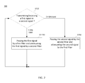
- FIG. 7 is a flowchart 700 of a method of sharing an antenna to transmit or receive signals having different frequencies according to an embodiment.
- a first signal having a first frequency in a 5 GHz frequency band and a second signal having a second frequency in a 2.4 GHZ frequency band are handled by a first transceiver for WiFiTM communication and a second transceiver for Bluetooth® communication, respectively.
- a first signal or a second signal is transmitted or received by the shared antenna.
- the method 700 proceeds to S 7 - 730 .
- the method 700 proceeds to S 750 .
- a first filter passes the first signal to transmit/receive the first signal to/from the first transceiver.
- a second filter attenuates the first signal to prevent the first signal being transmitted/received to/from the second transceiver.
- the second filter passes the second signal to transmit/receive the second signal to/from the second transceiver.
- the first filter attenuates the second signal to prevent the second signal being transmitted/received to/from the first transceiver.
- FIGS. 8A and 8B are flowcharts of a method 8 - 730 of operating a first filter and a second filter when a first signal having a first frequency is received/transmitted, according to an embodiment, such as may be used at S 7 - 730 of the method 700 shown in FIG. 7 .
- the first filter includes a parallel LC circuit having a capacitor and a first inductor, and a second inductor coupled to the parallel LC circuit in series.
- FIG. 8A is a flowchart 8 - 730 a of a method of passing a first signal having a first frequency by a first filter.
- the parallel LC circuit of the first filter presents a predominantly capacitive impedance.
- the first filter in this embodiment becomes substantially equivalent to a series LC circuit including the first capacitor and the second inductor.
- an impedance value of the series LC circuit at the first frequency is minimized.
- the first filter passes the first signal to or from the first transceiver circuit.
- a second filter is coupled to the antenna and a second transceiver circuit.
- the second filter includes a parallel LC circuit having a first capacitor and an inductor, and a second capacitor coupled to the parallel LC circuit in series.
- FIG. 8B is a flowchart 8 - 730 b of a method of attenuating the first signal having the first frequency by a second filter.
- the parallel LC circuit of the second filter has the maximum impedance value at the first frequency.
- the second filter in this embodiment substantially attenuates the first signal to prevent the first signal being transmitted/received to/from the second transceiver circuit.
Abstract
Description
In this embodiment, the first filter 3-120 a acting as the series LC circuit has the second resonant frequency f2 that is substantially equal to a frequency within the 5 GHz band.
In this embodiment, the second filter 3-140 a acting as the series LC circuit has the fourth resonant frequency f4 that is substantially equal to a frequency in the 2.4 GHz band.
Claims (20)
Priority Applications (1)
| Application Number | Priority Date | Filing Date | Title |
|---|---|---|---|
| US14/332,341 US9401798B1 (en) | 2013-07-15 | 2014-07-15 | Frequency domain multiplexer |
Applications Claiming Priority (2)
| Application Number | Priority Date | Filing Date | Title |
|---|---|---|---|
| US201361846575P | 2013-07-15 | 2013-07-15 | |
| US14/332,341 US9401798B1 (en) | 2013-07-15 | 2014-07-15 | Frequency domain multiplexer |
Publications (1)
| Publication Number | Publication Date |
|---|---|
| US9401798B1 true US9401798B1 (en) | 2016-07-26 |
Family
ID=56411136
Family Applications (1)
| Application Number | Title | Priority Date | Filing Date |
|---|---|---|---|
| US14/332,341 Expired - Fee Related US9401798B1 (en) | 2013-07-15 | 2014-07-15 | Frequency domain multiplexer |
Country Status (1)
| Country | Link |
|---|---|
| US (1) | US9401798B1 (en) |
Cited By (2)
| Publication number | Priority date | Publication date | Assignee | Title |
|---|---|---|---|---|
| CN109450496A (en) * | 2018-10-11 | 2019-03-08 | 展讯通信(上海)有限公司 | Antenna duplexer system, terminal |
| CN111726127A (en) * | 2019-03-18 | 2020-09-29 | 三星电机株式会社 | Front end module |
Citations (1)
| Publication number | Priority date | Publication date | Assignee | Title |
|---|---|---|---|---|
| US8081048B2 (en) * | 2008-08-27 | 2011-12-20 | Renesas Electronics Corporation | Branching filter, semiconductor integrated circuit device, and communication mobile terminal |
-
2014
- 2014-07-15 US US14/332,341 patent/US9401798B1/en not_active Expired - Fee Related
Patent Citations (1)
| Publication number | Priority date | Publication date | Assignee | Title |
|---|---|---|---|---|
| US8081048B2 (en) * | 2008-08-27 | 2011-12-20 | Renesas Electronics Corporation | Branching filter, semiconductor integrated circuit device, and communication mobile terminal |
Non-Patent Citations (3)
| Title |
|---|
| Gianesello et al, Integration of multi-standard Front End Modules SOCs on High Resitivity SOI RF CMOS Technogy, IEEE, 4 pages, 2010. * |
| Kim et al, A Novel Integrated Tx-Rx Diplexer for Dual-band WiMAX System, IEEE, 4 pages, 2010. * |
| Wu et al, Wi-Fi/WiMAX Dual Mode RF MMIC Front-end Module, IEEE, 4 pages, 2009. * |
Cited By (4)
| Publication number | Priority date | Publication date | Assignee | Title |
|---|---|---|---|---|
| CN109450496A (en) * | 2018-10-11 | 2019-03-08 | 展讯通信(上海)有限公司 | Antenna duplexer system, terminal |
| CN109450496B (en) * | 2018-10-11 | 2021-10-22 | 展讯通信(上海)有限公司 | Antenna sharing system and terminal |
| US11387869B2 (en) * | 2018-10-11 | 2022-07-12 | Spreadtrum Communications (Shanghai) Co., Ltd. | Antenna sharing system and terminal |
| CN111726127A (en) * | 2019-03-18 | 2020-09-29 | 三星电机株式会社 | Front end module |
Similar Documents
| Publication | Publication Date | Title |
|---|---|---|
| US11652462B2 (en) | Multiplexer with hybrid acoustic passive filter | |
| US10727805B2 (en) | Multiplexer including filters with resonators and parallel inductor | |
| US10148249B2 (en) | High frequency circuit and communication apparatus | |
| JP5237138B2 (en) | Filters, duplexers, communication modules | |
| US9203451B2 (en) | System and method for an RF receiver | |
| JP4979897B2 (en) | Elastic wave filter and elastic wave duplexer | |
| JP5177589B2 (en) | Duplexer and electronic equipment | |
| US8179207B2 (en) | Resonator device, filter including the same, and duplexer | |
| US9979379B2 (en) | Multiplexer, radio frequency front-end circuit, communication device, and multiplexer design method | |
| US20150295559A1 (en) | Multiplexer using multiple tuned output impedances for reduced harmonic generation | |
| US10651821B2 (en) | Multiplexer, high-frequency front-end circuit, and communication apparatus | |
| EP2870701B1 (en) | Transceiver front-end | |
| US10700659B2 (en) | Multiplexer, radio-frequency front end circuit, and communication terminal | |
| US20190149130A1 (en) | Ladder-type frequency-variable filter, multiplexer, radio-frequency front end circuit, and communication terminal | |
| US7262674B2 (en) | Bandpass filter having first and second serially coupled collection of filter components for providing upper and lower rejection notches | |
| US11621699B2 (en) | Acoustic wave filter device and composite filter device | |
| US9401798B1 (en) | Frequency domain multiplexer | |
| US9935612B2 (en) | Ladder-type filter, duplexer, and module | |
| JP2008085775A (en) | High frequency circuit and semiconductor device | |
| US9419582B2 (en) | Filter device and duplexer | |
| US9825606B2 (en) | Wireless communication device and filter thereof | |
| US10951196B2 (en) | Multiplexer, high-frequency front-end circuit, and communication device | |
| Hu et al. | Temperature compensated band-pass and band-stop bulk-acoustic-wave filters solution reducing interference in wireless systems | |
| JP5503764B2 (en) | Filters, duplexers, communication modules | |
| US9929759B1 (en) | Integrated duplexer |
Legal Events
| Date | Code | Title | Description |
|---|---|---|---|
| AS | Assignment |
Owner name: MARVELL INTERNATIONAL LTD., BERMUDA Free format text: ASSIGNMENT OF ASSIGNORS INTEREST;ASSIGNOR:MARVELL SEMICONDUCTOR, INC.;REEL/FRAME:038340/0342 Effective date: 20160421 Owner name: MARVELL SEMICONDUCTOR, INC., CALIFORNIA Free format text: ASSIGNMENT OF ASSIGNORS INTEREST;ASSIGNORS:SIGNOFF, DAVID M;WONG, ALDEN CHEE HO;MANIAM, NUNTHA KUMAR KRISHNASAMY;SIGNING DATES FROM 20140714 TO 20160420;REEL/FRAME:038340/0312 |
|
| STCF | Information on status: patent grant |
Free format text: PATENTED CASE |
|
| AS | Assignment |
Owner name: CAVIUM INTERNATIONAL, CAYMAN ISLANDS Free format text: ASSIGNMENT OF ASSIGNORS INTEREST;ASSIGNOR:MARVELL INTERNATIONAL LTD.;REEL/FRAME:052918/0001 Effective date: 20191231 |
|
| FEPP | Fee payment procedure |
Free format text: MAINTENANCE FEE REMINDER MAILED (ORIGINAL EVENT CODE: REM.); ENTITY STATUS OF PATENT OWNER: LARGE ENTITY |
|
| AS | Assignment |
Owner name: MARVELL ASIA PTE, LTD., SINGAPORE Free format text: ASSIGNMENT OF ASSIGNORS INTEREST;ASSIGNOR:CAVIUM INTERNATIONAL;REEL/FRAME:053475/0001 Effective date: 20191231 |
|
| LAPS | Lapse for failure to pay maintenance fees |
Free format text: PATENT EXPIRED FOR FAILURE TO PAY MAINTENANCE FEES (ORIGINAL EVENT CODE: EXP.); ENTITY STATUS OF PATENT OWNER: LARGE ENTITY |
|
| STCH | Information on status: patent discontinuation |
Free format text: PATENT EXPIRED DUE TO NONPAYMENT OF MAINTENANCE FEES UNDER 37 CFR 1.362 |
|
| FP | Lapsed due to failure to pay maintenance fee |
Effective date: 20200726 |