US9396155B2 - Envelope detection device and related communication device - Google Patents
Envelope detection device and related communication device Download PDFInfo
- Publication number
- US9396155B2 US9396155B2 US14/600,016 US201514600016A US9396155B2 US 9396155 B2 US9396155 B2 US 9396155B2 US 201514600016 A US201514600016 A US 201514600016A US 9396155 B2 US9396155 B2 US 9396155B2
- Authority
- US
- United States
- Prior art keywords
- reference signal
- transistor
- circuit
- state
- envelope detection
- Prior art date
- Legal status (The legal status is an assumption and is not a legal conclusion. Google has not performed a legal analysis and makes no representation as to the accuracy of the status listed.)
- Active
Links
Images


Classifications
-
- G—PHYSICS
- G06—COMPUTING OR CALCULATING; COUNTING
- G06F—ELECTRIC DIGITAL DATA PROCESSING
- G06F13/00—Interconnection of, or transfer of information or other signals between, memories, input/output devices or central processing units
- G06F13/38—Information transfer, e.g. on bus
- G06F13/42—Bus transfer protocol, e.g. handshake; Synchronisation
- G06F13/4282—Bus transfer protocol, e.g. handshake; Synchronisation on a serial bus, e.g. I2C bus, SPI bus
-
- G—PHYSICS
- G06—COMPUTING OR CALCULATING; COUNTING
- G06F—ELECTRIC DIGITAL DATA PROCESSING
- G06F13/00—Interconnection of, or transfer of information or other signals between, memories, input/output devices or central processing units
- G06F13/38—Information transfer, e.g. on bus
- G06F13/40—Bus structure
- G06F13/4063—Device-to-bus coupling
- G06F13/4068—Electrical coupling
- G06F13/4072—Drivers or receivers
-
- H—ELECTRICITY
- H04—ELECTRIC COMMUNICATION TECHNIQUE
- H04B—TRANSMISSION
- H04B17/00—Monitoring; Testing
-
- H—ELECTRICITY
- H04—ELECTRIC COMMUNICATION TECHNIQUE
- H04B—TRANSMISSION
- H04B1/00—Details of transmission systems, not covered by a single one of groups H04B3/00 - H04B13/00; Details of transmission systems not characterised by the medium used for transmission
- H04B1/69—Spread spectrum techniques
- H04B2001/6912—Spread spectrum techniques using chirp
Definitions
- the present invention relates generally to signal transmission, and more particularly, to an envelope detection device and communication device that detect transmission state and disconnect state of the signal transmission by sharing single comparison circuit.
- the communication device may detect signal levels on the buses by utilizing some envelope detectors. When signal levels are lower than certain thresholds, the communication device would recognize that no signals are currently on the buses. At this time, the communication device may enter specific states and may not process the signals received from the buses. Furthermore, the communication device may recognize that other remote communication device on the buses is disconnected if the signal level on the buses is, for example, higher than certain thresholds.
- the USB device may have to detect squelch state, Chirp J/K state (which is state related to handshake for switching from a reset period into a high-speed mode), and disconnect state that is related to connections between devices, depending on its operation mode (e.g. host mode or device).
- the receiver of the USB device may include multiple envelope detection devices (envelope detectors). These detectors are respectively responsible for comparing a potential difference between the signal lines D+ and D ⁇ of the USB bus (i.e., a USB differential signal) with multiple reference levels.
- the differential signal is smaller than or equal to 100 mV, it is recognized as at the squelch state; and if it is detected that the differential signal is greater than or equal to 150 mV, it must not be recognized as the squelch state.
- the differential signal is greater than or equal to 300 mV, it is recognized as at the Chirp J state.
- the differential signal is smaller than or equal to ⁇ 300 mV, it is recognized as at the Chirp K state.
- the differential signal is greater than or equal to 625 mV, it is recognized as at the disconnect state. When the differential signal is smaller than or equal to 525 mV, it must not be recognized as disconnect state.
- the receiver needs multiple envelope detection devices and each envelope detection device needs respective comparison circuit and reference signal generation circuit in order to compare the differential signal on the signal lines D+ and D ⁇ with the reference signal at different levels (e.g. 100 mV, 150 mV, ⁇ 300 mV, 525 mV and 625 mV).
- the quantity of comparison circuits and reference signal generation circuits directly leads to an increase in circuitry complexity and manufacturing costs of the receiver.
- the present invention provides an inventive architecture of the envelope detection device, where multiple envelope detection devices share single comparing circuit to detect different transmission states and disconnect state. Furthermore, the present invention further provides a communication device based on the inventive envelope detection device.
- the operation circuit is employed for receiving the transmission signal and generating a set of operation outputs according to the transmission signal and at least one reference signal.
- the reference signal generation circuit is coupled to the operation circuit, and employed for providing the reference signal to the operation circuit, wherein the reference signal generation circuit is operable to provide the reference signal with different levels.
- the comparison circuit is coupled to the operation circuit, and employed for comparing the set of the operation outputs to generate a comparison result.
- the envelope detection device detects a transmission state and a disconnect state of the high speed serial communication according to comparison results that are generated based on the reference signal at different levels.
- a communication device comprises a physical layer circuit and a medium access control layer circuit.
- the physical layer circuit comprises an envelope detection circuit for detecting a transmission signal of a high speed serial communication carried out by the communication device.
- the envelope detection device comprises: an operation circuit, a reference signal generation circuit and a comparison circuit.
- the operation circuit is employed for receiving the transmission signal and generating a set of operation outputs according to the transmission signal and at least one reference signal.
- the reference signal generation circuit is coupled to the operation circuit, and employed for providing the reference signal to the operation circuit, wherein the reference signal generation circuit is operable to provide the reference signal with different levels.
- the comparison circuit is coupled to the operation circuit, and employed for comparing the set of the operation outputs to generate a comparison result.
- the envelope detection device detects a transmission state and a disconnect state of the high speed serial communication according to comparison results that are generated based on the reference signal at different levels.
- the medium access control layer circuit is coupled to the physical layer circuit, and employed for providing an output state selection signal to the envelope detection device, allowing the envelope detection device to detect one of the transmission state and the disconnect state of the high speed serial communication, and the reference signal generation circuit determines a level of the reference signal according to the output state selection signal, and the envelope detection device generates a corresponding state indication signal, the medium access control layer circuit operates according to the state indication signal.
- the inventive envelope detection device provided by the present invention can detect multiple different states of the communication, the quantity of the envelope detection device required by a communication device is significantly reduced.
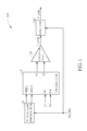
- FIG. 1 illustrates a block diagram of an envelope detection device according to one embodiment of the present invention.
- FIG. 2 illustrates a circuit diagram of a first embodiment of the operation circuit of the envelope detection device.
- FIG. 3 illustrates a circuit diagram of a second embodiment of the operation circuit of the envelope detection device.
- FIG. 4 illustrates a circuit diagram of an embodiment of the reference signal generation circuit of the envelope detection device.
- FIG. 5 illustrates a circuit diagram of a third embodiment of the operation circuit of the envelope detection device.
- FIG. 6 illustrates a circuit diagram of another embodiment of the reference signal generation circuit of the envelope detection device.
- FIG. 7 illustrates a block diagram of a communication device according to one embodiment of the present invention.
- FIG. 1 illustrates a block diagram of an envelope detection device according to one embodiment of the present invention.
- the envelope detection device 100 is intended for detecting a transmission signal of a high speed serial communication.
- the transmission signal is a differential signal, which consists of a set of complementary signals DP and DM.
- the envelope detection device 100 includes: an operation circuit 110 , a reference signal generation circuit 120 , and a comparison circuit 130 .
- the present embodiment relies on the operation circuit 110 and the reference signal generation circuit 120 to achieve the objective.
- the transmission signals DP and DM and various thresholds corresponding to different states, different operation outputs will be obtained and provided to the comparison circuit 130 for comparison such that comparison results corresponding to different states can be generated.
- the operation circuit 110 performs a calculation operation on the transmission signals DP and DM with the reference signal VREF 1 or with the reference signals VREF 1 and VREF 2 to generate a set of operation results including a signal V 1 and a signal V 2 for the comparison circuit 130 to compare.
- the comparison circuit 130 apparently compares the signal V 1 with the signal V 2 , the outcome is substantially equal to the result of compare (DP ⁇ DM) with (VREF 2 ⁇ VREF 1 ), or (DP ⁇ DM) with VREF 1 .
- the differential signal when the differential signal is greater than 150 mV, it must not be recognized as the squelch state, and when the differential signal is smaller than 100 mV, it is recognized as the squelch state.
- an average of 100 mV and 150 mV could be used as the determination threshold.
- the envelop detection device 100 is able to detect the squelch state.
- the reference signal generation circuit 120 could generate two sets of outputs respectively corresponding to 100 mV and 150 mV, and the comparison circuit 130 compares V 1 and V 2 for the determination threshold of 100 mV and the determination threshold of 150 mV, respectively.
- the comparison result V_comp of the comparison circuit 130 whether the USB communication enters the squelch state may thus be determined. For instance, when the comparison result V_comp indicates V 1 is smaller than V 2 , the USB communication is determined to enter the squelch state.
- the reference signal generation circuit 120 will have the reference signals VREF 1 and VREF 2 meet the condition that VREF 2 ⁇ VREF 1 is equal to 300 mV, or VREF 1 is equal to 300 mV (for Chirp J state); or VREF 2 ⁇ VREF 1 is equal to ⁇ 300 mV, or VREF 1 is equal to ⁇ 300 mV (for Chirp K state).
- the Chirp J/K state could be detected based on the comparison result V_comp of the comparison circuit 130 .
- any voltage between 525 mV and 625 mV can be used to generate the reference signal VREF 1 , or references signals VREF 1 and VREF 2 .
- the envelope detection device 100 is controlled by an output state selection signal ED_SEL.
- the output state selection signal ED_SEL may be used to select one of the above mentioned states of the USB communication the envelope detection device 100 should detect, and the reference signal generation circuit 120 accordingly generates corresponding reference signals VREF 1 and VREF 2 .
- the operation circuit 110 includes two differential pairs, one of which is comprised of transistors Q 1 and Q 2 , while the other of which is comprised of transistors Q 3 and Q 4 .
- the differential pair comprised of transistors Q 1 and Q 2 is biased by a current source I o
- the differential pair comprised of transistors Q 3 and Q 4 is biased by a current source I o ′. Currents flowing through each transistor are designated as shown in figure. Control ends G 1 and G 2 (e.g.
- the comparison circuit 130 compares the operation output V 1 with the operation output V 2 , and could derive the comparison result of V 1 >V 2 , or the comparison result of V 1 ⁇ V 2 . Hence, when the comparison circuit 130 detects V 1 >V 2 , it represents V 1 ⁇ V 2 >0 and thus (DP ⁇ DM) is greater than (VREF 2 ⁇ VREF 1 ). When the comparison circuit 130 detects V 1 ⁇ V 2 , it thus represents (DP ⁇ DM) is smaller than (VREF 2 ⁇ VREF 1 ). As long as levels of the reference signals VREF 1 and VREF 2 that are generated by the reference signal generation circuit 120 can be properly set, the comparison circuit 130 can correctly recognize different states.
- FIG. 3 illustrates a second embodiment of the operation circuit 110 .
- This embodiment is generally similar to the first embodiment in configuration, and repeated descriptions are omitted here.
- the difference between the second embodiment and the first embodiment is that the control end G 3 of the transistor Q 3 is coupled to a ground and the control end G 4 of the transistor Q 4 is coupled to the reference signal VREF 1 in the second embodiment.
- V 1 ⁇ V 2 Ro*K [( DP ⁇ DM ) ⁇ V REF1];
- the comparison circuit 130 detects V 1 >V 2 , (DP ⁇ DM) is greater than VREF 1 ; otherwise, (DP ⁇ DM) is smaller than VREF 1 .
- the reference signal generation circuit 120 even though the reference signal generation circuit 120 only generates the reference signal VREF 1 instead of both VREF 1 and VREF 2 , this embodiment still achieves the same result as the first embodiment which generates a set of reference signals.
- the reference signal generation circuit 120 can be implemented with the architecture shown on the right side of FIG. 3 , where the reference signal generation circuit 120 includes a constant current source 124 and a resistor network 126 .
- the reference signal generation circuit 120 may selectively change connection between its output terminal (labeled with VREF 1 ) and nodes E 1 or E 2 of the resistor network 126 .
- the reference signal VREF 1 with higher level could be obtained.
- the reference signal VREF 1 with lower level could be obtained.
- the resistor network 126 includes more resistive elements (eg. resistors) and nodes, various and different voltage levels of the reference signal VREF 1 can be obtained.
- the reference signal generation circuit 120 could be also implemented by a single resistive element and an adjustable current source as shown by FIG. 4 . Specifically, different levels of the reference signal VREF 1 can be obtained by varying an output current of the adjustable current source I VAR .
- FIG. 5 illustrates a third embodiment of the operation circuit 110 of the present invention.
- the operation circuit 110 includes a differential pair that is comprised of transistors Q 1 and Q 2 . Gates G 1 of the transistor Q 1 and G 2 of the transistor Q 2 are respectively coupled to the transmission signals DP and DM. Assuming that the voltage difference across the gate G 1 and the drain D 1 of the transistor Q 1 and the voltage difference across the gate G 2 and the drain D 2 of the transistor Q 2 are both VG (because the transistors Q 1 and Q 2 consist of a differential pair, voltage differences across their corresponding nodes would be identical), the voltage level on the drain D 1 of the transistor Q 1 and the voltage level on the drain D 2 of the transistor Q 2 is (DP+VG) and (DM+VG), respectively.
- different comparison results of the comparison circuit 130 can reflect either (DP ⁇ DM) is greater than (VREF 2 ⁇ VREF 1 ) or (DP ⁇ DM) is smaller than (VREF 2 ⁇ VREF 1 ).
- the controlled voltage source ⁇ VREF can be implemented with the reference signal generation circuit 120 as shown by FIG. 6 , wherein output terminals corresponding to reference signals VREF 2 and VREF 1 could respectively serve as nodes X 1 and X 2 of the voltage source ⁇ VREF.
- the output state selection signal ED_SEL could be used to select connection between the output terminal and the node E 3 or between the output terminal and node E 4 of the resistor network, which leads to different values of (VREF 2 ⁇ VREF 1 ).
- the controlled voltage source ⁇ VREF could be implemented with architecture shown in FIG. 4 , including an adjustable current source and a resistive element, which uses two ends of the resistive element as output terminals E 3 and E 4 of the voltage source ⁇ VREF.
- the comparison result V_comp generated by the comparison circuit 130 can recognize a specific transmission state or a specific connection state
- the comparison result V_comp could be further processed by a logic circuit 140 before it serves as a state indication.
- the logic circuit 140 could include a filter circuit, a de-glitch circuit, and/or a delay circuit.
- the logic circuit 140 could perform further processing on the comparison result V_comp generated by the comparison circuit 130 to generate a state indication signal V_cond such that misjudgments on states can be prevented and detection accuracy can be improved.
- the logic circuit 140 could be omitted in some embodiments.
- the envelope detection device 100 may directly use the comparison result V_comp generated by the comparison circuit 130 to indicate states of the USB communication.
- the inventive envelope detection device 100 will not cause resource contention even if the different states are detected by a same comparison circuit.
- a communication device 200 includes a physical (PHY) layer circuit 210 and a medium access control (MAC) layer circuit.
- the PHY layer circuit 210 includes a USB transceiver, which is used for receiving/transmitting the transmission signals DP and DM from/to the USB bus, encoding/decoding, modulating/demodulating the transmission signal.
- the PHY layer circuit 210 also includes the envelope detection device 100 of FIG. 1 , for detecting the transmission state and the disconnect state of the USB communication.
- the transmission state includes at least one of the squelch state and the Chirp J/K state.
- the MAC layer circuit 220 issues the output state selection signal ED_SEL to the PHY layer circuit 210 to determine which state the envelope detection device 100 should detect, and instructs the envelope detection device 100 to generate the state indication signal V_comp for indicating the detected state. Furthermore, after the envelope detection device 100 receives the output state selection signal ED_SEL, the reference signal generation circuit 120 also generates corresponding reference signal, allowing the comparison circuit 130 to generate the comparison result, thus indicating the transmission state and the disconnect state. As a result, the MAC layer circuit 220 performs corresponding operations according to the state indication signal V_comp.
- the inventive envelope detection device is also feasible to any types of data transmission interface. As long as a data transmission interface needs to detect multiple transmission states and disconnect state (having different determination thresholds), and uses differential signaling, the inventive envelope detection device can be applied to such data transmission interface to simplify the circuitry complexity.
Landscapes
- Engineering & Computer Science (AREA)
- Theoretical Computer Science (AREA)
- General Engineering & Computer Science (AREA)
- Physics & Mathematics (AREA)
- General Physics & Mathematics (AREA)
- Computer Hardware Design (AREA)
- Electromagnetism (AREA)
- Computer Networks & Wireless Communication (AREA)
- Signal Processing (AREA)
- Dc Digital Transmission (AREA)
Abstract
Description
V1−V2=K[(DP−DM)−(VREF2−VREF1)]; or
V1−V2=K[(DP−DM)−(VREF1)];
I1−I2=K1*(DP−DM);
-
- where K1 is the differential transconductance of the transistors Q1 and Q2; and the difference between current I3 and I4 could be represented as:
I3−I4=K2*(VREF1−VREF2);
where K2 is the differential transconductance of the transistors Q3 and Q4.
- where K1 is the differential transconductance of the transistors Q1 and Q2; and the difference between current I3 and I4 could be represented as:
(I1+I3)−(I2+I4)=K(DP−DM)+K(VREF1−VREF2).
Ro[(I1+I3)−(I2+I4)]=Ro*K[(DP−DM)+(VREF1−VREF2)].
V1−V2=Ro*K[(DP−DM)−(VREF2−VREF1)].
V1−V2=Ro*K[(DP−DM)−VREF1];
V1−V2=(DP−DM)−(VREF2−VREF1)
Claims (17)
Applications Claiming Priority (3)
| Application Number | Priority Date | Filing Date | Title |
|---|---|---|---|
| CN201410527287.3A CN105577580B (en) | 2014-10-09 | 2014-10-09 | Envelope detection apparatus and related communication apparatus |
| CN201410527287 | 2014-10-09 | ||
| CN201410527287.3 | 2014-10-09 |
Publications (2)
| Publication Number | Publication Date |
|---|---|
| US20160103781A1 US20160103781A1 (en) | 2016-04-14 |
| US9396155B2 true US9396155B2 (en) | 2016-07-19 |
Family
ID=55655546
Family Applications (1)
| Application Number | Title | Priority Date | Filing Date |
|---|---|---|---|
| US14/600,016 Active US9396155B2 (en) | 2014-10-09 | 2015-01-20 | Envelope detection device and related communication device |
Country Status (2)
| Country | Link |
|---|---|
| US (1) | US9396155B2 (en) |
| CN (1) | CN105577580B (en) |
Cited By (1)
| Publication number | Priority date | Publication date | Assignee | Title |
|---|---|---|---|---|
| US20220329207A1 (en) * | 2021-03-30 | 2022-10-13 | Stmicroelectronics S.R.L. | Envelope detector circuit, corresponding receiver circuit and galvanic isolator device |
Families Citing this family (6)
| Publication number | Priority date | Publication date | Assignee | Title |
|---|---|---|---|---|
| US9696351B2 (en) * | 2014-12-30 | 2017-07-04 | Stmicroelectronics International N.V. | Data receiving device including an envelope detector and related methods |
| US10120436B2 (en) * | 2016-03-23 | 2018-11-06 | Intel Corporation | Apparatuses, systems, and methods for USB high-speed chirp detection |
| US10908671B2 (en) | 2016-09-30 | 2021-02-02 | Maxim Integrated Products, Inc. | Method and apparatus for disabling high speed bus operation under high common mode voltage conditions |
| CN106533631B (en) * | 2016-12-15 | 2019-10-25 | 中国科学院深圳先进技术研究院 | Multi-antenna decoding circuit |
| US11029750B2 (en) * | 2017-06-29 | 2021-06-08 | Intel Corporation | Apparatus for universal serial bus 2.0 (USB2) combined high speed squelch and disconnect detection |
| CN109813952A (en) * | 2018-12-12 | 2019-05-28 | 珠海亿智电子科技有限公司 | A kind of envelope detected circuit |
Citations (2)
| Publication number | Priority date | Publication date | Assignee | Title |
|---|---|---|---|---|
| US20070118674A1 (en) * | 2005-11-18 | 2007-05-24 | Jonas Ulenas | Method and apparatus for enhancing universal serial bus |
| US20140207984A1 (en) * | 2013-01-24 | 2014-07-24 | Texas Instruments Incorporated | Signal conitioner |
Family Cites Families (3)
| Publication number | Priority date | Publication date | Assignee | Title |
|---|---|---|---|---|
| KR100375234B1 (en) * | 2001-03-30 | 2003-03-08 | 삼성전자주식회사 | Squelch detection circuit |
| CN102832956B (en) * | 2011-06-16 | 2016-01-20 | 晨星软件研发(深圳)有限公司 | Envelope detector and correlation technique |
| KR20140055580A (en) * | 2012-10-31 | 2014-05-09 | 엘에스산전 주식회사 | Demodulator and method of operation thereof |
-
2014
- 2014-10-09 CN CN201410527287.3A patent/CN105577580B/en active Active
-
2015
- 2015-01-20 US US14/600,016 patent/US9396155B2/en active Active
Patent Citations (2)
| Publication number | Priority date | Publication date | Assignee | Title |
|---|---|---|---|---|
| US20070118674A1 (en) * | 2005-11-18 | 2007-05-24 | Jonas Ulenas | Method and apparatus for enhancing universal serial bus |
| US20140207984A1 (en) * | 2013-01-24 | 2014-07-24 | Texas Instruments Incorporated | Signal conitioner |
Cited By (2)
| Publication number | Priority date | Publication date | Assignee | Title |
|---|---|---|---|---|
| US20220329207A1 (en) * | 2021-03-30 | 2022-10-13 | Stmicroelectronics S.R.L. | Envelope detector circuit, corresponding receiver circuit and galvanic isolator device |
| US12095423B2 (en) * | 2021-03-30 | 2024-09-17 | Stmicroelectronics S.R.L. | Envelope detector circuit, corresponding receiver circuit and galvanic isolator device |
Also Published As
| Publication number | Publication date |
|---|---|
| US20160103781A1 (en) | 2016-04-14 |
| CN105577580A (en) | 2016-05-11 |
| CN105577580B (en) | 2019-01-08 |
Similar Documents
| Publication | Publication Date | Title |
|---|---|---|
| US9396155B2 (en) | Envelope detection device and related communication device | |
| US7557633B2 (en) | High speed analog envelope detector | |
| EP2996247B1 (en) | Demodulation of on-off-key modulated signals in signal isolator systems | |
| EP3734414B1 (en) | Signal detector | |
| US10536309B2 (en) | Demodulation of on-off-key modulated signals in signal isolator systems | |
| US9483435B2 (en) | USB transceiver | |
| US7831223B2 (en) | Automatic adjustment circuit for amplitude of differential signal | |
| JP4818928B2 (en) | Method and apparatus for receiver detection on a PCI Express bus | |
| US20080100347A1 (en) | Signal detecting circuit | |
| US6486710B1 (en) | Differential voltage magnitude comparator | |
| US7589559B2 (en) | Current mode circuitry to modulate a common mode voltage | |
| US10432188B2 (en) | Ringing suppression circuit and ringing suppression method | |
| US20180074125A1 (en) | Circuit and Method for Differential Signal Skew Detection | |
| US20040000633A1 (en) | Optical receiver circuit, method, and system | |
| EP1145426B1 (en) | Data pulse receiver | |
| CN104375547B (en) | The system of sense terminals load | |
| US11575370B2 (en) | Power transistor detection with self-protection | |
| US6108528A (en) | Receive squelch circuit having function of detecting pulse width | |
| US6326817B1 (en) | Circuit for suppressing a common mode component in a signal from a CAN communication bus | |
| US9712344B2 (en) | Receiving device with error detection circuit | |
| US7474133B1 (en) | Apparatus and method for high-speed serial communications | |
| US7477077B1 (en) | Apparatus and method for loss of signal detection in a receiver | |
| CN204347831U (en) | Unidirectional RS-422 data communication system and receiving terminal | |
| US7279975B2 (en) | Differential circuit with offset control | |
| EP3157219B1 (en) | Demodulation of on-off modulated signals in signal isolator systems |
Legal Events
| Date | Code | Title | Description |
|---|---|---|---|
| AS | Assignment |
Owner name: ALI CORPORATION, TAIWAN Free format text: ASSIGNMENT OF ASSIGNORS INTEREST;ASSIGNORS:LIN, KUO-KAI;KAO, WEI-CHUN;CHENG, CHING-CHUNG;REEL/FRAME:034748/0067 Effective date: 20141209 |
|
| STCF | Information on status: patent grant |
Free format text: PATENTED CASE |
|
| MAFP | Maintenance fee payment |
Free format text: PAYMENT OF MAINTENANCE FEE, 4TH YEAR, LARGE ENTITY (ORIGINAL EVENT CODE: M1551); ENTITY STATUS OF PATENT OWNER: LARGE ENTITY Year of fee payment: 4 |
|
| MAFP | Maintenance fee payment |
Free format text: PAYMENT OF MAINTENANCE FEE, 8TH YEAR, LARGE ENTITY (ORIGINAL EVENT CODE: M1552); ENTITY STATUS OF PATENT OWNER: LARGE ENTITY Year of fee payment: 8 |