US9312473B2 - Vertical hall effect sensor - Google Patents
Vertical hall effect sensor Download PDFInfo
- Publication number
- US9312473B2 US9312473B2 US14/041,063 US201314041063A US9312473B2 US 9312473 B2 US9312473 B2 US 9312473B2 US 201314041063 A US201314041063 A US 201314041063A US 9312473 B2 US9312473 B2 US 9312473B2
- Authority
- US
- United States
- Prior art keywords
- semiconductor
- hall effect
- electrode
- fingers
- semiconductor wafer
- Prior art date
- Legal status (The legal status is an assumption and is not a legal conclusion. Google has not performed a legal analysis and makes no representation as to the accuracy of the status listed.)
- Active
Links
- 230000005355 Hall effect Effects 0.000 title claims abstract description 69
- 239000004065 semiconductor Substances 0.000 claims abstract description 124
- 239000002800 charge carrier Substances 0.000 claims description 13
- 229910052710 silicon Inorganic materials 0.000 claims description 6
- 239000010703 silicon Substances 0.000 claims description 6
- 235000012431 wafers Nutrition 0.000 description 62
- 239000007943 implant Substances 0.000 description 16
- 239000002019 doping agent Substances 0.000 description 10
- 239000000463 material Substances 0.000 description 10
- 238000002955 isolation Methods 0.000 description 8
- XUIMIQQOPSSXEZ-UHFFFAOYSA-N Silicon Chemical compound [Si] XUIMIQQOPSSXEZ-UHFFFAOYSA-N 0.000 description 5
- 230000004048 modification Effects 0.000 description 4
- 238000012986 modification Methods 0.000 description 4
- 239000000758 substrate Substances 0.000 description 4
- 230000000694 effects Effects 0.000 description 2
- BHEPBYXIRTUNPN-UHFFFAOYSA-N hydridophosphorus(.) (triplet) Chemical compound [PH] BHEPBYXIRTUNPN-UHFFFAOYSA-N 0.000 description 2
- 238000004519 manufacturing process Methods 0.000 description 2
- 238000005259 measurement Methods 0.000 description 2
- 239000002245 particle Substances 0.000 description 2
- 230000009286 beneficial effect Effects 0.000 description 1
- 230000003247 decreasing effect Effects 0.000 description 1
- 238000010586 diagram Methods 0.000 description 1
- 238000005516 engineering process Methods 0.000 description 1
- 239000012212 insulator Substances 0.000 description 1
- 238000000034 method Methods 0.000 description 1
Images


Classifications
-
- H—ELECTRICITY
- H10—SEMICONDUCTOR DEVICES; ELECTRIC SOLID-STATE DEVICES NOT OTHERWISE PROVIDED FOR
- H10N—ELECTRIC SOLID-STATE DEVICES NOT OTHERWISE PROVIDED FOR
- H10N52/00—Hall-effect devices
- H10N52/101—Semiconductor Hall-effect devices
-
- H01L43/065—
-
- G—PHYSICS
- G01—MEASURING; TESTING
- G01R—MEASURING ELECTRIC VARIABLES; MEASURING MAGNETIC VARIABLES
- G01R33/00—Arrangements or instruments for measuring magnetic variables
- G01R33/02—Measuring direction or magnitude of magnetic fields or magnetic flux
- G01R33/06—Measuring direction or magnitude of magnetic fields or magnetic flux using galvano-magnetic devices
- G01R33/07—Hall effect devices
- G01R33/077—Vertical Hall-effect devices
-
- H01L27/22—
-
- H01L43/14—
-
- H—ELECTRICITY
- H10—SEMICONDUCTOR DEVICES; ELECTRIC SOLID-STATE DEVICES NOT OTHERWISE PROVIDED FOR
- H10B—ELECTRONIC MEMORY DEVICES
- H10B61/00—Magnetic memory devices, e.g. magnetoresistive RAM [MRAM] devices
-
- H—ELECTRICITY
- H10—SEMICONDUCTOR DEVICES; ELECTRIC SOLID-STATE DEVICES NOT OTHERWISE PROVIDED FOR
- H10N—ELECTRIC SOLID-STATE DEVICES NOT OTHERWISE PROVIDED FOR
- H10N52/00—Hall-effect devices
- H10N52/01—Manufacture or treatment
-
- H—ELECTRICITY
- H10—SEMICONDUCTOR DEVICES; ELECTRIC SOLID-STATE DEVICES NOT OTHERWISE PROVIDED FOR
- H10N—ELECTRIC SOLID-STATE DEVICES NOT OTHERWISE PROVIDED FOR
- H10N52/00—Hall-effect devices
- H10N52/80—Constructional details
-
- H—ELECTRICITY
- H10—SEMICONDUCTOR DEVICES; ELECTRIC SOLID-STATE DEVICES NOT OTHERWISE PROVIDED FOR
- H10N—ELECTRIC SOLID-STATE DEVICES NOT OTHERWISE PROVIDED FOR
- H10N59/00—Integrated devices, or assemblies of multiple devices, comprising at least one galvanomagnetic or Hall-effect element covered by groups H10N50/00 - H10N52/00
Definitions
- the Hall effect is a phenomenon whereby moving charged particles are deflected by a magnetic field within a charge carrier. This phenomenon has been put to practical use in Hall effect sensors utilizing a current through a semiconductor.
- the preferable current path in the semiconductor is modified by magnetic fields through the wafer. By detecting the preferred current path, the direction and magnetic field through the semiconductor wafer may be determined.
- Hall effect sensors use silicon wafers doped to create N-type or P-type semiconductors. Vertical Hall effect sensors are so called because they are used to measure magnetic fields in the plane of the wafer. In practice, many vertical Hall effect detectors employ multiple Hall effect sensors on a single semiconductor substrate, in order to more accurately detect the direction and magnitude of a magnetic field passing through the substrate.
- a vertical Hall effect sensor in one aspect, includes a semiconductor wafer having a first conductivity type and a plurality of semiconductive electrodes disposed on the semiconductor wafer.
- the plurality of semiconductive electrodes have the first conductivity type and include a source electrode, a first sensing electrode and a second sensing electrode, arranged such that the source electrode is between the first sensing electrode and the sensing electrode and a first drain electrode and a second drain electrode, arranged such that the first sensing electrode, second sensing electrode, and source electrode are between the first drain electrode and the second drain electrode.
- the vertical Hall effect sensor also includes a plurality of semiconductor fingers disposed on the semiconductor wafer and interdigitated with the plurality of semiconductive electrodes, the semiconductor fingers having a second conductivity type.
- a magnetic field sensing device in another aspect, includes as plurality of vertical Hall effect sensors interdigitated between electrodes of the Hall effect sensor.
- Each vertical Hall effect sensor includes electrically floating semiconductor fingers and the plurality of vertical Hall effect sensors are arranged in a toroid within a semiconductor wafer.
- a method of making a vertical Hall effect sensor includes forming an epitaxial layer of a semiconductor with a first conductivity type on a semiconductor substrate with a second conductivity type, selectively doping at least five electrodes with the first conductivity type on a surface of the epitaxial layer, selectively doping at least four semiconductor fingers that are interdigitated with the at least five electrodes, the at least four semiconductor fingers having the second conductivity type and selectively doping at least one blanket region with the first conductivity type within the epitaxial layer.
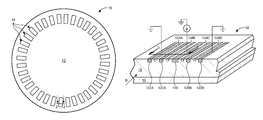
- FIG. 1 is a top view of a magnetic field sensing device utilizing vertical Hall effect sensors.
- FIG. 2 is a perspective cut-away view of a vertical Hall effect sensor along line 2 - 2 .
- FIG. 3 is a cross-sectional view of a portion of a vertical Hall effect sensor along line 3 - 3 .
- FIGS. 4A-4C are charts depicting equipotential lines in vertical Hall effect sensors.
- FIG. 5 is a chart depicting linearity of signal output of vertical Hall effect sensors.
- Described herein are techniques to detect magnetic fields in the plane of a semiconductor wafer. Due to advances in semiconductor technology, very small devices are capable of being made relatively quickly and easily. The underlying physics of the Hall effect is understood, but creating high output and linearity of that output remains a technological challenge.
- FIG. 1 is a top view of Hall sensor device 10 .
- Hall sensor device 10 includes semiconductor wafer 12 and vertical Hall effect sensors 14 .
- Hall sensor device 10 is a device capable of sensing magnetic fields.
- Hall sensor device 10 is capable of sensing magnetic fields in any direction in the plane including vertical Hall effect sensors 14 .
- Semiconductor wafer 12 is a piece of semiconducting material, for example a wafer cut from a silicon boule.
- Semiconductor wafer 12 may be doped to be N-type or P-type, for example by using a phosphorous dopant to add charge carriers to a silicon wafer.
- Semiconductor wafer 12 may vary widely in size depending on the intended use of Hall sensor device 10 .
- Typical sizes for vertical Hall sensors may be in the millimeter to micrometer range.
- the thickness of semiconductor wafer 12 affects maximum possible depth of current flow, and is often in the micrometer range. For example, it is very typical for a semiconductor wafer to be about 600 microns thick. However, only the top, epitaxial portion is important for the Hall sensor. This epitaxial portion is in the micrometer range, and could be as thin as perhaps 0.3 microns or as thick as perhaps 200 microns. In one particular example, the thickness of the epitaxial portion is about 7 microns.
- Semiconductor wafer 12 may be formed in alternative geometries.
- semiconductor wafer 12 as shown in FIG. 1 is a right cylinder, alternative geometries for semiconductor wafer 12 may include rectangular prisms or parallelograms.
- Semiconductor wafer 12 has an epitaxial portion, which includes all of semiconductor wafer 12 that is not doped as an electrode ( FIGS. 2-3 : 118 , 120 A- 120 B, 122 A- 122 B), an implant layer ( FIG. 3, 228 ), or a semiconductor finger ( FIG. 2, 124A-124D ). Doping levels within the epitaxial portion of semiconductor wafer 12 may be modified in order to facilitate desired current flow.
- retrograde dopant profiles may be used, in which the dopant level of semiconductor wafer 12 is increased or decreased with depth beneath the surface of semiconductor wafer 12 on which vertical Hall effect sensors 14 are arranged.
- This retrograde dopant profile may be beneficial in that it may be used to increase or decrease the depth at which current flows through semiconductor wafer 12 .
- Preferred paths for electrons flowing within semiconductor wafer 12 may be created by selectively doping regions of semiconductor wafer 12 with higher and lower levels of dopant, which modifies the charge carrier density therein. Modification of the charge carrier density affects resistivity of semiconductor materials.
- vertical Hall effect sensors 14 are modified vertical Hall effect sensors vertical Hall effect detectors.
- vertical Hall effect sensors 14 are typically made of a semiconductor material with various doping levels in different regions based on desired characteristics of Hall sensor device 10 .
- Hall sensor device 10 as shown in FIG. 1 , there are thirty-six vertical Hall effect sensors 14 .
- there may be more or fewer vertical Hall effect sensors 14 depending on the desired output from Hall sensor device 10 .
- alternative Hall sensor devices may only require one Hall feature, or may utilize several thousand vertical Hall effect sensors, or any number in between.
- vertical Hall effect sensors 14 are modified in order to increase the linearity and/or magnitude of the electrical signal produced in response to a magnetic field.
- Hall sensor device 10 is made up of semiconductor wafer 12 with vertical Hall effect sensors 14 built into at least one of its surfaces. Electrodes (shown in FIG. 2 ) may be connected in such a way that the output from each of vertical Hall effect sensors 14 may be measured, and the direction and strength of a magnetic field through Hall sensor device 10 may be determined.
- Semiconductor wafer 12 may be any wafer of semiconductive material, for example silicon. Often, the wafer is grown epitaxially, to facilitate the fabrication of regions with different doping levels.
- vertical Hall effect sensors 14 may be electrically connected to a meter (not shown) for data output, and in alternative embodiments may be either electrically connected to one another or electrically insulated from one another.
- Hall sensor device 10 can be used to measure the strength and direction of magnetic fields within the plane containing vertical Hall effect sensors 14 .
- Each Vertical Hall effect sensor 14 can measure the strength of the magnetic field in one direction. In the embodiment shown in FIG. 1 , each Vertical Hall effect sensor 14 is arranged such that it can measure the field in a direction radially inward or outward from the center of semiconductor wafer 12 .
- vertical Hall effect sensors 14 measure the strength of the magnetic field using Hall effect physics; thus, as the direction of the magnetic field being measured becomes perpendicular to the radially inner face of any Vertical Hall effect sensor 14 , the difference between the outputs from that Hall vertical Hall effect sensor 14 will increase. Conversely, as the direction of the magnetic field being measured becomes parallel to the radially inner face of any Hall vertical Hall effect sensor 14 , the difference between the outputs from that Hall vertical Hall effect sensor 14 will decrease.
- Hall sensor device 10 An important aspect of Hall sensor device 10 is the modification of vertical Hall effect sensors 14 .
- the modifications to vertical Hall effect sensors 14 as will be described with respect to FIGS. 2 and 3 , allow for greater accuracy of Hall sensor device 10 .
- FIG. 2 is a cross-sectional view of vertical Hall effect sensor 14 taken along line 2 - 2 of FIG. 1 .
- FIG. 2 shows semiconductor wafer 12 and isolation layer 16 , as well as vertical Hall effect sensor 14 .
- vertical Hall effect sensor 14 includes source electrode 118 , sense electrodes 120 A and 120 B, and drain electrodes 122 A and 122 B.
- vertical Hall effect sensor 14 further includes p-fingers 124 A, 124 B, 124 C, and 124 D.
- Semiconductor wafer 12 is any semiconductor layer, such as an N-type phosphorous doped silicon wafer.
- Isolation layer 16 is a layer of material which can prevent electrical current from flowing from source electrode 118 out of semiconductor wafer 12 .
- isolation layer 16 may be an insulator or a P-type semiconductor.
- Source electrode 118 , sense electrodes 120 A and 120 B, and drain electrodes 122 A and 122 B are electrodes used for measuring magnetic field through vertical Hall effect sensor 14 .
- These electrodes may be, for example, relatively heavily doped N-type semiconductor materials as compared to the dopant level in the epitaxial portion of semiconductor wafer 12 .
- P-fingers 124 A- 124 D in contrast, are P-type regions arranged between sense, drain, and source electrodes. While FIG.
- the dopant type may be reversed; that is, the p-fingers could be made of N-type semiconductor material and the epitaxial portion of semiconductor wafer 12 as well as source electrode 118 , sense electrodes 120 A- 120 B, and drain electrodes 122 A- 122 B may be P-type.
- the epitaxial semiconductor and electrodes are referred to as N-type, and the isolation layer and p-fingers are referred to as P-type.
- isolation layer 16 forms a substrate upon which semiconductor wafer 12 is arranged.
- Source electrode 118 which as shown in FIG. 2 is a bar-shaped electrode which is positively biased from ground.
- source electrode may be held at a specific voltage greater than the voltage at drain electrodes 122 A- 122 B.
- Sense electrodes 120 A and 120 B are disposed along the same surface of semiconductor wafer 12 , and are also bar shaped electrodes. Sense electrodes 120 A and 120 B are arranged on opposite sides of source electrode 118 .
- Sense electrodes 120 A and 120 B are electrically connected to a meter that determines the extent to which current preferentially flows to each of sense electrodes 120 A and 120 B.
- P-finger 124 B is arranged between source electrode 118 and sense electrode 120 A
- p-finger 124 C is arranged between source electrode 118 and sense electrode 120 B.
- Each of p-fingers 124 B and 124 C are bar-shaped regions of P-type semiconductor.
- Drain electrodes 122 A and 122 B are also N-type bar-shaped electrodes disposed along the same surface of semiconductor wafer 12 as source electrode 118 , sense electrodes 120 A- 120 B, and p-fingers 124 B- 124 C.
- Drain electrode 122 A is arranged opposite sense electrode 120 A from source electrode 118
- drain electrode 122 B is arranged opposite sense electrode 120 B from source electrode 118
- P-finger 124 A is arranged between drain electrode 122 A and sense electrode 120 A
- p-finger 124 D is arranged between drain electrode 122 B and sense electrode 120 B.
- Drain electrodes 122 A- 122 B are connected to ground.
- drain electrodes 122 A- 122 B and source electrode 118 may be kept at a constant voltage, so long as there is a voltage difference between source electrode 118 and drain electrodes 122 A- 122 B.
- An example of a magnetic field is also shown as magnetic field B.
- Vertical Hall effect sensor 14 as shown in FIG. 2 utilizes Hall effect physics to measure magnetic field.
- magnetic fields within semiconductor wafer 12 cause current to flow preferentially to either drain electrode 122 A or 122 B.
- a magnetic field in the opposite direction of magnetic field B would cause negative charge carriers to preferentially drift toward drain electrode 122 A, and a magnetic field perpendicular to B would cause no preferential drift, so the voltage at sense electrode 120 A would be roughly equivalent to the voltage at sense electrode 120 B.
- the deeper the current flows through semiconductor wafer 12 the greater the Hall effect on the moving charges, and the greater preferential drift towards either drain electrode 122 A or drain electrode 122 B.
- This preferential drift causes the voltage at sense electrodes 120 A- 120 B to vary depending on magnetic field.
- P-fingers 124 A- 124 D create depletion regions ( FIG. 3, 226 ) between source electrode 118 , sense electrodes 120 A- 120 B, and drain electrodes 122 A- 122 B.
- p-fingers 124 A- 124 D are floated, as opposed to grounded. This makes the depletion region surrounding p-fingers 124 A- 124 D smaller than in a configuration having grounded p-fingers. As a result, greater linearity of the output with respect to increased magnetic field is achieved. Further, P-fingers 124 A- 124 D are narrower than the P-type regions used previously in vertical Hall devices.
- P-fingers 124 A- 124 D may be, for example, between 0.5 micrometers and 1.2 micrometers in width, or more particularly between 0.6 micrometers and 0.8 micrometers in width, or even more particularly between 0.6 and 0.7 micrometers in width, for a semiconductor wafer that is 10 micrometers thick. Both of these changes—narrowing P-fingers 124 A- 124 D and floating them as opposed to grounding them—result in increased linearity of the output from vertical Hall effect sensor 14 . Both of these changes would, without further modifications to vertical Hall effect sensor 14 , result in shallower current flow depth, which, as previously described, would result in less signal output with greater linearity.
- FIG. 3 is a cross-sectional view of vertical Hall effect sensor 14 taken along line 3 - 3 of FIG. 2 .
- FIG. 3 shows source electrode 118 , sense electrode 120 A, and drain electrode 122 A.
- p-fingers 124 A and 124 B are interdigitated between source electrode 219 , sense electrode 120 A, and drain electrode 122 A. All of the electrodes and p-fingers are arranged within semiconductor wafer 12 , which is arranged epitaxially on top of isolation layer 16 .
- FIG. 3 shows depletion region 226 and N-type blankets 228 .
- N-type blankets 228 are regions with higher levels of N-type dopant than the surrounding epitaxial layers of semiconductor material 12 . As such, N-type blankets 228 have higher charge carrier density and lower resistivity.
- N-type blankets 228 shown in FIG. 3 are arranged within semiconductor wafer 12 .
- the depth of N-type blankets 228 does not exceed the depth of depletion regions 226 which form around P-type fingers 124 A- 124 B.
- Current preferentially flows through paths with the least resistance. Since N-type blankets 228 have higher charge carrier density and thus lower resistivity than the surrounding epitaxial portion of semiconductor material 12 , current preferentially flows through N-type blankets 228 as opposed to areas with lower charge carrier density, such as the epitaxial region of semiconductor wafer 12 . N-type blankets 228 therefore cause current flow to be deeper than it would otherwise flow.
- Depletion regions 226 have relatively high resistivity due to a lack of charge carriers, while N-type blankets 228 have relatively low resistivity due to a high concentration of charge carriers. Accordingly, charge prefers to flow through N-type blankets 228 , which are arranged such that current flows downwards and around depletion regions 226 . This deeper current flow, as previously described, results in higher signal levels than devices with shallow current flow.
- N-type blankets 228 and narrow floating p-fingers 124 A- 124 B create high levels of signal and increased linearity of such signal in response to increasing magnetic field, respectively. Both of these aspects are highly desired in magnetic field sensing devices such as vertical Hall effect sensing devices. Linearity of the signal allows for greater accuracy and precision in measurements. Deeper current flow and the associated high levels of signal are desirable for similar reasons; small percentage differences in output are more easily measurable when the overall output is larger.
- FIGS. 4A-4C show equipotential lines in vertical Hall effect sensors (e.g., vertical Hall effect detectors).
- the data shown in FIGS. 4A-4C are based on modeled data, rather than actual test data.
- FIGS. 4A-4C are cross-sectional views of a Hall detector in operation, with equipotential lines superimposed.
- FIG. 4A includes source electrode 318 A, sense electrode 320 A, and drain electrode 322 A, each of which is a semiconductor region which is more heavily doped than semiconductor wafer 112 A.
- the embodiment shown in FIG. 4A also includes semiconductor fingers 326 A, which are semiconductor regions with a conductivity type that is not the same as that of semiconductor wafer 112 A.
- FIGS. 4B-4C includes similar parts to those shown in FIG. 4A , including semiconductor wafers 112 B- 112 C, source electrodes 318 B- 318 C, sense electrodes 320 B- 320 C, drain electrodes 322 B- 322 C, semiconductor fingers 326 B- 326 C, and depletion regions 328 B- 328 C. As in FIG. 4A , semiconductor wafers 112 B- 112 C, source electrodes 318 B- 318 C, sense electrodes 320 B- 320 C, drain electrodes 322 B- 322 C, semiconductor fingers 326 B- 326 C, and depletion regions 328 B- 328 C. As in FIG.
- semiconductor wafer 112 B, source electrode 318 B, sense electrode 320 B, and drain electrode 322 B- 322 C are semiconductor regions with a first conductivity type, and semiconductor fingers 326 B- 326 C are made of a semiconductor material with a second conductivity type.
- FIGS. 4B-4C also include blanket implants 327 B- 327 C. All three semiconductor wafers 112 A- 112 C have the same level of dopant in their respective epitaxial (non-blanket implant) portions. Blanket implant 327 C has a higher level of dopant than blanket implant 327 B. Equipotential lines are shown as alternating dash-dot lines.
- source electrodes 318 A- 318 C, sense electrodes 320 A- 320 C, drain electrodes 322 A- 322 C and semiconductor fingers 326 A- 326 C follows the pattern described in previously described embodiments: sense electrodes 320 A- 320 C are arranged between source electrodes 318 A- 318 C and drain electrodes 322 A- 322 C, and the electrodes are interdigitated with semiconductor fingers 326 A- 326 C.
- FIG. 4A no blanket implants are present.
- blanket layer 327 B is present within semiconductor wafer 112 B.
- blanket layer 327 C is present within semiconductor wafer 112 C.
- Blanket implants 327 B- 327 C are arranged within semiconductor wafers 112 B and 112 C, but do not extend as far beneath the surface of semiconductor wafers 112 B and 112 C as depletion regions 326 B and 326 C, respectively.
- An electrical potential difference is provided between source electrodes 318 A- 318 C and their associated drain electrodes 322 A- 322 C.
- the voltage in semiconductor wafers 112 A- 112 C varies by position based on the relative size and placement of blanket implants 327 B- 327 C, the charge carrier density within the epitaxial (non-blanket implant) portion of semiconductor wafers 112 A- 112 C, and the relative size and location of depletion regions 328 A- 328 C.
- the effect of blanket implants on current flow depth is observable.
- the current flow depth in FIG. 4B is deeper than the current flow depth in FIG. 4A
- the current flow depth in FIG. 4C is deeper than the current flow depth in FIG. 4C .
- the change in current flow depth is attributable to the existence and/or doping level of blanket implants in each embodiment. Often, a larger current flow depth is desirable as a mechanism for increasing the output level of a Hall effect device.
- FIG. 5 is a chart depicting linearity of signal output of vertical Hall effect sensors. The data shown in FIG. 5 is based on models of expected performance, and not on actual test data. dV/dI Delta % is a measure of the change in voltage output per change in current through the Hall effect sensor.
- Line 440 is the output curve for a vertical Hall effect sensor without a blanket implant and with grounded semiconductor fingers.
- Line 442 is the output curve for a vertical Hall effect sensor with a blanket implant at a first doping level, and grounded semiconductor fingers.
- Line 444 is the output curve for a vertical Hall effect sensor with a blanket implant at the first doping level, and electrically floated semiconductor fingers.
- Line 446 is the output curve for a vertical Hall effect sensor with a blanket implant at a second doping level that is greater than the doping level for the devices described in Line 442 and Line 444 , and electrically floated semiconductor fingers.
- Line 444 and Line 446 have much more linear output, in that the percent change in voltage over current increases more linearly with increasing current through the device. This type of linearity is desirable because it allows for greater accuracy and precision of measurements of an incident magnetic field.
- the differences between the output curves in FIG. 5 illustrate the effect of floating semiconductor fingers (as opposed to grounded semiconductor fingers) on the linearity of the output curve. Combined, FIG. 4 and FIG. 5 show that the depth of current flow and linearity of the output curve may both be maximized by combining blanket implants and electrically floated semiconductor fingers.
Abstract
Description
Claims (9)
Priority Applications (5)
| Application Number | Priority Date | Filing Date | Title |
|---|---|---|---|
| US14/041,063 US9312473B2 (en) | 2013-09-30 | 2013-09-30 | Vertical hall effect sensor |
| EP14766613.5A EP3039440A1 (en) | 2013-09-30 | 2014-09-03 | Vertical hall effect sensor |
| PCT/US2014/053826 WO2015047676A1 (en) | 2013-09-30 | 2014-09-03 | Vertical hall effect sensor |
| KR1020167008535A KR102221279B1 (en) | 2013-09-30 | 2014-09-03 | Vertical hall effect sensor |
| US15/060,791 US9735345B2 (en) | 2013-09-30 | 2016-03-04 | Vertical hall effect sensor |
Applications Claiming Priority (1)
| Application Number | Priority Date | Filing Date | Title |
|---|---|---|---|
| US14/041,063 US9312473B2 (en) | 2013-09-30 | 2013-09-30 | Vertical hall effect sensor |
Related Child Applications (1)
| Application Number | Title | Priority Date | Filing Date |
|---|---|---|---|
| US15/060,791 Continuation US9735345B2 (en) | 2013-09-30 | 2016-03-04 | Vertical hall effect sensor |
Publications (2)
| Publication Number | Publication Date |
|---|---|
| US20150091112A1 US20150091112A1 (en) | 2015-04-02 |
| US9312473B2 true US9312473B2 (en) | 2016-04-12 |
Family
ID=51542481
Family Applications (2)
| Application Number | Title | Priority Date | Filing Date |
|---|---|---|---|
| US14/041,063 Active US9312473B2 (en) | 2013-09-30 | 2013-09-30 | Vertical hall effect sensor |
| US15/060,791 Active US9735345B2 (en) | 2013-09-30 | 2016-03-04 | Vertical hall effect sensor |
Family Applications After (1)
| Application Number | Title | Priority Date | Filing Date |
|---|---|---|---|
| US15/060,791 Active US9735345B2 (en) | 2013-09-30 | 2016-03-04 | Vertical hall effect sensor |
Country Status (4)
| Country | Link |
|---|---|
| US (2) | US9312473B2 (en) |
| EP (1) | EP3039440A1 (en) |
| KR (1) | KR102221279B1 (en) |
| WO (1) | WO2015047676A1 (en) |
Cited By (9)
| Publication number | Priority date | Publication date | Assignee | Title |
|---|---|---|---|---|
| US9548443B2 (en) | 2013-01-29 | 2017-01-17 | Allegro Microsystems, Llc | Vertical Hall Effect element with improved sensitivity |
| US9735345B2 (en) | 2013-09-30 | 2017-08-15 | Allegro Microsystems, Llc | Vertical hall effect sensor |
| US20170261567A1 (en) * | 2016-03-10 | 2017-09-14 | Allegro Microsystems, Llc | Electronic circuit for compensating a sensitivity drift of a hall effect element due to stress |
| KR20180047574A (en) | 2016-10-31 | 2018-05-10 | 국민대학교산학협력단 | Multilayer structure to increase hall effect and three dimensional hall effect sensor using this |
| KR20180085345A (en) | 2017-01-18 | 2018-07-26 | 에이블릭 가부시키가이샤 | Semiconductor device |
| US10162017B2 (en) | 2016-07-12 | 2018-12-25 | Allegro Microsystems, Llc | Systems and methods for reducing high order hall plate sensitivity temperature coefficients |
| US10520559B2 (en) | 2017-08-14 | 2019-12-31 | Allegro Microsystems, Llc | Arrangements for Hall effect elements and vertical epi resistors upon a substrate |
| US11217718B2 (en) | 2019-02-11 | 2022-01-04 | Allegro Microsystems, Llc | Photodetector with a buried layer |
| US11296247B2 (en) | 2019-02-11 | 2022-04-05 | Allegro Microsystems, Llc | Photodetector with a buried layer |
Families Citing this family (4)
| Publication number | Priority date | Publication date | Assignee | Title |
|---|---|---|---|---|
| US9741924B2 (en) * | 2015-02-26 | 2017-08-22 | Sii Semiconductor Corporation | Magnetic sensor having a recessed die pad |
| DE102015204637A1 (en) * | 2015-03-13 | 2016-09-15 | Infineon Technologies Ag | A method of doping an active Hall effect region of a Hall effect device and Hall effect device with a doped active Hall effect region |
| US11802922B2 (en) * | 2021-01-13 | 2023-10-31 | Allegro Microsystems, Llc | Circuit for reducing an offset component of a plurality of vertical hall elements arranged in one or more circles |
| JP2023015439A (en) * | 2021-07-20 | 2023-02-01 | エイブリック株式会社 | Semiconductor device and method of manufacturing the same |
Citations (77)
| Publication number | Priority date | Publication date | Assignee | Title |
|---|---|---|---|---|
| JPS5855688A (en) | 1981-09-28 | 1983-04-02 | Kawasaki Heavy Ind Ltd | Heat accumulating system utilizing hydrogenated metal |
| US4634961A (en) * | 1984-04-18 | 1987-01-06 | Lgz Landis & Gyr Zug Ag | Method and circuit for the temperature compensation of a hall element |
| US4668914A (en) | 1983-12-23 | 1987-05-26 | International Standard Electric Corporation | Circular, amorphous metal, Hall effect magnetic field sensor with circumferentially spaced electrodes |
| US4761569A (en) | 1987-02-24 | 1988-08-02 | Sprague Electric Company | Dual trigger Hall effect I.C. switch |
| US4829352A (en) | 1986-04-29 | 1989-05-09 | Lgz Landis & Gyr Zug Ag | Integrable Hall element |
| EP0671773A2 (en) | 1994-03-09 | 1995-09-13 | Kabushiki Kaisha Toshiba | Hall element for detecting a magnetic field perpendicular to a substrate |
| US5541506A (en) | 1993-10-28 | 1996-07-30 | Nippondenso Co., Ltd. | Rotational position detector having initial setting function |
| US5572058A (en) | 1995-07-17 | 1996-11-05 | Honeywell Inc. | Hall effect device formed in an epitaxial layer of silicon for sensing magnetic fields parallel to the epitaxial layer |
| US5612618A (en) | 1994-10-06 | 1997-03-18 | Nippondenso Co., Ltd. | Rotational position detecting device having peak and bottom hold circuits |
| US5619137A (en) | 1996-02-12 | 1997-04-08 | Allegro Microsystems, Inc. | Chopped low power magnetic-field detector with hysteresis memory |
| US5621319A (en) | 1995-12-08 | 1997-04-15 | Allegro Microsystems, Inc. | Chopped hall sensor with synchronously chopped sample-and-hold circuit |
| US5657189A (en) | 1994-09-19 | 1997-08-12 | Fujitsu Limited | Hall-effect magnetic sensor and a thin-film magnetic head using such a hall-effect magnetic sensor |
| US5694038A (en) | 1996-01-17 | 1997-12-02 | Allegro Microsystems, Inc. | Detector of passing magnetic articles with automatic gain control |
| WO1998010302A2 (en) | 1996-09-09 | 1998-03-12 | Physical Electronics Laboratory | Method for reducing the offset voltage of a hall device |
| US5831513A (en) | 1997-02-04 | 1998-11-03 | United Microelectronics Corp. | Magnetic field sensing device |
| US5844411A (en) | 1995-05-31 | 1998-12-01 | Borg-Warner Automotive, Inc. | Diagnostic detection for hall effect digital gear tooth sensors and related method |
| WO1998054547A1 (en) | 1997-05-29 | 1998-12-03 | Laboratorium Für Physikalische Elektronik | Magnetic rotation sensor |
| US5942895A (en) | 1995-10-30 | 1999-08-24 | Sentron Ag | Magnetic field sensor and current and/or energy sensor |
| WO2000002268A2 (en) | 1998-07-01 | 2000-01-13 | Ballard Power Systems Inc. | Membrane electrode assembly providing interconnection of reactant gas flowpaths in ondulate mea fuel cell stacks |
| US6064202A (en) | 1997-09-09 | 2000-05-16 | Physical Electronics Laboratory | Spinning current method of reducing the offset voltage of a hall device |
| US6064199A (en) | 1998-02-23 | 2000-05-16 | Analog Devices, Inc. | Magnetic field change detection circuitry having threshold establishing circuitry |
| US6091239A (en) | 1996-01-17 | 2000-07-18 | Allegro Microsystems, Inc. | Detection of passing magnetic articles with a peak referenced threshold detector |
| US6100680A (en) | 1996-01-17 | 2000-08-08 | Allegro Microsystems, Inc. | Detecting the passing of magnetic articles using a transducer-signal detector having a switchable dual-mode threshold |
| US6166535A (en) | 1997-09-05 | 2000-12-26 | Hella Kg Hueck & Co. | Inductive angle sensor that adapts an oscillator frequency and phase relationship to that of an interference frequency |
| US6232768B1 (en) | 1996-01-17 | 2001-05-15 | Allegro Microsystems Inc. | Centering a signal within the dynamic range of a peak detecting proximity detector |
| US6236199B1 (en) | 1997-09-05 | 2001-05-22 | Hella Kg Hueck & Co. | Inductive angle sensor |
| US6265864B1 (en) | 1999-02-24 | 2001-07-24 | Melexis, N.V. | High speed densor circuit for stabilized hall effect sensor |
| US6356741B1 (en) | 1998-09-18 | 2002-03-12 | Allegro Microsystems, Inc. | Magnetic pole insensitive switch circuit |
| EP0631416B1 (en) | 1993-06-28 | 2002-09-18 | Nec Corporation | Foldable portable telephone set |
| JP2003042709A (en) | 2001-07-30 | 2003-02-13 | Aisin Seiki Co Ltd | Angle sensor |
| US6525531B2 (en) | 1996-01-17 | 2003-02-25 | Allegro, Microsystems, Inc. | Detection of passing magnetic articles while adapting the detection threshold |
| US6542068B1 (en) | 1998-04-27 | 2003-04-01 | Myonic Ag | Vertical hall effect sensor and a brushless electric motor having a vertical hall effect sensor |
| US6545462B2 (en) | 2000-08-21 | 2003-04-08 | Sentron Ag | Sensor for the detection of the direction of a magnetic field having magnetic flux concentrators and hall elements |
| WO2003036732A2 (en) | 2001-10-16 | 2003-05-01 | Fraunhofer Gesellschaft Zur Förderung Der Angewandten Forschung E. V. | Compact vertical hall sensor |
| EP0875733B1 (en) | 1997-04-28 | 2004-03-03 | Allegro Microsystems Inc. | Detection of passing magnetic articles using a peak-on-peak percentage threshold detector |
| WO2004025742A1 (en) | 2002-09-10 | 2004-03-25 | Sentron Ag | Magnetic field sensor comprising a hall element |
| US6768301B1 (en) | 1999-09-09 | 2004-07-27 | Fraunhofer-Gesellschaft Zur Foerderung Der Angewandten Forschung E.V. | Hall sensor array for measuring a magnetic field with offset compensation |
| US20040207031A1 (en) | 2003-04-15 | 2004-10-21 | Berndt Dale F. | Magnetic sensor integrated with CMOS |
| JP2005241269A (en) | 2004-02-24 | 2005-09-08 | Aisin Seiki Co Ltd | Angle sensor |
| US20050230770A1 (en) | 2004-03-30 | 2005-10-20 | Denso Corporation | Magnetic sensor having vertical hall device and method for manufacturing the same |
| US6969988B2 (en) | 2002-03-22 | 2005-11-29 | Asahi Kasei Emd Corporation | Angle determining apparatus and angle determining system |
| US7038448B2 (en) | 2001-05-25 | 2006-05-02 | Sentron Ag | Magnetic field sensor |
| WO2006056289A1 (en) | 2004-11-26 | 2006-06-01 | A. Raymond Et Cie | System for tightly covering a supporting element in the area of a recess |
| WO2006074989A2 (en) | 2005-01-11 | 2006-07-20 | Ecole Polytechnique Federale De Lausanne | Hall sensor and method of operating a hall sensor |
| US7119538B2 (en) | 2003-03-26 | 2006-10-10 | Micronas Gmbh | Offset-reduced hall sensor |
| US7159556B2 (en) | 2004-09-09 | 2007-01-09 | Toyota Jidosha Kabushiki Kaisha | Control apparatus and method for internal combustion engine |
| JP2007027515A (en) | 2005-07-19 | 2007-02-01 | Denso Corp | Vertical hall element, and method of adjusting magnetism-sensing-sensibility thereof |
| JP2007147460A (en) | 2005-11-28 | 2007-06-14 | Denso Corp | Magnetic balance type electric current sensor |
| US7235968B2 (en) | 2003-08-22 | 2007-06-26 | Melexis Technologies Sa | Sensor for detecting the direction of a magnetic field in a plane |
| US7259556B2 (en) | 2002-08-01 | 2007-08-21 | Melexis Technologies Sa | Magnetic field sensor and method for operating the magnetic field sensor |
| DE102005014509B4 (en) | 2005-03-30 | 2007-09-13 | Austriamicrosystems Ag | Sensor arrangement and method for determining a rotation angle |
| DE102006017910A1 (en) | 2006-04-18 | 2007-10-25 | Fraunhofer-Gesellschaft zur Förderung der angewandten Forschung e.V. | Vertical Hall sensor element |
| US20070290682A1 (en) | 2006-01-13 | 2007-12-20 | Denso Corporation | Magnetic sensor and method for detecting magnetic field |
| DE102006037226A1 (en) | 2006-08-09 | 2008-02-14 | Fraunhofer-Gesellschaft zur Förderung der angewandten Forschung e.V. | Calibratable magnetic 3D-point sensor during measuring operation |
| US7362094B2 (en) | 2006-01-17 | 2008-04-22 | Allegro Microsystems, Inc. | Methods and apparatus for magnetic article detection |
| WO2008145662A1 (en) | 2007-05-29 | 2008-12-04 | Ecole Polytechnique Federale De Lausanne | Magnetic field sensor for measuring direction of a magnetic field in a plane |
| EP2000814A2 (en) | 2007-06-04 | 2008-12-10 | Melexis NV | Magnetic field orientation sensor |
| US20090174395A1 (en) | 2008-01-04 | 2009-07-09 | Thomas Monica J | Methods and apparatus for angular position sensing using multiple quadrature signals from frequency independent sinusoids |
| WO2009124969A1 (en) | 2008-04-08 | 2009-10-15 | Ecole Polytechnique Federale De Lausanne (Epfl) | Magnetic field sensor measuring a direction of a magnetic field in a plane and current sensor |
| US20090295375A1 (en) | 2007-01-29 | 2009-12-03 | Denso Corporation | Rotation sensor |
| JP2010014607A (en) | 2008-07-04 | 2010-01-21 | Aisin Seiki Co Ltd | Rotational angle detection apparatus |
| JP2010078366A (en) | 2008-09-24 | 2010-04-08 | Aisin Seiki Co Ltd | Angle detecting apparatus |
| US7714570B2 (en) | 2006-06-21 | 2010-05-11 | Allegro Microsystems, Inc. | Methods and apparatus for an analog rotational sensor having magnetic sensor elements |
| US20100156397A1 (en) | 2008-12-23 | 2010-06-24 | Hitoshi Yabusaki | Methods and apparatus for an angle sensor for a through shaft |
| US7746065B2 (en) | 2004-09-16 | 2010-06-29 | Liaisons Electroniques-Mecaniques Lem S.A. | Continuously calibrated magnetic field sensor |
| US20100207222A1 (en) | 2009-02-19 | 2010-08-19 | Yigong Wang | Hall Effect Element Having a Hall Plate with a Perimeter Having Indented Regions |
| US20100219810A1 (en) * | 2009-03-02 | 2010-09-02 | Robert Bosch Gmbh | Vertical hall effect sensor with current focus |
| EP2234185A1 (en) | 2009-03-24 | 2010-09-29 | austriamicrosystems AG | Vertical Hall sensor and method of producing a vertical Hall sensor |
| US20110204460A1 (en) | 2010-02-19 | 2011-08-25 | Allegro Microsystems, Inc. | Integrated Hall Effect Element Having a Germanium Hall Plate |
| US20120001279A1 (en) | 2010-07-05 | 2012-01-05 | Takaaki Hioka | Hall sensor |
| EP2503612A2 (en) | 2011-03-24 | 2012-09-26 | Melexis Technologies NV | Vertical hall sensor and method of making a vertical hall sensor |
| US20120313635A1 (en) | 2011-06-08 | 2012-12-13 | Allegro Microsystems, Inc. | Arrangements for self-testing a circular vertical hall (cvh) sensing element and/or for self-testing a magnetic field sensor that uses a circular vertical hall (cvh) sensing element |
| US20130021026A1 (en) | 2011-07-21 | 2013-01-24 | Infineon Technologies Ag | Electronic device with ring-connected hall effect regions |
| US20130021027A1 (en) * | 2011-07-21 | 2013-01-24 | Infineon Technologies Ag | Vertical hall sensor with high electrical symmetry |
| US20130057257A1 (en) | 2011-09-07 | 2013-03-07 | Allegro Microsystems, Inc. | Magnetic field sensing element combining a circular vertical hall magnetic field sensing element with a planar hall element |
| WO2014120290A1 (en) | 2013-01-29 | 2014-08-07 | Allegro Microsystems, Llc | A vertical hall effect element with improved sensitivity |
| WO2014143404A1 (en) | 2013-03-15 | 2014-09-18 | Allegro Microsystems, Llc | A vertical hall effect element with structures to improve sensitivity |
Family Cites Families (4)
| Publication number | Priority date | Publication date | Assignee | Title |
|---|---|---|---|---|
| EP0338122B1 (en) * | 1988-04-21 | 1993-03-10 | Landis & Gyr Business Support AG | Integrated circuit comprising a semiconductor magnetic field sensor |
| EP1129495B1 (en) | 1998-07-02 | 2006-08-23 | Austria Mikro Systeme International (AMS) | Integrated hall device |
| EP2194391B8 (en) * | 2008-12-03 | 2012-05-09 | STMicroelectronics Srl | Broad range magnetic sensor and manufacturing process thereof |
| US9312473B2 (en) | 2013-09-30 | 2016-04-12 | Allegro Microsystems, Llc | Vertical hall effect sensor |
-
2013
- 2013-09-30 US US14/041,063 patent/US9312473B2/en active Active
-
2014
- 2014-09-03 EP EP14766613.5A patent/EP3039440A1/en active Pending
- 2014-09-03 KR KR1020167008535A patent/KR102221279B1/en active IP Right Grant
- 2014-09-03 WO PCT/US2014/053826 patent/WO2015047676A1/en active Application Filing
-
2016
- 2016-03-04 US US15/060,791 patent/US9735345B2/en active Active
Patent Citations (95)
| Publication number | Priority date | Publication date | Assignee | Title |
|---|---|---|---|---|
| JPS5855688A (en) | 1981-09-28 | 1983-04-02 | Kawasaki Heavy Ind Ltd | Heat accumulating system utilizing hydrogenated metal |
| US4668914A (en) | 1983-12-23 | 1987-05-26 | International Standard Electric Corporation | Circular, amorphous metal, Hall effect magnetic field sensor with circumferentially spaced electrodes |
| US4634961A (en) * | 1984-04-18 | 1987-01-06 | Lgz Landis & Gyr Zug Ag | Method and circuit for the temperature compensation of a hall element |
| US4829352A (en) | 1986-04-29 | 1989-05-09 | Lgz Landis & Gyr Zug Ag | Integrable Hall element |
| US4761569A (en) | 1987-02-24 | 1988-08-02 | Sprague Electric Company | Dual trigger Hall effect I.C. switch |
| EP0631416B1 (en) | 1993-06-28 | 2002-09-18 | Nec Corporation | Foldable portable telephone set |
| US5541506A (en) | 1993-10-28 | 1996-07-30 | Nippondenso Co., Ltd. | Rotational position detector having initial setting function |
| EP0671773A2 (en) | 1994-03-09 | 1995-09-13 | Kabushiki Kaisha Toshiba | Hall element for detecting a magnetic field perpendicular to a substrate |
| US5657189A (en) | 1994-09-19 | 1997-08-12 | Fujitsu Limited | Hall-effect magnetic sensor and a thin-film magnetic head using such a hall-effect magnetic sensor |
| US5612618A (en) | 1994-10-06 | 1997-03-18 | Nippondenso Co., Ltd. | Rotational position detecting device having peak and bottom hold circuits |
| US5844411A (en) | 1995-05-31 | 1998-12-01 | Borg-Warner Automotive, Inc. | Diagnostic detection for hall effect digital gear tooth sensors and related method |
| US5572058A (en) | 1995-07-17 | 1996-11-05 | Honeywell Inc. | Hall effect device formed in an epitaxial layer of silicon for sensing magnetic fields parallel to the epitaxial layer |
| US5942895A (en) | 1995-10-30 | 1999-08-24 | Sentron Ag | Magnetic field sensor and current and/or energy sensor |
| US5621319A (en) | 1995-12-08 | 1997-04-15 | Allegro Microsystems, Inc. | Chopped hall sensor with synchronously chopped sample-and-hold circuit |
| US6232768B1 (en) | 1996-01-17 | 2001-05-15 | Allegro Microsystems Inc. | Centering a signal within the dynamic range of a peak detecting proximity detector |
| US6525531B2 (en) | 1996-01-17 | 2003-02-25 | Allegro, Microsystems, Inc. | Detection of passing magnetic articles while adapting the detection threshold |
| US5694038A (en) | 1996-01-17 | 1997-12-02 | Allegro Microsystems, Inc. | Detector of passing magnetic articles with automatic gain control |
| US6297627B1 (en) | 1996-01-17 | 2001-10-02 | Allegro Microsystems, Inc. | Detection of passing magnetic articles with a peak-to-peak percentage threshold detector having a forcing circuit and automatic gain control |
| US6091239A (en) | 1996-01-17 | 2000-07-18 | Allegro Microsystems, Inc. | Detection of passing magnetic articles with a peak referenced threshold detector |
| US6100680A (en) | 1996-01-17 | 2000-08-08 | Allegro Microsystems, Inc. | Detecting the passing of magnetic articles using a transducer-signal detector having a switchable dual-mode threshold |
| US5619137A (en) | 1996-02-12 | 1997-04-08 | Allegro Microsystems, Inc. | Chopped low power magnetic-field detector with hysteresis memory |
| WO1998010302A2 (en) | 1996-09-09 | 1998-03-12 | Physical Electronics Laboratory | Method for reducing the offset voltage of a hall device |
| US5831513A (en) | 1997-02-04 | 1998-11-03 | United Microelectronics Corp. | Magnetic field sensing device |
| EP0875733B1 (en) | 1997-04-28 | 2004-03-03 | Allegro Microsystems Inc. | Detection of passing magnetic articles using a peak-on-peak percentage threshold detector |
| EP0916074B1 (en) | 1997-05-29 | 2003-07-30 | AMS International AG | Magnetic rotation sensor |
| US6288533B1 (en) | 1997-05-29 | 2001-09-11 | Physical Electronics Laboratory | Method and apparatus for detecting rotor position by use of magnetic field sensor pairs |
| WO1998054547A1 (en) | 1997-05-29 | 1998-12-03 | Laboratorium Für Physikalische Elektronik | Magnetic rotation sensor |
| US6166535A (en) | 1997-09-05 | 2000-12-26 | Hella Kg Hueck & Co. | Inductive angle sensor that adapts an oscillator frequency and phase relationship to that of an interference frequency |
| US6236199B1 (en) | 1997-09-05 | 2001-05-22 | Hella Kg Hueck & Co. | Inductive angle sensor |
| US6064202A (en) | 1997-09-09 | 2000-05-16 | Physical Electronics Laboratory | Spinning current method of reducing the offset voltage of a hall device |
| US6064199A (en) | 1998-02-23 | 2000-05-16 | Analog Devices, Inc. | Magnetic field change detection circuitry having threshold establishing circuitry |
| US6542068B1 (en) | 1998-04-27 | 2003-04-01 | Myonic Ag | Vertical hall effect sensor and a brushless electric motor having a vertical hall effect sensor |
| WO2000002268A2 (en) | 1998-07-01 | 2000-01-13 | Ballard Power Systems Inc. | Membrane electrode assembly providing interconnection of reactant gas flowpaths in ondulate mea fuel cell stacks |
| US7307824B2 (en) | 1998-09-18 | 2007-12-11 | Allegro Microsystems, Inc. | Magnetic pole insensitive switch circuit |
| US6356741B1 (en) | 1998-09-18 | 2002-03-12 | Allegro Microsystems, Inc. | Magnetic pole insensitive switch circuit |
| US7085119B2 (en) | 1998-09-18 | 2006-08-01 | Allegro Microsystems, Inc. | Magnetic pole insensitive switch circuit |
| US6622012B2 (en) | 1998-09-18 | 2003-09-16 | Allegro Microsystems, Inc. | Magnetic pole insensitive switch circuit |
| US6265864B1 (en) | 1999-02-24 | 2001-07-24 | Melexis, N.V. | High speed densor circuit for stabilized hall effect sensor |
| US6768301B1 (en) | 1999-09-09 | 2004-07-27 | Fraunhofer-Gesellschaft Zur Foerderung Der Angewandten Forschung E.V. | Hall sensor array for measuring a magnetic field with offset compensation |
| US6545462B2 (en) | 2000-08-21 | 2003-04-08 | Sentron Ag | Sensor for the detection of the direction of a magnetic field having magnetic flux concentrators and hall elements |
| US7038448B2 (en) | 2001-05-25 | 2006-05-02 | Sentron Ag | Magnetic field sensor |
| US7030606B2 (en) | 2001-07-30 | 2006-04-18 | Aisin Seiki Kabushiki Kaisha | Angular sensor with a magneto-electric transducer and a magnetic deflection device |
| JP2003042709A (en) | 2001-07-30 | 2003-02-13 | Aisin Seiki Co Ltd | Angle sensor |
| WO2003036732A2 (en) | 2001-10-16 | 2003-05-01 | Fraunhofer Gesellschaft Zur Förderung Der Angewandten Forschung E. V. | Compact vertical hall sensor |
| US6969988B2 (en) | 2002-03-22 | 2005-11-29 | Asahi Kasei Emd Corporation | Angle determining apparatus and angle determining system |
| US7259556B2 (en) | 2002-08-01 | 2007-08-21 | Melexis Technologies Sa | Magnetic field sensor and method for operating the magnetic field sensor |
| US7872322B2 (en) | 2002-09-10 | 2011-01-18 | Melexis Tessenderlo Nv | Magnetic field sensor with a hall element |
| US20060011999A1 (en) | 2002-09-10 | 2006-01-19 | Sentron Ag | Magnetic field sensor comprising a hall element |
| WO2004025742A1 (en) | 2002-09-10 | 2004-03-25 | Sentron Ag | Magnetic field sensor comprising a hall element |
| US7119538B2 (en) | 2003-03-26 | 2006-10-10 | Micronas Gmbh | Offset-reduced hall sensor |
| US20040207031A1 (en) | 2003-04-15 | 2004-10-21 | Berndt Dale F. | Magnetic sensor integrated with CMOS |
| US7235968B2 (en) | 2003-08-22 | 2007-06-26 | Melexis Technologies Sa | Sensor for detecting the direction of a magnetic field in a plane |
| JP2005241269A (en) | 2004-02-24 | 2005-09-08 | Aisin Seiki Co Ltd | Angle sensor |
| US20070267709A1 (en) | 2004-03-30 | 2007-11-22 | Denso Corporation | Magnetic sensor having vertical hall device |
| US20050230770A1 (en) | 2004-03-30 | 2005-10-20 | Denso Corporation | Magnetic sensor having vertical hall device and method for manufacturing the same |
| US7159556B2 (en) | 2004-09-09 | 2007-01-09 | Toyota Jidosha Kabushiki Kaisha | Control apparatus and method for internal combustion engine |
| US7746065B2 (en) | 2004-09-16 | 2010-06-29 | Liaisons Electroniques-Mecaniques Lem S.A. | Continuously calibrated magnetic field sensor |
| WO2006056289A1 (en) | 2004-11-26 | 2006-06-01 | A. Raymond Et Cie | System for tightly covering a supporting element in the area of a recess |
| WO2006074989A2 (en) | 2005-01-11 | 2006-07-20 | Ecole Polytechnique Federale De Lausanne | Hall sensor and method of operating a hall sensor |
| DE102005014509B4 (en) | 2005-03-30 | 2007-09-13 | Austriamicrosystems Ag | Sensor arrangement and method for determining a rotation angle |
| US7759929B2 (en) | 2005-03-30 | 2010-07-20 | Austriamicrosystems Ag | System and method for determining an angle of rotation with cascade sensors |
| JP2007027515A (en) | 2005-07-19 | 2007-02-01 | Denso Corp | Vertical hall element, and method of adjusting magnetism-sensing-sensibility thereof |
| JP2007147460A (en) | 2005-11-28 | 2007-06-14 | Denso Corp | Magnetic balance type electric current sensor |
| US20070290682A1 (en) | 2006-01-13 | 2007-12-20 | Denso Corporation | Magnetic sensor and method for detecting magnetic field |
| US7362094B2 (en) | 2006-01-17 | 2008-04-22 | Allegro Microsystems, Inc. | Methods and apparatus for magnetic article detection |
| DE102006017910A1 (en) | 2006-04-18 | 2007-10-25 | Fraunhofer-Gesellschaft zur Förderung der angewandten Forschung e.V. | Vertical Hall sensor element |
| US7911203B2 (en) | 2006-06-21 | 2011-03-22 | Allegro Microsystems, Inc. | Sensor having an analog processing module to generate a linear position output |
| US20110248708A1 (en) | 2006-06-21 | 2011-10-13 | Allegro Microsystems, Inc. | Methods for an analog rotational sensor having magnetic sensor elements |
| US7994774B2 (en) | 2006-06-21 | 2011-08-09 | Allegro Microsystems, Inc. | Methods and apparatus for an analog rotational sensor having magnetic sensor elements |
| US7714570B2 (en) | 2006-06-21 | 2010-05-11 | Allegro Microsystems, Inc. | Methods and apparatus for an analog rotational sensor having magnetic sensor elements |
| DE102006037226A1 (en) | 2006-08-09 | 2008-02-14 | Fraunhofer-Gesellschaft zur Förderung der angewandten Forschung e.V. | Calibratable magnetic 3D-point sensor during measuring operation |
| US20090295375A1 (en) | 2007-01-29 | 2009-12-03 | Denso Corporation | Rotation sensor |
| US20100164491A1 (en) | 2007-05-29 | 2010-07-01 | Ecole Polytechnique Federale De Lausanne (Epfl) | Magnetic Field Sensor For Measuring A Direction Of A Magnetic Field In A Plane |
| WO2008145662A1 (en) | 2007-05-29 | 2008-12-04 | Ecole Polytechnique Federale De Lausanne | Magnetic field sensor for measuring direction of a magnetic field in a plane |
| US20090121707A1 (en) | 2007-06-04 | 2009-05-14 | Melexis Nv | Magnetic field orientation sensor |
| EP2000814A2 (en) | 2007-06-04 | 2008-12-10 | Melexis NV | Magnetic field orientation sensor |
| US7965076B2 (en) | 2007-06-04 | 2011-06-21 | Melexis Nv, Microelectronic Integrated Systems | Magnetic field orientation sensor |
| US20090174395A1 (en) | 2008-01-04 | 2009-07-09 | Thomas Monica J | Methods and apparatus for angular position sensing using multiple quadrature signals from frequency independent sinusoids |
| WO2009124969A1 (en) | 2008-04-08 | 2009-10-15 | Ecole Polytechnique Federale De Lausanne (Epfl) | Magnetic field sensor measuring a direction of a magnetic field in a plane and current sensor |
| JP2010014607A (en) | 2008-07-04 | 2010-01-21 | Aisin Seiki Co Ltd | Rotational angle detection apparatus |
| JP2010078366A (en) | 2008-09-24 | 2010-04-08 | Aisin Seiki Co Ltd | Angle detecting apparatus |
| US20100156397A1 (en) | 2008-12-23 | 2010-06-24 | Hitoshi Yabusaki | Methods and apparatus for an angle sensor for a through shaft |
| US20100207222A1 (en) | 2009-02-19 | 2010-08-19 | Yigong Wang | Hall Effect Element Having a Hall Plate with a Perimeter Having Indented Regions |
| US20100219810A1 (en) * | 2009-03-02 | 2010-09-02 | Robert Bosch Gmbh | Vertical hall effect sensor with current focus |
| EP2234185A1 (en) | 2009-03-24 | 2010-09-29 | austriamicrosystems AG | Vertical Hall sensor and method of producing a vertical Hall sensor |
| US20100252900A1 (en) | 2009-03-24 | 2010-10-07 | Austriamicrosystems Ag | Vertical Hall Sensor and Method of Producing a Vertical Hall Sensor |
| US20110204460A1 (en) | 2010-02-19 | 2011-08-25 | Allegro Microsystems, Inc. | Integrated Hall Effect Element Having a Germanium Hall Plate |
| US20120001279A1 (en) | 2010-07-05 | 2012-01-05 | Takaaki Hioka | Hall sensor |
| EP2503612A2 (en) | 2011-03-24 | 2012-09-26 | Melexis Technologies NV | Vertical hall sensor and method of making a vertical hall sensor |
| US20120313635A1 (en) | 2011-06-08 | 2012-12-13 | Allegro Microsystems, Inc. | Arrangements for self-testing a circular vertical hall (cvh) sensing element and/or for self-testing a magnetic field sensor that uses a circular vertical hall (cvh) sensing element |
| US20130021026A1 (en) | 2011-07-21 | 2013-01-24 | Infineon Technologies Ag | Electronic device with ring-connected hall effect regions |
| US20130021027A1 (en) * | 2011-07-21 | 2013-01-24 | Infineon Technologies Ag | Vertical hall sensor with high electrical symmetry |
| US20130057257A1 (en) | 2011-09-07 | 2013-03-07 | Allegro Microsystems, Inc. | Magnetic field sensing element combining a circular vertical hall magnetic field sensing element with a planar hall element |
| WO2014120290A1 (en) | 2013-01-29 | 2014-08-07 | Allegro Microsystems, Llc | A vertical hall effect element with improved sensitivity |
| WO2014143404A1 (en) | 2013-03-15 | 2014-09-18 | Allegro Microsystems, Llc | A vertical hall effect element with structures to improve sensitivity |
Non-Patent Citations (90)
| Title |
|---|
| Allegro Microsystems, Inc.; "27701-AN Data Sheet: Hall-Effect IC Applications Guide;" Application Information, Rev. 2; http://www.allegromicro.com/en/products/design/hall-effect-sensor-ic-applications-guide/AN27701.pdf; downloaded Sep. 29, 2010; pp. 1-40. |
| Allegro Microsystems, Inc.; "3235 Data Sheet 27633A, Dual-Output Hall-Effect Switch;" http://www.datasheetcatalog.org/datasheets/90/205047-DS.pdf; downloaded Sep. 29, 2010; 6 sheets. |
| Allegro Microsystems, Inc.; "A1140/41/42/43 Data Sheet: Sensitive Two-Wire Chopper-Stabilized Unipolar Hall-Effect Switches;" published Sep. 9, 2004; pp. 1-11. |
| Allegro Microsystems, Inc.; "A1174 Data Sheet: Ultrasensitive Hall Effect Latch with Internally or Externally Controlled Sample and Sleep Periods for Track Ball and Scroll Wheel Applications;" published Jul. 25, 2008; pp. 1-13. |
| Allegro Microsystems, Inc.; "A1230 Data Sheet: Ultra-Sensitive Dual-Channel Quadrature Hall-Effect Bipolar Switch;" published Mar. 26, 2010; 16 sheets. |
| Allegro Microsystems, Inc.; "A1351 Data Sheet: High Precision Linear Hall Effect Sensor with a Push/Pull, Pulse Width Modulated Output;" published Mar. 7, 2008; pp. 1-23. |
| Allegro Microsystems, Inc.; "A1360, A1361 and A1362 Data Sheet: Low-Noise Programmable Linear Hall Effect Sensors with Adjustable Bandwidth (50 kHz Maximum) and Analog Output;" published Mar. 18, 2008; pp. 1-25. |
| Allegro Microsystems, Inc.; "A3212 Data Sheet: Micropower, Ultra-Sensitive Hall-Effect Switch;" published Sep. 22, 2004; pp. 1-12. |
| Allegro Microsystems, Inc.; "A3425 Data Sheet: Dual, Clopper-Stabilized, Ultra-Sensitive Bipolar Hall-Effect Switch;" published Jun. 28, 2002; pp. 1-10. |
| Allegro Microsystems, Inc.; "ATS675LSE Data Sheet: Self-Calibrating TPOS Speed Sensor Optimized Automotive Cam Sensing Applications;" published Jul. 11, 2008; pp. 1-13. |
| Allegro Microsystems, Inc.; "High Precision 2-Wire Linear Hall Effect Sensor IC with a Pulse Width Modulated Output;" A1354; pp, 1-22. |
| Allegro Microsystems, Inc.; "High Precision Linear Hall Effect Sensor IC with a Push/Pull, Pulse Width Modulated Output;" A1351; pp. 1-23. |
| Allegro Microsystems, Inc.; "High Precision Linear Hall-Effect Sensor with an Open Drain Pulse Width Modulated Output;" A1356; pp. 1-20. |
| Allegro Microsystems, Inc.; "Low-Noise Programmable Linear Hall Effect Sensor ICs with Adjustable Bandwidth (50 kHz Mazimum) and Analog Output;" A1360, A1361 and A1362; pp. 1-25. |
| Allowance Decision of Examination dated Oct. 29, 2015; For Taiwanese Pat. App. No. 102137325; 2 pages. |
| Atherton et al.; "Sensor Signal Conditioning-an IC Designer's Perspective;" IEEE Electro international; Apr. 26-28, 1991; pp. 129-134. |
| Austria Microsystems; "AS5040 datasheet; 10-Bit Programmable Magnetic Rotary Encoder;" Revision 1.1; Jan. 2004; pp. 1-20. |
| Banjevic et al; "2D CMOS Integrated Magnetometer Based on the Miniaturized Circular Vertical Hall Device;" International Solid-State Sensors, Actuators and Microsystems Conference; Transducers; Jun. 21-25, 2009; pp. 877-880. |
| Banjevic; "High Bandwidth CMOS Magnetic Sensors Based on the Miniaturized Circular Vertical Hall Device;" Sep. 2011; 153 pages. |
| Baschirotto et al.; "Development and Analysis of a PCB Vector 2-D Magnetic Field Sensor System for Electronic Compasses;" IEEE Sensors Journal, vol. 6, No. 2; Apr. 2006; pp. 365-371. |
| Blanchard et al.; "Cylindrical Hall Device:" International Electron Devices Meeting; Dec. 8-11, 1996; pp. 541-544. |
| Burger et al.; "New fully integrated 3-D silicon Hall sensor for precise angular-position measurements;" Sensors and Actuators, A 67; May 1998; pp. 72-76. |
| Drljaca, et al.; "Nonlinear Effects in Magnetic Angular Position Sensor With Integrated Flux Concentrator;" Proc. 23rd International Conference on Microelectronics (MIEL 2002); vol. 1; NIS; Yugoslavia; May 12-15, 2002; pp. 223-226. |
| Dwyer; "Allegro Microsystems, Inc.; AN296061 Data Sheet: Ring Magnet Speed Sensing for Electronic Power Steering;" published Jul. 21, 2009: pp. 1-4. |
| Email from Taiwan International Patent & Law Office dated Jul. 22, 2015; for Taiwan Pat. App. No. 102137325; 2 pages. |
| European Patent Office Rule 161 dated Aug. 7, 2015; For European Pat. App. No. 13780484.5-1560; 2 pages. |
| Final Office Action dated Dec. 31, 2015 for U.S. Appl. No. 13/752,681; 59 Pages. |
| Final Office Action dated Mar. 26, 2015 corresponding to U.S. Appl. No. 13/836,869; 31 Pages. |
| Freitas et al.; "Giant magnetoresistive sensors for rotational speed control;" Journal of Applied Physics, vol. 85, No. 8; Apr. 15, 1999; pp. 5459-5461. |
| Gerhauser; "Intelligents 3D-Magnetfeld Snesorik;" Fraunhofer-Institut for Integrierte Schaltungen IIS; www.iis.fraunhofer.de/asic/analog; Oct. 2009; 2 pages. |
| Gilbert; "Technical Advances in Hail-Effect Sensing;" Allegro Microsystems, Inc. Product Description; May 2008; 7 sheets. |
| Häberli et al.; "Contactless Angle Measurements by CMOS Magnetic Sensor with on Chip Read-Out Circuit;" The 8th International Conference on Solid-State Sensors and Actuators and Eurosensors IX; Jan. 25-29, 1995; pp. 134-137. |
| Häberli et al.; "Two-Dimensional Magnetic Microsensor with On-Chip Signal Processing for Contactless Angle Measurement;" IEEE Journal of Solid-State Circuits, vol. 31, No. 12; Dec. 1996; pp. 1902-1907. |
| Hiligsmann et al.; "Monolithic 360 Degrees Rotary Position Sensor IC;" 2004 IEEE Proceedings of Sensors, vol. 3; Oct. 24-27, 2004; pp. 1137-1142. |
| Kaufmann et al.; "Novel Coupling Concept for Five-Contact Vertical Hall Devices;" 16th International Solid-State Sensors, Actuators and Microsystems (Transducers) Conference; Jun. 5-9, 2011; 4 sheets. |
| Kejik et al.; "Circular Hail Transducer for Angular Position Sensing;" International Solid-State Sensors, Actuators and Microsystems Conference; Transducers; Jun. 2007; pp. 2593-2596. |
| Kejik, et al.; "Purley CMOS Angular Position Sensor Based on a New Hall Microchip;" 34th Annual Conference of IEEE Industrial Electronics; IECON; Nov. 10-13, 2008; pp. 1777-1781. |
| Kejik, et al.; "Ultra Low-Power Angular Position Sensor for High-Speed Portable Applications;" 2009 IEEE Sensors Conference; Oct. 25-28, 2009; pp. 173-176. |
| Letter from Taiwan International Paten and Law Office dated Nov. 2, 2015; For Taiwanese Pat. Appl. No. 102137325; 2 pages. |
| Letter to Taiwan International Patent & Law Office dated Sep. 7, 2015; for Taiwanese Pat. App. No. 102137325; 2 pages. |
| Lou Law; "Angle Position Sensing with 2-Axis Hall ICs;" Sensors Magazine, vol. 20, No, 3; Mar. 2003; 7 sheets. |
| Masson et al.; "Multiturn and high precision through-shaft magnetic sensors;" Sensor + Text Conference; Proceedings II; May 2009; pp. 41-46. |
| Melexis Microelectronic Integrated Systesm; MLX90333; "Triaxis 3D-Joystick Position Sensor;" Data Sheet; Mar. 2009; 43 pages. |
| Melexis MLX 90324; ""Under-the-Hood" Triaxis Rotary Position feat. SENT Protocol;" 3901090324 Data Sheet; Dec. 2008; 40 pages. |
| MEMSIC Corporation; AN-00MM-001; "Magnetometer Fundamentals;" Jun. 2008; 6 pages. |
| MEMSIC Corporation; AN-00MM-002; "Magnetometer Soldering Methodology," Jun. 2008; 2 pages. |
| MEMSIC Corporation; AN-00MM-003; "Magnetic Sensor Calibration;" Mar. 2008; 5 pages. |
| MEMSIC Corporation; AN-00MM-004; "Electronic Tilt Compensation;" Mar. 2008; 5 pages. |
| MEMSIC Corporation; AN-00MM-005; "Magnetic Sensor Placement Guidelines;" Oct. 2008; 2 pages. |
| MEMSIC Corporation; MMC312XMQ; "Tri-axis Magnetic Sensor, with I2C Interface;" Aug. 14, 2008; 9 pages. |
| MEMSIC Corporation; MMC314xMS; "Ultra Small 3-axis Magnetic Sensor, with I2C Interface;" Mar. 31, 2010; 8 pages. |
| Metz et al.; "Contactless Angie Measurement Using Four Hall Devices on Single Chip;"; International Conference on Solid State Sensors and Actuators; Transducers; vol. 1; Jun. 16-19, 1997; pp. 385-388. |
| Micronas GmbH; "HAL® 3625 Programmable Direct Angle Sensor;" Product Information; Sep. 2009; 2 pages. |
| Munter; "A Low-offset Spinning-current Hall Plate;" Sensors and Actuators, vol. A21-A23; Jan. 1990; pp. 743-746. |
| Notice of Allowance dated May 29, 2015 corresponding to U.S. Appl. No. 13/836,869; 8 Pages. |
| Novotechnik Siedle Group; "How New Angular Positioning Sensor Technology Opens a Broad Range of New Applications;" Vert-X Technology; Dec. 2001; pp. 1-5. |
| Office Action dated Aug. 13, 2015 corresponding to U.S. Appl. No. 13/752,681; 48 Pages. |
| Office Action dated Dec. 4, 2014 corresponding to U.S. Appl. No. 13/752,681; 40 Pages. |
| Office Action dated Jan. 30, 2014; for U.S. Appl. No. 13/752,681; 22 pages. |
| Office Action dated Sep. 2, 2014; for U.S. Appl. No. 13/836,869; 12 pages. |
| Paranjape et al., "A CMOS-Compatible 2-D Vertical Hall Magnetic-Field Sensor Using Active Carrier Confinement and Post-Process Micromatchining;" IEEE Sensors and Actuators, vol. 53, No. 1; May 1996; 6 Pages. |
| Paranjape et al.; "A CMOS-compatible 2-D vertical Hall magnetic-field sensor using active carrier confinement and post-process micromachining;" The 8th International Conference on Solid-State Sensors and Acutators, Physical vol. 53, Issues 1-3; May 1996; pp. 278-283. |
| PCT International Preliminary Report and Written Opinion of the ISA dated Aug. 13, 2015 corresponding to International Patent Application No. PCT/US2013/064237; 16 Pages. |
| PCT International Preliminary Report on Patentability and Written Opinion of the ISA dated Sep. 24, 2015; For PCT Pat. App. No. PCT/US2014/011773; 6 pages. |
| PCT International Search Report dated Dec. 16, 2014 corresponding to Patent Appl. No. PCT/US2014/053826; 5 Pages. |
| PCT Notification of Transmittal of ISR and Written Opinion dated Dec. 16, 2014 corresponding to Patent Appl. No. PCT/US2014/053826; 1 Page. |
| PCT Search Report and Written Opinion of the ISA dated Apr. 15, 2014; for PCT Pat. App. No. PCT/US2014/011773; 8 pages. |
| PCT Search Report and Written Opinion of the ISA dated Jan. 21, 2014; for PCT Pat. App. No. PCT/US2013/064237; 21 pages. |
| PCT Written Opinion dated Dec. 16, 2014 corresponding to Patent Appl. No. PCT/US2014/053826; 8 Pages. |
| Petoussis et al.; "A Novel Hall Effect Sensor Using Elaborate Offset Cancellation Method;" Sensors & Transducers Journal, vol. 100, Issue 1; Jan. 2009; pp. 85-91. |
| Petrie; "Circular Vertical Hall Magnetic Field Sensing Element and Method with a Plurality of Continuous Ouput Signals;" U.S. Appl. No. 13/035,243, filed Feb. 25, 2011; 56 pages. |
| Popovic; "Not-plate-like Hall magnetic sensors and their applications;" Sensors and Actuators A: Physical, vol. 85, Issues 1-3; Aug. 2000; pp. 9-17. |
| Response filed Sep. 19, 2014; To Office Action Dated Jun. 19, 2014; For U.S. Appl. No. 13/752,681; 12 Pages. |
| Response to Final Office Action dated Mar. 26, 2015 corresponding to U.S. Appl. No. 13/836,869; Response filed on May 5, 2015; 7 Pages. |
| Response to Office Action dated Aug. 13, 2015 for U.S. Appl. No. 13/752,681; Response filed on Sep. 15, 2015; 11 Pages. |
| Response to Office Action dated Jan. 30, 2014 corresponding to U.S. Appl. No. 13/752,681; Response made on Apr. 29, 2014; 23 Pages. |
| Response to Taiwan Office Action dated Aug. 5, 2015 for Taiwan Application No. 103102458; Response filed on Nov. 5, 2015; 49 Pages. |
| Reymond, et al.; "True 2D CMOS Integrated Hall Sensor;" 2007 IEEE Sensors Conference; Oct. 28-31, 2007; pp. 860-863. |
| Roumenin et al.; "Vertical Hall Effect Devices in the Basis of Smart Silicon Sensors;" IEEE Workshops on Intelligent Data Acquisition and Advanced Computing Systems: Technology and Applications; Sep. 5-7, 2006; pp. 55-58. |
| Roumenin; "Magnetic sensors continue to advance towards perfection;" Sensors and Actuators A: Physical, vol. 46-47, Issues 1-3, Jan.-Feb. 1995; pp. 273-279. |
| Schneider et al.; "Temperature Calibration of CMOS Magnetic Vector Probe for Contactless Angle Measurement System;" International Electron Devices Meeting; Dec. 8-11, 1996; pp. 533-536. |
| Sensima technology sa; "CVHD: a new concept of Angular Position Sensor;" Slide Presentation for Allegro Microsystems; Mar. 2009; 17 sheets. |
| Sentron; AN-101; "Angular position sensing with 2-Axis Hall IC 2SA-10;" Feb. 12, 2004; http://www.diegm.uniud.it/petrella/Azionamenti%20Elettrici%20II/Sensori%20e%20trasduttori/Data%20Sheet%20-%202SA-10.pdf, pp. 1-7. |
| Taiwan Amendment (Including specification and claims in English) dated Jul. 22, 2015; for Taiwan Pat. App. No. 102137325; 13 pages. |
| Taiwan Amendment and Response (including English translation of Specification and Claims) filed on Sep. 16, 2014; for Taiwanese Pat. App. No. 102137325; 18 pages. |
| Taiwan Office Action (with English Translation) dated Aug. 5, 2015 corresponding to Taiwan Patent Application No. 103102458; 22 Pages. |
| Taiwan Office Action and Search Report dated Apr. 21, 2015; for Taiwan Pat. App. No. 102137325; 10 pages. |
| van der Meer; et al; "CMOS quad spinning-current Hall-sensor system for compass application;" IEEE Proceedings of Sensors, vol. 3; Oct. 24-27, 2004; pp. 1434-1437. |
| Vogelgesang et al.; Robert Bosch GmbH; "GMR sensors in automotive application;" CS-SNS/ECS Slides Presentation; Mar. 2, 2005; 16 sheets. |
| Volder; "The CORDIC Trigonometric Computing Technique;" The Institute of Radio Engineers, Inc.; IRE Transactions on Electronic Computers, vol. EC, Issue 3, Sep. 1959; pp. 226-230. |
Cited By (15)
| Publication number | Priority date | Publication date | Assignee | Title |
|---|---|---|---|---|
| US9548443B2 (en) | 2013-01-29 | 2017-01-17 | Allegro Microsystems, Llc | Vertical Hall Effect element with improved sensitivity |
| US10205093B2 (en) | 2013-01-29 | 2019-02-12 | Allegro Microsystems, Llc | Vertical hall effect element with improved sensitivity |
| US9735345B2 (en) | 2013-09-30 | 2017-08-15 | Allegro Microsystems, Llc | Vertical hall effect sensor |
| US20170261567A1 (en) * | 2016-03-10 | 2017-09-14 | Allegro Microsystems, Llc | Electronic circuit for compensating a sensitivity drift of a hall effect element due to stress |
| US10254354B2 (en) | 2016-03-10 | 2019-04-09 | Allegro Microsystems, Llc | Electronic circuit for compensating a sensitivity drift of a hall effect element due to stress |
| US10107873B2 (en) * | 2016-03-10 | 2018-10-23 | Allegro Microsystems, Llc | Electronic circuit for compensating a sensitivity drift of a hall effect element due to stress |
| US10162017B2 (en) | 2016-07-12 | 2018-12-25 | Allegro Microsystems, Llc | Systems and methods for reducing high order hall plate sensitivity temperature coefficients |
| US10746818B2 (en) | 2016-07-12 | 2020-08-18 | Allegro Microsystems, Llc | Systems and methods for reducing high order hall plate sensitivity temperature coefficients |
| KR20180047574A (en) | 2016-10-31 | 2018-05-10 | 국민대학교산학협력단 | Multilayer structure to increase hall effect and three dimensional hall effect sensor using this |
| KR101870348B1 (en) * | 2016-10-31 | 2018-06-22 | 국민대학교산학협력단 | Multilayer structure to increase hall effect and three dimensional hall effect sensor using this |
| US10060991B2 (en) | 2017-01-18 | 2018-08-28 | Ablic Inc. | Semiconductor device |
| KR20180085345A (en) | 2017-01-18 | 2018-07-26 | 에이블릭 가부시키가이샤 | Semiconductor device |
| US10520559B2 (en) | 2017-08-14 | 2019-12-31 | Allegro Microsystems, Llc | Arrangements for Hall effect elements and vertical epi resistors upon a substrate |
| US11217718B2 (en) | 2019-02-11 | 2022-01-04 | Allegro Microsystems, Llc | Photodetector with a buried layer |
| US11296247B2 (en) | 2019-02-11 | 2022-04-05 | Allegro Microsystems, Llc | Photodetector with a buried layer |
Also Published As
| Publication number | Publication date |
|---|---|
| KR20160064116A (en) | 2016-06-07 |
| US20160190433A1 (en) | 2016-06-30 |
| EP3039440A1 (en) | 2016-07-06 |
| WO2015047676A1 (en) | 2015-04-02 |
| US20150091112A1 (en) | 2015-04-02 |
| US9735345B2 (en) | 2017-08-15 |
| KR102221279B1 (en) | 2021-03-02 |
Similar Documents
| Publication | Publication Date | Title |
|---|---|---|
| US9735345B2 (en) | Vertical hall effect sensor | |
| KR100789119B1 (en) | Magnetic field sensor | |
| KR102019514B1 (en) | Hall sensor based on semiconductor device | |
| US9543504B2 (en) | Vertical hall sensors with reduced offset error | |
| US7205622B2 (en) | Vertical hall effect device | |
| CN107966669B (en) | Semiconductor three-dimensional Hall sensor and preparation method thereof suitable for high-temperature work environment | |
| CN103852702B (en) | The method determining carrier concentration in semiconductor fin | |
| CN110736942B (en) | High-sensitivity vertical magnetic field sensor with symmetrical structure | |
| RU2422943C1 (en) | Planar magnetic-transistor converter | |
| RU2550756C1 (en) | Three-collector bipolar magnetotransistor with orthogonal flows of charge carriers | |
| Leepattarapongpan et al. | A merged magnetotransistor for 3-axis magnetic field measurement based on carrier recombination–deflection effect | |
| Lozanova et al. | A novel three-axis hall magnetic sensor | |
| RU2498457C1 (en) | Three-collector bipolar magnetic transistor | |
| Roumenin et al. | Five-contact silicon structure based integrated 3D Hall sensor | |
| Krasyukov et al. | Influence of doping the base surface on parameters of a bipolar dual-collector lateral magnetotransistor | |
| Phetchakul et al. | The deflection length and emitter width on sensitivity of magnetotransistor | |
| Tikhonov | Magnetoconcentration effect on a base pn junction of a bipolar magnetotransistor | |
| Tikhonov | An integrated magnetotransistor sensor | |
| Tikhonov | Offset voltage of an integrated magnetotransistor sensor | |
| Phetchakul et al. | The Study of pn and Schottky Junction for Magnetodiode | |
| RU2591736C1 (en) | Magnetic transistor with collector current compensation | |
| Amelichev et al. | The three-collector Magnetotransistor: Variable sensitivity | |
| Krasyukov et al. | Investigation of magnetotransistors with new topology | |
| Kozlov et al. | Effect of the design and manufacture parameters on the characteristics of a triple-collector bipolar magnetotransistor | |
| Tikhonov | The resolving power of a dual-collector lateral bipolar magnetotransistor |
Legal Events
| Date | Code | Title | Description |
|---|---|---|---|
| AS | Assignment |
Owner name: ALLEGRO MICROSYSTEMS, LLC, MASSACHUSETTS Free format text: ASSIGNMENT OF ASSIGNORS INTEREST;ASSIGNORS:KOSIER, STEVEN;HOILIEN, NOEL;POLAR SEMICONDUCTOR, INC.;SIGNING DATES FROM 20130828 TO 20130919;REEL/FRAME:032325/0572 |
|
| STCF | Information on status: patent grant |
Free format text: PATENTED CASE |
|
| CC | Certificate of correction | ||
| MAFP | Maintenance fee payment |
Free format text: PAYMENT OF MAINTENANCE FEE, 4TH YEAR, LARGE ENTITY (ORIGINAL EVENT CODE: M1551); ENTITY STATUS OF PATENT OWNER: LARGE ENTITY Year of fee payment: 4 |
|
| AS | Assignment |
Owner name: CREDIT SUISSE AG, CAYMAN ISLANDS BRANCH, AS COLLATERAL AGENT, NEW YORK Free format text: PATENT SECURITY AGREEMENT;ASSIGNOR:ALLEGRO MICROSYSTEMS, LLC;REEL/FRAME:053957/0874 Effective date: 20200930 Owner name: MIZUHO BANK LTD., AS COLLATERAL AGENT, NEW YORK Free format text: PATENT SECURITY AGREEMENT;ASSIGNOR:ALLEGRO MICROSYSTEMS, LLC;REEL/FRAME:053957/0620 Effective date: 20200930 |
|
| MAFP | Maintenance fee payment |
Free format text: PAYMENT OF MAINTENANCE FEE, 8TH YEAR, LARGE ENTITY (ORIGINAL EVENT CODE: M1552); ENTITY STATUS OF PATENT OWNER: LARGE ENTITY Year of fee payment: 8 |
|
| AS | Assignment |
Owner name: MORGAN STANLEY SENIOR FUNDING, INC., AS THE COLLATERAL AGENT, MARYLAND Free format text: PATENT SECURITY AGREEMENT;ASSIGNOR:ALLEGRO MICROSYSTEMS, LLC;REEL/FRAME:064068/0459 Effective date: 20230621 Owner name: ALLEGRO MICROSYSTEMS, LLC, NEW HAMPSHIRE Free format text: RELEASE OF SECURITY INTEREST IN PATENTS (R/F 053957/0620);ASSIGNOR:MIZUHO BANK, LTD., AS COLLATERAL AGENT;REEL/FRAME:064068/0360 Effective date: 20230621 |
|
| AS | Assignment |
Owner name: ALLEGRO MICROSYSTEMS, LLC, NEW HAMPSHIRE Free format text: RELEASE OF SECURITY INTEREST IN PATENTS AT REEL 053957/FRAME 0874;ASSIGNOR:CREDIT SUISSE AG, CAYMAN ISLANDS BRANCH, AS COLLATERAL AGENT;REEL/FRAME:065420/0572 Effective date: 20231031 |