US9299578B2 - Transistor formation method using sidewall masks - Google Patents
Transistor formation method using sidewall masks Download PDFInfo
- Publication number
- US9299578B2 US9299578B2 US11/317,083 US31708305A US9299578B2 US 9299578 B2 US9299578 B2 US 9299578B2 US 31708305 A US31708305 A US 31708305A US 9299578 B2 US9299578 B2 US 9299578B2
- Authority
- US
- United States
- Prior art keywords
- film
- mask pattern
- forming
- mask
- sidewall films
- Prior art date
- Legal status (The legal status is an assumption and is not a legal conclusion. Google has not performed a legal analysis and makes no representation as to the accuracy of the status listed.)
- Active, expires
Links
- 238000000034 method Methods 0.000 title claims abstract description 102
- 230000015572 biosynthetic process Effects 0.000 title description 2
- 239000004065 semiconductor Substances 0.000 claims abstract description 16
- 229910021420 polycrystalline silicon Inorganic materials 0.000 claims description 48
- 229920005591 polysilicon Polymers 0.000 claims description 48
- 239000000758 substrate Substances 0.000 claims description 19
- 238000005530 etching Methods 0.000 claims description 15
- 238000004519 manufacturing process Methods 0.000 abstract description 33
- 230000010354 integration Effects 0.000 abstract description 5
- VYPSYNLAJGMNEJ-UHFFFAOYSA-N Silicium dioxide Chemical compound O=[Si]=O VYPSYNLAJGMNEJ-UHFFFAOYSA-N 0.000 description 84
- 239000010410 layer Substances 0.000 description 55
- 230000015654 memory Effects 0.000 description 50
- 229910052581 Si3N4 Inorganic materials 0.000 description 48
- HQVNEWCFYHHQES-UHFFFAOYSA-N silicon nitride Chemical compound N12[Si]34N5[Si]62N3[Si]51N64 HQVNEWCFYHHQES-UHFFFAOYSA-N 0.000 description 48
- 235000012239 silicon dioxide Nutrition 0.000 description 37
- 239000000377 silicon dioxide Substances 0.000 description 37
- 238000001020 plasma etching Methods 0.000 description 21
- WFKWXMTUELFFGS-UHFFFAOYSA-N tungsten Chemical compound [W] WFKWXMTUELFFGS-UHFFFAOYSA-N 0.000 description 18
- 229910052721 tungsten Inorganic materials 0.000 description 18
- 239000010937 tungsten Substances 0.000 description 18
- XUIMIQQOPSSXEZ-UHFFFAOYSA-N Silicon Chemical compound [Si] XUIMIQQOPSSXEZ-UHFFFAOYSA-N 0.000 description 15
- 229910052710 silicon Inorganic materials 0.000 description 15
- 239000010703 silicon Substances 0.000 description 15
- 229920002120 photoresistant polymer Polymers 0.000 description 14
- 238000000206 photolithography Methods 0.000 description 10
- 229910052814 silicon oxide Inorganic materials 0.000 description 10
- 229910052782 aluminium Inorganic materials 0.000 description 6
- XAGFODPZIPBFFR-UHFFFAOYSA-N aluminium Chemical compound [Al] XAGFODPZIPBFFR-UHFFFAOYSA-N 0.000 description 6
- 238000009792 diffusion process Methods 0.000 description 6
- 239000000872 buffer Substances 0.000 description 5
- 238000005229 chemical vapour deposition Methods 0.000 description 5
- 238000007796 conventional method Methods 0.000 description 5
- 238000002955 isolation Methods 0.000 description 5
- WQJQOUPTWCFRMM-UHFFFAOYSA-N tungsten disilicide Chemical compound [Si]#[W]#[Si] WQJQOUPTWCFRMM-UHFFFAOYSA-N 0.000 description 5
- 229910021342 tungsten silicide Inorganic materials 0.000 description 5
- ATJFFYVFTNAWJD-UHFFFAOYSA-N Tin Chemical compound [Sn] ATJFFYVFTNAWJD-UHFFFAOYSA-N 0.000 description 4
- 239000000463 material Substances 0.000 description 4
- BOTDANWDWHJENH-UHFFFAOYSA-N Tetraethyl orthosilicate Chemical compound CCO[Si](OCC)(OCC)OCC BOTDANWDWHJENH-UHFFFAOYSA-N 0.000 description 2
- 238000005468 ion implantation Methods 0.000 description 2
- 229910052751 metal Inorganic materials 0.000 description 2
- 239000002184 metal Substances 0.000 description 2
- 230000002093 peripheral effect Effects 0.000 description 2
- 239000000126 substance Substances 0.000 description 2
- LZIAMMQBHJIZAG-UHFFFAOYSA-N 2-[di(propan-2-yl)amino]ethyl carbamimidothioate Chemical compound CC(C)N(C(C)C)CCSC(N)=N LZIAMMQBHJIZAG-UHFFFAOYSA-N 0.000 description 1
- ZOXJGFHDIHLPTG-UHFFFAOYSA-N Boron Chemical compound [B] ZOXJGFHDIHLPTG-UHFFFAOYSA-N 0.000 description 1
- XPDWGBQVDMORPB-UHFFFAOYSA-N Fluoroform Chemical compound FC(F)F XPDWGBQVDMORPB-UHFFFAOYSA-N 0.000 description 1
- GRYLNZFGIOXLOG-UHFFFAOYSA-N Nitric acid Chemical class O[N+]([O-])=O GRYLNZFGIOXLOG-UHFFFAOYSA-N 0.000 description 1
- 239000002253 acid Substances 0.000 description 1
- 238000003491 array Methods 0.000 description 1
- 230000004888 barrier function Effects 0.000 description 1
- 229910052796 boron Inorganic materials 0.000 description 1
- 230000015556 catabolic process Effects 0.000 description 1
- 230000008878 coupling Effects 0.000 description 1
- 238000010168 coupling process Methods 0.000 description 1
- 238000005859 coupling reaction Methods 0.000 description 1
- 238000006731 degradation reaction Methods 0.000 description 1
- 230000001419 dependent effect Effects 0.000 description 1
- 230000006870 function Effects 0.000 description 1
- BHEPBYXIRTUNPN-UHFFFAOYSA-N hydridophosphorus(.) (triplet) Chemical compound [PH] BHEPBYXIRTUNPN-UHFFFAOYSA-N 0.000 description 1
- 239000011229 interlayer Substances 0.000 description 1
- 238000001459 lithography Methods 0.000 description 1
- 150000004767 nitrides Chemical class 0.000 description 1
- 238000005498 polishing Methods 0.000 description 1
- 239000005368 silicate glass Substances 0.000 description 1
- WNUPENMBHHEARK-UHFFFAOYSA-N silicon tungsten Chemical compound [Si].[W] WNUPENMBHHEARK-UHFFFAOYSA-N 0.000 description 1
Images


Classifications
-
- H—ELECTRICITY
- H01—ELECTRIC ELEMENTS
- H01L—SEMICONDUCTOR DEVICES NOT COVERED BY CLASS H10
- H01L21/00—Processes or apparatus adapted for the manufacture or treatment of semiconductor or solid state devices or of parts thereof
- H01L21/02—Manufacture or treatment of semiconductor devices or of parts thereof
- H01L21/04—Manufacture or treatment of semiconductor devices or of parts thereof the devices having potential barriers, e.g. a PN junction, depletion layer or carrier concentration layer
- H01L21/18—Manufacture or treatment of semiconductor devices or of parts thereof the devices having potential barriers, e.g. a PN junction, depletion layer or carrier concentration layer the devices having semiconductor bodies comprising elements of Group IV of the Periodic Table or AIIIBV compounds with or without impurities, e.g. doping materials
- H01L21/30—Treatment of semiconductor bodies using processes or apparatus not provided for in groups H01L21/20 - H01L21/26
- H01L21/302—Treatment of semiconductor bodies using processes or apparatus not provided for in groups H01L21/20 - H01L21/26 to change their surface-physical characteristics or shape, e.g. etching, polishing, cutting
- H01L21/306—Chemical or electrical treatment, e.g. electrolytic etching
- H01L21/308—Chemical or electrical treatment, e.g. electrolytic etching using masks
- H01L21/3083—Chemical or electrical treatment, e.g. electrolytic etching using masks characterised by their size, orientation, disposition, behaviour, shape, in horizontal or vertical plane
- H01L21/3088—Process specially adapted to improve the resolution of the mask
-
- H—ELECTRICITY
- H01—ELECTRIC ELEMENTS
- H01L—SEMICONDUCTOR DEVICES NOT COVERED BY CLASS H10
- H01L21/00—Processes or apparatus adapted for the manufacture or treatment of semiconductor or solid state devices or of parts thereof
- H01L21/02—Manufacture or treatment of semiconductor devices or of parts thereof
- H01L21/027—Making masks on semiconductor bodies for further photolithographic processing not provided for in group H01L21/18 or H01L21/34
- H01L21/033—Making masks on semiconductor bodies for further photolithographic processing not provided for in group H01L21/18 or H01L21/34 comprising inorganic layers
- H01L21/0334—Making masks on semiconductor bodies for further photolithographic processing not provided for in group H01L21/18 or H01L21/34 comprising inorganic layers characterised by their size, orientation, disposition, behaviour, shape, in horizontal or vertical plane
- H01L21/0337—Making masks on semiconductor bodies for further photolithographic processing not provided for in group H01L21/18 or H01L21/34 comprising inorganic layers characterised by their size, orientation, disposition, behaviour, shape, in horizontal or vertical plane characterised by the process involved to create the mask, e.g. lift-off masks, sidewalls, or to modify the mask, e.g. pre-treatment, post-treatment
-
- H—ELECTRICITY
- H01—ELECTRIC ELEMENTS
- H01L—SEMICONDUCTOR DEVICES NOT COVERED BY CLASS H10
- H01L21/00—Processes or apparatus adapted for the manufacture or treatment of semiconductor or solid state devices or of parts thereof
- H01L21/02—Manufacture or treatment of semiconductor devices or of parts thereof
- H01L21/027—Making masks on semiconductor bodies for further photolithographic processing not provided for in group H01L21/18 or H01L21/34
- H01L21/033—Making masks on semiconductor bodies for further photolithographic processing not provided for in group H01L21/18 or H01L21/34 comprising inorganic layers
- H01L21/0334—Making masks on semiconductor bodies for further photolithographic processing not provided for in group H01L21/18 or H01L21/34 comprising inorganic layers characterised by their size, orientation, disposition, behaviour, shape, in horizontal or vertical plane
- H01L21/0338—Process specially adapted to improve the resolution of the mask
-
- H—ELECTRICITY
- H01—ELECTRIC ELEMENTS
- H01L—SEMICONDUCTOR DEVICES NOT COVERED BY CLASS H10
- H01L21/00—Processes or apparatus adapted for the manufacture or treatment of semiconductor or solid state devices or of parts thereof
- H01L21/02—Manufacture or treatment of semiconductor devices or of parts thereof
- H01L21/04—Manufacture or treatment of semiconductor devices or of parts thereof the devices having potential barriers, e.g. a PN junction, depletion layer or carrier concentration layer
- H01L21/18—Manufacture or treatment of semiconductor devices or of parts thereof the devices having potential barriers, e.g. a PN junction, depletion layer or carrier concentration layer the devices having semiconductor bodies comprising elements of Group IV of the Periodic Table or AIIIBV compounds with or without impurities, e.g. doping materials
- H01L21/30—Treatment of semiconductor bodies using processes or apparatus not provided for in groups H01L21/20 - H01L21/26
- H01L21/302—Treatment of semiconductor bodies using processes or apparatus not provided for in groups H01L21/20 - H01L21/26 to change their surface-physical characteristics or shape, e.g. etching, polishing, cutting
- H01L21/306—Chemical or electrical treatment, e.g. electrolytic etching
- H01L21/308—Chemical or electrical treatment, e.g. electrolytic etching using masks
- H01L21/3083—Chemical or electrical treatment, e.g. electrolytic etching using masks characterised by their size, orientation, disposition, behaviour, shape, in horizontal or vertical plane
- H01L21/3086—Chemical or electrical treatment, e.g. electrolytic etching using masks characterised by their size, orientation, disposition, behaviour, shape, in horizontal or vertical plane characterised by the process involved to create the mask, e.g. lift-off masks, sidewalls, or to modify the mask, e.g. pre-treatment, post-treatment
-
- H—ELECTRICITY
- H01—ELECTRIC ELEMENTS
- H01L—SEMICONDUCTOR DEVICES NOT COVERED BY CLASS H10
- H01L21/00—Processes or apparatus adapted for the manufacture or treatment of semiconductor or solid state devices or of parts thereof
- H01L21/02—Manufacture or treatment of semiconductor devices or of parts thereof
- H01L21/04—Manufacture or treatment of semiconductor devices or of parts thereof the devices having potential barriers, e.g. a PN junction, depletion layer or carrier concentration layer
- H01L21/18—Manufacture or treatment of semiconductor devices or of parts thereof the devices having potential barriers, e.g. a PN junction, depletion layer or carrier concentration layer the devices having semiconductor bodies comprising elements of Group IV of the Periodic Table or AIIIBV compounds with or without impurities, e.g. doping materials
- H01L21/30—Treatment of semiconductor bodies using processes or apparatus not provided for in groups H01L21/20 - H01L21/26
- H01L21/31—Treatment of semiconductor bodies using processes or apparatus not provided for in groups H01L21/20 - H01L21/26 to form insulating layers thereon, e.g. for masking or by using photolithographic techniques; After treatment of these layers; Selection of materials for these layers
- H01L21/3105—After-treatment
- H01L21/311—Etching the insulating layers by chemical or physical means
- H01L21/31144—Etching the insulating layers by chemical or physical means using masks
-
- H—ELECTRICITY
- H01—ELECTRIC ELEMENTS
- H01L—SEMICONDUCTOR DEVICES NOT COVERED BY CLASS H10
- H01L21/00—Processes or apparatus adapted for the manufacture or treatment of semiconductor or solid state devices or of parts thereof
- H01L21/02—Manufacture or treatment of semiconductor devices or of parts thereof
- H01L21/04—Manufacture or treatment of semiconductor devices or of parts thereof the devices having potential barriers, e.g. a PN junction, depletion layer or carrier concentration layer
- H01L21/18—Manufacture or treatment of semiconductor devices or of parts thereof the devices having potential barriers, e.g. a PN junction, depletion layer or carrier concentration layer the devices having semiconductor bodies comprising elements of Group IV of the Periodic Table or AIIIBV compounds with or without impurities, e.g. doping materials
- H01L21/30—Treatment of semiconductor bodies using processes or apparatus not provided for in groups H01L21/20 - H01L21/26
- H01L21/31—Treatment of semiconductor bodies using processes or apparatus not provided for in groups H01L21/20 - H01L21/26 to form insulating layers thereon, e.g. for masking or by using photolithographic techniques; After treatment of these layers; Selection of materials for these layers
- H01L21/3205—Deposition of non-insulating-, e.g. conductive- or resistive-, layers on insulating layers; After-treatment of these layers
- H01L21/321—After treatment
- H01L21/3213—Physical or chemical etching of the layers, e.g. to produce a patterned layer from a pre-deposited extensive layer
- H01L21/32139—Physical or chemical etching of the layers, e.g. to produce a patterned layer from a pre-deposited extensive layer using masks
Definitions
- This invention relates generally to fabrication methods for semiconductor devices.
- non-volatile semiconductor memory includes cell transistors, wherein the floating gate and control gate are stacked and bit information is stored by storing charge in the floating gate and changing the threshold value of the transistor.
- Flash memories are widely used non-volatile semiconductor memories which are electrically erasable in a block.
- NOR type, NAND type, AND type, and DINOR type flash memories identified by the connection type of the cell transistors.
- the NAND-type flash memories are generally employed for highly integrating cell transistors (Aritome, S, et. al. 1994 International Electron Devices Meeting Technical Digest, pp. 271-274, December 1994).
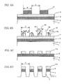
- FIGS. 2A to 2D a description will be given of the conventional technique for processing a width narrower than the minimum process size of F.
- a silicon nitride film 106 is deposited on a base layer 105 , and a mask pattern 107 of polysilicon is provided with a line width F and a space F.
- FIG. 2B after sidewalls 108 of silicon dioxide are formed on side walls, the mask pattern 107 is removed as shown in FIG. 2C . Then, the sidewalls 108 are used for the mask and the silicon nitride film 106 is etched.
- a line pattern 105 a with a width of x 1 which is narrower than the minimum process size of F, is created, thereby forming two types of spaces between the lines, F and xs, where xs is narrower than F.
- the lines are arranged at an average pitch of F, however, the line spaces are not uniform.
- F is the minimum width of the mask pattern used for forming the lines and F is the minimum space thereof. Therefore, it is impossible to accurately form lines haivng a width narrower than the aforementioned size with conventional fabrication techniques.
- conventional techniques for forming the line pattern of the pitch F the sidewall films formed on the side walls of the stripe pattern with the line width F and the space F are used for the mask, resulting in a constant line width.
- the line space has two types. That is, it is difficult to make a high-density pattern with line width and line space of equal sizes. Accordingly, it is also difficult to reduce the costs of the NAND-type flash memory in which high-density cell arrays are demanded in view of the limitations on the process size due to the performance limitations of photolithography.
- An object of the present invention is to solve the above-mentioned problems and provide a method for fabricating a highly integrated semiconductor device.
- a method for fabricating a semiconductor device including forming a first film on a base layer, forming a first mask pattern on the first film, the first mask pattern having mask portions arranged at a given pitch, forming first sidewall films on sidewalls of the first mask pattern by etchback of a deposited second film, removing the first mask pattern, and forming a second mask pattern composed of the first sidewall films and second sidewall films defined by etchback of a deposited third film.
- this first aspect of the present invention it is possible to form a stripe pattern with the line width and the line space having the same sizes at a pitch that is the same as the minimum process size determined by the photolithographic performance, thereby enabling the fabrication of a semiconductor device with a high degree of integration.
- a method for fabricating a semiconductor device including forming a first film and a second film on a base layer in that order, forming a first mask pattern on the second film, the first mask pattern having mask portions arranged at a given pitch, forming first sidewall films on sidewalls of the first mask pattern by etchback of a deposited third film, forming a second mask pattern by etching the second film with the first sidewall films being used as a mask after removing the first mask pattern, forming second sidewall films on both sides of the second mask pattern by etchback of a deposited fourth film after removing the first sidewall films, and etching the second sidewall films so that the second sidewall films remain only on one side of the second mask pattern so that a third mask pattern is composed of the remaining second sidewall films and the second mask pattern.
- this second aspect of the present invention it is also possible to form a stripe pattern with the line width and the line space having the same sizes at a pitch that is the same as the minimum process size determined by the photolithographic performance, thereby enabling the fabrication of a semiconductor device with a high degree of integration.
- FIG. 1 is a plane view of a conventional NAND-type flash memory array
- FIGS. 2A through 2D are cross-sectional views of a conventional semiconductor device during the fabrication process
- FIG. 3 is a plane view of a NAND-type flash memory array in accordance with a first embodiment of the present invention
- FIG. 4 is a cross-sectional view in accordance with the first embodiment of the present invention taken along a line A-A′ shown in FIG. 3 ;
- FIG. 5 is a cross-sectional view in accordance with the first embodiment of the present invention taken along a line B-B′ shown in FIG. 3 ;
- FIGS. 7F and 7G are cross-sectional views of the NAND-type flash memory array in accordance with the first embodiment of the present invention.
- FIG. 10 is a plane view of the NAND-type flash memory array in accordance with the second embodiment of the present invention.
- FIGS. 11A through 11E are cross-sectional views of the NAND-type flash memory array in accordance with a first variation example of the first embodiment of the present invention.
- FIGS. 13E through 13H are cross-sectional views of the NAND-type flash memory array in accordance with the second variation example of the first embodiment of the present invention.
- FIGS. 17E through 17H are cross-sectional views of the NAND-type flash memory array in accordance with the third variation example of the second embodiment of the present invention.
- FIGS. 18A through 18D are cross-sectional views of the NAND-type flash memory array in accordance with a fourth variation example of the second embodiment of the present invention.
- FIG. 19E is a cross-sectional view of the NAND-type flash memory array in accordance with the fourth variation example of the second embodiment of the present invention.
- the control gate 8 has a double-layer structure having a polysilicon film 8 a and a tungsten silicide layer 8 b corresponding to a word line.
- the bit line 10 is made of aluminum and formed on an interlayer insulating film (BPSG film) 9 made of BPSG (Boron Phosphorous Silicate Glass).
- BPSG film interlayer insulating film
- a barrier metal layer of Ti/TiN is formed below the aluminum of bit line 10 and an antireflection film of TiN layer is provided on the aluminum, however these are not shown in FIGS. 4 and 5 for simplification.
- the mask pattern (a first mask pattern) 12 with a line width and space of F is formed with polysilicon film with a thickness of approximately F/2.
- the mask pattern 12 is formed on the silicon nitride film 11 at a given pitch and is made of a polysilicon film.
- the mask pattern 12 may be any insulating film.
- a silicon dioxide film (a second film) 13 is deposited to the thickness of approximately F/4 by CVD (Chemical Vapor Deposition), and then, as shown in FIG. 6C , sidewall films (first sidewall films) 13 a are formed on side walls of the mask pattern 12 through etch back by RIE.
- sidewall films (second sidewall films) 14 a are formed on the vertical side surfaces of the sidewall films 13 a
- sidewall films (the second sidewall films) 14 b are formed on curved side surfaces of the sidewall films 13 a .
- the sidewall films 14 a are formed to have a bottom width of F/4
- the sidewall films 14 b are formed so that F/4 is a total of the bottom width of the sidewall films 13 a and the sidewall films 14 b .
- the bottom width of the sidewall film 14 a formed on the vertical side surface is substantially equal to a total of the bottom width of the sidewall film 14 b and the sidewall film 13 a .
- the sidewall film 14 b is formed thinner than the sidewall film 14 a . This is because the silicon dioxide film 14 is formed thicker on the vertical side surface of the sidewall film 13 a than on the curved side surface thereof.
- the silicon nitride film 11 is etched by RIE with the use of the mask pattern 15 .
- the mask pattern 15 of the silicon oxide film is selectively etched and removed in an etchant solution of HF (fluorinated acid) or the like.
- a resulting mask pattern (a third mask pattern) 11 a of the silicon nitride film is formed.
- the bit line 10 is formed by etching the Ti/TiN film 10 a , the aluminum film 10 b , and the TiN film 10 c , making up the base layer, by RIE with the use of the mask pattern 11 a .
- bit line 10 may be formed by etching the silicon nitride film 11 , the Ti/TiN film 10 a , the aluminum film 10 b , and the TiN film 10 c by RIE with the use of the mask pattern 15 .
- the bit line forming method in the NAND-type flash memory of the first embodiment it is possible to form a microscopic pattern in which the pitch is F and the line width and line space have the same sizes, in the photolithography method of the minimum process size of F.
- the present invention is not limited to the bit line of the NAND-type flash memory, and may be applicable also to the word line thereof. Moreover, the present invention is applicable to forming the microscopic line pattern of any other semiconductor device in addition to a memory.
- FIG. 8A there are provided the silicon dioxide film (a first gate insulating film) 5 to serve as a tunnel oxide film, the polysilicon film (a first conductive layer) 6 to serve as the floating gate, and the silicon nitride film 11 , which films are successively deposited on the silicon substrate 1 .
- the silicon dioxide film 5 and the polysilicon film 6 are base layers.
- the mask pattern 12 having the line width and space of the minimum process size of F is formed on the base layers with polysilicon film by the photolithography process.
- the mask pattern 15 is formed to have the line width of approximately F/2 and the space of approximately F/2 by using the sidewall films 13 a , 14 a , and 14 b.
- the mask pattern 15 of the silicon oxide film is etched away and removed in an etchant solution of HF or the like, and the mask pattern 11 a of the silicon nitride film is formed.
- the mask pattern 15 may remain without being etched.
- the polysilicon layer 6 , the silicon dioxide film 5 , and the silicon substrate 1 are etched by RIE to form the floating gate 6 and the trench 2 .
- etching proceeds to reach the silicon substrate 1 and forms the trench 2 therein.
- the depth of the trench 2 is determined by considering the punch-through resistance between elements adjacent to each other. It is desirable that the mask pattern 11 a should have a thickness determined in relationship to the depth of the trench 2 .
- a silicon dioxide film is then deposited to bury the trench 2 by CVD. It is desirable that TEOS (Tetra Ethyl Ortho Silicate) which exhibits excellent step coverage should be employed for the silicon dioxide film. Then, by CMP (Chemical Mechanical Polishing), the mask pattern 11 a of the silicon nitride. film is etched away and removed, and the silicon dioxide film buried in the trench forms STI 3 , as shown in FIG. 9E . Therefore, if it is desired that the mask pattern 15 should remain without being etched, a structure similar to that shown in FIG. 9E is obtainable by etching the silicon nitride film 11 and the base layer 10 to reach the silicon substrate 1 and forming the trench during the process of etching with the use of the mask pattern 15 .
- CMP Chemical Mechanical Polishing
- the silicon dioxide film in the vicinity of the surface of the STI 3 is etched in a diluted etchant solution of HF so that the exposed area of the floating gate 6 may be increased. This makes it possible to increase the coupling ratio between the floating gate 6 and the control gate 8 formed afterwards.
- the ONO stack 7 is formed as the second insulating film.
- the three ONO layers are shown as one layer for simplification.
- the polysilicon film 8 a and the tungsten silicide (WSi) film 8 b are sequentially deposited and processed by the photolithography process, thereby forming the control gate 8 .
- control gate 8 is formed in a known method to have the minimum process size of F. Then, the n-type diffusion layers to serve as the source/drain regions of the cell transistor are formed by ion implantation and the BPSG film 9 is deposited by CVD.
- a bit line and STI arranged at a pitch of F are obtainable.
- FIG. 14 is a plane view of the bit line contacts and the vicinity thereof in the NAND type flash memory array in accordance with the second embodiment of the present invention.
- a select gate 8 ′ is arranged on both sides of a pattern composed of a unit of sixteen word lines, not shown.
- the bit line 10 is in contact with the substrate, namely, a drain diffusion layer.
- the unit of sixteen word lines having the select gate 8 ′ on both sides thereof is arranged to establish a mirror symmetry sandwiching a common source region, the bit line contacts being provided on the edges thereof. Therefore, four select gates and thirty-two word lines are arranged between two contacts on the same bit line.
- FIG. 14 shows contact portions 22 of the bit line and one select gate 8 ′, for simplification. Adjacently provided bit lines are formed at a pitch of F and the contact portions are arranged in a zig-zag manner. This makes it possible to make a contact diameter of F and a space between the contact diameters at F in a conventional method.
- FIG. 15 is a cross-sectional view taken along a line C-C′ shown in FIG. 14 .
- a contact plug 23 of tungsten is provided inside the contact hole open through the BPSG 9 deposited on the substrate 1 with a diameter of F, so that the bit line 10 is connected to an n-type diffusion layer 24 serving as a drain region.
- the bit line contact is provided in a zig-zag manner, and the integration degree may be degraded slightly in the direction that the bit line extends.
- the peripheral circuit has to be formed in accordance with the memory cell array.
- the bit lines arranged at a small pitch it is possible to fabricate the circuit provided in the page buffer by a conventional method by arranging the page buffers on both sides of the memory array and arranging the bit lines to be alternately connected to both page buffers.
- the word line arranged at a small pitch As is well known, it is possible to fabricate the circuit of the decoder by arranging the word decoders on both sides of the memory array and connecting the several word lines as a unit to both decoders alternately.
- the word decoder is driven by a voltage Vpp higher than a voltage Vcc used in a peripheral circuit such as the page buffer, thereby requiring a large transistor size.
- FIG. 10 is a plane view of the NAND type flash memory that includes the word lines formed by the same fabrication method as described in regards to the first embodiment.
- One cell size is F 2 , and this size is one-fourth of that fabricated in the conventional fabrication method.
- the silicon nitride film 11 provided on the base layer has a non-uniform surface. That is to say, referring back to FIGS. 6A through 6E as described in the first embodiment, the surface of the silicon nitride film 11 is slightly etched in the process of forming and removing the mask pattern 12 and in the process of forming and removing the sidewall films 13 a , 14 a , and 14 b .
- the silicon nitride film 11 is used as the mask for fabricating the base layer by RIE.
- the mask pattern 12 has the etch selectivity for the silicon nitride film 11 to serve as the first film
- the silicon dioxide film 13 to serve as the second film has the etch selectivity for the silicon nitride film 11 to serve as the first film and the mask pattern 12
- the silicon oxide film 14 to serve as the third film has the etch selectivity for the nitride silicon film 11 to serve as the first film.
- the tungsten film 16 is used as a stopper film so that the silicon nitride film 11 provided on the base layer may not be etched during the etch process forming the mask pattern 15 .
- the tungsten film 16 is selected as a metal film that has a sufficient etch selectivity in relation to the polysilicon film 12 , the silicon dioxide films 13 and 14 , and the silicon nitride film 11 of the insulating films.
- any material may be employed instead of the tungsten film 16 , if it has sufficient etch selectivity in relation the insulating films.
- the tungsten film 16 and the silicon nitride film 11 may be etched using the mask pattern 15 by RIE. Then, the mask pattern 15 and the tungsten film 16 a that has been processed may be sequentially removed to form the mask pattern 11 a . Subsequently, the STI and the floating gate are created in the fabrication method as described in the second embodiment above.
- the fabrication method has been described heretofore for obtaining a microscopic pattern by making the mask pattern at a pitch of F, for a mask to be used for etching the base layer in the lithography process with the minimum process size of F.
- FIG. 12A On the silicon substrate 1 , the silicon dioxide film 5 serving as the tunnel oxide film and the polysilicon film 6 serving as the floating gate are deposited as the base layers.
- the silicon nitride film (the first film) 11 is formed on the base layer. The fabrication method heretofore is the same as described in the second embodiment.
- the bottom width of the sidewall film 20 is configured to be equal to the bottom width of the polysilicon film 16 a ( FIGS. 11C, 11D ), namely, equal to the bottom width sw of the sidewall film 19 illustrated in FIG. 12B .
- the bottom width sw is configured to be approximately F/4.
- photoresists 21 a and 21 b are sequentially applied on the polysilicon films 17 a , respective ends of which are adjacently arranged to each other, and are arranged alternately.
- a space F′ between the photoresists 21 a and 21 b is smaller than the minimum process size of F, so the photoresists 21 a and 21 b have to be formed separately and independently.
- the photoresists 21 a and 21 b can be aligned within a margin of the width of the polysilicon film 17 a (approximately F/4 in FIG. 13E ).
- the line width and space of the mask 18 are configured to be greater than F, enabling the formation of the photoresist 21 a and 21 b with a suitable margin.
- the pitch of the process pattern of the base layer obtainable in the end is greater than the aforementioned size of F.
- the sidewall films 20 are selectively etched with the photoresists 21 a and 21 b used for the masks, so that sidewall films 20 a only may remain on one of the side walls of the mask patterns 17 a .
- the photoresists 21 a and 21 b are removed so that the square-shaped polysilicon film 17 a with a width of approximately F/4 and a mask pattern (the third mask pattern) 15 ′ remain after the etch process.
- the mask pattern 15 ′ is formed on one of the side walls of the polysilicon film 17 a and is made up of the sidewall film 20 a with a bottom width of approximately F/4. Therefore, the bottom width of the mask pattern 17 a is configured to be substantially equal to that of the sidewall film 20 a that remains after the etch process, making the bottom width of the mask pattern 15 ′ approximately F/2.
- the mask pattern 15 ′ has the bottom width xl and the space xs, which are respectively equal to approximately F/2. However, it is possible to form the mask pattern 15 ′ to have a desired line width and space by adjusting the bottom widths sw thereof when the above-mentioned two sidewall films 19 and 20 are deposited.
- the silicon nitride film 11 is etched by RIE using the mask pattern 15 ′, and then the mask pattern 15 ′ is selectively etched to form a mask pattern (the fourth mask pattern) 11 a of the silicon nitride film.
- the silicon dioxide film 5 and the polysilicon film 6 serving as the base layers are etched with the mask pattern 11 a , and the STI and the floating gate are provided in the same fabrication method as described above in regards to the second embodiment of the present invention.
- the silicon nitride film 11 serving as the first film, the silicon dioxide film 5 serving as the base layer, and the polysilicon film 6 may be etched simultaneously by using the mask pattern 15 ′.
- the bottom width of the sidewall film 20 is configured to be equal to the bottom width of the polysilicon film 16 a ( FIGS. 11C and 11D ), namely, to be equal to the bottom width sw of the sidewall film 19 as illustrated in FIG. 12B .
- the bottom width sw is configured to be approximately F/4.
- the photoresists 21 a and 21 b are sequentially applied on the polysilicon films 17 a , respective ends of which are adjacently arranged to each other, and are arranged alternately.
- a space F′ between the photoresists 21 a and 21 b is smaller than the minimum process size of F, so the photoresists have to be made separately and independently.
- the photoresists 21 a and 21 b can be aligned within the margin of the width of the polysilicon film 17 a (approximately F/4 in FIG. 17E ).
- the silicon nitride film 11 is etched by RIE using the mask pattern 15 ′′, and then the mask pattern 15 ′′ is selectively etched to form a mask pattern 11 a of the silicon nitride film.
- the silicon dioxide film 5 and the polysilicon film 6 serving as the base layers are etched with the mask pattern 11 a , and the STI and the floating gate are created in the same fabrication method as described above in regards to the second embodiment of the present invention.
- the silicon nitride film 11 serving as the first film, the silicon dioxide film 5 serving as the base layer, and the polysilicon film 6 may be etched simultaneously by using the mask pattern 15 ′.
- the mask pattern at a pitch of F in an alternate fabrication method, different from the fabrication method described in accordance with the first and second embodiments.
- this method is applicable to processing any line such as the bit line.
- the mask 15 ′′′ of the silicon dioxide film is etched away in a HF solution.
- the silicon nitride film 11 is etched by RIE with the tungsten film 16 a that is exposed serving as the mask, and the mask pattern 11 a of the silicon nitride film is formed.
- the tungsten film 16 a is removed.
- the polysilicon film 6 , the second gate insulating film 7 , the polysilicon film 8 a , the tungsten silicide layer 8 b , and the silicon dioxide film 25 are etched.
- the mask pattern 11 a has been etched and removed during a CMP process.
- the n-type diffusion layers 4 serving as the source/drain regions of the cell transistor are formed by ion implantation in the surface of the silicon substrate 1 .
- the contacts are opened and the bit line 10 is formed in the method as described in regards to the first embodiment ( FIG. 5 ).
Landscapes
- Engineering & Computer Science (AREA)
- Microelectronics & Electronic Packaging (AREA)
- Condensed Matter Physics & Semiconductors (AREA)
- General Physics & Mathematics (AREA)
- Manufacturing & Machinery (AREA)
- Computer Hardware Design (AREA)
- Physics & Mathematics (AREA)
- Power Engineering (AREA)
- Chemical & Material Sciences (AREA)
- Inorganic Chemistry (AREA)
- Semiconductor Memories (AREA)
- Non-Volatile Memory (AREA)
- Internal Circuitry In Semiconductor Integrated Circuit Devices (AREA)
- Drying Of Semiconductors (AREA)
- Element Separation (AREA)
Abstract
Description
Claims (6)
Applications Claiming Priority (1)
| Application Number | Priority Date | Filing Date | Title |
|---|---|---|---|
| PCT/JP2004/019646 WO2006070474A1 (en) | 2004-12-28 | 2004-12-28 | Process for producing semiconductor device |
Related Parent Applications (1)
| Application Number | Title | Priority Date | Filing Date |
|---|---|---|---|
| PCT/JP2004/019646 Continuation WO2006070474A1 (en) | 2004-12-28 | 2004-12-28 | Process for producing semiconductor device |
Publications (2)
| Publication Number | Publication Date |
|---|---|
| US20060276032A1 US20060276032A1 (en) | 2006-12-07 |
| US9299578B2 true US9299578B2 (en) | 2016-03-29 |
Family
ID=36614601
Family Applications (1)
| Application Number | Title | Priority Date | Filing Date |
|---|---|---|---|
| US11/317,083 Active 2026-09-19 US9299578B2 (en) | 2004-12-28 | 2005-12-21 | Transistor formation method using sidewall masks |
Country Status (3)
| Country | Link |
|---|---|
| US (1) | US9299578B2 (en) |
| JP (1) | JPWO2006070474A1 (en) |
| WO (1) | WO2006070474A1 (en) |
Families Citing this family (19)
| Publication number | Priority date | Publication date | Assignee | Title |
|---|---|---|---|---|
| JP4866652B2 (en) * | 2006-05-10 | 2012-02-01 | ルネサスエレクトロニクス株式会社 | Semiconductor memory device |
| EP2472570A3 (en) * | 2006-08-16 | 2013-07-17 | SanDisk Technologies, Inc. | Nonvolatile memories with shaped floating gates |
| KR100762243B1 (en) * | 2006-09-19 | 2007-10-01 | 주식회사 하이닉스반도체 | Method for manufacturing of semiconductor device |
| KR100780774B1 (en) * | 2006-11-07 | 2007-11-30 | 주식회사 하이닉스반도체 | Nand type non-volatile memory device and method for fabricating the same |
| US7807575B2 (en) * | 2006-11-29 | 2010-10-05 | Micron Technology, Inc. | Methods to reduce the critical dimension of semiconductor devices |
| JP2008166518A (en) * | 2006-12-28 | 2008-07-17 | Toshiba Corp | Nonvolatile semiconductor memory device |
| US7842616B2 (en) | 2007-01-22 | 2010-11-30 | Advanced Technology Development Facility, Inc. | Methods for fabricating semiconductor structures |
| WO2008091343A1 (en) * | 2007-01-22 | 2008-07-31 | Atdf, Inc. | Methods for fabricating semiconductor structures |
| US7923373B2 (en) | 2007-06-04 | 2011-04-12 | Micron Technology, Inc. | Pitch multiplication using self-assembling materials |
| US7910976B2 (en) * | 2007-06-28 | 2011-03-22 | Richard Fastow | High density NOR flash array architecture |
| KR101271174B1 (en) * | 2007-08-03 | 2013-06-04 | 삼성전자주식회사 | Flash Memory Device improving a bit-line layout structure and Layout Method for the same |
| US7790531B2 (en) | 2007-12-18 | 2010-09-07 | Micron Technology, Inc. | Methods for isolating portions of a loop of pitch-multiplied material and related structures |
| JP5315689B2 (en) * | 2007-12-28 | 2013-10-16 | 東京エレクトロン株式会社 | Pattern forming method, semiconductor manufacturing apparatus, and storage medium |
| JP2009252830A (en) * | 2008-04-02 | 2009-10-29 | Toshiba Corp | Method of manufacturing semiconductor device |
| US8309462B1 (en) * | 2011-09-29 | 2012-11-13 | Sandisk Technologies Inc. | Double spacer quadruple patterning with self-connected hook-up |
| JP5738786B2 (en) * | 2012-02-22 | 2015-06-24 | 株式会社東芝 | Semiconductor device and manufacturing method of semiconductor device |
| JP2014053565A (en) * | 2012-09-10 | 2014-03-20 | Toshiba Corp | Semiconductor memory device and method of manufacturing the same |
| CN103715068A (en) * | 2012-09-29 | 2014-04-09 | 中芯国际集成电路制造(上海)有限公司 | Forming method of semiconductor fine pattern |
| CN104517813A (en) * | 2013-09-29 | 2015-04-15 | 中芯国际集成电路制造(上海)有限公司 | Method for forming double pattern |
Citations (13)
| Publication number | Priority date | Publication date | Assignee | Title |
|---|---|---|---|---|
| US4648937A (en) | 1985-10-30 | 1987-03-10 | International Business Machines Corporation | Method of preventing asymmetric etching of lines in sub-micrometer range sidewall images transfer |
| EP0402296A1 (en) | 1989-06-09 | 1990-12-12 | International Business Machines Corporation | Field-effect-transistor with asymmetrical structure |
| JPH07245402A (en) | 1994-03-04 | 1995-09-19 | Nippon Steel Corp | Manufacture of semiconductor device |
| JPH0855908A (en) | 1994-08-17 | 1996-02-27 | Toshiba Corp | Semiconductor device |
| JPH0855920A (en) | 1994-08-15 | 1996-02-27 | Toshiba Corp | Manufacture of semiconductor device |
| JPH10294367A (en) | 1997-04-21 | 1998-11-04 | Sony Corp | Manufacture of semiconductor device |
| JP2000173979A (en) | 1998-12-07 | 2000-06-23 | Sanyo Electric Co Ltd | Etching mask and method of forming fine pattern |
| US6872647B1 (en) * | 2003-05-06 | 2005-03-29 | Advanced Micro Devices, Inc. | Method for forming multiple fins in a semiconductor device |
| US6967140B2 (en) * | 2000-03-01 | 2005-11-22 | Intel Corporation | Quantum wire gate device and method of making same |
| US20050272259A1 (en) * | 2004-06-08 | 2005-12-08 | Macronix International Co., Ltd. | Method of pitch dimension shrinkage |
| US20060046422A1 (en) * | 2004-08-31 | 2006-03-02 | Micron Technology, Inc. | Methods for increasing photo alignment margins |
| US7435536B2 (en) * | 2004-09-02 | 2008-10-14 | Micron Technology, Inc. | Method to align mask patterns |
| US20100203727A1 (en) * | 2004-09-02 | 2010-08-12 | Micron Technology, Inc. | Method for integrated circuit fabrication using pitch multiplication |
-
2004
- 2004-12-28 WO PCT/JP2004/019646 patent/WO2006070474A1/en not_active Application Discontinuation
- 2004-12-28 JP JP2006550540A patent/JPWO2006070474A1/en active Pending
-
2005
- 2005-12-21 US US11/317,083 patent/US9299578B2/en active Active
Patent Citations (14)
| Publication number | Priority date | Publication date | Assignee | Title |
|---|---|---|---|---|
| US4648937A (en) | 1985-10-30 | 1987-03-10 | International Business Machines Corporation | Method of preventing asymmetric etching of lines in sub-micrometer range sidewall images transfer |
| EP0402296A1 (en) | 1989-06-09 | 1990-12-12 | International Business Machines Corporation | Field-effect-transistor with asymmetrical structure |
| JPH0323673A (en) | 1989-06-09 | 1991-01-31 | Internatl Business Mach Corp <Ibm> | Field-effect transistor having asymmetric structure and manufacture thereof |
| JPH07245402A (en) | 1994-03-04 | 1995-09-19 | Nippon Steel Corp | Manufacture of semiconductor device |
| JPH0855920A (en) | 1994-08-15 | 1996-02-27 | Toshiba Corp | Manufacture of semiconductor device |
| JPH0855908A (en) | 1994-08-17 | 1996-02-27 | Toshiba Corp | Semiconductor device |
| JPH10294367A (en) | 1997-04-21 | 1998-11-04 | Sony Corp | Manufacture of semiconductor device |
| JP2000173979A (en) | 1998-12-07 | 2000-06-23 | Sanyo Electric Co Ltd | Etching mask and method of forming fine pattern |
| US6967140B2 (en) * | 2000-03-01 | 2005-11-22 | Intel Corporation | Quantum wire gate device and method of making same |
| US6872647B1 (en) * | 2003-05-06 | 2005-03-29 | Advanced Micro Devices, Inc. | Method for forming multiple fins in a semiconductor device |
| US20050272259A1 (en) * | 2004-06-08 | 2005-12-08 | Macronix International Co., Ltd. | Method of pitch dimension shrinkage |
| US20060046422A1 (en) * | 2004-08-31 | 2006-03-02 | Micron Technology, Inc. | Methods for increasing photo alignment margins |
| US7435536B2 (en) * | 2004-09-02 | 2008-10-14 | Micron Technology, Inc. | Method to align mask patterns |
| US20100203727A1 (en) * | 2004-09-02 | 2010-08-12 | Micron Technology, Inc. | Method for integrated circuit fabrication using pitch multiplication |
Non-Patent Citations (4)
| Title |
|---|
| Aritome et al.; "A 0.67 um2 Self-Aligned Shallow Trench Isolation Cell (Sa-Sti Cell) for 3V-only 256Mbit Nand Eeproms.", 1994 IEEE; IEDM 94-61; pp. 3.6.1-3.6.4. |
| International Search Report for International Application No. PCT/JP04/19646 dated Apr. 19, 2005; 4 pages. |
| Sung et al.; "Fabrication and Program/Erase Characteristics of 30-nm SONOS Novolatile Memory Devices", 2003 IEEE Trjansactions on Nanotechnology, vol. 2, No. 4, Dec. 2003. |
| Written Opinion of the International Searching Authority for International Application No. PCT/JP04/19646 dated Apr. 19, 2005; 3 pages. |
Also Published As
| Publication number | Publication date |
|---|---|
| JPWO2006070474A1 (en) | 2008-06-12 |
| US20060276032A1 (en) | 2006-12-07 |
| WO2006070474A1 (en) | 2006-07-06 |
Similar Documents
| Publication | Publication Date | Title |
|---|---|---|
| US9299578B2 (en) | Transistor formation method using sidewall masks | |
| US6593190B2 (en) | Non-volatile memory device having a bit line contact pad and method for manufacturing the same | |
| US7795080B2 (en) | Methods of forming integrated circuit devices using composite spacer structures | |
| US8809146B2 (en) | Semiconductor devices comprising a plurality of gate structures | |
| US6372651B1 (en) | Method for trimming a photoresist pattern line for memory gate etching | |
| US7482630B2 (en) | NAND memory arrays | |
| US8436410B2 (en) | Semiconductor devices comprising a plurality of gate structures | |
| US7745325B2 (en) | Wiring structure of a semiconductor device, method of forming the wiring structure, non-volatile memory device including the wiring structure, and method of manufacturing the non-volatile memory device | |
| US7768061B2 (en) | Self aligned 1 bit local SONOS memory cell | |
| US7773403B2 (en) | Spacer patterns using assist layer for high density semiconductor devices | |
| US7683422B2 (en) | Non-volatile memory devices with wraparound-shaped floating gate electrodes and methods of forming same | |
| US20050196913A1 (en) | Floating gate memory structures and fabrication methods | |
| US8716119B2 (en) | Methods of forming transistor gates | |
| KR20080033845A (en) | A stacked thin film transistor, non-volatile memory devices and methods for fabricating the same | |
| US20050212032A1 (en) | Fabrication of conductive lines interconnecting first conductive gates in nonvolatile memories having second conductive gates provided by conductive gate lines, wherein the adjacent conductive gate lines for the adjacent columns are spaced from each other, and non-volatile memory structures | |
| US20070087502A1 (en) | Method of forming FLASH cell array having reduced word line pitch | |
| US9099532B2 (en) | Processes for NAND flash memory fabrication | |
| US8952536B2 (en) | Semiconductor device and method of fabrication | |
| US7602005B2 (en) | Memory devices including spacer-shaped electrodes on pedestals and methods of manufacturing the same | |
| JP5281770B2 (en) | Semiconductor device and manufacturing method thereof | |
| US20070138538A1 (en) | Method of forming self-aligned floating gate array and flash memory device including self-aligned floating gate array |
Legal Events
| Date | Code | Title | Description |
|---|---|---|---|
| AS | Assignment |
Owner name: SPANSION LLC, CALIFORNIA Free format text: ASSIGNMENT OF ASSIGNORS INTEREST;ASSIGNORS:ARAKAWA, HIDEKI;ITO, TAKUO;REEL/FRAME:018117/0206;SIGNING DATES FROM 20060530 TO 20060606 Owner name: SPANSION LLC, CALIFORNIA Free format text: ASSIGNMENT OF ASSIGNORS INTEREST;ASSIGNORS:ARAKAWA, HIDEKI;ITO, TAKUO;SIGNING DATES FROM 20060530 TO 20060606;REEL/FRAME:018117/0206 |
|
| AS | Assignment |
Owner name: BARCLAYS BANK PLC,NEW YORK Free format text: SECURITY AGREEMENT;ASSIGNORS:SPANSION LLC;SPANSION INC.;SPANSION TECHNOLOGY INC.;AND OTHERS;REEL/FRAME:024522/0338 Effective date: 20100510 Owner name: BARCLAYS BANK PLC, NEW YORK Free format text: SECURITY AGREEMENT;ASSIGNORS:SPANSION LLC;SPANSION INC.;SPANSION TECHNOLOGY INC.;AND OTHERS;REEL/FRAME:024522/0338 Effective date: 20100510 |
|
| AS | Assignment |
Owner name: SPANSION INC., CALIFORNIA Free format text: RELEASE BY SECURED PARTY;ASSIGNOR:BARCLAYS BANK PLC;REEL/FRAME:035201/0159 Effective date: 20150312 Owner name: SPANSION LLC, CALIFORNIA Free format text: RELEASE BY SECURED PARTY;ASSIGNOR:BARCLAYS BANK PLC;REEL/FRAME:035201/0159 Effective date: 20150312 Owner name: SPANSION TECHNOLOGY LLC, CALIFORNIA Free format text: RELEASE BY SECURED PARTY;ASSIGNOR:BARCLAYS BANK PLC;REEL/FRAME:035201/0159 Effective date: 20150312 |
|
| AS | Assignment |
Owner name: MORGAN STANLEY SENIOR FUNDING, INC., NEW YORK Free format text: SECURITY INTEREST;ASSIGNORS:CYPRESS SEMICONDUCTOR CORPORATION;SPANSION LLC;REEL/FRAME:035240/0429 Effective date: 20150312 |
|
| AS | Assignment |
Owner name: CYPRESS SEMICONDUCTOR CORPORATION, CALIFORNIA Free format text: ASSIGNMENT OF ASSIGNORS INTEREST;ASSIGNOR:SPANSION LLC;REEL/FRAME:035888/0807 Effective date: 20150601 |
|
| STCF | Information on status: patent grant |
Free format text: PATENTED CASE |
|
| MAFP | Maintenance fee payment |
Free format text: PAYMENT OF MAINTENANCE FEE, 4TH YEAR, LARGE ENTITY (ORIGINAL EVENT CODE: M1551); ENTITY STATUS OF PATENT OWNER: LARGE ENTITY Year of fee payment: 4 |
|
| AS | Assignment |
Owner name: MUFG UNION BANK, N.A., CALIFORNIA Free format text: ASSIGNMENT AND ASSUMPTION OF SECURITY INTEREST IN INTELLECTUAL PROPERTY;ASSIGNOR:MORGAN STANLEY SENIOR FUNDING, INC.;REEL/FRAME:050896/0366 Effective date: 20190731 |
|
| AS | Assignment |
Owner name: MORGAN STANLEY SENIOR FUNDING, INC., NEW YORK Free format text: CORRECTIVE ASSIGNMENT TO CORRECT THE 8647899 PREVIOUSLY RECORDED ON REEL 035240 FRAME 0429. ASSIGNOR(S) HEREBY CONFIRMS THE SECURITY INTERST;ASSIGNORS:CYPRESS SEMICONDUCTOR CORPORATION;SPANSION LLC;REEL/FRAME:058002/0470 Effective date: 20150312 |
|
| AS | Assignment |
Owner name: SPANSION LLC, CALIFORNIA Free format text: RELEASE BY SECURED PARTY;ASSIGNOR:MUFG UNION BANK, N.A.;REEL/FRAME:059410/0438 Effective date: 20200416 Owner name: CYPRESS SEMICONDUCTOR CORPORATION, CALIFORNIA Free format text: RELEASE BY SECURED PARTY;ASSIGNOR:MUFG UNION BANK, N.A.;REEL/FRAME:059410/0438 Effective date: 20200416 |
|
| AS | Assignment |
Owner name: INFINEON TECHNOLOGIES LLC, CALIFORNIA Free format text: ASSIGNMENT OF ASSIGNORS INTEREST;ASSIGNOR:CYPRESS SEMICONDUCTOR CORPORATION;REEL/FRAME:059721/0467 Effective date: 20200315 |
|
| MAFP | Maintenance fee payment |
Free format text: PAYMENT OF MAINTENANCE FEE, 8TH YEAR, LARGE ENTITY (ORIGINAL EVENT CODE: M1552); ENTITY STATUS OF PATENT OWNER: LARGE ENTITY Year of fee payment: 8 |