US9299290B2 - Display device and control method thereof - Google Patents
Display device and control method thereof Download PDFInfo
- Publication number
- US9299290B2 US9299290B2 US14/359,940 US201114359940A US9299290B2 US 9299290 B2 US9299290 B2 US 9299290B2 US 201114359940 A US201114359940 A US 201114359940A US 9299290 B2 US9299290 B2 US 9299290B2
- Authority
- US
- United States
- Prior art keywords
- electrode
- voltage
- drive transistor
- pixel circuit
- power source
- Prior art date
- Legal status (The legal status is an assumption and is not a legal conclusion. Google has not performed a legal analysis and makes no representation as to the accuracy of the status listed.)
- Active, expires
Links
Images


Classifications
-
- G—PHYSICS
- G09—EDUCATION; CRYPTOGRAPHY; DISPLAY; ADVERTISING; SEALS
- G09G—ARRANGEMENTS OR CIRCUITS FOR CONTROL OF INDICATING DEVICES USING STATIC MEANS TO PRESENT VARIABLE INFORMATION
- G09G3/00—Control arrangements or circuits, of interest only in connection with visual indicators other than cathode-ray tubes
- G09G3/20—Control arrangements or circuits, of interest only in connection with visual indicators other than cathode-ray tubes for presentation of an assembly of a number of characters, e.g. a page, by composing the assembly by combination of individual elements arranged in a matrix no fixed position being assigned to or needed to be assigned to the individual characters or partial characters
- G09G3/22—Control arrangements or circuits, of interest only in connection with visual indicators other than cathode-ray tubes for presentation of an assembly of a number of characters, e.g. a page, by composing the assembly by combination of individual elements arranged in a matrix no fixed position being assigned to or needed to be assigned to the individual characters or partial characters using controlled light sources
- G09G3/30—Control arrangements or circuits, of interest only in connection with visual indicators other than cathode-ray tubes for presentation of an assembly of a number of characters, e.g. a page, by composing the assembly by combination of individual elements arranged in a matrix no fixed position being assigned to or needed to be assigned to the individual characters or partial characters using controlled light sources using electroluminescent panels
- G09G3/32—Control arrangements or circuits, of interest only in connection with visual indicators other than cathode-ray tubes for presentation of an assembly of a number of characters, e.g. a page, by composing the assembly by combination of individual elements arranged in a matrix no fixed position being assigned to or needed to be assigned to the individual characters or partial characters using controlled light sources using electroluminescent panels semiconductive, e.g. using light-emitting diodes [LED]
- G09G3/3208—Control arrangements or circuits, of interest only in connection with visual indicators other than cathode-ray tubes for presentation of an assembly of a number of characters, e.g. a page, by composing the assembly by combination of individual elements arranged in a matrix no fixed position being assigned to or needed to be assigned to the individual characters or partial characters using controlled light sources using electroluminescent panels semiconductive, e.g. using light-emitting diodes [LED] organic, e.g. using organic light-emitting diodes [OLED]
- G09G3/3225—Control arrangements or circuits, of interest only in connection with visual indicators other than cathode-ray tubes for presentation of an assembly of a number of characters, e.g. a page, by composing the assembly by combination of individual elements arranged in a matrix no fixed position being assigned to or needed to be assigned to the individual characters or partial characters using controlled light sources using electroluminescent panels semiconductive, e.g. using light-emitting diodes [LED] organic, e.g. using organic light-emitting diodes [OLED] using an active matrix
- G09G3/3233—Control arrangements or circuits, of interest only in connection with visual indicators other than cathode-ray tubes for presentation of an assembly of a number of characters, e.g. a page, by composing the assembly by combination of individual elements arranged in a matrix no fixed position being assigned to or needed to be assigned to the individual characters or partial characters using controlled light sources using electroluminescent panels semiconductive, e.g. using light-emitting diodes [LED] organic, e.g. using organic light-emitting diodes [OLED] using an active matrix with pixel circuitry controlling the current through the light-emitting element
-
- G—PHYSICS
- G09—EDUCATION; CRYPTOGRAPHY; DISPLAY; ADVERTISING; SEALS
- G09G—ARRANGEMENTS OR CIRCUITS FOR CONTROL OF INDICATING DEVICES USING STATIC MEANS TO PRESENT VARIABLE INFORMATION
- G09G3/00—Control arrangements or circuits, of interest only in connection with visual indicators other than cathode-ray tubes
- G09G3/20—Control arrangements or circuits, of interest only in connection with visual indicators other than cathode-ray tubes for presentation of an assembly of a number of characters, e.g. a page, by composing the assembly by combination of individual elements arranged in a matrix no fixed position being assigned to or needed to be assigned to the individual characters or partial characters
- G09G3/22—Control arrangements or circuits, of interest only in connection with visual indicators other than cathode-ray tubes for presentation of an assembly of a number of characters, e.g. a page, by composing the assembly by combination of individual elements arranged in a matrix no fixed position being assigned to or needed to be assigned to the individual characters or partial characters using controlled light sources
- G09G3/30—Control arrangements or circuits, of interest only in connection with visual indicators other than cathode-ray tubes for presentation of an assembly of a number of characters, e.g. a page, by composing the assembly by combination of individual elements arranged in a matrix no fixed position being assigned to or needed to be assigned to the individual characters or partial characters using controlled light sources using electroluminescent panels
- G09G3/32—Control arrangements or circuits, of interest only in connection with visual indicators other than cathode-ray tubes for presentation of an assembly of a number of characters, e.g. a page, by composing the assembly by combination of individual elements arranged in a matrix no fixed position being assigned to or needed to be assigned to the individual characters or partial characters using controlled light sources using electroluminescent panels semiconductive, e.g. using light-emitting diodes [LED]
- G09G3/3208—Control arrangements or circuits, of interest only in connection with visual indicators other than cathode-ray tubes for presentation of an assembly of a number of characters, e.g. a page, by composing the assembly by combination of individual elements arranged in a matrix no fixed position being assigned to or needed to be assigned to the individual characters or partial characters using controlled light sources using electroluminescent panels semiconductive, e.g. using light-emitting diodes [LED] organic, e.g. using organic light-emitting diodes [OLED]
- G09G3/3225—Control arrangements or circuits, of interest only in connection with visual indicators other than cathode-ray tubes for presentation of an assembly of a number of characters, e.g. a page, by composing the assembly by combination of individual elements arranged in a matrix no fixed position being assigned to or needed to be assigned to the individual characters or partial characters using controlled light sources using electroluminescent panels semiconductive, e.g. using light-emitting diodes [LED] organic, e.g. using organic light-emitting diodes [OLED] using an active matrix
- G09G3/3258—Control arrangements or circuits, of interest only in connection with visual indicators other than cathode-ray tubes for presentation of an assembly of a number of characters, e.g. a page, by composing the assembly by combination of individual elements arranged in a matrix no fixed position being assigned to or needed to be assigned to the individual characters or partial characters using controlled light sources using electroluminescent panels semiconductive, e.g. using light-emitting diodes [LED] organic, e.g. using organic light-emitting diodes [OLED] using an active matrix with pixel circuitry controlling the voltage across the light-emitting element
-
- H01L27/3244—
-
- G—PHYSICS
- G09—EDUCATION; CRYPTOGRAPHY; DISPLAY; ADVERTISING; SEALS
- G09G—ARRANGEMENTS OR CIRCUITS FOR CONTROL OF INDICATING DEVICES USING STATIC MEANS TO PRESENT VARIABLE INFORMATION
- G09G2300/00—Aspects of the constitution of display devices
- G09G2300/08—Active matrix structure, i.e. with use of active elements, inclusive of non-linear two terminal elements, in the pixels together with light emitting or modulating elements
- G09G2300/0809—Several active elements per pixel in active matrix panels
- G09G2300/0819—Several active elements per pixel in active matrix panels used for counteracting undesired variations, e.g. feedback or autozeroing
-
- G—PHYSICS
- G09—EDUCATION; CRYPTOGRAPHY; DISPLAY; ADVERTISING; SEALS
- G09G—ARRANGEMENTS OR CIRCUITS FOR CONTROL OF INDICATING DEVICES USING STATIC MEANS TO PRESENT VARIABLE INFORMATION
- G09G2300/00—Aspects of the constitution of display devices
- G09G2300/08—Active matrix structure, i.e. with use of active elements, inclusive of non-linear two terminal elements, in the pixels together with light emitting or modulating elements
- G09G2300/0809—Several active elements per pixel in active matrix panels
- G09G2300/0842—Several active elements per pixel in active matrix panels forming a memory circuit, e.g. a dynamic memory with one capacitor
- G09G2300/0852—Several active elements per pixel in active matrix panels forming a memory circuit, e.g. a dynamic memory with one capacitor being a dynamic memory with more than one capacitor
-
- G—PHYSICS
- G09—EDUCATION; CRYPTOGRAPHY; DISPLAY; ADVERTISING; SEALS
- G09G—ARRANGEMENTS OR CIRCUITS FOR CONTROL OF INDICATING DEVICES USING STATIC MEANS TO PRESENT VARIABLE INFORMATION
- G09G2300/00—Aspects of the constitution of display devices
- G09G2300/08—Active matrix structure, i.e. with use of active elements, inclusive of non-linear two terminal elements, in the pixels together with light emitting or modulating elements
- G09G2300/0809—Several active elements per pixel in active matrix panels
- G09G2300/0842—Several active elements per pixel in active matrix panels forming a memory circuit, e.g. a dynamic memory with one capacitor
- G09G2300/0861—Several active elements per pixel in active matrix panels forming a memory circuit, e.g. a dynamic memory with one capacitor with additional control of the display period without amending the charge stored in a pixel memory, e.g. by means of additional select electrodes
-
- G—PHYSICS
- G09—EDUCATION; CRYPTOGRAPHY; DISPLAY; ADVERTISING; SEALS
- G09G—ARRANGEMENTS OR CIRCUITS FOR CONTROL OF INDICATING DEVICES USING STATIC MEANS TO PRESENT VARIABLE INFORMATION
- G09G2320/00—Control of display operating conditions
- G09G2320/02—Improving the quality of display appearance
- G09G2320/0223—Compensation for problems related to R-C delay and attenuation in electrodes of matrix panels, e.g. in gate electrodes or on-substrate video signal electrodes
-
- H—ELECTRICITY
- H10—SEMICONDUCTOR DEVICES; ELECTRIC SOLID-STATE DEVICES NOT OTHERWISE PROVIDED FOR
- H10K—ORGANIC ELECTRIC SOLID-STATE DEVICES
- H10K59/00—Integrated devices, or assemblies of multiple devices, comprising at least one organic light-emitting element covered by group H10K50/00
- H10K59/10—OLED displays
- H10K59/12—Active-matrix OLED [AMOLED] displays
Definitions
- the present invention relates to a display device and a method of controlling the display device.
- the active-matrix organic EL display devices which have been put into practical implementation have a structure (cathode common structure) in which cathode electrodes of organic EL elements of respective pixels have a common potential. Furthermore, drive circuits for controlling the light emission of these organic EL elements are generally configured of P-type thin film transistors (TFT).
- TFT P-type thin film transistors
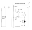
- the pixel circuit 90 is supplied with a control signal from a scanning line drive circuit 4 via a signal line SCAN, and supplied with a data voltage corresponding to a light-emitting luminance from a signal line drive circuit 5 via a data line DATA. Furthermore, a power source voltage for use in the light emission by the organic EL element EL is supplied to the pixel circuit 90 from a power source circuit not shown in the Drawing via power source lines VDD and VSS.
- FIG. 21 is a timing chart showing an example of the control signal, data voltage, and power source voltage for operating the pixel circuit 90 , for one-frame period.
- the vertical axis denotes the level of each signal, and the horizontal axis represents the passing of time.
- the control signal, the data voltage, and the power source voltage are given the same names as the respective signal lines and power source lines through which they are transmitted.
- the pixel circuit 90 repeats a Vth detecting step, a data writing step, a resetting step, and a light-emitting step, on a frame basis, according to the control signal, power source voltage, and data signal shown in FIG. 21 .
- FIG. 22 (a) to (d) are circuit diagrams for describing the operation on the pixel circuit 90 in the Vth detecting step, the data writing step, the resetting step, and the light-emitting step, respectively.
- the power source voltage VDD is set to 0
- the power source voltage VSS is set to V E2
- the data voltage DATA is set to V DH .
- the threshold voltage Vth is held by the capacitor Cs based on the voltage V DH obtained from the data line DATA.
- the drive transistor TD is turned into ON state by the differential voltage between the voltage of the gate electrode and the power source voltage VDD, and the anode voltage of the organic EL element EL is initialized to ⁇ V E1 .
- the power source voltage VSS is set to ⁇ V EE
- the voltage of the source electrode of the drive transistor TD becomes a voltage V EE +V EL obtained by adding the power source voltage VSS and the ON voltage of the organic EL element EL.
- the voltage which is (1 ⁇ ) ⁇ Vdata+Vth ⁇ (V EE +V EL ) is applied between the gate electrode and the source electrode of the drive transistor TD.
- a current i pix ⁇ /2((1 ⁇ ) ⁇ Vdata ⁇ (V EE +V EL )) 2 , which does not include the term representing the threshold voltage Vth of the drive transistor TD, is supplied from the drive transistor TD to the organic EL element EL.
- the organic EL element EL emits light at the luminance corresponding to the magnitude of the current i pix .
- the pixel circuit 90 reduces the effect of the threshold voltage Vth considerably by the Vth detection operation, and makes it possible for the organic EL element EL to emit light at a more accurate and stable luminance.
- the conventional pixel circuit 90 excludes, by elegantly using the reverse bias characteristics of the cathode-common organic EL element, the term of threshold voltage Vth of the drive transistor TD from the magnitude of the current i pix that is to be supplied from the drive transistor TD to the organic EL element EL. This allows the organic EL element EL to emit light at a luminance not affected by the change in the threshold voltage Vth of the drive transistor TD.
- the pixel circuit 90 has at least three error causes remained which lower the accuracy of the light-emitting luminance of the organic EL element EL.
- the first error cause is that the magnitude of the current i pix depends on the power source voltage VSS. If the power source voltage VSS is correctly set to ⁇ V EE , the correct light-emitting luminance can be obtained. However, in the power source line VSS that transmits a large current for use in light emission by the organic EL element EL, a complicated voltage drop that varies according to the light-emitting luminance occurs due to the wiring resistance of the power source line VSS itself. Thus, it cannot be practically expected that the voltage of the connecting point of the power source line VSS and the pixel circuit 90 is correctly set to ⁇ V EE in the light-emission period. Errors in the power source voltage VSS are reflected to errors in the light-emitting luminance of the organic EL element EL.
- the second error cause is that the magnitude of the current i pix depends on the drive voltage of the organic EL element EL.
- the current flowing in the organic EL element EL for light emission causes stress which deteriorates the organic EL element EL itself, lowers the light-emission efficiency due to aging, and varies its electrical characteristics.
- the drive voltage of the organic EL element EL required for flowing the same magnitude of current increases due to aging. Specifically, the deterioration in pixel luminance due to aging is caused not only by the deterioration in light-emission efficiency of the organic EL element EL but also by the increase in drive voltage. This makes the deterioration more visible.
- the third error cause is that the magnitude of the current i pix depends on the ratio ⁇ between the capacitance of the capacitor Cs and the parasitic capacitance of the organic EL element EL.
- the accuracy of the parasitic capacitance of the organic EL element EL is inferior to the accuracy of the capacitance of the capacitor formed intentionally.
- the ratio ⁇ includes considerable degree of errors. Errors in the ratio ⁇ are reflected to errors in the light-emitting luminance of the organic EL element EL.
- the present invention has been made to solve the above issues, and has an object to provide a display device including a pixel circuit capable of causing an organic EL element to emit light at a more accurate and stable luminance and the control method of the display device.
- a display device including a display unit having a plurality of pixel circuits each of which includes: a drive transistor having a drain electrode and a source electrode, one of the drain electrode and the source electrode being connected to a first power source line that transmits a first power source voltage; a first capacitive element having a first electrode connected to a gate electrode of the drive transistor and a second electrode connected to the source electrode of the drive transistor; a second capacitive element having a first electrode connected to the second electrode of the first capacitive element and a second electrode connected to a data line that transmits a data voltage corresponding to a luminance; a first switching element that switches between conduction and non-conduction between the gate electrode of the drive transistor and a reference voltage line that transmits a fixed reference voltage; and a light-emitting device having a first electrode connected to an other of the drain electrode and the source electrode of the drive transistor and a second electrode connected to a second power source
- the effect of the threshold voltage Vth is significantly reduced by performing the Vth detection operation and reset operation, in the same manner as in the conventional pixel circuit.
- the data voltage held by the first capacitive element is applied between the gate electrode and the source electrode of the drive transistor, and thus the magnitude of the current supplied from the drive transistor to the light-emitting device is not affected by the power source voltage. In other words, the above-described first and second error causes are eliminated.
- the data voltage held by the first capacitive element is determined according to the capacitance ratio between the first capacitive element and the second capacitive element.
- the data voltage can be set to the first capacitive element more accurately than in the conventional technique which uses the parasitic capacitance of the light-emitting device. In other words, the above-described third error cause is eliminated.
- FIG. 1 is a function block diagram showing an example of a configuration of a display device according to Embodiment 1.
- FIG. 2 is a circuit diagram showing an example of a configuration of a pixel circuit according to Embodiment 1.
- FIG. 3 is a timing chart showing an example of a control signal, power source voltage, and data signal according to Embodiment 1.
- FIGS. 4( a )-( d ) are circuit diagrams showing an example of the operation on a pixel circuit according to Embodiment 1.
- FIG. 5 is a circuit diagram showing an example of a configuration of a pixel circuit according to Embodiment 2.
- FIG. 6 is a timing chart showing an example of a control signal, power source voltage, and data signal according to Embodiment 2.
- FIGS. 7( a )-( d ) are circuit diagrams showing an example of the operation on a pixel circuit according to Embodiment 2.
- FIG. 8 is a circuit diagram showing an example of a configuration of a pixel circuit according to a modification of Embodiment 2.
- FIG. 9 is a circuit diagram showing an example of a configuration of a pixel circuit according to the modification of Embodiment 2.
- FIG. 10 is a circuit diagram showing an example of a configuration of a pixel circuit according to Embodiment 3.
- FIG. 11 is a circuit diagram showing an example of a configuration of a pixel circuit according to Embodiment 4.
- FIG. 12 is a timing chart showing an example of a control signal, power source voltage, and data signal according to Embodiment 4.
- FIG. 13 is a timing chart showing another example of a control signal, power source voltage, and data signal according to Embodiment 4.
- FIG. 14 is a circuit diagram showing an example of a configuration of a pixel circuit according to Embodiment 5.
- FIG. 15 is a timing chart showing an example of a control signal, power source voltage, and data signal according to Embodiment 5.
- FIG. 16 is a circuit diagram showing an example of a configuration of a pixel circuit according to Embodiment 6.
- FIG. 17 is a timing chart showing an example of a control signal, power source voltage, and data signal according to Embodiment 6.
- FIG. 18 is a timing chart showing another example of a control signal, power source voltage, and data signal according to Embodiment 6.
- FIG. 19 is an external appearance showing an example of a thin flat TV having the display device according to the present invention.
- FIG. 20 is a circuit diagram showing an example of a configuration of a conventional pixel circuit.
- FIG. 21 is a timing chart showing an example of a conventional control signal, power source voltage, and data signal.
- FIGS. 22( a )-( d ) are circuit diagrams showing an example of the operation on the conventional pixel circuit.
- a display device is a display device including a display unit having a plurality of pixel circuits each of which includes: a drive transistor having a drain electrode and a source electrode, one of the drain electrode and the source electrode being connected to a first power source line that transmits a first power source voltage; a first capacitive element having a first electrode connected to a gate electrode of the drive transistor and a second electrode connected to the source electrode of the drive transistor; a second capacitive element having a first electrode connected to the second electrode of the first capacitive element and a second electrode connected to a data line that transmits a data voltage corresponding to a luminance; a first switching element that switches between conduction and non-conduction between the gate electrode of the drive transistor and a reference voltage line that transmits a fixed reference voltage; and a light-emitting device having a first electrode connected to an other of the drain electrode and the source electrode of the drive transistor and a second electrode connected to a second power source line that transmits a second power source
- the second electrode of the second capacitive element may be directly connected to the data line.
- the data voltage held by the first capacitance element is applied between the gate electrode and the source electrode of the drive transistor, and thus the magnitude of the current supplied from the drive transistor to the light-emitting device is not affected by the power source voltage.
- the data voltage held by the first capacitive element is determined according to the capacitance ratio between the first capacitive element and the second capacitive element.
- the data voltage can be set to the first capacitive element more accurately than in the conventional technique which uses the parasitic capacitance of the light-emitting device.
- the organic EL element EL it is possible to cause the organic EL element EL to emit light at a more accurate and stable luminance than in the conventional technique.
- each of the pixel circuits may further include a second switching element provided between the source electrode of the drive transistor and the second electrode of the first capacitive element.
- the source electrode of the drive transistor and the second electrode of the first capacitive element can be electrically separated, which eliminates the concern on the change in the data voltage held by the first capacitive element along with the voltage change in the source electrode of the drive transistor.
- the organic EL element EL it is possible to cause the organic EL element EL to emit light with a more accurate and stable luminance.
- each of the pixel circuits may further include a third switching element provided between the first power source line and the one of the drain electrode and the source electrode of the drive transistor.
- the light-emission operation can be started all together for the pixel circuits of all of the rows using the third switching elements. This prevents the pixel current in the pixel circuit which started the light-emission operation earlier from being unstable during the writing operation on the pixel circuits of other rows. Thus, an excellent display image quality can be realized.
- each of the pixel circuits may further include a fourth switching element provided between the data line and the second electrode of the second capacitive element.
- the pixel circuit can be electrically separated from the data line at least in the light-emission period, which prevents the pixel current in the pixel circuit which started the light-emission operation earlier from being unstable during the writing operation on other rows.
- an excellent visual quality can be realized.
- a control method is a method of controlling a display device including a display unit having a plurality of pixel circuits each of which includes: a drive transistor having a drain electrode and a source electrode, one of the drain electrode and the source electrode being connected to a first power source line that transmits a first power source voltage; a first capacitive element having a first electrode connected to a gate electrode of the drive transistor and a second electrode connected to the source electrode of the drive transistor; a second capacitive element having a first electrode connected to the second electrode of the first capacitive element and a second electrode connected to a data line that transmits a data voltage corresponding to a luminance; a first switching element that switches between conduction and non-conduction between the gate electrode of the drive transistor and a reference voltage line that transmits a fixed reference voltage; and a light-emitting device having a first electrode connected to the other of the drain electrode and the source electrode of the drive transistor and a second electrode connected to a second power source line that transmits
- each of the pixel circuits may further include a second switching element provided between the source electrode of the drive transistor and the second electrode of the first capacitive element
- the method of controlling the display device may further include, in each of the pixel circuits, switching the second switching element to the non-conducting state, and holding the data voltage by the first capacitive element and the second capacitive element.
- the display device in Embodiment 1 is a display device which includes a display unit having plural pixel circuits arranged in a matrix, each including two transistors, two capacitors, and one organic EL element, and causes the organic EL element to emit light at a more accurate and stable luminance without being affected by the power source voltage change.
- FIG. 1 is a function block diagram showing an example of the configuration of a display device 1 according to Embodiment 1.
- the display device 1 includes a display unit 2 , a control circuit 3 , a scanning line drive circuit 4 , a signal line drive circuit 5 , and a power source circuit 6 .
- the display unit 2 includes plural pixel circuits 10 that are arranged in a matrix. Each of rows in the matrix is provided with a scanning signal line connected in common to the pixel circuits 10 that are arranged in the same row, and each of the columns of the matrix is provided with a data signal line connected in common to the pixel circuits 10 that are arranged in the same column.
- the control circuit 3 is a circuit that controls the operation of the display device 1 , receives a video signal from an external source, and controls the scanning line drive circuit 4 and the signal line drive circuit 5 so that the image represented by the video signal is displayed by the display unit 2 .
- the scanning line drive circuit 4 supplies a control signal for controlling the operation on the pixel circuit 10 , to the pixel circuit 10 via the scanning signal line.
- the signal line drive circuit 5 supplies a data signal corresponding to the light-emitting luminance, to the pixel circuit 10 via the data signal line.
- the power source circuit 6 supplies power for the operation of the display device 1 , to the respective parts of the display device 1 .
- FIG. 2 is a circuit diagram showing an example of the configuration of the pixel circuit 10 , and an example of the connections between the pixel circuit 10 , the scanning line drive circuit 4 , and the signal line drive circuit 5 .
- a signal line SCAN is provided, as a scanning signal line, in each of the rows of the display unit 2
- a data line DATA is provided, as a data signal line, in each of the columns of the display unit 2 .
- the display unit 2 is provided with a power source line VDD for transmitting and distributing to the pixel circuit 10 the power source voltage outputted from the power source circuit 6 , a power source line VSS for transmitting and distributing to the pixel circuit 10 the power source voltage outputted from the power source circuit 6 , and a reference voltage line Vref for transmitting and distributing to the pixel circuit 10 the fixed reference voltage outputted from the power source circuit 6 .
- the power source lines VDD and VSS and the reference voltage line Vref are connected in common to all of the pixel circuits 10 .
- a complicated voltage change due to voltage drop caused by electric resistance occurs at the connecting points of the pixel circuit 10 and each of the power source lines VDD and VSS each supply a current to the organic EL element EL. In contrast, no steady voltage drop occurs at the reference voltage line Vref that does not supply a direct current.
- Each pixel circuit 10 placed in the display unit 2 is connected to the scanning line drive circuit 4 via the signal line SCAN of the row on which the pixel circuit 10 is placed, and connected to the signal line drive circuit 5 via the data line DATA of the row on which the pixel circuit 10 is placed.
- the signal line SCAN transmits a control signal for controlling the operation on the pixel circuit 10 , from the scanning line drive circuit 4 to the pixel circuit 10 .
- the data line DATA transmits a data signal corresponding to the light-emitting luminance, from the signal line drive circuit 5 to the pixel circuit 10 .
- the pixel circuit 10 is a circuit that causes the organic EL element to emit light at a luminance corresponding to the data signal, and includes a drive transistor TD, a switching transistor T 1 , capacitors C 1 and C 2 , and an organic EL element EL.
- Each of the drive transistor TD and the switching transistor T 1 is configured of an N-type thin-film transistor (TFT).
- the drive transistor TD has a drain electrode d that is connected to the power source line VDD.
- the capacitor C 1 has a first electrode (at the top side of the illustration) that is connected to a gate electrode g of the drive transistor TD, and a second electrode (at the bottom side of the illustration) that is connected to a source electrode s of the drive transistor TD.
- the capacitor C 2 has a first electrode (at the right side of the illustration) that is connected to the second electrode of the capacitor C 1 , and a second electrode (at the left side of the illustration) that is connected directly to the data line.
- first electrode at the right side of the illustration
- second electrode at the left side of the illustration
- to be connected directly is to be electrically connected by simple conductive material such as wiring and contact hole without other elements intervened therebetween.
- the switching transistor T 1 switches between conduction and non-conduction between the gate electrode g of the drive transistor TD and the reference voltage line Vref.
- the organic EL element EL has a first electrode (at the top side of the illustration) that is connected to the source electrode of the drive transistor TD, a second electrode (at the bottom side of the illustration) that is connected to the power source line VSS, and a parasitic capacitance Cel.
- the switching transistor T 1 is an example of the first switching element
- the capacitors C 1 and C 2 are examples of the first capacitive element and the second capacitive element, respectively
- the organic EL element EL is an example of the light-emitting device.
- the power source line VDD is an example of the first power source line
- the power source line VSS is an example of the second power source line.
- the data signal is an example of the data voltage.
- FIG. 3 is a timing chart showing an example of the control signal, power source voltage, and data signal for operating the pixel circuit 10 , for one frame period.
- the vertical axis denotes the level of each signal, and the horizontal axis represents the passing of time.
- the control signal, the data voltage, and the power source voltage are given the same names as the respective signal lines and power source lines through which they are transmitted.
- the switching transistor T 1 of the pixel circuit 10 is configured of an N-type transistor, in the switching transistor T 1 , there is a conducting state in a period in which the control signal SCAN is at the HIGH level, and there is a non-conducting state in a period in which the control signal SCAN is at the LOW level.
- FIG. 4 (a) is a circuit diagram illustrating the reset operation on the pixel circuit 10 performed in the reset period. The reset operation on the pixel circuit 10 is performed all together for the pixel circuits 10 of all of the rows.
- (b) is a circuit diagram illustrating the Vth detection operation on the pixel circuit 10 performed in the Vth detection period.
- the Vth detection operation on the pixel circuit 10 is performed all together for the pixel circuits 10 of all of the rows.
- the power source voltage VDD is set to a positive power source voltage V D1 (>Vref ⁇ Vth) that is higher than the voltage obtained by subtracting from the reference voltage Vref the maximum value of the threshold voltage Vth of the drive transistors TD of all of the pixels, and the reference voltage Vref is applied to the gate electrode of the drive transistor TD via the switching transistor T 1 .
- the drive transistor TD always operates in the saturation region, and thus the drain-source current of the drive transistor TD is controlled only by the voltage between the gate electrode and the source electrode.
- the gate electrode g of the drive transistor TD is fixed to the reference voltage Vref, and thus the drain-source current of the drive transistor TD is controlled by the voltage of the source electrode s after all.
- the source electrode s of the drive transistor TD is connected with the second electrode (at the bottom side of the illustration) of the capacitor C 1 , and the drain-source current of the drive transistor TD flows to the capacitor C 1 .
- the capacitor C 1 is charged, and when the voltage of the second electrode of the capacitor C 1 , i.e. the voltage of the source electrode s of the drive transistor TD, increases from V RST and eventually reaches Vref ⁇ Vth, that is when the voltage between the gate electrode and the source electrode of the drive transistor TD becomes equal to the threshold voltage Vth of the drive transistor TD, the drive transistor TD is turned into the OFF state.
- the voltage of the source electrode s of the drive transistor TD converges to the voltage Vref ⁇ Vth that has dropped from the reference voltage Vref by the threshold voltage Vth.
- (c) is a circuit diagram illustrating the data writing operation on the pixel circuit 10 performed in the data writing period.
- the data writing operation on the pixel circuit 10 is performed in different periods for the pixel circuits 10 of each row.
- the index (k) identifying the row on which the data writing operation is performed is omitted to simplify the explanation.
- the data voltage DATA is set to a voltage V DH ⁇ Vdata (k) that is obtained by subtracting from V DH an amount ⁇ Vdata (k) corresponding to the luminance at which the pixel circuits 10 of the k-th row are to emit light. After that, there is a conducting state in the switching transistor T 1 of the pixel circuit 10 .
- the voltage of the source electrode s of the drive transistor TD that is the connecting point of the capacitors C 1 and C 2 , varies according to the drop amount ⁇ Vdata(k) of the data voltage DATA and a coefficient C 2 /(C 1 +C 2 ) determined based on the capacitance of the capacitors C 1 and C 2 .
- the voltage of the source electrode s of the drive transistor TD becomes Vref ⁇ Vth ⁇ Vdata(k) ⁇ C 2 /(C 1 +C 2 ).
- the voltage of the source electrode s of the drive transistor TD may be set to the voltage corresponding to ⁇ of the drive transistor TD by appropriately setting the conduction time period of the switching transistor T 1 .
- ⁇ ⁇ Cox ⁇ W/L, where ⁇ represents a mobility, Cox represents a gate dielectric capacitance per unit area, W represents a width, and L represents a channel length.
- (d) is a circuit diagram illustrating the light-emission operation on the pixel circuit 10 performed in the light-emission period.
- the light-emission operation on the pixel circuit 10 is performed in a different light-emission period subsequent to the data writing period in the pixel circuit 10 of each row.
- the power source voltage VDD is set to a voltage V D1 for light emission by the organic EL element EL, and a voltage Vth+ ⁇ Vdata ⁇ C 2 /(C 1 +C 2 ) held by the capacitor C 1 is applied between the gate electrode g and the source electrode s of the drive transistor TD.
- a current i pix 2 ⁇ (C 2 /(C 1 +C 2 )) ⁇ Vdata) 2 that has a magnitude corresponding to the data voltage Vdata is supplied from the drive transistor TD to the organic EL element EL, and the organic EL element EL emits light at a luminance corresponding to the magnitude of the current i pix .
- the organic EL element EL it is possible to cause the organic EL element EL to emit light at a more accurate and stable luminance than in the conventional technique.
- the pixel circuit 10 produces advantageous effects of allowing light emission at a more correct and stable luminance than in the conventional technique with a fairly simple configuration including two transistors, two capacitors, and one organic EL element.
- the data writing period is restricted to a very short period to set a correct voltage to the capacitors C 1 and C 2 .
- the display image quality is lowered (cross talk, etc.) because the pixel current in the pixel circuit 10 which started the light-emission operation earlier becomes unstable while the writing operation is performed on the pixel circuits of other rows, under the situation where the data voltage DATA varies until the writing operation on all of the rows is finished.
- the pixel circuit according to Embodiment 2 is configured by modifying the pixel circuit 10 to address the outstanding issue of the pixel circuit 10 that is the restriction of the data writing period to a very short period.
- FIG. 5 is a function block diagram showing an example of the configuration of a pixel circuit 11 according to Embodiment 2.
- the pixel circuit 11 is different in that a switching transistor T 2 is provided between the second electrode (at the bottom side of the illustration) of the capacitor C 1 and the source electrode s of the drive transistor TD.
- the switching transistor T 2 there is a non-conducting state in the data writing period, which eliminates the effect of the change in voltage of the source electrode s of the drive transistor TD that occurs in the above-described data writing period, and alleviates the restriction on the length of the data writing period.
- a signal line MERGE is added to each row of the display unit 2 corresponding to the pixel circuit 11 .
- the switching transistor T 2 switches between the conduction and non-conduction between the second electrode (at the bottom side of the illustration) of the capacitor C 1 and the source electrode s of the drive transistor TD, according to the control signal transmitted via the signal line MERGE.
- FIG. 7 (a) is a circuit diagram illustrating the reset operation on the pixel circuit 11 performed in the reset period.
- the reset operation on the pixel circuit 11 is performed all together for the pixel circuits 11 of all of the rows, after the light-emission operation of the preceding frame is finished.
- FIG. 6 shows an example in which the light-emission operation is finished by rising the control signals SCAN (k) for all of the rows simultaneously, the light-emission operation may be finished by casing the power source voltage VDD to fall before rising the control signals SCAN (k).
- the reset operation on the pixel circuit 11 is basically the same as the reset operation on the pixel circuit 10 , and the drive transistor TD is turned into the ON state by application of the voltage described in (a) in FIG. 4 . Furthermore, particularly when a capacitance value of the organic EL element EL in reverse bias is approximately the same as a capacitance value of the capacitor C 2 , the switching transistor T 2 may be switched to the conducting state in the reset period.
- (b) is a circuit diagram illustrating the Vth detection operation on the pixel circuit 11 performed in the Vth detection period.
- the Vth detection operation on the pixel circuit 11 is performed all together for the pixel circuits 11 of all of the rows.
- the Vth detection operation on the pixel circuit 11 is basically the same as the Vth detection operation on the pixel circuit 10 , and the voltage of the source electrode s of the drive transistor TD is caused to converge to the voltage Vref ⁇ Vth that has dropped from the reference voltage Vref by the threshold voltage Vth, by the application of the voltage described in (b) in FIG. 4 .
- FIG. 6 shows an example in which the Vth detection operation is finished by causing the control signals SCAN (k) to fall for all of the rows simultaneously
- the Vth detection operation may be finished by casing the control signal MERGE to fall before causing the control signals SCAN (k) to fall.
- the power source voltage VDD is dropped to a voltage V D2 that is for data writing described later.
- (c) is a circuit diagram illustrating the data writing operation on the pixel circuit 11 performed in the data writing period.
- the data writing operation on the pixel circuit 11 is performed in different periods for the pixel circuits 11 of each row.
- the index (k) identifying the row on which the data writing operation is performed is omitted to simplify the explanation.
- the data writing operation on the pixel circuit 11 is different from the data writing operation on the pixel circuit 10 , and is performed in a state where the switching transistor T 2 is in the non-conducting state, that is where the source electrode s of the drive transistor TD and the connecting point of the capacitors C 1 and C 2 are electrically separated. Accordingly, a voltage obtained by superimposing a voltage dependent on the data voltage onto the voltage Vth that is maintained correctly can be set for the node of the connecting point of the capacitors C 1 and C 2 .
- the power source voltage VDD is set to the voltage V D2 .
- the voltage V D2 is a voltage lower than the voltage V D1 that is set as the power source voltage VDD during the Vth detection period and the light-emission period.
- the voltage V D2 may be V D2 ⁇ VSS+Vth (EL), that is lower than the voltage obtained by adding the power source voltage VSS and the light-emission start voltage (Vth(EL)) of the organic EL element EL, and may be equal to the power source voltage VEE.
- the switching transistor T 1 is switched to the conducting state, the switching transistor T 2 is switched to the non-conducting state, and the capacitors C 1 and C 2 are connected in series between the data line DATA and the reference voltage line Vref.
- the switching transistors T 1 and T 2 are in the non-conducting state, and thus the data line DATA is not connected to any of the reference voltage line Vref and the power source lines VDD and VSS via the capacitors C 1 and C 2 .
- the load capacitance of the data line DATA can be suppressed to a capacitance obtained by adding the capacitance caused by the inter-wire cross of the signal line SCAN and the data line DATA, etc., and pixel capacitance of the pixel in which the switching transistor T 1 is in the conducting state.
- the pixel capacitance is m ⁇ C 1 ⁇ C 2 /(C 1 +C 2 ), where m represents the number of signal lines SCAN having an ON voltage for switching the switching transistor T 1 to the conducting state.
- (d) is a circuit diagram illustrating the light-emission operation on the pixel circuit 11 performed in the light-emission period.
- the light-emission operation on the pixel circuit 11 is performed all together for the pixel circuits 11 of all of the rows.
- the light-emission operation on the pixel circuit 11 is different from the light-emission operation on the pixel circuit 10 .
- the rising of the control signal MERGE is completed, and the power source voltage VDD is caused to fall.
- the light-emission operation on the pixel circuit 11 is started all together for all of the rows.
- the organic EL element EL emits light with no change in voltage of the data line DATA.
- a more stable light-emitting luminance can be obtained than in the pixel circuit 10 .
- the pixel circuit 11 not only produces the same advantageous effects as the pixel circuit 10 does, but also alleviates the outstanding problem of the pixel circuit 10 that is the restriction of data writing period to a very short period. Accordingly, with the pixel circuit 11 , it is possible to cause the organic EL element EL to emit light at a more accurate and stable luminance than in the conventional technique.
- the switching transistor T 2 may be omitted, the connecting point of the capacitors C 1 and C 2 may be directly connected to the source electrode s of the drive transistor TD, and the switching transistor T 3 may be placed between the drain electrode d of the drive transistor TD and the power source voltage VDD.
- the pixel circuit 11 a performs basically the same operation as the pixel circuit 11 does.
- the power source voltage VDD may be used as the reference potential Vref, as a pixel circuit 11 b shown in FIG. 9 .
- the pixel circuit 11 b may be applied when the drive transistor TD is of enhancement type (Vth>0). With the pixel circuit 11 b , the reference voltage line Vref is omitted and the wiring area can be reduced, which improves the arrangement density of the pixel circuits 11 b and contributes to realization of a high-definition display device.
- Embodiment 3 of the present invention shall be described with reference to the Drawings.
- the pixel circuit according to Embodiment 3 is configured by modifying the pixel circuit 10 to address the outstanding issue of the pixel circuit 10 that is the unstable light-emission operation during the writing operation on pixel circuits of other rows.
- FIG. 10 is a function block diagram showing an example of a configuration of a pixel circuit 12 according to Embodiment 3.
- the pixel circuit 12 is different in that a switching transistor T 4 is provided between the data line DATA and the second electrode (at the left side of the illustration) of the capacitor C 2 .
- the switching transistor T 4 switches between conduction and non-conduction between the data line DATA and the second electrode of the capacitor C 2 according to the control signal transmitted via the signal line SCAN.
- the pixel circuit 12 When the control signal as shown in FIG. 3 for controlling the pixel circuit 10 is supplied, the pixel circuit 12 performs basically the same operation as the pixel circuit 10 does, to produce the same advantageous effects as the pixel circuit 10 does.
- the switching transistor T 4 is switched to the non-conducting state at least in the light-emission period, which electrically separates the pixel circuit 12 from the data line DATA. This prevents the pixel current in the pixel circuit 12 started the light-emission operation earlier from being unstable during the writing operation on the pixel circuits of other rows, which eliminates the problem of display image quality.
- the pixel circuit 12 produces the same advantageous effects as the pixel circuit 10 does, and further realizes stabilization of the light-emission operation during the writing operation on the pixel circuits of other rows. Accordingly, with the pixel circuit 12 , it is possible to cause the organic EL element EL to emit light at a more accurate and stable luminance than in the conventional technique.
- the switching transistor T 4 may be placed between the first electrode (at the right side of the illustration) of the capacitor C 2 and the connecting point of the source electrode s of the drive transistor TD and the second electrode (at the bottom side of the illustration) of the capacitor C 1 .
- Embodiment 4 of the present invention shall be described with reference to the Drawings.
- the pixel circuit according to Embodiment 4 is configured by modifying the pixel circuit 12 , to address the problem which has not been solved with the pixel circuit 12 , that is the restriction of data writing period to a very short period, out of the outstanding issues of the pixel circuit 10 .
- FIG. 11 is a function block diagram showing an example of the configuration of a pixel circuit 13 according to Embodiment 4.
- the pixel circuit 13 is different in that a switching transistor T 2 is provided between the second electrode (at the bottom side of the illustration) of the capacitor C 1 and the source electrode s of the drive transistor TD.
- the switching transistor T 2 there is a non-conducting state in the data writing period, which eliminates the effect of the change in voltage of the source electrode s of the drive transistor TD that occurs in the above-described data writing period and alleviates the restriction on the length of the data writing period.
- a signal line MERGE is added to each row of the display unit 2 corresponding to the pixel circuit 13 .
- the pixel circuit 13 When the control signal as shown in FIG. 12 is supplied, the pixel circuit 13 performs basically the same operation as the pixel circuit 12 does, to produce the same advantageous effects as the pixel circuit 12 does.
- the restriction on the length of the data writing period is alleviated by electrically separating the connecting point of the capacitors C 1 and C 2 from the source electrode s of the drive transistor TD, at least in the data writing period.
- an independent control signal MERGE (k) may be used for each row.
- the control signal MERGE (k) of each row is set to inactive (voltage level at which the switching transistor T 2 is switched to the non-conducting state), in a period in which the control signal SCAN (k) of the row is active (voltage level at which the switching transistor T 1 is switched to the conducting state).
- the pixel circuit 13 produces the same advantageous effects as the pixel circuit 12 does, thereby solving the outstanding problems of the pixel circuit 10 that are the restriction of data writing period to a very short period and unstable light-emission operation during the writing operation on the pixel circuits of other rows. Accordingly, with the pixel circuit 13 , it is possible to cause the organic EL element EL to emit light at a more accurate and stable luminance than in the conventional technique.
- Embodiment 5 of the present invention shall be described with reference to the Drawings.
- the pixel circuit according to Embodiment 5 is configured by modifying the pixel circuit 13 to address the outstanding issue of the pixel circuit 10 that is the unstable light-emission operation during the writing operation on pixel circuits of other rows.
- FIG. 14 is a function block diagram showing an example of the configuration of a pixel circuit 14 according to Embodiment 5.
- the pixel circuit 14 is different in that each row is connected to an independent power source line VDD.
- the independent power source line VDD is provided for each row of the display unit 2 corresponding to the pixel circuit 14 .
- FIG. 15 is a timing chart showing an example of the power source voltage, control signal, and data signal for operating the pixel circuit 14 , for one-frame period.
- the vertical axis denotes the level of each signal, and the horizontal axis represents the passing of time.
- the falling of the signal line SCAN (k) in the last pulse during the Vth detection period may be the same as the falling of the data writing pulse.
- the rising of the data writing pulse may be the same as the rising of the last pulse in the Vth detection period.
- the pixel circuit 14 solves the outstanding problem of the pixel circuit 10 , which is the unstable light-emission operation during the writing operation on pixel circuits of other rows, by operating according to the power source voltage and the control signal shown in FIG. 15 . Accordingly, with the pixel circuit 14 , it is possible to cause the organic EL element EL to emit light at a more accurate and stable luminance than in the conventional technique.
- the reset operation and the Vth detection operation are performed by intermittently switching the switching transistors T 1 and T 4 to the conducting state at a time when the data line DATA is V DH .
- a switching transistor T 5 may be provided between the connecting point of the switching transistor T 4 and the capacitor C 2 and a fixed potential (reference voltage Vref and V DH for example)
- a switching transistor T 6 may be provided between the reference voltage Vref and the gate electrode g of the drive transistor TD, and the switching transistors T 5 and T 6 may be turned into the ON state in the reset period and at a time of Vth detection.
- the switching transistors T 1 and T 4 do not have to be intermittently switched to the conducting state.
- it is even possible to shorten the length of the reset period and Vth detection period by continuously providing the reset period and the Vth detection period.
- Embodiment 6 of the present invention shall be described with reference to the Drawings.
- Embodiment 6 the pixel circuit configured of a P-type TFT shall be described.
- the pixel circuit 20 shown in FIG. 16 is different in that all of the drive transistor TD and the switching transistors T 1 and T 2 are configured of P-type transistors, and a switching transistor T 3 configured of the P-type transistor is added.
- the switching transistor T 3 switches between conduction and non-conduction between the source electrode s of the drive transistor TD and the power source line VDD, according to the control signal transmitted via the signal line ENABLE.
- the pixel circuit 20 is configured to perform basically the same operation as the pixel circuit 11 does, when a control signal is supplied that is obtained by simply inverting the level of the control signal for controlling the pixel circuit 11 . Moreover, with the pixel circuit 20 , light emission by the organic EL element EL can be deterred by switching the switching transistor T 3 to the non-conducting state.
- FIG. 17 is a timing chart showing an example of the control signal and the data signal for controlling the pixel circuit 20 , for one-frame period.
- the vertical axis denotes the level of each signal, and the horizontal axis represents the time.
- the control signals shown in FIG. 17 include a control signal ENABLE for controlling the switching transistor T 3 , in addition to a control signal obtained by simply inverting the level of the corresponding control signal in FIG. 6 .
- the pixel circuit 20 performs, according to the control signal as shown in FIG. 17 , basically the same operation as the pixel circuit 11 does, thereby alleviating the outstanding issue of the pixel circuit 10 that is the restriction of the data writing period to a very short period.
- the control signal MERGE becomes active (voltage level at which the switching transistor T 2 is switched to the conducting state), and then the control signal ENABLE becomes active (voltage level at which the switching transistor T 3 is switched to the conducting state), and the light-emission operation starts all together for the pixel circuits 20 of all of the rows.
- the reference voltage Vref may be lower than a voltage obtained by adding the power source voltage VSS and the light-emission start voltage (Vth (EL)) of the organic EL element EL.
- Vth (EL) light-emission start voltage
- This timing chart makes it possible to reset the voltage of the connecting point of the capacitors C 1 and C 2 , i.e. the voltage of the source electrode s of the drive transistor TD, to VSS+Vth (EL) without causing a through-current to the organic EL element EL at a time of resetting. This improves the display contrast as compared to that in the conventional technique.
- the display device according to the present invention may be included in a thin flat TV as shown in FIG. 19 . Having the display device according to the present invention realizes a thin flat TV capable of displaying images represented by video signals with high accuracy.
- the present invention is useful in display devices using organic EL elements, and is particularly useful in an active-matrix organic EL display device.
Landscapes
- Engineering & Computer Science (AREA)
- Physics & Mathematics (AREA)
- Computer Hardware Design (AREA)
- General Physics & Mathematics (AREA)
- Theoretical Computer Science (AREA)
- Control Of Indicators Other Than Cathode Ray Tubes (AREA)
- Control Of El Displays (AREA)
- Electroluminescent Light Sources (AREA)
Abstract
Description
- 1 Display device
- 2 Display unit
- 3 Control circuit
- 4 Scanning line drive circuit
- 5 Signal line drive circuit
- 6 Power source circuit
- 10, 11, 12, 13, 14, 20, 90 Pixel circuit
- TD Drive transistor
- T1, T2, T3, T4, T9 Switching transistor
- C1, C2, Cs Capacitor
- EL Organic EL element
Claims (7)
Applications Claiming Priority (1)
| Application Number | Priority Date | Filing Date | Title |
|---|---|---|---|
| PCT/JP2011/006544 WO2013076773A1 (en) | 2011-11-24 | 2011-11-24 | Display device and control method thereof |
Publications (2)
| Publication Number | Publication Date |
|---|---|
| US20140313109A1 US20140313109A1 (en) | 2014-10-23 |
| US9299290B2 true US9299290B2 (en) | 2016-03-29 |
Family
ID=48469258
Family Applications (1)
| Application Number | Title | Priority Date | Filing Date |
|---|---|---|---|
| US14/359,940 Active 2032-01-26 US9299290B2 (en) | 2011-11-24 | 2011-11-24 | Display device and control method thereof |
Country Status (4)
| Country | Link |
|---|---|
| US (1) | US9299290B2 (en) |
| JP (1) | JP5756866B2 (en) |
| CN (1) | CN103988247B (en) |
| WO (1) | WO2013076773A1 (en) |
Cited By (3)
| Publication number | Priority date | Publication date | Assignee | Title |
|---|---|---|---|---|
| US20160284280A1 (en) * | 2014-11-13 | 2016-09-29 | Boe Technology Group Co., Ltd. | Pixel circuit, organic electroluminescent display panel, display apparatus and driving method thereof |
| US9779662B1 (en) * | 2014-05-27 | 2017-10-03 | Peking University Shenzhen Graduate School | Pixel circuit and drive method therefor, and display device |
| US11568811B2 (en) * | 2020-06-22 | 2023-01-31 | Lg Display Co., Ltd. | Electroluminescence display apparatus |
Families Citing this family (7)
| Publication number | Priority date | Publication date | Assignee | Title |
|---|---|---|---|---|
| JP6476403B2 (en) | 2014-09-29 | 2019-03-06 | 株式会社Joled | Video display device, video display method, and program |
| CN106023892B (en) * | 2016-08-03 | 2019-01-18 | 京东方科技集团股份有限公司 | The driving method of organic light-emitting display device |
| CN108986747B (en) * | 2018-07-25 | 2020-07-28 | 京东方科技集团股份有限公司 | Array substrate, organic electroluminescent display panel and display device |
| CN110335565B (en) * | 2019-05-09 | 2021-03-16 | 京东方科技集团股份有限公司 | Pixel circuit and driving method thereof, and display device |
| CN110379365B (en) * | 2019-07-22 | 2021-03-16 | 高创(苏州)电子有限公司 | Organic light-emitting display panel, display device and driving method |
| CN114360452A (en) | 2022-02-24 | 2022-04-15 | Tcl华星光电技术有限公司 | Display panel and display device |
| WO2025043649A1 (en) * | 2023-08-31 | 2025-03-06 | 京东方科技集团股份有限公司 | Pixel circuit and driving method therefor, and display apparatus |
Citations (12)
| Publication number | Priority date | Publication date | Assignee | Title |
|---|---|---|---|---|
| WO2004066249A1 (en) | 2003-01-24 | 2004-08-05 | Koninklijke Philips Electronics N.V. | Active matrix display devices |
| US20060125740A1 (en) | 2004-12-13 | 2006-06-15 | Casio Computer Co., Ltd. | Light emission drive circuit and its drive control method and display unit and its display drive method |
| JP2006177988A (en) | 2004-12-20 | 2006-07-06 | Casio Comput Co Ltd | LIGHT EMITTING DRIVE CIRCUIT, ITS DRIVE CONTROL METHOD, DISPLAY DEVICE, AND ITS DISPLAY DRIVE METHOD |
| US20060231740A1 (en) | 2005-04-19 | 2006-10-19 | Seiko Epson Corporation | Electronic circuit, method of driving electronic circuit, electro-optical device, and electronic apparatus |
| US20070018078A1 (en) | 2005-07-21 | 2007-01-25 | Seiko Epson Corporation | Electronic circuit, electronic device, method of driving electronic device, electro-optical device, and electronic apparatus |
| US20070046592A1 (en) | 2004-05-20 | 2007-03-01 | Kyocera Corporation | Image display apparatus and method for driving the same |
| JP2007065539A (en) | 2005-09-02 | 2007-03-15 | Seiko Epson Corp | Electronic circuit, electronic device, driving method thereof, electro-optical device, and electronic apparatus |
| WO2008152817A1 (en) | 2007-06-15 | 2008-12-18 | Panasonic Corporation | Image display device |
| JP2009134110A (en) | 2007-11-30 | 2009-06-18 | Kyocera Corp | Image display device |
| CN101800026A (en) | 2009-02-06 | 2010-08-11 | 三星移动显示器株式会社 | A light emitting display device and a drinving method thereof |
| US20110157135A1 (en) | 2009-12-31 | 2011-06-30 | Ho-Young Lee | Organic light emitting diode display |
| US20130300724A1 (en) * | 2012-05-11 | 2013-11-14 | Ignis Innovation Inc. | Pixel circuits including feedback capacitors and reset capacitors, and display systems therefore |
Family Cites Families (2)
| Publication number | Priority date | Publication date | Assignee | Title |
|---|---|---|---|---|
| JP4467910B2 (en) * | 2003-05-16 | 2010-05-26 | 東芝モバイルディスプレイ株式会社 | Active matrix display device |
| KR100560479B1 (en) * | 2004-03-10 | 2006-03-13 | 삼성에스디아이 주식회사 | Light emitting display device, display panel and driving method thereof |
-
2011
- 2011-11-24 JP JP2013545654A patent/JP5756866B2/en active Active
- 2011-11-24 WO PCT/JP2011/006544 patent/WO2013076773A1/en not_active Ceased
- 2011-11-24 US US14/359,940 patent/US9299290B2/en active Active
- 2011-11-24 CN CN201180075030.3A patent/CN103988247B/en active Active
Patent Citations (28)
| Publication number | Priority date | Publication date | Assignee | Title |
|---|---|---|---|---|
| US7564433B2 (en) | 2003-01-24 | 2009-07-21 | Koninklijke Philips Electronics N.V. | Active matrix display devices |
| US20060077134A1 (en) | 2003-01-24 | 2006-04-13 | Koninklijke Philips Electronics N.V. | Active matrix display devices |
| WO2004066249A1 (en) | 2003-01-24 | 2004-08-05 | Koninklijke Philips Electronics N.V. | Active matrix display devices |
| JP2006516745A (en) | 2003-01-24 | 2006-07-06 | コーニンクレッカ フィリップス エレクトロニクス エヌ ヴィ | Active matrix display device |
| US20100253609A1 (en) | 2004-05-20 | 2010-10-07 | Kyocera Corporation | Image display apparatus |
| US8581485B2 (en) | 2004-05-20 | 2013-11-12 | Lg Display Co., Ltd. | Image display apparatus |
| JP2010160508A (en) | 2004-05-20 | 2010-07-22 | Kyocera Corp | Method of driving image display device |
| US7944416B2 (en) | 2004-05-20 | 2011-05-17 | Kyocera Corporation | Image display apparatus and method for driving the same |
| US20070046592A1 (en) | 2004-05-20 | 2007-03-01 | Kyocera Corporation | Image display apparatus and method for driving the same |
| US7663615B2 (en) | 2004-12-13 | 2010-02-16 | Casio Computer Co., Ltd. | Light emission drive circuit and its drive control method and display unit and its display drive method |
| US20060125740A1 (en) | 2004-12-13 | 2006-06-15 | Casio Computer Co., Ltd. | Light emission drive circuit and its drive control method and display unit and its display drive method |
| JP2006177988A (en) | 2004-12-20 | 2006-07-06 | Casio Comput Co Ltd | LIGHT EMITTING DRIVE CIRCUIT, ITS DRIVE CONTROL METHOD, DISPLAY DEVICE, AND ITS DISPLAY DRIVE METHOD |
| US7329849B2 (en) | 2005-04-19 | 2008-02-12 | Seiko Epson Corporation | Electronic circuit, method of driving electronic circuit, electro-optical device, and electronic apparatus |
| US20060231740A1 (en) | 2005-04-19 | 2006-10-19 | Seiko Epson Corporation | Electronic circuit, method of driving electronic circuit, electro-optical device, and electronic apparatus |
| JP2006301159A (en) | 2005-04-19 | 2006-11-02 | Seiko Epson Corp | Electronic circuit, driving method thereof, electro-optical device, and electronic apparatus |
| US8144081B2 (en) | 2005-07-21 | 2012-03-27 | Seiko Epson Corporation | Electronic circuit, electronic device, method of driving electronic device, electro-optical device, and electronic apparatus |
| US7639211B2 (en) | 2005-07-21 | 2009-12-29 | Seiko Epson Corporation | Electronic circuit, electronic device, method of driving electronic device, electro-optical device, and electronic apparatus |
| US20070040104A1 (en) | 2005-07-21 | 2007-02-22 | Seiko Epson Corporation | Electronic circuit, electronic device, method of driving electronic device, electro-optical device, and electronic apparatus |
| US20070018078A1 (en) | 2005-07-21 | 2007-01-25 | Seiko Epson Corporation | Electronic circuit, electronic device, method of driving electronic device, electro-optical device, and electronic apparatus |
| JP2007065539A (en) | 2005-09-02 | 2007-03-15 | Seiko Epson Corp | Electronic circuit, electronic device, driving method thereof, electro-optical device, and electronic apparatus |
| US20100007645A1 (en) * | 2007-06-15 | 2010-01-14 | Panasonic Corporation | Image display device |
| US8432338B2 (en) | 2007-06-15 | 2013-04-30 | Panasonic Corporation | Image display device having a plurality of pixel circuits using current-driven type light-emitting elements |
| WO2008152817A1 (en) | 2007-06-15 | 2008-12-18 | Panasonic Corporation | Image display device |
| JP2009134110A (en) | 2007-11-30 | 2009-06-18 | Kyocera Corp | Image display device |
| US20100201674A1 (en) | 2009-02-06 | 2010-08-12 | Se-Ho Kim | Light emitting display apparatus and method of driving the same |
| CN101800026A (en) | 2009-02-06 | 2010-08-11 | 三星移动显示器株式会社 | A light emitting display device and a drinving method thereof |
| US20110157135A1 (en) | 2009-12-31 | 2011-06-30 | Ho-Young Lee | Organic light emitting diode display |
| US20130300724A1 (en) * | 2012-05-11 | 2013-11-14 | Ignis Innovation Inc. | Pixel circuits including feedback capacitors and reset capacitors, and display systems therefore |
Non-Patent Citations (2)
| Title |
|---|
| Office Action from The Patent Office of the People's Republic of China in Chinese Patent Application No. 201180075030.3, dated Sep. 1, 2015, along with an English language translation thereof. |
| Search report from PCT/JP2011/006544, mail date is Mar. 6, 2012. |
Cited By (4)
| Publication number | Priority date | Publication date | Assignee | Title |
|---|---|---|---|---|
| US9779662B1 (en) * | 2014-05-27 | 2017-10-03 | Peking University Shenzhen Graduate School | Pixel circuit and drive method therefor, and display device |
| US20160284280A1 (en) * | 2014-11-13 | 2016-09-29 | Boe Technology Group Co., Ltd. | Pixel circuit, organic electroluminescent display panel, display apparatus and driving method thereof |
| US9953569B2 (en) * | 2014-11-13 | 2018-04-24 | Boe Technology Group Co., Ltd. | Pixel circuit, organic electroluminescent display panel, display apparatus and driving method thereof |
| US11568811B2 (en) * | 2020-06-22 | 2023-01-31 | Lg Display Co., Ltd. | Electroluminescence display apparatus |
Also Published As
| Publication number | Publication date |
|---|---|
| WO2013076773A1 (en) | 2013-05-30 |
| US20140313109A1 (en) | 2014-10-23 |
| JPWO2013076773A1 (en) | 2015-04-27 |
| CN103988247A (en) | 2014-08-13 |
| CN103988247B (en) | 2016-08-24 |
| JP5756866B2 (en) | 2015-07-29 |
Similar Documents
| Publication | Publication Date | Title |
|---|---|---|
| US9299290B2 (en) | Display device and control method thereof | |
| US10545592B2 (en) | Touch display module, method for driving the same, touch display panel and touch display device | |
| US9084331B2 (en) | Active matrix organic light emitting diode circuit and operating method of the same | |
| US9583041B2 (en) | Pixel circuit and driving method thereof, display panel, and display device | |
| JP5781544B2 (en) | Image display device | |
| JP6142178B2 (en) | Display device and driving method | |
| JP4807366B2 (en) | Display device | |
| US9153173B2 (en) | Pixel structure and driving method thereof | |
| CN101859529B (en) | Display device and driving method for display device | |
| US11289004B2 (en) | Pixel driving circuit, organic light emitting display panel and pixel driving method | |
| US9111481B2 (en) | Display device and method of driving the same | |
| CN100561556C (en) | Pixel circuit, display device and method for controlling pixel circuit | |
| CN103946912B (en) | Display device and control method thereof | |
| US20140340290A1 (en) | Display device and control method thereof | |
| JP2014109703A (en) | Display device, and drive method | |
| JP2009258275A (en) | Display device and output buffer circuit | |
| JP2008032863A (en) | Display device and driving method thereof | |
| CN112767874A (en) | Pixel driving circuit, driving method thereof and display panel | |
| JP2014038168A (en) | Display device, electronic appliance, driving method, and driving circuit | |
| WO2019227989A1 (en) | Pixel drive circuit and method, and display apparatus | |
| CN102208169B (en) | Inverter circuit and display | |
| CN109192139B (en) | Pixel compensation circuit | |
| CN110349538B (en) | Pixel driving circuit and display panel | |
| CN109887465B (en) | Pixel driving circuit and display panel | |
| US11217182B2 (en) | Power source voltage application circuit, power source voltage application method, display substrate and display device |
Legal Events
| Date | Code | Title | Description |
|---|---|---|---|
| AS | Assignment |
Owner name: PANASONIC CORPORATION, JAPAN Free format text: ASSIGNMENT OF ASSIGNORS INTEREST;ASSIGNOR:ONO, SHINYA;REEL/FRAME:033378/0174 Effective date: 20140414 |
|
| AS | Assignment |
Owner name: JOLED INC, JAPAN Free format text: ASSIGNMENT OF ASSIGNORS INTEREST;ASSIGNOR:PANASONIC CORPORATION;REEL/FRAME:035187/0483 Effective date: 20150105 |
|
| FEPP | Fee payment procedure |
Free format text: PAYOR NUMBER ASSIGNED (ORIGINAL EVENT CODE: ASPN); ENTITY STATUS OF PATENT OWNER: LARGE ENTITY |
|
| STCF | Information on status: patent grant |
Free format text: PATENTED CASE |
|
| MAFP | Maintenance fee payment |
Free format text: PAYMENT OF MAINTENANCE FEE, 4TH YEAR, LARGE ENTITY (ORIGINAL EVENT CODE: M1551); ENTITY STATUS OF PATENT OWNER: LARGE ENTITY Year of fee payment: 4 |
|
| AS | Assignment |
Owner name: INCJ, LTD., JAPAN Free format text: SECURITY INTEREST;ASSIGNOR:JOLED, INC.;REEL/FRAME:063396/0671 Effective date: 20230112 |
|
| AS | Assignment |
Owner name: JOLED, INC., JAPAN Free format text: CORRECTION BY AFFIDAVIT FILED AGAINST REEL/FRAME 063396/0671;ASSIGNOR:JOLED, INC.;REEL/FRAME:064067/0723 Effective date: 20230425 |
|
| MAFP | Maintenance fee payment |
Free format text: PAYMENT OF MAINTENANCE FEE, 8TH YEAR, LARGE ENTITY (ORIGINAL EVENT CODE: M1552); ENTITY STATUS OF PATENT OWNER: LARGE ENTITY Year of fee payment: 8 |
|
| AS | Assignment |
Owner name: JDI DESIGN AND DEVELOPMENT G.K., JAPAN Free format text: ASSIGNMENT OF ASSIGNORS INTEREST;ASSIGNOR:JOLED, INC.;REEL/FRAME:066382/0619 Effective date: 20230714 |
|
| AS | Assignment |
Owner name: MAGNOLIA BLUE CORPORATION, JAPAN Free format text: ASSIGNMENT OF ASSIGNORS INTEREST;ASSIGNOR:JDI DESIGN AND DEVELOPMENT G.K.;REEL/FRAME:072039/0656 Effective date: 20250625 |