US9276232B2 - Display apparatus and method of manufacturing the same - Google Patents
Display apparatus and method of manufacturing the same Download PDFInfo
- Publication number
- US9276232B2 US9276232B2 US14/024,494 US201314024494A US9276232B2 US 9276232 B2 US9276232 B2 US 9276232B2 US 201314024494 A US201314024494 A US 201314024494A US 9276232 B2 US9276232 B2 US 9276232B2
- Authority
- US
- United States
- Prior art keywords
- substrate
- filler
- sealing unit
- electrode
- encapsulation substrate
- Prior art date
- Legal status (The legal status is an assumption and is not a legal conclusion. Google has not performed a legal analysis and makes no representation as to the accuracy of the status listed.)
- Expired - Fee Related, expires
Links
Images


Classifications
-
- H01L51/524—
-
- H—ELECTRICITY
- H05—ELECTRIC TECHNIQUES NOT OTHERWISE PROVIDED FOR
- H05B—ELECTRIC HEATING; ELECTRIC LIGHT SOURCES NOT OTHERWISE PROVIDED FOR; CIRCUIT ARRANGEMENTS FOR ELECTRIC LIGHT SOURCES, IN GENERAL
- H05B33/00—Electroluminescent light sources
- H05B33/02—Details
- H05B33/04—Sealing arrangements, e.g. against humidity
-
- H—ELECTRICITY
- H10—SEMICONDUCTOR DEVICES; ELECTRIC SOLID-STATE DEVICES NOT OTHERWISE PROVIDED FOR
- H10K—ORGANIC ELECTRIC SOLID-STATE DEVICES
- H10K59/00—Integrated devices, or assemblies of multiple devices, comprising at least one organic light-emitting element covered by group H10K50/00
- H10K59/80—Constructional details
- H10K59/87—Passivation; Containers; Encapsulations
- H10K59/871—Self-supporting sealing arrangements
- H10K59/8722—Peripheral sealing arrangements, e.g. adhesives, sealants
-
- G—PHYSICS
- G09—EDUCATION; CRYPTOGRAPHY; DISPLAY; ADVERTISING; SEALS
- G09F—DISPLAYING; ADVERTISING; SIGNS; LABELS OR NAME-PLATES; SEALS
- G09F9/00—Indicating arrangements for variable information in which the information is built-up on a support by selection or combination of individual elements
-
- H01L51/5246—
-
- H—ELECTRICITY
- H05—ELECTRIC TECHNIQUES NOT OTHERWISE PROVIDED FOR
- H05B—ELECTRIC HEATING; ELECTRIC LIGHT SOURCES NOT OTHERWISE PROVIDED FOR; CIRCUIT ARRANGEMENTS FOR ELECTRIC LIGHT SOURCES, IN GENERAL
- H05B33/00—Electroluminescent light sources
- H05B33/10—Apparatus or processes specially adapted to the manufacture of electroluminescent light sources
-
- H—ELECTRICITY
- H10—SEMICONDUCTOR DEVICES; ELECTRIC SOLID-STATE DEVICES NOT OTHERWISE PROVIDED FOR
- H10K—ORGANIC ELECTRIC SOLID-STATE DEVICES
- H10K50/00—Organic light-emitting devices
- H10K50/80—Constructional details
- H10K50/84—Passivation; Containers; Encapsulations
- H10K50/841—Self-supporting sealing arrangements
-
- H—ELECTRICITY
- H10—SEMICONDUCTOR DEVICES; ELECTRIC SOLID-STATE DEVICES NOT OTHERWISE PROVIDED FOR
- H10K—ORGANIC ELECTRIC SOLID-STATE DEVICES
- H10K50/00—Organic light-emitting devices
- H10K50/80—Constructional details
- H10K50/84—Passivation; Containers; Encapsulations
- H10K50/842—Containers
- H10K50/8426—Peripheral sealing arrangements, e.g. adhesives, sealants
-
- H—ELECTRICITY
- H10—SEMICONDUCTOR DEVICES; ELECTRIC SOLID-STATE DEVICES NOT OTHERWISE PROVIDED FOR
- H10K—ORGANIC ELECTRIC SOLID-STATE DEVICES
- H10K59/00—Integrated devices, or assemblies of multiple devices, comprising at least one organic light-emitting element covered by group H10K50/00
- H10K59/10—OLED displays
- H10K59/12—Active-matrix OLED [AMOLED] displays
- H10K59/1201—Manufacture or treatment
-
- H—ELECTRICITY
- H10—SEMICONDUCTOR DEVICES; ELECTRIC SOLID-STATE DEVICES NOT OTHERWISE PROVIDED FOR
- H10K—ORGANIC ELECTRIC SOLID-STATE DEVICES
- H10K59/00—Integrated devices, or assemblies of multiple devices, comprising at least one organic light-emitting element covered by group H10K50/00
- H10K59/10—OLED displays
- H10K59/12—Active-matrix OLED [AMOLED] displays
- H10K59/126—Shielding, e.g. light-blocking means over the TFTs
-
- H—ELECTRICITY
- H10—SEMICONDUCTOR DEVICES; ELECTRIC SOLID-STATE DEVICES NOT OTHERWISE PROVIDED FOR
- H10K—ORGANIC ELECTRIC SOLID-STATE DEVICES
- H10K71/00—Manufacture or treatment specially adapted for the organic devices covered by this subclass
- H10K71/851—Division of substrate
-
- H01L2251/566—
-
- H01L27/3244—
-
- H01L27/3248—
-
- H—ELECTRICITY
- H10—SEMICONDUCTOR DEVICES; ELECTRIC SOLID-STATE DEVICES NOT OTHERWISE PROVIDED FOR
- H10K—ORGANIC ELECTRIC SOLID-STATE DEVICES
- H10K59/00—Integrated devices, or assemblies of multiple devices, comprising at least one organic light-emitting element covered by group H10K50/00
- H10K59/10—OLED displays
- H10K59/12—Active-matrix OLED [AMOLED] displays
- H10K59/123—Connection of the pixel electrodes to the thin film transistors [TFT]
Definitions
- the following description relates to a display apparatus and a method of manufacturing the same, and more particularly, to a display apparatus having increased encapsulation properties and durability and a method of manufacturing the same.
- Such display apparatuses are formed by using various suitable methods.
- display apparatuses may be each formed by using a method of disposing a display unit for implementing images between a substrate and an encapsulation substrate.
- the substrate and the encapsulation substrate are bonded by a sealing element.
- the sealing element allows the substrate and the encapsulation substrate to be stably coupled with each other and that it also prevents penetration of external air, humidity, and other foreign substances into the display unit.
- aspects of embodiments of the present invention are directed toward a display apparatus having enhanced encapsulation properties and durability and a method of manufacturing the display apparatus.
- a display apparatus includes a substrate, an encapsulation substrate disposed to face (to be opposite to) the substrate, a display unit formed between the substrate and the encapsulation substrate and for displaying an image, and a sealing unit disposed between the substrate and the encapsulation substrate to bond the substrate and the encapsulation substrate to each other and containing a filler containing Cr, Cu, and Mn and a glass frit mixed with the filler.
- the filler may include an oxide form containing Cr, Cu, and Mn.
- the filler may contain Cu(CrMn) 2 O 4 .
- the filler may be black in color.
- Cr may be contained in the filler as from about 30 to about 70 mole percentage with respect to the filler.
- the filler may be contained in the sealing unit as from about 20 wt % to about 60 wt % with respect to the sealing unit.
- the glass frit may contain at least one of vanadium oxide and bismuth oxide.
- the vanadium oxide may contain V 2 O 5 and the bismuth oxide may contain Bi 2 O 3 .
- the glass frit may contain at least one selected from the group consisting of TeO 2 , ZnO, and BaO.
- the sealing unit may be disposed to surround the display unit, and a space between the substrate and the encapsulation substrate may be sealed by the sealing unit.
- the display unit may include an organic light emitting device (OLED), and the OLED may include a first electrode, a second electrode, and an intermediate layer disposed between the first electrode and the second electrode and including an organic light emitting layer.
- OLED organic light emitting device
- the display apparatus may further include a thin film transistor (TFT) electrically connected to the first electrode and including an active layer, a gate electrode electrically insulated from the active layer, a source electrode electrically connected to a first region of the active layer, and a drain electrode electrically connected to a second region of the active layer.
- TFT thin film transistor
- a method of manufacturing a display apparatus includes preparing a substrate and an encapsulation substrate disposed to be opposite to the substrate, forming a display unit disposed between the substrate and the encapsulation substrate and displaying an image, and bonding the substrate and the encapsulation substrate to each other by utilizing a sealing unit containing a filler containing Cr, Cu, and Mn and a glass frit mixed with the filler.
- the bonding of the substrate and the encapsulation substrate to each other may include forming a preliminary sealing unit including a paste containing the glass frit and the filler on one surface of one of the substrate and the encapsulation substrate, sintering and drying the preliminary sealing unit, arranging the substrate and the encapsulation substrate, and changing the preliminary sealing unit into the sealing unit by melting and curing the preliminary sealing unit by emitting a laser beam thereto.
- the paste may be formed by preparing a powder containing the glass frit and a powder containing the filler and adding a binder and a solvent to the powders.
- the forming the preliminary sealing unit including the paste on one surface of one of the substrate and the encapsulation substrate may be performed by utilizing a screen printing method to allow the paste to be formed in a desired shape.
- the preparing the substrate and the encapsulation substrate may include preparing a mother substrate larger than the substrate and a mother encapsulation substrate larger than the encapsulation substrate and cutting off the mother substrate and the mother encapsulation substrate after forming the sealing unit.
- the display unit may be provided in a plurality thereof, and the cutting may be performed to separate the display units, respectively.
- the sealing unit may be disposed to surround each of the plurality of display units.
- the laser beam may have a wavelength from about 700 to about 900 nanometers.
- FIG. 1 is a schematic cross sectional view illustrating a display apparatus according to an embodiment of the present invention
- FIG. 2 is an enlarged view illustrating “A” shown in FIG. 1 ;
- FIG. 3 is an enlarged view illustrating “X” shown in FIG. 1 ;
- FIG. 4 is a schematic cross-sectional view illustrating a modified example of FIG. 3 ;
- FIG. 5 is a schematic cross-sectional view illustrating another modified example of FIG. 3 ;
- FIG. 6 is a schematic cross-sectional view illustrating still another modified example of FIG. 3 ;
- FIGS. 7A to 7F are views sequentially illustrating a method of manufacturing a display apparatus according to an embodiment of the present invention.
- FIG. 1 is a schematic cross-sectional view illustrating a display apparatus 100 according to an embodiment of the present invention
- FIG. 2 is an enlarged view illustrating “A” shown in FIG. 1 .
- the display apparatus 100 includes a substrate 101 , a display unit D, an encapsulation substrate 191 , and a sealing unit 180 .
- the display unit may include various suitable display elements such as an organic light emitting device (OLED) or a liquid crystal element, which will be described in more detail below.
- OLED organic light emitting device
- liquid crystal element a display element that will be described in more detail below.
- the substrate 101 may be formed of a transparent glass material whose main component is SiO 2 . Also, the substrate 101 may be formed of a transparent plastic material. However, considering a laser beam emitted while forming the sealing unit 180 , the substrate 101 may be formed of the glass material whose thermal resistance is superior to that of plastic.
- the display unit D is formed on the substrate 101 .
- the display unit D includes an OLED, a liquid crystal element, and other display elements to provide an image to be recognized by a user. A detailed description of the display unit D will be given below with reference to FIGS. 3 to 6 .
- the encapsulation substrate 191 is disposed to face (to be opposite to) the substrate 101 .
- the display unit D is disposed between the substrate 101 and the encapsulation substrate 191 .
- the encapsulation substrate 191 may be formed of a transparent glass material whose main component is SiO 2 .
- the encapsulation substrate 191 may be formed of a transparent plastic material.
- the encapsulation substrate 191 may be formed of the glass material whose thermal resistance is superior to that of plastic.
- the sealing unit 180 is disposed between the substrate 101 and the encapsulation substrate 191 . Although not shown in the drawings, the sealing unit 180 may be formed to surround the display unit D.
- the sealing unit 180 is disposed between the substrate 101 and the encapsulation substrate 191 to bond the substrate 101 and the encapsulation substrate 191 to each other. Also, a space between the substrate 101 and the encapsulation substrate 191 is sealed by the sealing unit 180 . Accordingly, the display unit D disposed between the substrate 101 and the encapsulation substrate 191 is separated from external humidity, air, and other foreign substances. Thus, damage to the display unit D is reduced or prevented.
- the sealing unit 180 contains glass frit 181 and a filler 182 .
- the glass frit 181 forms a body of the sealing unit 180 and is melted and cured by heat, thereby bonding the substrate 101 and the encapsulation substrate 191 to each other.
- the glass frit 181 contains various suitable materials.
- the glass frit 181 includes at least one of vanadium oxide and bismuth oxide.
- the glass frit 181 may include V 2 O 5 or Bi 2 O 3 .
- the vanadium oxide or the bismuth oxide, and more particularly, V 2 O 5 or Bi 2 O 3 may easily contact with materials of the filler 182 , which will be described below, and easily receives heat applied to the filler 182 .
- the glass frit 181 may contain various other suitable materials and may, e.g., include at least one selected from the group consisting of, for example, TeO 2 , ZnO, BaO, Nb 2 O 5 , SiO 2 , Al 2 O 3 , ZrO 2 , and P 2 O 5 .
- the glass frit 181 may contain, with a weight percent wt % as a reference, from about 10 to about 30 wt % of V 2 O 5 , from about 5 to about 25 wt % of TeO 2 , from about 5 to about 25 wt % of ZnO, and from about 0 to about 10 wt % of BaO, with respect to the sealing unit 180 .
- the filler 182 is mixed with the glass frit 181 .
- the filler 182 allows a thermal expansion coefficient of the sealing unit 180 not to increase while a laser beam is emitted onto the precursor or preliminary sealing unit of sealing unit 180 to form the sealing unit 180 , and more particularly, reduces a difference between thermal expansion rates of the sealing unit 180 , the substrate 101 , and the encapsulation substrate 191 to effectively bond the sealing unit 180 , the substrate 101 , and the encapsulation substrate 191 to one another.
- the filler 182 allows laser beam absorptance of the sealing unit 180 to be increased in such a way that the sealing unit 180 is evenly and rapidly formed to improve bonding properties of the substrate 101 and the encapsulation substrate 191 and to effectively seal the space between the substrate 101 and the encapsulation substrate 191 .
- the display unit D is effectively prevented from being damaged by external gases, humidity, and other foreign substances.
- the filler 182 may be black to allow the laser beam absorptance of the sealing unit 180 to be increased.
- the filler 182 is formed of a material having excellent laser beam absorptance for a laser beam having a wavelength from about 700 to about 900 nanometers, and more particularly, from about 800 to about 810 nanometers.
- the filler 182 contains Cr, Cu, and Mn.
- the filler 182 may contain an oxide form containing Cr, Cu, and Mn having a spinel structure.
- the filler 182 may contain Cu(CrMn) 2 O 4 . Cr contained in the filler 182 is used to provide the black color in such a way that the filler 182 easily improves the laser beam absorptance of the sealing unit 180 .
- Cr contained in the filler 182 may be from about 30 to about 70 mole percentage with respect to the filler 182 . In one embodiment, when Cr is contained to be less than about 30 mole percentage with respect to the filler 182 , black properties of the filler 182 are reduced, thereby reducing the laser beam absorptance. Accordingly, Cr may be contained at about 30 mole percentage or more with respect to the filler 182 . Also, in one embodiment, when Cr is contained at more than about 70 mole percentage with respect to the filler 182 , the filler 182 is affected to not have the spinel structure, thereby reducing desired properties of the filler 182 at a high temperature. Accordingly, Cr may be contained at about 70 mole percentage or less with respect to the filler 182 .
- Cu forms a frame of the spinel structure together with Cr to allow physical properties of the filler 182 at a high temperature not to be easily changed and more particularly to allow the filler 182 to maintain the color thereof.
- Mn contained in the filler 182 allows the filler 182 to primarily contain the spinel structure.
- the filler 182 includes oxides having other suitable crystal structures in addition to the spinel structure as a bi-product. Durability of other crystal structures at a high temperature is less as compared relatively to the spinel structure, thereby reducing durability of the filler 182 at a high temperature.
- the filler 182 contains Mn in addition to Cu and Cr to form Cu(CrMn) and a stable spinel structure is formed therethrough.
- the glass frit 181 and the filler 182 contained in the sealing unit 180 may be mixed within a proper range.
- the filler 182 may be contained at from about 20 wt % to about 60 wt % with respect to the sealing unit 180 .
- an excessive amount of the glass frit 181 is contained in the sealing unit 180 and the sealing unit 180 spreads due to its high fluidity while it is being sintered or irradiated by a laser beam emitted to form the sealing unit 180 in such a way that a width of the sealing unit 180 is excessively increased and it is difficult to maintain a desired form of the sealing unit 180 .
- the filler 182 when the filler 182 is contained at less than about 20 wt %, it is difficult to provide an effect of improving the laser beam absorptance by using the filler 182 as described above while it is being irradiated by a laser beam to form the sealing unit 180 . As a result thereof, desired properties of the melting and curing process, which are obtained through emitting the laser beam to form the sealing unit 180 , may not be achieved. Accordingly, in one embodiment, the filler 182 of about 20 wt % or more is contained in the sealing unit 180 .
- the glass frit 181 when the filler 182 is contained in the sealing unit 180 at more than about 60 wt %, the glass frit 181 is excessively less contained in the sealing unit 180 .
- the glass frit 181 is a part where melting and curing substantially occurs to form the sealing unit 180 . That is, when the glass frit 181 is contained in the sealing unit 180 in an excessively small amount, although a laser beam is emitted onto the sealing unit 180 , melting of the sealing unit 180 does not effectively occur and bonding between the substrate 101 and the encapsulation substrate 191 is not easily performed.
- FIG. 3 is an enlarged view illustrating “X” shown in FIG. 1 .
- the display unit D includes an organic light emitting device (OLED) 130 . That is, in the present embodiment, a case in which the display unit D includes the OLED 130 will be described.
- the present invention is not limited thereto and the display unit D may include a liquid crystal display and other displays.
- the OLED 130 is formed on the substrate 101 and includes a first electrode 131 , an intermediate layer 133 , and a second electrode 132 .
- the first electrode 131 may function as an anode and the second electrode 132 may function as a cathode, in which the order of polarities may be reversed.
- the first electrode 131 may include one of ITO, IZO, ZnO, In 2 O 3 and the like, which have high work functions. Also, depending on a purpose and a design condition thereof, the first electrode 131 may further include a reflecting layer formed of one of Ag, Mg, Al, Pt, Pd, Au, Ni, Nd, Ir, Cr, Li, Yb, and Ca.
- the intermediate layer 133 includes at least one organic light emitting layer for emitting a visible ray. Also, the intermediate layer 133 may selectively include at least one of a hole injection layer, a hole transport layer, an electron transport layer, and an electron injection layer.
- the second electrode 132 When the second electrode 132 functions as the cathode, the second electrode may be formed of at least one of Ag, Mg, Al, Pt, Pd, Au, Ni, Nd, Ir, Cr, Li, and Ca. Also, the second electrode 132 may include at least one of ITO, IZO, ZnO and In203 to allow light transmission.
- the organic light emitting layer of the intermediate layer 133 emits the visible ray to form an image.
- the substrate 101 and the encapsulation substrate 191 are bonded to each other by using the sealing unit 180 , the substrate 101 and the encapsulation substrate 191 are effectively bonded to each other and the space between the substrate 101 and the encapsulation substrate 191 is sealed, thereby effectively protecting the display unit D.
- the sealing unit 180 is manufactured to include the glass frit 181 and the filler 182 .
- the filler 182 contains at least Cr, Cu, and Mn and more particularly, contains in the oxide form having the spinel structure.
- the filler 182 contains at least Cu(CrMn) 2 O 4 .
- Cr contained in the filler 182 embodies the black color to easily improve the laser beam absorptance of the sealing unit 180 including the filler
- Cu forms the frame of the spinel structure together with Cr so as not to allow physical properties of the filler 182 at a high temperature to be easily changed, and maintains the color of the filler 182 .
- Mn contained in the filler 182 restrains the filler 182 not to contain other crystal structures besides the spinel structure, which has excellent durability at a high temperature, thereby improving the durability of the filler 182 at the high temperature.
- the filler 182 has excellent absorption for a laser beam, for example, having a wavelength from about 700 to about 900 nanometers, and more particularly, about 800 nanometers. Accordingly, a process of emitting a laser beam to form the sealing unit 180 is quickly performed and properties of the sealing unit 180 are improved. As a result thereof, bonding properties between the substrate 101 and the encapsulation substrate 191 are improved.
- the glass frit 181 contains V 2 O 5 , TeO 2 , ZnO, and BaO, which are in effective contact with the filler 182 containing Cu(CrMn) 2 O 4 , thereby improving durability thereof through the filler 182 .
- the sealing unit 180 it is easy to transfer heat of the laser beam through the filler in the process of emitting the laser beam, thereby improving melting and curing properties.
- the display unit D may be variously modified, examples of which will be described below.
- FIG. 4 is a schematic cross-sectional view illustrating a modified example of FIG. 3 .
- an OLED 130 ′ is formed on the substrate 101 and includes at least a first electrode 131 ′, an intermediate layer 133 ′, and a second electrode 132 ′.
- the first electrode 131 ′ is formed on the substrate 101 .
- a pixel definition film 115 is formed on the first electrode 131 ′ to expose a certain area of the first electrode 131 ′.
- the intermediate layer 133 ′ is formed on the first electrode 131 ′ to be in contact with the first electrode 131 ′.
- the first electrode 131 ′ may function as an anode and the second electrode 132 ′ may function as a cathode, in which the order of polarities may be reversed.
- the intermediate layer 133 ′ includes an organic light emitting layer emitting a visible ray. Also, the intermediate layer 133 ′ may selectively include at least one of a hole injection layer (HIL), a hole transport layer (HTL), an electron transport layer (ETL), and an electron injection layer (EIL).
- HIL hole injection layer
- HTL hole transport layer
- ETL electron transport layer
- EIL electron injection layer
- the intermediate 133 ′ may provide several colors such as red, green, and blue.
- the intermediate 133 ′ may provide one color.
- a color conversion element such as a color filter may be included in addition to the intermediate layer 133 ′.
- the TFT includes an active layer 141 , a gate electrode 142 , a source electrode 143 , and a drain electrode 144 .
- a buffer layer 121 is formed on the substrate 101 .
- the active layer 141 having a certain pattern is formed on the buffer layer 121 .
- the active layer 141 may be formed of one of an inorganic semiconductor (such as a silicon semiconductor), an organic semiconductor, and an oxide semiconductor; and includes a source region, a drain region, and a channel region.
- a gate insulating film 122 is formed on a top of the active layer 141 , and the gate electrode 142 is formed on a certain area of a top of the gate insulating film 122 .
- the gate insulating film 122 is to insulate the active layer 141 from the gate electrode 142 and may be formed of at least one of an organic material and an inorganic material.
- the inorganic material may be SiNx or SiO2.
- the gate electrode 142 may contain at least one of Au, Ag, Cu, Ni, Pt, Pd, Al, and Mo or may include an alloy such as an Al:Nd alloy or a Mo:W alloy; but the present invention is not limited thereto and may be formed of various suitable materials considering electric resistance and processability.
- An interlayer insulating film 123 is formed on a top of the gate electrode 142 .
- the interlayer insulating film 123 and the gate insulating film 122 are formed to expose the source region and the drain region of the active layer 141 , and the source electrode 143 and the drain electrode 144 are formed to be in contact with the source region and the drain region of the active layer 141 .
- the source electrode 143 and the drain electrode 144 may be formed of various suitable conductive materials and may have a single layer structure or a double layer structure.
- a passivation layer 124 is formed on a top of the TFT.
- the passivation layer 124 is formed on tops of the source electrode 143 and the drain electrode 144 .
- the passivation layer 124 is formed not to cover the entire top surface of the drain electrode 144 but to expose a certain area thereof, and the first electrode 131 ′′ is formed to be connected to the exposed part of the drain electrode 144 .
- the pixel definition film 125 is formed on the first electrode 131 ′′ by using an insulating material.
- the pixel definition film 125 is formed to expose a certain area of the first electrode 131 ′′.
- the intermediate layer 133 ′′ is formed to be in contact with an exposed part of the first electrode 131 ′′. Also, the second electrode 132 ′′ is formed to be connected to the intermediate layer 133 ′′.
- FIG. 6 is a schematic cross-sectional view illustrating still another modified example of FIG. 3 .
- the display unit D includes an OLED 430 and a TFT.
- the OLED 430 includes a first electrode 431 , an intermediate layer 433 , and a second electrode 432 .
- the TFT includes an active layer 403 , a gate electrode 442 , a source electrode 443 , and a drain electrode 444 .
- a buffer layer 402 is formed on the substrate 101 .
- the active layer 403 having a certain pattern is formed on the buffer layer 402 .
- a first capacitor electrode 421 is formed on the buffer layer 402 .
- the first capacitor electrode 421 may be formed of the same material as that of the active layer 403 .
- a gate insulating film 404 is formed on the buffer layer 402 to cover the active layer 403 and the first capacitor electrode 421 .
- the gate electrode 442 , the first electrode 431 , and a second capacitor electrode 423 are formed on the gate insulating film 406 .
- the gate electrode 442 includes a first conductive layer 442 a and a second conductive layer 442 b.
- the first electrode 431 may be formed of the same material as that of the first conductive layer 442 a .
- a conductive part 410 a is disposed on a certain area of a top of the first electrode 431 and is formed of the same material as that of the second conductive layer 442 b.
- the second capacitor electrode 423 includes a first layer 423 a and a second layer 423 b .
- the first layer 423 a is formed of the same material as that of the first conductive layer 442 a
- the second layer 423 b is formed of the same material as that of the second conductive layer 442 b
- the second layer 423 b is formed on the first layer 423 a to be smaller than the first layer 423 a
- the second capacitor electrode 423 overlaps the first capacitor electrode 421 and is formed to be smaller than the first capacitor electrode 421 .
- An interlayer insulating film 427 is formed on the first electrode 431 , the gate electrode 442 , and the second capacitor electrode 423 .
- the source electrode 443 and the drain electrode 444 are formed on the interlayer insulating film 427 .
- the source electrode 443 and the drain electrode 444 are formed to be connected to the active layer 403 .
- one of the source electrode 443 and the drain electrode 444 is electrically connected to the first electrode 431 .
- the drain electrode 444 is electrically connected to the first electrode 431 .
- the drain electrode 444 is in contact with the conductive part 410 a.
- a pixel definition film 425 is formed on the interlayer insulating film 427 to cover the source electrode 443 , the drain electrode 444 , and a capacitor 428 .
- the pixel definition film 425 is formed not to cover a certain area of a top surface of the first electrode 431 , and the intermediate layer 433 is formed to be in contact with an exposed area of the top surface of the first electrode 431 .
- the second electrode 432 is formed on the intermediate layer 433 .
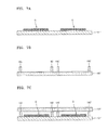
- FIGS. 7A to 7F are views sequentially illustrating a method of manufacturing a display apparatus according to an embodiment of the present invention.
- FIGS. 7A to 7F illustrate a method of manufacturing the display apparatus 100 of FIG. 1 .
- a mother substrate 101 ′ is prepared.
- the mother substrate 101 ′ may be formed of one of glass, plastic, and other suitable materials, and more particularly, may be formed of transparent glass.
- One or more display units D are formed on the mother substrate 101 ′. In FIG. 7A , two display units D are formed. However, the number of display units D on the mother substrate 101 ′ is not limited thereto.
- a preliminary sealing unit 180 ′ is formed on a mother encapsulation substrate 191 ′.
- the preliminary sealing unit 180 ′ may be formed corresponding to locations surrounding the display units D of the mother substrate 101 ′ while being formed on the mother encapsulation substrate 191 ′.
- the preliminary sealing unit 180 ′ is formed on the mother encapsulation substrate 191 ′ as a paste.
- the preliminary sealing unit 180 ′ is a paste containing glass frit and a filler. Since the glass frit and the filler are the same as those described above, a detailed description thereof will not be repeated here.
- the preliminary sealing unit 180 ′ may be formed on one surface of the mother substrate 101 ′ to surround the display unit D.
- the preliminary sealing unit 180 ′ having the form of the paste will be described in more detail as follows. Powder containing the glass frit and powder containing the filler are prepared. Also, a binder and other solvents are added to the powders, thereby preparing the paste. Then, the paste is formed on the mother encapsulation substrate 191 ′ in a desired shape, thereby forming the preliminary sealing unit 180 ′. In this case, the preliminary sealing unit 180 ′ may be formed on the mother encapsulation substrate 191 ′ in the desired shape by using a screen printing method.
- the preliminary sealing unit 180 ′ having the form of the paste is sintered and dried to maintain the shape of the preliminary sealing unit 180 ′.
- the mother encapsulation substrate 191 ′ is disposed to face (to be opposite to) the mother substrate 101 ′, in which the mother encapsulation substrate 191 ′ is arranged with respect to the mother substrate 101 ′ to allow the preliminary sealing unit 180 ′ to be disposed to surround the display units D.
- a laser beam LB is emitted onto a top of the mother encapsulation substrate 191 ′.
- the laser beam LB is emitted onto a position to correspond to the preliminary sealing unit 180 ′.
- the preliminary sealing unit 180 ′ is melted and cured in such a way that the mother substrate 101 ′ and the mother encapsulation substrate 191 ′ are bonded to each other.
- the laser beam LB has a wavelength from about 700 to about 900 nanometers.
- the laser beam LB may have a wavelength of about 800 nanometers, and more particularly, may have a wavelength of 810 nanometers.
- the absorptance of the preliminary sealing unit 180 ′ for the laser beam LB is low while emitting the laser beam LB, a part of the preliminary sealing unit 180 ′ is not melted.
- a less melted area of the preliminary sealing unit 180 ′ notably deteriorates bonding properties between the mother substrate 101 ′ and the mother encapsulation substrate 191 ′ and a space between the mother substrate 101 ′ and the mother encapsulation substrate 191 ′, formed as the preliminary sealing unit 180 ′, is not perfectly sealed, and thus, external gases, humidity, and other foreign substances may easily damage the display unit D.
- the preliminary sealing unit 180 ′ contains the glass frit and the filler and, as described above, the laser beam absorptance of the preliminary sealing unit 180 ′ is notably improved due to the filler, and thus, the preliminary sealing unit 180 ′ is effectively melted to effectively bond the mother substrate 101 ′ and the mother encapsulation substrate 191 ′ to each other.
- the preliminary sealing unit 180 ′ is melted in a very short amount of time.
- damage to the preliminary sealing unit 180 ′, the mother encapsulation substrate 191 ′, and the display unit D may be effectively prevented.
- the preliminary sealing unit 180 ′ is changed into the sealing unit 180 bonding the mother substrate 101 ′ and the mother encapsulation substrate 191 ′ to each other.
- the mother substrate 101 ′ and the mother encapsulation substrate 191 ′ are cut off based on a cutting-plane line CL. As a result thereof, finally, the display apparatus 100 is manufactured as shown in FIG. 7F .
Landscapes
- Engineering & Computer Science (AREA)
- Physics & Mathematics (AREA)
- Optics & Photonics (AREA)
- Manufacturing & Machinery (AREA)
- Microelectronics & Electronic Packaging (AREA)
- General Physics & Mathematics (AREA)
- Theoretical Computer Science (AREA)
- Electroluminescent Light Sources (AREA)
Abstract
Description
Claims (19)
Applications Claiming Priority (2)
| Application Number | Priority Date | Filing Date | Title |
|---|---|---|---|
| KR1020130054643A KR20140134565A (en) | 2013-05-14 | 2013-05-14 | Display apparatus and method for manufacturing the same |
| KR10-2013-0054643 | 2013-05-14 |
Publications (2)
| Publication Number | Publication Date |
|---|---|
| US20140339510A1 US20140339510A1 (en) | 2014-11-20 |
| US9276232B2 true US9276232B2 (en) | 2016-03-01 |
Family
ID=51883128
Family Applications (1)
| Application Number | Title | Priority Date | Filing Date |
|---|---|---|---|
| US14/024,494 Expired - Fee Related US9276232B2 (en) | 2013-05-14 | 2013-09-11 | Display apparatus and method of manufacturing the same |
Country Status (4)
| Country | Link |
|---|---|
| US (1) | US9276232B2 (en) |
| KR (1) | KR20140134565A (en) |
| CN (1) | CN104157667A (en) |
| TW (1) | TW201444078A (en) |
Families Citing this family (6)
| Publication number | Priority date | Publication date | Assignee | Title |
|---|---|---|---|---|
| KR102264651B1 (en) * | 2015-02-03 | 2021-06-15 | 삼성디스플레이 주식회사 | Display apparatus and method for manufacturing the same |
| KR102349282B1 (en) | 2015-03-27 | 2022-01-11 | 삼성디스플레이 주식회사 | Display apparatus and method for manufacturing the same |
| CN107204405A (en) * | 2016-03-18 | 2017-09-26 | 上海和辉光电有限公司 | A kind of organic electroluminescence display panel and its method for packing |
| CN107611282B (en) * | 2017-09-27 | 2019-01-22 | 京东方科技集团股份有限公司 | Package structure and display device |
| KR102587002B1 (en) * | 2017-11-15 | 2023-10-10 | 삼성디스플레이 주식회사 | Display device and method for manufacturing the display device |
| KR102809214B1 (en) * | 2020-05-08 | 2025-05-19 | 삼성디스플레이 주식회사 | Display device and manufacturing method of display device |
Citations (19)
| Publication number | Priority date | Publication date | Assignee | Title |
|---|---|---|---|---|
| US4892847A (en) | 1988-06-13 | 1990-01-09 | Ciba-Geigy Corporation | Lead-free glass frit compositions |
| US5250112A (en) * | 1991-12-05 | 1993-10-05 | Bayer Aktiengesellschaft | Spinel black pigments based on copper-chromium-manganese mixed oxides, a process for their preparation and their use |
| WO2004000745A1 (en) | 2002-06-20 | 2003-12-31 | Koninklijke Philips Electronics N.V. | Glass frit and method for sealing glass surfaces together |
| KR20050016578A (en) | 2002-06-20 | 2005-02-21 | 코닌클리케 필립스 일렉트로닉스 엔.브이. | Glass frit and method for sealing glass surfaces together |
| KR20080016457A (en) | 2006-08-18 | 2008-02-21 | 코닝 인코포레이티드 | Borosilicate glass frit for hermetic sealing of light emitting device displays |
| US20080106194A1 (en) | 2006-11-07 | 2008-05-08 | Stephan Lvovich Logunov | Seal for light emitting display device, method, and apparatus |
| KR20080046401A (en) | 2006-11-22 | 2008-05-27 | 엘지디스플레이 주식회사 | Organic electroluminescent device and manufacturing method thereof |
| KR20090041867A (en) | 2007-10-25 | 2009-04-29 | (주)세라 | Lead-free frit compositions for sealing flat panel displays |
| US20090247385A1 (en) * | 2008-03-28 | 2009-10-01 | Asahi Glass Company, Limited | Frit |
| US7619031B2 (en) * | 2002-08-07 | 2009-11-17 | Techno Polymer Co., Ltd. | Low heat storing thermoplastic resin composition and molding thereof |
| KR20090129822A (en) | 2008-06-13 | 2009-12-17 | (주)세라 | Frit composition for sealing flat panel display panels |
| KR100943187B1 (en) | 2008-05-20 | 2010-02-19 | 삼성모바일디스플레이주식회사 | OLED display and manufacturing method thereof |
| KR20100058335A (en) | 2008-11-24 | 2010-06-03 | 신세라믹 주식회사 | Lead-free glass frit composition for use in sealing |
| KR20100129644A (en) | 2009-06-01 | 2010-12-09 | (주) 센불 | Slurry composition for sealing element of flat panel display panel and sealing element manufactured using same |
| US20110309339A1 (en) * | 2010-06-17 | 2011-12-22 | Samsung Mobile Display Co., Ltd. | Organic light-emitting display device and method of manufacturing the same |
| US20110310465A1 (en) * | 2010-06-18 | 2011-12-22 | Sony Corporation | Electrophoretic device, display, and electronic apparatus |
| US20120321902A1 (en) | 2010-03-05 | 2012-12-20 | Yoshihiro Kohara | Lead-free glass material for organic-el sealing, organic el display formed using the same |
| US20130056710A1 (en) | 2011-09-06 | 2013-03-07 | Jae-hwan Oh | Organic light-emitting display apparatus and method of manufacturing the same |
| US20130174608A1 (en) * | 2010-06-14 | 2013-07-11 | Asahi Glass Company, Limited | Sealing material paste and process for producing electronic device employing the same |
Family Cites Families (2)
| Publication number | Priority date | Publication date | Assignee | Title |
|---|---|---|---|---|
| EP2351717A4 (en) * | 2008-11-26 | 2012-04-25 | Asahi Glass Co Ltd | GLASS MEMBER HAVING A SEAL / LINK MATERIAL LAYER, ELECTRONIC DEVICE USING THE SAME, AND METHOD FOR MANUFACTURING THE SAME |
| WO2011130632A1 (en) * | 2010-04-15 | 2011-10-20 | Ferro Corporation | Low-melting lead-free bismuth sealing glasses |
-
2013
- 2013-05-14 KR KR1020130054643A patent/KR20140134565A/en not_active Withdrawn
- 2013-09-11 US US14/024,494 patent/US9276232B2/en not_active Expired - Fee Related
-
2014
- 2014-01-09 TW TW103100800A patent/TW201444078A/en unknown
- 2014-02-07 CN CN201410045154.2A patent/CN104157667A/en active Pending
Patent Citations (24)
| Publication number | Priority date | Publication date | Assignee | Title |
|---|---|---|---|---|
| KR900000306A (en) | 1988-06-13 | 1990-01-30 | 베르너 발데크 | Lead-free glass frit compositions |
| US4892847A (en) | 1988-06-13 | 1990-01-09 | Ciba-Geigy Corporation | Lead-free glass frit compositions |
| US5250112A (en) * | 1991-12-05 | 1993-10-05 | Bayer Aktiengesellschaft | Spinel black pigments based on copper-chromium-manganese mixed oxides, a process for their preparation and their use |
| WO2004000745A1 (en) | 2002-06-20 | 2003-12-31 | Koninklijke Philips Electronics N.V. | Glass frit and method for sealing glass surfaces together |
| KR20050016578A (en) | 2002-06-20 | 2005-02-21 | 코닌클리케 필립스 일렉트로닉스 엔.브이. | Glass frit and method for sealing glass surfaces together |
| US7619031B2 (en) * | 2002-08-07 | 2009-11-17 | Techno Polymer Co., Ltd. | Low heat storing thermoplastic resin composition and molding thereof |
| US20080124558A1 (en) * | 2006-08-18 | 2008-05-29 | Heather Debra Boek | Boro-silicate glass frits for hermetic sealing of light emitting device displays |
| KR20080016457A (en) | 2006-08-18 | 2008-02-21 | 코닝 인코포레이티드 | Borosilicate glass frit for hermetic sealing of light emitting device displays |
| US20080106194A1 (en) | 2006-11-07 | 2008-05-08 | Stephan Lvovich Logunov | Seal for light emitting display device, method, and apparatus |
| KR20080041558A (en) | 2006-11-07 | 2008-05-13 | 코닝 인코포레이티드 | Bags, methods and apparatus for light emitting display devices |
| KR20080046401A (en) | 2006-11-22 | 2008-05-27 | 엘지디스플레이 주식회사 | Organic electroluminescent device and manufacturing method thereof |
| KR20090041867A (en) | 2007-10-25 | 2009-04-29 | (주)세라 | Lead-free frit compositions for sealing flat panel displays |
| US20090247385A1 (en) * | 2008-03-28 | 2009-10-01 | Asahi Glass Company, Limited | Frit |
| KR100943187B1 (en) | 2008-05-20 | 2010-02-19 | 삼성모바일디스플레이주식회사 | OLED display and manufacturing method thereof |
| KR20090129822A (en) | 2008-06-13 | 2009-12-17 | (주)세라 | Frit composition for sealing flat panel display panels |
| KR20100058335A (en) | 2008-11-24 | 2010-06-03 | 신세라믹 주식회사 | Lead-free glass frit composition for use in sealing |
| KR20100129644A (en) | 2009-06-01 | 2010-12-09 | (주) 센불 | Slurry composition for sealing element of flat panel display panel and sealing element manufactured using same |
| US20120321902A1 (en) | 2010-03-05 | 2012-12-20 | Yoshihiro Kohara | Lead-free glass material for organic-el sealing, organic el display formed using the same |
| US20130174608A1 (en) * | 2010-06-14 | 2013-07-11 | Asahi Glass Company, Limited | Sealing material paste and process for producing electronic device employing the same |
| US20110309339A1 (en) * | 2010-06-17 | 2011-12-22 | Samsung Mobile Display Co., Ltd. | Organic light-emitting display device and method of manufacturing the same |
| KR20110137561A (en) | 2010-06-17 | 2011-12-23 | 삼성모바일디스플레이주식회사 | Organic light emitting display device and manufacturing method thereof |
| US20110310465A1 (en) * | 2010-06-18 | 2011-12-22 | Sony Corporation | Electrophoretic device, display, and electronic apparatus |
| US20130056710A1 (en) | 2011-09-06 | 2013-03-07 | Jae-hwan Oh | Organic light-emitting display apparatus and method of manufacturing the same |
| KR20130026807A (en) | 2011-09-06 | 2013-03-14 | 삼성디스플레이 주식회사 | Organic light emitting display apparatus and manufacturing method thereof |
Also Published As
| Publication number | Publication date |
|---|---|
| KR20140134565A (en) | 2014-11-24 |
| US20140339510A1 (en) | 2014-11-20 |
| TW201444078A (en) | 2014-11-16 |
| CN104157667A (en) | 2014-11-19 |
Similar Documents
| Publication | Publication Date | Title |
|---|---|---|
| TWI715561B (en) | Organic light-emitting display apparatus | |
| US7841919B2 (en) | Method of sealing an organic light emitting display using closed loop pattern of frit paste composition | |
| KR102082780B1 (en) | Organic light emitting display apparatus and method of manufacturing thereof | |
| US10944071B2 (en) | Organic light-emitting display apparatus and method of manufacturing the same | |
| KR102160813B1 (en) | Organic light emitting display and fabrication method for the same | |
| US8299705B2 (en) | Organic light emitting display device and manufacturing method thereof | |
| US9276232B2 (en) | Display apparatus and method of manufacturing the same | |
| US9178180B2 (en) | Display device and electronic apparatus | |
| US8674601B2 (en) | Flat panel display apparatus having sealing member partially overlapping outermost pixels and method of manufacturing the same | |
| US20150021568A1 (en) | Organic light emitting display apparatus and method of manufacturing the same | |
| JP2022079735A (en) | How to form a glass layer | |
| CN101009311A (en) | Organic light emitting display and method of fabricating the same | |
| US8288944B2 (en) | Organic light-emitting display apparatus sealed with a sealant containing a filler | |
| US9748515B2 (en) | Organic light-emitting diode display and method of manufacturing the same including a sealant with a plurality of openings and islands formed within the openings | |
| KR20140089856A (en) | Organic light emitting display apparatus and method of manufacturing thereof | |
| US20090206738A1 (en) | Organic light-emitting diode display device and method of manufacturing the same | |
| KR101193199B1 (en) | Organic light emitting display apparatus | |
| KR101605008B1 (en) | Fabrication method for organic light emitting diodes device | |
| CN114242917A (en) | Rigid display screen packaging method | |
| KR20160076002A (en) | Display device and manufacturing method thereof | |
| JP2012204076A (en) | Display device and method for manufacturing the same |
Legal Events
| Date | Code | Title | Description |
|---|---|---|---|
| AS | Assignment |
Owner name: SAMSUNG DISPLAY CO., LTD, KOREA, REPUBLIC OF Free format text: ASSIGNMENT OF ASSIGNORS INTEREST;ASSIGNORS:LEE, JAE-MAN;YOO, SEUNG-JOON;SHIN, JAE-WOOK;REEL/FRAME:031187/0587 Effective date: 20130813 |
|
| ZAAA | Notice of allowance and fees due |
Free format text: ORIGINAL CODE: NOA |
|
| ZAAB | Notice of allowance mailed |
Free format text: ORIGINAL CODE: MN/=. |
|
| FEPP | Fee payment procedure |
Free format text: PAYOR NUMBER ASSIGNED (ORIGINAL EVENT CODE: ASPN); ENTITY STATUS OF PATENT OWNER: LARGE ENTITY |
|
| STCF | Information on status: patent grant |
Free format text: PATENTED CASE |
|
| MAFP | Maintenance fee payment |
Free format text: PAYMENT OF MAINTENANCE FEE, 4TH YEAR, LARGE ENTITY (ORIGINAL EVENT CODE: M1551); ENTITY STATUS OF PATENT OWNER: LARGE ENTITY Year of fee payment: 4 |
|
| FEPP | Fee payment procedure |
Free format text: MAINTENANCE FEE REMINDER MAILED (ORIGINAL EVENT CODE: REM.); ENTITY STATUS OF PATENT OWNER: LARGE ENTITY |
|
| LAPS | Lapse for failure to pay maintenance fees |
Free format text: PATENT EXPIRED FOR FAILURE TO PAY MAINTENANCE FEES (ORIGINAL EVENT CODE: EXP.); ENTITY STATUS OF PATENT OWNER: LARGE ENTITY |
|
| STCH | Information on status: patent discontinuation |
Free format text: PATENT EXPIRED DUE TO NONPAYMENT OF MAINTENANCE FEES UNDER 37 CFR 1.362 |
|
| FP | Lapsed due to failure to pay maintenance fee |
Effective date: 20240301 |