US9256138B2 - Method for measuring distortion of projection objective - Google Patents
Method for measuring distortion of projection objective Download PDFInfo
- Publication number
- US9256138B2 US9256138B2 US14/002,917 US201214002917A US9256138B2 US 9256138 B2 US9256138 B2 US 9256138B2 US 201214002917 A US201214002917 A US 201214002917A US 9256138 B2 US9256138 B2 US 9256138B2
- Authority
- US
- United States
- Prior art keywords
- stage
- stepping
- marks
- reticle
- exposure
- Prior art date
- Legal status (The legal status is an assumption and is not a legal conclusion. Google has not performed a legal analysis and makes no representation as to the accuracy of the status listed.)
- Active, expires
Links
Images


Classifications
-
- G—PHYSICS
- G03—PHOTOGRAPHY; CINEMATOGRAPHY; ANALOGOUS TECHNIQUES USING WAVES OTHER THAN OPTICAL WAVES; ELECTROGRAPHY; HOLOGRAPHY
- G03F—PHOTOMECHANICAL PRODUCTION OF TEXTURED OR PATTERNED SURFACES, e.g. FOR PRINTING, FOR PROCESSING OF SEMICONDUCTOR DEVICES; MATERIALS THEREFOR; ORIGINALS THEREFOR; APPARATUS SPECIALLY ADAPTED THEREFOR
- G03F7/00—Photomechanical, e.g. photolithographic, production of textured or patterned surfaces, e.g. printing surfaces; Materials therefor, e.g. comprising photoresists; Apparatus specially adapted therefor
- G03F7/70—Microphotolithographic exposure; Apparatus therefor
- G03F7/70483—Information management; Active and passive control; Testing; Wafer monitoring, e.g. pattern monitoring
- G03F7/70591—Testing optical components
- G03F7/706—Aberration measurement
-
- G—PHYSICS
- G03—PHOTOGRAPHY; CINEMATOGRAPHY; ANALOGOUS TECHNIQUES USING WAVES OTHER THAN OPTICAL WAVES; ELECTROGRAPHY; HOLOGRAPHY
- G03F—PHOTOMECHANICAL PRODUCTION OF TEXTURED OR PATTERNED SURFACES, e.g. FOR PRINTING, FOR PROCESSING OF SEMICONDUCTOR DEVICES; MATERIALS THEREFOR; ORIGINALS THEREFOR; APPARATUS SPECIALLY ADAPTED THEREFOR
- G03F1/00—Originals for photomechanical production of textured or patterned surfaces, e.g., masks, photo-masks, reticles; Mask blanks or pellicles therefor; Containers specially adapted therefor; Preparation thereof
- G03F1/38—Masks having auxiliary features, e.g. special coatings or marks for alignment or testing; Preparation thereof
- G03F1/44—Testing or measuring features, e.g. grid patterns, focus monitors, sawtooth scales or notched scales
-
- G—PHYSICS
- G03—PHOTOGRAPHY; CINEMATOGRAPHY; ANALOGOUS TECHNIQUES USING WAVES OTHER THAN OPTICAL WAVES; ELECTROGRAPHY; HOLOGRAPHY
- G03F—PHOTOMECHANICAL PRODUCTION OF TEXTURED OR PATTERNED SURFACES, e.g. FOR PRINTING, FOR PROCESSING OF SEMICONDUCTOR DEVICES; MATERIALS THEREFOR; ORIGINALS THEREFOR; APPARATUS SPECIALLY ADAPTED THEREFOR
- G03F7/00—Photomechanical, e.g. photolithographic, production of textured or patterned surfaces, e.g. printing surfaces; Materials therefor, e.g. comprising photoresists; Apparatus specially adapted therefor
- G03F7/70—Microphotolithographic exposure; Apparatus therefor
- G03F7/70483—Information management; Active and passive control; Testing; Wafer monitoring, e.g. pattern monitoring
- G03F7/70605—Workpiece metrology
- G03F7/70616—Monitoring the printed patterns
- G03F7/70633—Overlay, i.e. relative alignment between patterns printed by separate exposures in different layers, or in the same layer in multiple exposures or stitching
-
- G—PHYSICS
- G03—PHOTOGRAPHY; CINEMATOGRAPHY; ANALOGOUS TECHNIQUES USING WAVES OTHER THAN OPTICAL WAVES; ELECTROGRAPHY; HOLOGRAPHY
- G03F—PHOTOMECHANICAL PRODUCTION OF TEXTURED OR PATTERNED SURFACES, e.g. FOR PRINTING, FOR PROCESSING OF SEMICONDUCTOR DEVICES; MATERIALS THEREFOR; ORIGINALS THEREFOR; APPARATUS SPECIALLY ADAPTED THEREFOR
- G03F7/00—Photomechanical, e.g. photolithographic, production of textured or patterned surfaces, e.g. printing surfaces; Materials therefor, e.g. comprising photoresists; Apparatus specially adapted therefor
- G03F7/70—Microphotolithographic exposure; Apparatus therefor
- G03F7/70691—Handling of masks or workpieces
- G03F7/70716—Stages
- G03F7/70725—Stages control
Definitions
- the present invention relates in general to the manufacturing of integrated circuits, and more particularly, to a method for measuring distortion of a projection objective used in a lithography machine:
- Lithography also known as photolithography
- This technology employs a lithographic system to expose and transfer a reticle pattern onto a photoresist.
- the lithographic system ultimately determines the critical dimension of an integrated circuit being manufactured, its precision is of great significance to a lithography process.
- a silicon wafer coated with photoresist is sucked on a wafer chuck, and its top surface shall be set at an optimum image plane height to achieve the best imaging result.
- a lithography machine is a device used in the manufacturing of integrated circuits.
- lithography apparatuses for integrated circuits, liquid crystal display (LCD) panels, photomasks, micro-electro-mechanical systems (MEMSs)/micro-opto-mechanical systems (MOMSs), advanced packaging, printed circuit boards, and also in PCB processing apparatuses, etc.
- LCD liquid crystal display
- MEMSs micro-electro-mechanical systems
- MOMSs micro-opto-mechanical systems
- PCB processing apparatuses etc.
- the first method is to measure the image quality of a projection objective by using reticle alignment sensors of a lithography machine.
- reticle alignment sensors of a lithography machine Such method is disclosed in, for example, U.S. Pat. No. 7,333,175 and WO94/01808.
- this method as an optical path passes through the objective during the alignment of the reticle, distortion of the objective can be reflected by the alignment results.
- drawbacks of this method include: firstly, both interferometer and reticle alignment system of the lithography machine are required to have a high performance as the precision of the objective distortion measurement is highly dependent on the repeatability of the measurement of reticle alignment marks; secondly, the method is relied on specific reticle alignment approaches.
- the manufacturing and processing of an alignment mark grating is highly complicated, and hence will lead to a high cost in the fabrication of a reticle having a high-precision alignment mark array.
- high-order distortion itself will affect the reticle alignment sensors during the detection of alignment positions, and therefore limits the applicability of this method.
- the method is only suited for measuring low-order distortions but not high-order distortions of an objective.
- the second method is to measure the distortions of a projection objective by using image quality sensors.
- image quality sensors Such method is disclosed in, for example, U.S. Pat. Nos. 0,136,070, 0,144,043, 0,264,827 and 6,650,399.
- Such sensors with high precision, are specially designed for the measurement of objective image quality, including high-order distortions and performance of the objective.
- these sensors typically have a delicate and complex structure, and in particular, optical elements of these sensors require extremely expensive manufacturing technology.
- the sensors must cooperate with a high-performance lithography machine to play the best performance in objective distortion measurement. For these reasons, except some most high-end lithography machines, currently used common ones cannot afford to be equipped with such sensors, and hence the method has a low adaptability for lithography machines.
- An objective of the present invention is to provide a method for measuring distortion of a projection objective, which can achieve a high measurement precision and a high adaptability.
- the present invention provides a method for measuring distortion of a projection objective, including:
- a reticle on a reticle stage and disposing a substrate on a workpiece stage, the reticle having a plurality of marks formed thereon;
- performing a stepping and exposing process of the reticle stage including: moving the substrate into an exposure field of the projection objective; performing a first exposure process to form on the substrate a first pattern of the plurality of marks corresponding to the current exposure field; keeping the workpiece stage unmoved and stepping the reticle stage by a first distance, and then performing a second exposure process to form on the substrate a second pattern of the plurality of marks corresponding to the current exposure field; obtaining a first positional deviation between the first pattern and the second pattern;
- performing a stepping and exposing process of the workpiece stage including: moving the substrate into an exposure field of the projection objective; performing a first exposure process to form on the substrate a third pattern of the plurality of marks corresponding to the current exposure field; keeping the reticle stage unmoved and stepping the workpiece stage by a second distance, and then performing a second exposure process to form on the substrate a fourth pattern of the plurality of marks corresponding to the current exposure field; obtaining a second positional deviation between the third pattern and the fourth pattern;
- the substrate is disposed on the workpiece stage at a position aligned with a center of the projection objective.
- the stepping and exposing process of the reticle stage is performed prior to the stepping and exposing process of the workpiece stage, or the stepping and exposing process of the workpiece stage is performed prior to the stepping and exposing process of the reticle stage.
- performing the stepping and exposing process of the reticle stage further includes optimizing an exposure path prior to moving the substrate into an exposure field of the projection objective; and performing the stepping and exposing process of the workpiece stage further includes optimizing an exposure path prior to moving the substrate into an exposure field of the projection objective.
- each of the plurality of marks includes two portions arranged in parallel to each other.
- each of the plurality of marks is an overlay mark.
- the reticle stage is stepped by a first distance in a direction along a line connecting centers of the two portions of any of the plurality of marks, and wherein the workpiece stage is stepped by a second distance in a direction along a line connecting centers of the two portions of any of the plurality of marks.
- the first distance is D*Nom_mag, where D is a distance between the centers of the two portions of each of the plurality of marks, and Nom_mag is a nominal magnification of the projection objective.
- the second distance is D, where D is a distance between the centers of the two portions of each of the plurality of marks.
- the motional error of the reticle stage and/or the workpiece stage includes a translational error and a rotational error of the reticle stage and/or the workpiece stage.
- the present invention further provides a method for measuring distortion of a projection objective, including:
- a reticle on a reticle stage and disposing a substrate on a workpiece stage, the reticle having a plurality of marks formed thereon;
- performing a stepping and exposing process of the reticle stage including:
- performing a stepping and exposing process of the workpiece stage including:
- the methods of the present invention have low dependency on the type of the reticle marks.
- the methods may employ common overlay marks used in combination with an overlay reticle or may employ some other specially designed marks.
- the process of objective distortion measurement is performed in a same way as normal operation of the lithography machine, it can well represent distortion in image quality induced during the exposure process of the lithography machine, and thereby may enhance objectivity and accuracy of the measurement results.
- the methods are implemented by directly performing exposures, which enables the measurement accuracy to be directly determined by the image quality factors of the projection objective, thus imposing few requirements on external devices or configurations of the lithography machine and giving the methods suitability for any high-end or low-end lithography machines.
- the methods of the present invention have no limitations to alignment approaches of the lithography machine, thereby results in the reduction of manufacturing cost of the lithography machine and an increase of adaptability of the methods.
- FIG. 1 is a schematic diagram illustrating main components of a lithography machine employed in a method for measuring projection objective distortion in accordance with embodiments of the present invention.
- FIG. 2 is a schematic illustration of a mark used in a method for measuring projection objective distortion in accordance with a preferred embodiment of the present invention.
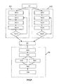
- FIG. 3 is a flow chart depicting a method for measuring projection objective distortion in accordance with embodiments of the present invention.
- FIGS. 4A to 4C are schematic illustrations of patterns formed on silicon wafers after the mark of FIG. 2 is exposed.
- FIG. 5 is a detailed flow chart depicting a method for measuring projection objective distortion in accordance with a preferred embodiment of the present invention.
- the present invention is based on a core concept of measuring projection objective distortion by exposures, and more specifically, is based on the main principle as follows: by performing a stepping and exposing process of the workpiece stage and performing a stepping and exposing process of the reticle stage respectively, exposed patterns corresponding to these two processes can be obtained on the substrate, and positional deviations of the exposed patterns corresponding to each of these two processes can be calculated.
- the exposure positions will correspond to different positions in the projection objective and hence a distortion of the projection objective will be contained in the positional deviation of the corresponding patterns; and conversely, when the reticle stage is moved while keeping the workpiece stage unmoved, the exposure positions will be an identical position in the projection objective and hence no distortion of the projection objective will be contained in the positional deviation of the corresponding patterns.
- distortion of the projection objective can be derived from statistical analysis of the positional deviations of the patterns generated by these two different types of stepping and exposing processes.
- FIG. 1 is a schematic diagram illustrating main components of a lithography machine employed in a projection objective distortion measurement method embodying the present invention.
- main components include: a reticle 5 clamped or fixed on a reticle stage 6 , the reticle stage 6 carrying the reticle 5 to move in multiple degrees of freedom, the reticle 5 having a plurality of marks evenly distributed thereon in an exposure area; a substrate 2 (e.g., silicon wafer, glass substrate, sapphire substrate, etc.), sucked on a workpiece stage 3 and able to move together with the workpiece stage 3 ; and a projection objective 7 for imaging the plurality of marks of the reticle 5 onto the substrate 2 .
- a substrate 2 e.g., silicon wafer, glass substrate, sapphire substrate, etc.
- the method of the present invention has high adaptability and does not require any extra component which is special and expensive.
- FIG. 2 is a schematic illustration of one of the plurality of marks used in a projection objective distortion measurement method in a preferred embodiment of the present invention.
- the mark 1 is a commonly used overlay mark comprising two portions, wherein a center of the first portion 101 is a distance D from a center of the second portion 102 .
- the mark 1 may either be used in combination with an overlay reticle or be designed as some other special mark.
- the method of the present invention has no specific requirements on the mark 1 , and thus has little dependency on the mark 1 .
- the first portion 101 is consisted of four stripes having identical shape and size. In addition, the four stripes are joined together at their ends and thereby enclose a large square area.
- the second portion 102 is arranged in parallel to the first portion 101 and has a small square shape which can fit inside the large square area enclosed by the four stripes of the first portion 101 .
- the present invention is not limited to the mark 1 shown in FIG. 2 .
- the present invention may employ any other commonly used overlay marks or any special marks that enable overlay error measurement.
- a method for measuring distortion of a projection objective in accordance with an embodiment of the present invention will be specified and described below with reference to FIG. 3 , FIGS. 4A to 4C , and FIG. 5 .
- the method substantially includes four stages, wherein the first stage S 1 is a preparation stage; the second stage S 2 is an exposure stage; the third stage S 3 is a wafer processing stage; and the fourth stage S 4 is an objective distortion calculation stage.
- the second stage S 2 further includes two sub-stages, namely a stepping and exposing process of the reticle stage S 21 and a stepping and exposing process of the workpiece stage S 22 .
- the two sub-stages S 21 and S 22 may be performed one after another in either sequential order.
- the reticle 5 having a plurality of marks 1 formed thereon is placed on the reticle stage 6 and has a fixed relative position with respect to the reticle stage 6 .
- the plurality of marks 1 are uniformly and evenly distributed in an exposure area of the reticle 5 .
- the substrate 2 which is a silicon wafer 2 in this embodiment, is placed on the workpiece stage 3 .
- at least two pieces of silicon wafers 2 are needed, one of which is a reference wafer having an alignment mark formed thereon for reticle alignment and wafer alignment.
- the silicon wafer 2 is preferably placed at a position aligned with a center of the projection objective 7 , such that the area to be exposed substantially coincides with an area of the projection objective 7 to be measured.
- the purpose of the preparation stage S 1 is for setting the components of the lithography machine in place.
- the second stage S 2 is an exposure stage which further includes two sub-stages, namely a stepping and exposing process of the reticle stage S 21 and a stepping and exposing process of the workpiece stage S 22 .
- FIG. 5 depicts details of the exposure stage S 2 .
- the stepping and exposing process of the reticle stage S 21 includes the following steps:
- step S 211 an exposure path is optimized.
- step S 212 an exposure system is adjusted and controlled to make sure that the lithography machine meets the exposure requirements.
- a first exposure process is performed on a first silicon wafer 2 .
- the first exposure process mainly includes: moving the workpiece stage 3 to position the silicon wafer 2 sucked thereon in a first exposure field; and exposing the plurality of reticle marks on the first silicon wafer 2 .
- a plurality of first patterns 11 corresponding to the plurality of reticle marks are formed on the silicon wafer.
- FIG. 4A shows an example of one of the plurality of first patterns 11 .
- a positional coordinate (Wx11, Wy11) of each first pattern 11 in the coordinate system of the silicon wafer 2 and a positional coordinate (Fx11, Fy11) of each first pattern 11 in the coordinate system of the first exposure field may be easily measured using any appropriate existing method in a subsequent stage.
- the coordinate (Wx11, Wy11) may be defined as a coordinate of a center of the first portion 101 of the first pattern 11 , or a coordinate of a center of the second portion 102 of the first pattern 11 with respect to a center of the silicon wafer 2 .
- the coordinate (Fx11, Fy11) may be defined as a coordinate of a center of the entire first pattern 11 , or a coordinate of the center of any one of the first and second portions 101 , 102 of the first pattern 11 with respect to a center of the current exposure field (i.e., the first exposure field).
- ‘11’ in (Wx11, Wy11) and (Fx11, Fy11) indicates that the coordinates are corresponding to the ‘1’st exposure field and the ‘1’st exposure.
- step S 214 a second exposure process is performed on the first silicon wafer 2 .
- L D*Nom_mag
- Nom_mag is a nominal magnification of the objective 7 .
- a second exposure in the first exposure field and after which a plurality of second patterns 12 corresponding to the plurality of reticle marks 1 are formed on the silicon wafer 2 .
- One of the plurality of second patterns 12 is exemplarily illustrated as the grey shadings in FIG. 4C .
- a positional coordinate (Wx12, Wy12) of each second pattern 12 in the coordinate system of the silicon wafer 2 , a positional coordinate (Fx12, Fy12) of each second pattern 12 in the coordinate system of the first exposure field and a positional deviation (Ex1, Ey1) between each pair of first and second patterns 11 and 12 may be easily measured using an appropriate existing method in a subsequent stage.
- ‘12’ in (Wx12, Wy12) and (Fx12, Fy12) indicates that the coordinates are corresponding to the ‘1’st exposure field and the ‘2’nd exposure.
- the positional deviation (Ex1, Ey1) is defined as a distance between a center of the second portion 102 of one of the first patterns 11 and a center of a first portion 101 of a corresponding one of the second patterns 12 obtained in the first exposure field, namely, an overlay error between each pair of first and second patterns 11 and 12 formed by the respective two exposures in the first exposure field.
- the overlay errors may be read using an existing overlay tool or any other relevant device, detailed description of which is omitted herein.
- the positional deviation (Ex1, Ey1) between any pair of the two exposure patterns 11 and 12 of the first exposure field shall not contain distortion of the projection objective 7 .
- What shall be mainly contained in the positional deviation (Ex1, Ey1) include translational and rotational errors introduced by the movement of the reticle stage 6 and/or the workpiece stage 3 , and manufacturing tolerance error of the reticle 5 .
- step S 215 is performed to move the workpiece stage 3 into a next exposure field (or a second exposure field) and carry out two exposures in the second exposure field in a similar manner as described in steps S 213 and S 214 .
- step S 215 includes: moving the workpiece stage 3 to position the silicon wafer 2 sucked thereon in the second exposure field; performing a first exposure to form a plurality of patterns on the silicon wafer 2 and the positional coordinates (Wx21, Wy21) and (Fx21, Fy21) of each pattern may be derived in a subsequent stage; next, fixing the workpiece stage 3 in its position and controlling the reticle stage 6 to step a distance L in the ⁇ Y direction; performing a second exposure to form another plurality of patterns of the reticle marks on the silicon wafer 2 and the positional coordinates (Wx22, Wy22) and (Fx22, Fy22) of each of the another plurality of patterns as well as a positional deviation (Ex2, Ey2) between each pair of the two patterns obtained by the respective two exposures in the second exposure field may be derived in a subsequent stage.
- the positional deviations (Ex2, Ey2) shall not include distortion of the projection objective.
- the workpiece stage 3 may be moved into a next exposure field and carry out two further exposures.
- the stepping and exposing process of the workpiece stage S 22 may be carried out in a similar way to the stepping and exposing process of the reticle stage S 21 , and it mainly differs from sub-stage S 21 in moving the workpiece stage 3 while keeping the reticle stage 6 unmoved.
- Sub-stage S 22 may include the steps described in detail below.
- step S 221 an exposure path is optimized.
- step S 222 an exposure system is adjusted and controlled to make sure that the lithography machine meets the exposure requirements.
- steps S 221 and S 222 are similar to steps S 211 and S 212 , reference can be made here to the above description of steps S 211 and S 212 .
- a first exposure process is performed on a second silicon wafer 2 .
- the first exposure process mainly includes: moving the workpiece stage 3 to position the silicon wafer 2 thereon in a first exposure field; and exposing the reticle marks on the second silicon wafer 2 .
- a plurality of patterns 13 corresponding to the plurality of reticle marks are formed on the silicon wafer.
- FIG. 4B shows an example of one of the plurality of patterns 13 .
- a positional coordinate (W′x11, W′y11) of each pattern 13 in the coordinate system of the second silicon wafer 2 and a positional coordinate (F′x11, F′y11) of each pattern 13 in the coordinate system of the first exposure field may be easily measured using an appropriate existing method in a subsequent stage.
- the coordinate (W′x11, W′y11) may be defined as a coordinate of a center of the first portion 101 of the pattern 13 , or a coordinate of a center of the second portion 102 of the pattern 13 with respect to a center of the second silicon wafer 2 .
- the coordinate (F′x11, F′y11) may be defined as a coordinate of a center of the entire pattern 13 , or a coordinate of the center of any one of the first and second portions 101 , 102 of the pattern 13 with respect to a center of the current exposure field (i.e., the first exposure field).
- step S 224 a second exposure process is performed on the second silicon wafer 2 .
- the reticle stage 6 is fixed in its position and the workpiece stage 3 is controlled to step a distance D in the +Y direction (or in ⁇ Y, +X, or ⁇ X directions according to the structure of the mark or the exposure path).
- the second exposure is also performed in the first exposure field, and after which a plurality of patterns 14 corresponding to the plurality of reticle marks are formed on the second silicon wafer 2 .
- One of the plurality of patterns 14 is exemplarily illustrated as the grey shadings in FIG. 4B .
- a positional coordinate (W′x12, W′y12) of each pattern 14 in the coordinate system of the second silicon wafer 2 , a positional coordinate (F′x12, F′y12) of each pattern 14 in the coordinate system of the first exposure field and a positional deviation (E′x1, E′y1) between each pair of patterns 13 and 14 may be easily measured using an appropriate existing method in a subsequent stage.
- the positional deviations (E′x1, E′y1) between the respective pairs of two exposure patterns 13 and 14 of the first exposure field shall contain distortion of the projection objective 7 in addition to translational and rotational errors introduced by the movement of the reticle stage 6 and/or the workpiece stage 3 as well as manufacturing tolerance error of the reticle 5 .
- an actual distance (see FIG. 4B ) between each pair of two patterns 13 and 14 formed on the second silicon wafer 2 after the two exposures has a great difference with the distance D.
- step S 225 the workpiece stage 3 is moved into a next exposure field (or a second exposure field), and further two exposures are performed in the second exposure field in a similar manner as described in steps S 223 and S 224 .
- step S 225 includes: moving the workpiece stage 3 to position the second silicon wafer 2 thereon in the second exposure field; performing a first exposure to form a plurality of patterns of the reticle marks on the second silicon wafer 2 and the positional coordinates (W′x21, W′y21) and (F′x21, F′y21) of each pattern may be derived in a subsequent stage; then, fixing the reticle stage 6 in its position and controlling the workpiece stage 3 to step a distance D in the +Y direction; performing a second exposure to form another plurality of patterns of the reticle marks on the second silicon wafer 2 and the positional coordinates (W′x22, W′y22) and (F′x22, F′y22) of each of the another plurality of patterns as well
- the positional deviations (E′x2, E′y2) shall include distortion of the projection objective.
- the workpiece stage 3 may be moved into a next exposure field and carry out two further exposures.
- the fourth stage S 4 is an objective distortion calculation stage. In this stage, deviations generated in the exposure processes are analyzed and the objective distortion is calculated based on the analysis results.
- FIG. 5 shows an embodiment of the fourth stage, which may include steps discussed below.
- step S 41 for each of the stepping and exposing process of the reticle stage S 21 and the stepping and exposing process of the workpiece stage S 22 , obtain a plurality of sets of positional deviations (Ex, Ey) corresponding to a plurality of exposure fields, wherein each set of positional deviations (Ex, Ey) is obtained from a plurality of pairs of patterns generated by the corresponding two exposures of the same exposure field.
- coordinates (Wx, Wy) and (Fx, Fy) of each exposed pattern namely each of the patterns formed on the silicon wafers, may be measured concurrently with the measurement of the deviations (Ex, Ey).
- definitions and measurement methods of the positional deviations (Ex, Ey) and the positional coordinates (Wx, Wy) and (Fx, Fy) have been described supra, description of them are omitted herein for simplicity.
- step S 42 fitting the translational errors (Tx, Ty) and rotational errors (Rx, Ry) of the reticle stage 6 and/or the workpiece stage 3 generated in the stepping and exposing process of the reticle stage S 21 and the stepping and exposing process of the workpiece stage S 22 , respectively so as to subtract these errors (Tx, Ty) and (Rx, Ry) from the positional deviations (Ex, Ey).
- Xslit and Yslit are sizes of a field of view (FOV) in the X and Y directions, respectively.
- the inter-field errors caused by the translation and rotation of the workpiece stage 3 and/or the reticle stage 6 can be removed from the positional deviations (Ex, Ey) of the respective pairs of patterns, and hence are not contained in the residuals (dx, dy) calculated.
- step S 43 obtain corrected deviations (dx1, dy1) of the respective pairs of patterns formed in the stepping and exposing process of the reticle stage S 21 by subtracting the translational errors (Tx, Ty) and rotational errors (Rx, Ry).
- the corrected deviations (dx1, dy1) of each exposure field are obtained by calculating the residuals (dx, dy) of the respective pairs of patterns of the same exposure field using the above Equation 1 and a fitting algorithm.
- step S 43 corresponds to sub-stage S 21 which is, as discussed above, the stepping and exposing process of the reticle stage
- step S 43 is able to subtract the errors of the projection objective caused by the distance D between the portions 101 and 102 of each mark 1 . Therefore, what is mainly contained in the corrected deviations (dx1, dy1) obtained after step S 43 is the manufacturing tolerance error of the reticle 5 .
- step S 44 obtain corrected deviations (dx2, dy2) of the respective pairs of patterns formed in the stepping and exposing process of the workpiece stage S 22 by subtracting the translational errors (Tx, Ty) and rotational errors (Rx, Ry).
- the corrected deviations (dx2, dy2) of each exposure field are obtained by calculating the residuals (dx, dy) of the respective pairs of patterns of the same exposure field using the above Equation 1 and a fitting algorithm.
- Step S 44 corresponds to sub-stage S 22 which is, as discussed above, the stepping and exposing process of the workpiece stage.
- each mark 1 itself has a certain size in both the X and Y directions, the two exposure positions of the same mark 1 in a corresponding exposure field will appear to be different imaging positions in the projection objective 7 , and thus the distortion of the projection objective 7 will be incorporated in the corresponding corrected deviations (dx2, dy2) as exposure position deviations.
- the manufacturing tolerance error of the reticle is offset, thereby enabling the values ( ⁇ x, ⁇ y) to exactly represent the overall objective distortion without being affect by the manufacturing tolerance error of the reticle.
Abstract
Description
Ex=Tx−Rx·Fy+dx
Ey=Ty+Ry·Fx+dy
Fx ε[−Xslit/2,Xslit/2], Fy ε[−Yslit/2,Yslit/2] (Equation 1)
Δx=dx 2 dx 1
Δy=dy 2 −dy 1 (Equation 2)
Δx=Tx+Mx·x−Rx·y+Txy·x·y+D2x·x 2+(D2x−Tyx)·y 2 +D3·x·r 2 D4x·x 2 ·r 2 +D4y·x·y·r 2 +D5·x·r 4
Δy=Ty+My·y+Ry·x+Tyx·y·x+D2y·y 2+(D2y−Txy)·x 2 +D3·y·r 2 +D4x·x·y·r 2 +D4y·y 2 ·r 2 +D5·y·r 4
x ε[−Xslit/2, Xslit/2],y ε[−Yslit/2, Yslit/2] (Equation 3)
Claims (20)
Applications Claiming Priority (4)
| Application Number | Priority Date | Filing Date | Title |
|---|---|---|---|
| CN201110068060.3A CN102692820B (en) | 2011-03-21 | 2011-03-21 | Device and method for measuring projection lens distortion |
| CN201110068060.3 | 2011-03-21 | ||
| CN201110068060 | 2011-03-21 | ||
| PCT/CN2012/072693 WO2012126364A1 (en) | 2011-03-21 | 2012-03-21 | Method for measuring distortion of projection objective |
Publications (2)
| Publication Number | Publication Date |
|---|---|
| US20130335718A1 US20130335718A1 (en) | 2013-12-19 |
| US9256138B2 true US9256138B2 (en) | 2016-02-09 |
Family
ID=46858378
Family Applications (1)
| Application Number | Title | Priority Date | Filing Date |
|---|---|---|---|
| US14/002,917 Active 2033-02-08 US9256138B2 (en) | 2011-03-21 | 2012-03-21 | Method for measuring distortion of projection objective |
Country Status (6)
| Country | Link |
|---|---|
| US (1) | US9256138B2 (en) |
| EP (1) | EP2690496B1 (en) |
| CN (1) | CN102692820B (en) |
| SG (1) | SG192887A1 (en) |
| TW (1) | TW201245903A (en) |
| WO (1) | WO2012126364A1 (en) |
Cited By (1)
| Publication number | Priority date | Publication date | Assignee | Title |
|---|---|---|---|---|
| US9400434B2 (en) | 2013-09-27 | 2016-07-26 | Canon Kabushiki Kaisha | Exposure apparatus, exposure method, and device manufacturing method |
Families Citing this family (6)
| Publication number | Priority date | Publication date | Assignee | Title |
|---|---|---|---|---|
| US9052595B2 (en) * | 2013-03-15 | 2015-06-09 | Taiwan Semiconductor Manufacturing Company, Ltd. | Lithography process |
| CN103324036A (en) * | 2013-07-04 | 2013-09-25 | 中国科学院光电技术研究所 | Device and method for detecting ratio and distortion of projection objective |
| US10248027B2 (en) * | 2014-01-12 | 2019-04-02 | Asml Netherlands B.V. | Projection system |
| CN109957503B (en) * | 2017-12-14 | 2022-05-31 | 长春长光华大智造测序设备有限公司 | Process chip for high-throughput gene sequencing equipment and application thereof |
| CN109974977B (en) * | 2017-12-28 | 2021-01-15 | 长春长光华大智造测序设备有限公司 | Objective lens distortion detection method and device |
| CN114002919A (en) * | 2021-11-26 | 2022-02-01 | 上海华虹宏力半导体制造有限公司 | Method for detecting abnormity of projection objective lens in photoetching machine |
Citations (8)
| Publication number | Priority date | Publication date | Assignee | Title |
|---|---|---|---|---|
| US5473435A (en) * | 1992-07-07 | 1995-12-05 | Nikon Corporation | Method of measuring the bent shape of a movable mirror of an exposure apparatus |
| US6061119A (en) | 1997-04-14 | 2000-05-09 | Nikon Corporation | Method of measuring image-forming error of projection optical system, method of manufacturing exposure apparatus, and method of manufacturing semiconductor device |
| JP3397654B2 (en) | 1997-09-30 | 2003-04-21 | キヤノン株式会社 | Distortion variation measuring method, projection exposure apparatus using the same, and device manufacturing method using the same |
| US20050117154A1 (en) * | 2000-12-08 | 2005-06-02 | Mcarthur Bruce | Method and apparatus for self-referenced projection lens distortion mapping |
| CN1770419A (en) | 2004-11-02 | 2006-05-10 | 力晶半导体股份有限公司 | Detection apparatus and method for exposure device |
| CN101040367A (en) | 2005-03-25 | 2007-09-19 | 尼康股份有限公司 | Shot shape measuring method, mask |
| CN101387833A (en) | 2008-11-07 | 2009-03-18 | 上海微电子装备有限公司 | Projection objective magnification error and distortion detection device and method |
| CN101435998A (en) | 2007-11-15 | 2009-05-20 | 上海华虹Nec电子有限公司 | Method for reducing photolithography aligning partial difference caused by photoetching machine lens distortion |
Family Cites Families (16)
| Publication number | Priority date | Publication date | Assignee | Title |
|---|---|---|---|---|
| US264827A (en) | 1882-09-19 | Lock for breech-loading fire-arms | ||
| US144043A (en) | 1873-10-28 | Improvement in stove-dampers | ||
| US136070A (en) | 1873-02-18 | Improvement in inkstands | ||
| BE1006067A3 (en) | 1992-07-01 | 1994-05-03 | Imec Inter Uni Micro Electr | OPTICAL SYSTEM FOR REPRESENTING A MASK PATTERN IN A photosensitive layer. |
| EP1231514A1 (en) | 2001-02-13 | 2002-08-14 | Asm Lithography B.V. | Measurement of wavefront aberrations in a lithographic projection apparatus |
| JP4401060B2 (en) * | 2001-06-01 | 2010-01-20 | エーエスエムエル ネザーランズ ビー.ブイ. | Lithographic apparatus and device manufacturing method |
| EP1286223B1 (en) * | 2001-08-23 | 2006-03-08 | ASML Netherlands B.V. | Method of measuring the aberration of a lithographic projection system |
| US7136144B2 (en) * | 2001-09-20 | 2006-11-14 | Litel Instruments | Method and apparatus for self-referenced dynamic step and scan intra-field lens distortion |
| US6960415B2 (en) * | 2001-10-01 | 2005-11-01 | Canon Kabushiki Kaisha | Aberration measuring method and projection exposure apparatus |
| JP3626448B2 (en) * | 2001-11-28 | 2005-03-09 | 株式会社東芝 | Exposure method |
| US7242475B2 (en) * | 2004-03-25 | 2007-07-10 | Asml Netherlands B.V. | Method of determining aberration of a projection system of a lithographic apparatus |
| US7283209B2 (en) * | 2004-07-09 | 2007-10-16 | Carl Zeiss Smt Ag | Illumination system for microlithography |
| US7333175B2 (en) | 2004-09-13 | 2008-02-19 | Asml Netherlands, B.V. | Method and system for aligning a first and second marker |
| JP2006324311A (en) * | 2005-05-17 | 2006-11-30 | Canon Inc | Wavefront aberration measuring device and exposing device therewith |
| CN100559280C (en) * | 2007-08-03 | 2009-11-11 | 上海微电子装备有限公司 | A kind of objective glass testing device and method |
| CN101957562B (en) * | 2009-03-26 | 2012-11-14 | 上海微电子装备有限公司 | Double-exposure method |
-
2011
- 2011-03-21 CN CN201110068060.3A patent/CN102692820B/en active Active
-
2012
- 2012-03-21 US US14/002,917 patent/US9256138B2/en active Active
- 2012-03-21 TW TW101109610A patent/TW201245903A/en unknown
- 2012-03-21 EP EP12761311.5A patent/EP2690496B1/en active Active
- 2012-03-21 SG SG2013063508A patent/SG192887A1/en unknown
- 2012-03-21 WO PCT/CN2012/072693 patent/WO2012126364A1/en active Application Filing
Patent Citations (8)
| Publication number | Priority date | Publication date | Assignee | Title |
|---|---|---|---|---|
| US5473435A (en) * | 1992-07-07 | 1995-12-05 | Nikon Corporation | Method of measuring the bent shape of a movable mirror of an exposure apparatus |
| US6061119A (en) | 1997-04-14 | 2000-05-09 | Nikon Corporation | Method of measuring image-forming error of projection optical system, method of manufacturing exposure apparatus, and method of manufacturing semiconductor device |
| JP3397654B2 (en) | 1997-09-30 | 2003-04-21 | キヤノン株式会社 | Distortion variation measuring method, projection exposure apparatus using the same, and device manufacturing method using the same |
| US20050117154A1 (en) * | 2000-12-08 | 2005-06-02 | Mcarthur Bruce | Method and apparatus for self-referenced projection lens distortion mapping |
| CN1770419A (en) | 2004-11-02 | 2006-05-10 | 力晶半导体股份有限公司 | Detection apparatus and method for exposure device |
| CN101040367A (en) | 2005-03-25 | 2007-09-19 | 尼康股份有限公司 | Shot shape measuring method, mask |
| CN101435998A (en) | 2007-11-15 | 2009-05-20 | 上海华虹Nec电子有限公司 | Method for reducing photolithography aligning partial difference caused by photoetching machine lens distortion |
| CN101387833A (en) | 2008-11-07 | 2009-03-18 | 上海微电子装备有限公司 | Projection objective magnification error and distortion detection device and method |
Cited By (1)
| Publication number | Priority date | Publication date | Assignee | Title |
|---|---|---|---|---|
| US9400434B2 (en) | 2013-09-27 | 2016-07-26 | Canon Kabushiki Kaisha | Exposure apparatus, exposure method, and device manufacturing method |
Also Published As
| Publication number | Publication date |
|---|---|
| WO2012126364A1 (en) | 2012-09-27 |
| US20130335718A1 (en) | 2013-12-19 |
| EP2690496A4 (en) | 2015-01-28 |
| TW201245903A (en) | 2012-11-16 |
| EP2690496A1 (en) | 2014-01-29 |
| TWI486722B (en) | 2015-06-01 |
| CN102692820A (en) | 2012-09-26 |
| CN102692820B (en) | 2014-12-17 |
| SG192887A1 (en) | 2013-10-30 |
| EP2690496B1 (en) | 2016-08-17 |
Similar Documents
| Publication | Publication Date | Title |
|---|---|---|
| US9256138B2 (en) | Method for measuring distortion of projection objective | |
| KR101994385B1 (en) | Method of measuring asymmetry, inspection apparatus, lithographic system and device manufacturing method | |
| CN108292108B (en) | Metrology target, method and apparatus, computer program and lithographic system | |
| TW563042B (en) | Overlay error mode, its sampling strategy procedure and device using the mode and strategy procedure | |
| US9715181B2 (en) | Method of calibrating a lithographic apparatus, device manufacturing method and associated data processing apparatus and computer program product | |
| CN108700826B (en) | Method of controlling a patterning process, lithographic apparatus, metrology apparatus lithographic cell and associated computer program | |
| JP2007103658A (en) | Method and device for exposure as well as method of manufacturing device | |
| WO2016078862A1 (en) | Metrology method and apparatus | |
| US11669017B2 (en) | Method for controlling a manufacturing apparatus and associated apparatuses | |
| TW200401997A (en) | Distortion measurement method and exposure apparatus | |
| KR102397270B1 (en) | Method and associated metrology method and apparatus for aligning pairs of complementary diffraction patterns | |
| KR102612908B1 (en) | Methods and related devices for controlling manufacturing processes | |
| US10649342B2 (en) | Method and apparatus for determining a fingerprint of a performance parameter | |
| WO2017190905A1 (en) | Lithographic method and apparatus | |
| CN110546575B (en) | Device manufacturing method | |
| JP2005101455A (en) | Positioning apparatus | |
| CN109073987B (en) | Method for adjusting actuation of a lithographic apparatus | |
| JP4227470B2 (en) | Position detection method | |
| WO2020038642A1 (en) | Metrology apparatus | |
| JP2009170559A (en) | Exposure device, and device manufacturing method | |
| JP2006128186A (en) | Superposition inspection system | |
| WO2019048145A1 (en) | Metrology in lithographic processes | |
| TWI825415B (en) | Method for optimizing a sampling scheme and associated apparatuses | |
| KR102320394B1 (en) | Exposure apparatus | |
| CN105759563B (en) | Photomask and method for detecting photomask or wafer contamination |
Legal Events
| Date | Code | Title | Description |
|---|---|---|---|
| AS | Assignment |
Owner name: SHANGHAI MICRO ELECTRONICS EQUIPMENT CO., LTD., CH Free format text: ASSIGNMENT OF ASSIGNORS INTEREST;ASSIGNORS:FANG, LI;SUN, GANG;MIN, JINHUA;AND OTHERS;REEL/FRAME:031200/0321 Effective date: 20130828 |
|
| STCF | Information on status: patent grant |
Free format text: PATENTED CASE |
|
| FEPP | Fee payment procedure |
Free format text: PAYOR NUMBER ASSIGNED (ORIGINAL EVENT CODE: ASPN); ENTITY STATUS OF PATENT OWNER: LARGE ENTITY |
|
| AS | Assignment |
Owner name: SHANGHAI MICRO ELECTRONICS EQUIPMENT (GROUP) CO., Free format text: CHANGE OF NAME;ASSIGNOR:SHANGHAI MICRO ELECTRONICS EQUIPMENT CO., LTD.;REEL/FRAME:043517/0989 Effective date: 20170120 |
|
| FEPP | Fee payment procedure |
Free format text: ENTITY STATUS SET TO UNDISCOUNTED (ORIGINAL EVENT CODE: BIG.); ENTITY STATUS OF PATENT OWNER: LARGE ENTITY |
|
| AS | Assignment |
Owner name: SHANGHAI MICRO ELECTRONICS EQUIPMENT (GROUP) CO., Free format text: CORRECTIVE ASSIGNMENT TO CORRECT THE APPLICATION SERIAL NUMBER PREVIOUSLY RECORDED AT REEL: 043517 FRAME: 0989. ASSIGNOR(S) HEREBY CONFIRMS THE ASSIGNMENT;ASSIGNOR:SHANGHAI MICRO ELECTRONICS EQUPIMENT CO., LTD.;REEL/FRAME:048745/0860 Effective date: 20170120 |
|
| MAFP | Maintenance fee payment |
Free format text: PAYMENT OF MAINTENANCE FEE, 4TH YEAR, LARGE ENTITY (ORIGINAL EVENT CODE: M1551); ENTITY STATUS OF PATENT OWNER: LARGE ENTITY Year of fee payment: 4 |
|
| MAFP | Maintenance fee payment |
Free format text: PAYMENT OF MAINTENANCE FEE, 8TH YEAR, LARGE ENTITY (ORIGINAL EVENT CODE: M1552); ENTITY STATUS OF PATENT OWNER: LARGE ENTITY Year of fee payment: 8 |