US9052595B2 - Lithography process - Google Patents

Lithography process Download PDF

Info

Publication number
US9052595B2
US9052595B2 US13/832,945 US201313832945A US9052595B2 US 9052595 B2 US9052595 B2 US 9052595B2 US 201313832945 A US201313832945 A US 201313832945A US 9052595 B2 US9052595 B2 US 9052595B2
Authority
US
United States
Prior art keywords
mask
overlay errors
tool
exposure tool
registration marks
Prior art date
Legal status (The legal status is an assumption and is not a legal conclusion. Google has not performed a legal analysis and makes no representation as to the accuracy of the status listed.)
Expired - Fee Related
Application number
US13/832,945
Other versions
US20140272718A1 (en
Inventor
Shinn-Sheng Yu
Anthony Yen
Current Assignee (The listed assignees may be inaccurate. Google has not performed a legal analysis and makes no representation or warranty as to the accuracy of the list.)
Taiwan Semiconductor Manufacturing Co TSMC Ltd
Original Assignee
Taiwan Semiconductor Manufacturing Co TSMC Ltd
Priority date (The priority date is an assumption and is not a legal conclusion. Google has not performed a legal analysis and makes no representation as to the accuracy of the date listed.)
Filing date
Publication date
Application filed by Taiwan Semiconductor Manufacturing Co TSMC Ltd filed Critical Taiwan Semiconductor Manufacturing Co TSMC Ltd
Priority to US13/832,945 priority Critical patent/US9052595B2/en
Assigned to TAIWAN SEMICONDUCTOR MANUFACTURING COMPANY, LTD. reassignment TAIWAN SEMICONDUCTOR MANUFACTURING COMPANY, LTD. ASSIGNMENT OF ASSIGNORS INTEREST (SEE DOCUMENT FOR DETAILS). Assignors: YU, SHINN-SHENG, YEN, ANTHONY
Publication of US20140272718A1 publication Critical patent/US20140272718A1/en
Priority to US14/733,719 priority patent/US9869939B2/en
Application granted granted Critical
Publication of US9052595B2 publication Critical patent/US9052595B2/en
Expired - Fee Related legal-status Critical Current
Anticipated expiration legal-status Critical

Links

Images

Classifications

    • GPHYSICS
    • G03PHOTOGRAPHY; CINEMATOGRAPHY; ANALOGOUS TECHNIQUES USING WAVES OTHER THAN OPTICAL WAVES; ELECTROGRAPHY; HOLOGRAPHY
    • G03FPHOTOMECHANICAL PRODUCTION OF TEXTURED OR PATTERNED SURFACES, e.g. FOR PRINTING, FOR PROCESSING OF SEMICONDUCTOR DEVICES; MATERIALS THEREFOR; ORIGINALS THEREFOR; APPARATUS SPECIALLY ADAPTED THEREFOR
    • G03F7/00Photomechanical, e.g. photolithographic, production of textured or patterned surfaces, e.g. printing surfaces; Materials therefor, e.g. comprising photoresists; Apparatus specially adapted therefor
    • G03F7/70Microphotolithographic exposure; Apparatus therefor
    • G03F7/70483Information management; Active and passive control; Testing; Wafer monitoring, e.g. pattern monitoring
    • G03F7/70605Workpiece metrology
    • G03F7/70616Monitoring the printed patterns
    • G03F7/70633Overlay, i.e. relative alignment between patterns printed by separate exposures in different layers, or in the same layer in multiple exposures or stitching
    • GPHYSICS
    • G03PHOTOGRAPHY; CINEMATOGRAPHY; ANALOGOUS TECHNIQUES USING WAVES OTHER THAN OPTICAL WAVES; ELECTROGRAPHY; HOLOGRAPHY
    • G03FPHOTOMECHANICAL PRODUCTION OF TEXTURED OR PATTERNED SURFACES, e.g. FOR PRINTING, FOR PROCESSING OF SEMICONDUCTOR DEVICES; MATERIALS THEREFOR; ORIGINALS THEREFOR; APPARATUS SPECIALLY ADAPTED THEREFOR
    • G03F1/00Originals for photomechanical production of textured or patterned surfaces, e.g., masks, photo-masks, reticles; Mask blanks or pellicles therefor; Containers specially adapted therefor; Preparation thereof
    • G03F1/38Masks having auxiliary features, e.g. special coatings or marks for alignment or testing; Preparation thereof
    • G03F1/42Alignment or registration features, e.g. alignment marks on the mask substrates
    • GPHYSICS
    • G03PHOTOGRAPHY; CINEMATOGRAPHY; ANALOGOUS TECHNIQUES USING WAVES OTHER THAN OPTICAL WAVES; ELECTROGRAPHY; HOLOGRAPHY
    • G03FPHOTOMECHANICAL PRODUCTION OF TEXTURED OR PATTERNED SURFACES, e.g. FOR PRINTING, FOR PROCESSING OF SEMICONDUCTOR DEVICES; MATERIALS THEREFOR; ORIGINALS THEREFOR; APPARATUS SPECIALLY ADAPTED THEREFOR
    • G03F1/00Originals for photomechanical production of textured or patterned surfaces, e.g., masks, photo-masks, reticles; Mask blanks or pellicles therefor; Containers specially adapted therefor; Preparation thereof
    • G03F1/68Preparation processes not covered by groups G03F1/20 - G03F1/50
    • G03F1/70Adapting basic layout or design of masks to lithographic process requirements, e.g., second iteration correction of mask patterns for imaging
    • GPHYSICS
    • G03PHOTOGRAPHY; CINEMATOGRAPHY; ANALOGOUS TECHNIQUES USING WAVES OTHER THAN OPTICAL WAVES; ELECTROGRAPHY; HOLOGRAPHY
    • G03FPHOTOMECHANICAL PRODUCTION OF TEXTURED OR PATTERNED SURFACES, e.g. FOR PRINTING, FOR PROCESSING OF SEMICONDUCTOR DEVICES; MATERIALS THEREFOR; ORIGINALS THEREFOR; APPARATUS SPECIALLY ADAPTED THEREFOR
    • G03F7/00Photomechanical, e.g. photolithographic, production of textured or patterned surfaces, e.g. printing surfaces; Materials therefor, e.g. comprising photoresists; Apparatus specially adapted therefor
    • G03F7/20Exposure; Apparatus therefor
    • G06F17/5068
    • GPHYSICS
    • G06COMPUTING; CALCULATING OR COUNTING
    • G06FELECTRIC DIGITAL DATA PROCESSING
    • G06F30/00Computer-aided design [CAD]
    • G06F30/30Circuit design
    • G06F30/39Circuit design at the physical level

Definitions

  • Semiconductor devices are fabricated by creating a sequence of patterned and un-patterned layers where the features on patterned layers are spatially related to one another. Thus during fabrication, each patterned layer must be aligned with a previous patterned layer, and as such, an overlay (layer-to-layer alignment) between a first layer and a second layer must be taken into account.
  • an alignment precision between layers becomes increasingly more important to the quality, reliability and yield of the devices. Misalignment of layers can cause performance issues and even potentially cause a device to fail due to, for example, a short caused by a misaligned interconnect layer.
  • An overlay error may be induced by using different exposure tools to expose different layers. It is desired to have improvements in this area.
  • FIG. 1 is a simplified block diagram of a lithography system for implementing one or more embodiments of the present invention.
  • FIG. 2 is a simplified block diagram of a mask fabricating system for implementing one or more embodiments of the present invention.
  • FIG. 3 is a flowchart of a lithography process according to various aspects of the present disclosure.
  • FIGS. 4A and 4B are a top views of images provided in one or more steps of the process of FIG. 3 .
  • FIG. 5 is an exemplary embodiment of an overlay error map used and/or generated by the lithography process of FIG. 3 .
  • first and second features are formed in direct contact
  • additional features may be formed between the first and second features, such that the first and second features may not be in direct contact
  • a lithography system 10 includes a radiation source 20 , an illuminator 30 , a mask 40 (in the present disclosure, the terms of mask, photomask, and reticle are used to refer to the same item), a projection optics box 50 and a target 60 such as a semiconductor wafer on a substrate stage.
  • a radiation source 20 an illuminator 30 , a mask 40 (in the present disclosure, the terms of mask, photomask, and reticle are used to refer to the same item), a projection optics box 50 and a target 60 such as a semiconductor wafer on a substrate stage.
  • a target 60 such as a semiconductor wafer on a substrate stage.
  • other configurations and inclusion or omission of devices may be possible.
  • the radiation source 20 may be any suitable light source, such as a Krypton Fluoride (KrF) excimer laser with wavelength of 248 nm, an Argon Fluoride (ArF) excimer laser with a wavelength of 193 nm, a fluorine dimer (F2) excimer laser with a wavelength of 157 nm, or other light sources having a longer wavelength.
  • the radiation source 20 may include an optical source selected from the group consisting of ultraviolet (UV) source, deep UV (DUV) source, extreme UV (EUV) source, and X-ray source.
  • the radiation source may alternatively include a particle source selected from the group consisting of electron beam (E-Beam) source, ion beam source, and plasma source.
  • E-Beam electron beam
  • the illuminator 30 may include refractive optics, such as a single lens or a lens system having multiple lenses (zone plates) and/or reflective optics, such as a single mirror or a mirror system having multiple mirrors in order to direct light from the radiation source 20 onto the mask 40 .
  • refractive optics such as a single lens or a lens system having multiple lenses (zone plates)
  • reflective optics such as a single mirror or a mirror system having multiple mirrors in order to direct light from the radiation source 20 onto the mask 40 .
  • the mask 40 can be a transmissive mask or a reflective mask.
  • the mask 40 includes a patterned absorption (opaque) layer.
  • a light beam may be partially or completely blocked when directed on an opaque region.
  • the opaque layer may be patterned to have one or more openings through which a light beam may travel through (for a transmissive mask) or reflect from a reflective region (for a reflective mask).
  • the mask 40 may incorporate other resolution enhancement techniques such as phase shift mask (PSM) and/or optical proximity correction (OPC).
  • PSM phase shift mask
  • OPC optical proximity correction
  • the projection optics box 50 may have refractive optics or reflective optics.
  • the projection optics box 50 directs the patterned radiation towards the target 60 (e.g., a semiconductor wafer).
  • the target 60 includes a semiconductor wafer with a resist layer, which is sensitive to the radiation.
  • the target 60 may be held by a target substrate stage.
  • the target substrate stage provides control of the target substrate position such that the image of the mask is scanned onto the target substrate in a repetitive fashion (though other lithography methods are possible).
  • FIG. 2 is a simplified block diagram of an embodiment of a mask manufacturing system 100 .
  • the mask manufacturing system 100 includes a plurality of entities, such as a design house 120 and a mask house 130 .
  • the plurality of entities are connected by a communications network, which may be a single network or a variety of different networks, such as an intranet and the Internet, and may include wired and/or wireless communication channels.
  • Each entity may interact with other entities and may provide services to and/or receive services from the other entities.
  • the design house (or design team) 120 generates an IC design layout 122 .
  • the IC design layout 122 includes various geometrical patterns designed for an IC product, based on a specification of the IC product to be manufactured.
  • the design house 120 implements a proper design procedure to form the IC design layout 122 .
  • the design procedure may include logic design, physical design, and/or place and route.
  • the IC design layout 122 is presented in one or more data files having information of the geometrical patterns.
  • the IC design layout 122 can be expressed in a GDSII file format (or DFII file format).
  • the mask house 130 uses the IC design layout 122 to manufacture one or more masks to be used for fabricating the various layers of the IC product according to the IC design layout 122 .
  • the mask house 130 performs mask data preparation 132 , where the IC design layout 122 is translated into a form that can be physically written by a mask writer, and mask fabrication 144 , where the design layout prepared by the mask data preparation 132 is modified to comply with a particular mask writer and/or mask manufacturer and is then fabricated.
  • the mask data preparation 132 and mask fabrication 144 are illustrated as separate elements, however, the mask data preparation 132 and mask fabrication 144 can be collectively referred to as mask data preparation.
  • the mask data preparation 132 includes an optical proximity correction (OPC) 138 , and a lithography process check (LPC) 140 .
  • OPC optical proximity correction
  • LPC lithography process check
  • the OPC 138 is a lithography enhancement technique used to compensate for image errors, such as those that can arise from diffraction, interference, or other process effects.
  • OPC 138 may add features, such as scattering bars, serif, and/or hammerheads to the IC design layout 122 according to optical models or rules such that, after a lithography process, a final pattern on a wafer is improved with enhanced resolution and precision.
  • the LPC 140 simulates processing that will be implemented by the IC manufacturer to fabricate ICs.
  • the LPC 140 simulates this processing based on the IC design layout 122 to create a simulated manufactured device.
  • the simulated manufactured device includes simulated contours of all or a portion of the IC design layout.
  • the LPC 140 simulates processing of the modified IC design layout, which has been subjected to the OPC 138 .
  • the LPC 140 uses one or more LPC models (or rules) 142 .
  • the LPC models (or rules) 142 may be based on actual processing parameters of the IC manufacturer.
  • the processing parameters can include parameters associated with various processes of the IC manufacturing cycle, parameters associated with tools used for manufacturing the IC, and/or other aspects of the manufacturing process.
  • FIG. 3 is a flowchart of a lithography process 200 performed by the lithography system 10 of FIG. 1 and the mask fabricating system 100 of FIG. 2 , according to various embodiments.
  • the lithography process 200 in FIG. 3 is an overview and details associated with each step in the process will be described in association with the subsequent figures in the present disclosure.
  • the method 200 begins at step 202 by providing two lithographic exposure tools (a first exposure tool and a second exposure tool), receiving a first mask fabricated by a mask writer with a first grid table for exposing a first layer on the first exposure tool and a second mask fabricated by a mask writer with a second grid table for exposing a second layer on the second exposure tool from a mask house and providing a substrate 300 with a set of baseline registration marks 310 .
  • the substrate 300 includes a semiconductor substrate having an elementary semiconductor such as crystal silicon, polycrystalline silicon, amorphous silicon and germanium, a compound semiconductor such as silicon carbide and gallium arsenic, an alloy semiconductor such as SiGe, GaAsP, AlInAs, AlGaAs, and GaInP, or a combination thereof.
  • the set of baseline registration marks 310 may be formed by deposition, patterning and etching processes known in the art.
  • the set of baseline registration marks 310 includes various configurations, such as box-in-box, frame-in-frame and cross-in-box.
  • the method 200 begins at step 202 by receiving a first mask fabricated by a first mask writer with a first grid table for exposing a first layer on a first exposure tool and a second mask fabricated by a second mask writer with a second grid table for exposing a second layer on a second exposure tool from a mask house and receiving a substrate 300 with a set of baseline registration marks 310 .
  • the substrate 300 includes a semiconductor substrate having an elementary semiconductor such as crystal silicon, polycrystalline silicon, amorphous silicon and germanium, a compound semiconductor such as silicon carbide and gallium arsenic, an alloy semiconductor such as SiGe, GaAsP, AlInAs, AlGaAs, and GaInP, or a combination thereof.
  • the set of baseline registration marks 310 may be formed by deposition, patterning, and etching processes known in the art.
  • the set of baseline registration marks 310 includes various configurations, such as box-in-box, frame-in-frame, and cross-in-box.
  • the first exposure tool and the second exposure tool may be equipped with any suitable optical source, such as ultraviolet (UV) source, deep UV (DUV) source, extreme UV (EUV) source, and X-ray source or other optical sources having longer wavelengths.
  • the first exposure tool may have fairly different process capabilities than those of the second exposure tool, such as having different field distortion signature and resolution.
  • the first exposure tool and the second exposure tool may come from two different exposure tool suppliers.
  • the first exposure tool and the second exposure tool may include a high-end exposure tool and a lower-resolution exposure tool. Because of the high cost of a high-end exposure tool, an IC manufacturing usually uses the high-end exposure tool for critical layers and the lower-resolution exposure tool for less critical layers, which results in different layers being exposed on different exposure tools.
  • the first exposure tool and the second exposure tool are assigned to expose two different layers.
  • the first mask and the second mask are received from a mask house, such as the mask house 130 .
  • the first mask and the second mask may be of similar or different types, including transmissive masks and reflective masks.
  • the transmissive mask usually includes a transparent substrate and a patterned absorption layer.
  • the reflective mask usually includes a substrate, a reflective multilayer (ML), and a patterned absorption layer.
  • a light beam from an optical source may be partially or almost completely absorbed when directed onto the absorption layer.
  • the absorption layer may be patterned to have one or more openings through which a light beam may travel through the transparent substrate (for a transmissive mask) or reflect from the reflective ML (for a reflective mask).
  • the first mask and the second mask may be of a same type or of different types.
  • the first mask is provided by the mask house 130 with the first grid table configured for the first exposure tool.
  • the second mask is provided by the mask house 130 with the second grid table configured for the second exposure tool.
  • the first mask and the second mask may be written by a same mask writer or by two different mask writers.
  • the method 200 proceeds to step 204 by forming a first set of registration marks 410 on a first photo-sensitive layer (e.g., photoresist, or simply “resist”) on the substrate 300 by using the first mask and the first exposure tool.
  • the first resist layer is deposited on the substrate 300 by any proper techniques, such as a spin-on technique.
  • the first resist layer receives a patterned light exposure from the first mask by using the first exposure tool. The light causes a chemical change in exposed regions of the first resist layer, which may increase or decrease solubility of the exposed regions. If the exposed regions become more soluble, the first resist is referred to as a positive resist. If the exposed regions become less soluble, the first resist is referred to as a negative resist.
  • Baking processes may be performed before or after resist exposure, such as a post-exposure baking process. A developing process selectively removes the exposed or unexposed regions with a developing solution and creating the first set of registration marks 410 on the substrate 300 .
  • the method 200 proceeds to step 206 by measuring a first set of overlay errors of the first set of registration marks 410 with respect to the set of baseline registration marks 310 .
  • the first set of overlay errors is measured by an overlay metrology tool.
  • the overlay metrology tool may include an image-based overlay metrology system or a diffraction-based overlay metrology system.
  • the overlay metrology tool is equipped with a camera operable to scan and generate an overlay image.
  • the overlay image is a digitized image of a pair of registration marks, with one registration mark from the first set of registration marks 410 and the other registration mark from the set of baseline registration marks 310 .
  • the overlay image is then processed using various image analysis algorithms to determine an overlay error, i.e., the displacement from the center of the outer registration mark to the center of the inner registration mark.
  • an overlay error i.e., the displacement from the center of the outer registration mark to the center of the inner registration mark.
  • the method 200 proceeds to step 208 by removing the first resist layer from the substrate 300 .
  • the first resist layer can be removed by any proper processes, such as plasma dry etch or a wet etch. Since the first set of registration marks 410 is formed on the first resist layer, the first set of registration marks 410 is removed in the removal of the first resist layer.
  • the method 200 proceeds to step 210 by forming a second set of registration marks 510 on a second resist layer on the substrate 300 by using the second mask and the second exposure tool.
  • the formation of the second set of registration marks 510 on the second resist layer is similar in many respects to those discussed above in step 204 .
  • the method 200 proceeds to step 212 by measuring a second set of overlay errors of the second set of registration marks 510 with respect to the set of baseline registration marks 310 .
  • the second set of overlay errors is measured in a similar way in many respects to those discussed above in step 206 .
  • the method 200 proceeds to step 214 by generating a set of tool-induced overlay errors between the first exposure tool and the second exposure tool.
  • the set of tool-induced overlay errors is generated by applying a predetermined algorithm on the first set of overlay errors and the second sets of overlay errors.
  • the set of tool-induced overlay errors is generated by subtracting the second set of overlay errors from the first set of overlay errors (when used for fabricating the first mask).
  • the set of tool-induced overlay errors is generated by subtracting the first set of overlay errors from the second set of overlay errors (when used for fabricating the second mask).
  • the difference between the two sets of overlay errors represents a possible set of tool-induced overlay errors when two exposure tools are assigned to exposure two layers.
  • the method 200 proceeds to step 216 by sending the set of tool-induced errors to a mask house for fabricating a third mask and then receiving the third mask.
  • the third mask has a grid table adjusted by using the set of tool-induced errors on one of the two grid tables, the first or the second grid table, depending on the first or the second exposure tool to be used.
  • the set of tool-induced overlay errors is used by the mask house 130 to adjust the second grid table to fabricate the third mask.
  • the third mask is received and used by the second exposure tool to expose a layer which is needed to align a layer exposed by the first exposure tool.
  • the adjustment is made on the first grid table to fabricate the third mask in the mask house.
  • the third mask is received and used by the first exposure tool to expose a layer which is needed to align with a layer exposed by the second exposure tool.
  • the present disclosure offers a process to reduce tool-induced overlay error between two exposure tools.
  • the process provides a tool overlay matching with flexibility of mask type being used.
  • the process has demonstrated improvements in flexibility in exposure tool's assignment to a specific layer and enhanced manufacture's capability to take advantages of the most advanced exposure tools where they are needed while using lower resolution exposure tool on less critical layers.
  • the process demonstrates overall cost reduction and lifetime extension of lithography tools.
  • the present disclosure provides many different embodiments.
  • the present disclosure provides a lithography method. The method comprises receiving a first mask fabricated by a first mask writer with a first grid table, receiving a second mask fabricated by a second mask writer with a second grid table, and receiving a substrate with a set of baseline registration marks.
  • the method also comprises forming a first set of registration marks on the substrate using the first mask and a first exposure tool, measuring a first set of overlay errors of the first set of registration marks with respect to the set of baseline registration marks, removing the first set of registration marks from the substrate, forming a second set of registration marks on the substrate using the second mask and a second exposure tool, measuring a second set of overlay errors of the second set of registration marks with respect to the set of baseline registration marks, generating a set of tool-induced overlay errors from the first set of overlay errors and the second set of overlay errors, sending the set of tool-induced overlay error to a mask maker to fabricate a third mask.
  • the set of tool-induced overlay errors is generated by subtracting the second set of overlay errors from the first set of overlay errors and the third mask is fabricated by the first mask writer with an adjusted first grid table obtained by subtracting the set of tool-induced overlay errors from the first grid table, wherein the third mask is used on the first exposure tool to expose a layer which is needed to align a layer exposed by the second exposure tool.
  • the set of tool-induced overlay errors is generated by subtracting the first set of overlay errors from the second set of overlay errors and the third mask is fabricated by the second mask writer with an adjusted second grid table obtained by subtracting the set of tool-induced overlay errors from the second grid table, wherein the third mask is used on the second exposure tool to expose a layer which is needed to align a layer exposed by the first exposure tool.
  • the present disclosure provides a method for fabricating a device using a first exposure tool and a second exposure tool.
  • the method comprises receiving a first mask fabricated by a first mask writer with a first grid table for exposing a first layer on the first exposure tool, receiving a second mask fabricated by a second mask writer with a second grid table for exposing a second layer on the second exposure tool, and receiving a substrate with a set of baseline registration marks.
  • the method also includes forming a first resist layer on the substrate, forming a first set of registration marks on the first resist layer using the first mask and the first exposure tool, measuring a first set of overlay errors of the first set of registration marks with respect to the set of baseline registration marks, after measuring the first set of overlay errors, removing the first resist layer and forming a second resist layer on the substrate, forming a second set of registration marks on the second resist layer using the second mask and the second exposure tool, measuring a second set of overlay errors of the second set of registration marks with respect to the set of baseline registration marks, generating a set of tool-induced overlay errors from the first set of overlay errors and the second set of overlay errors, and sending the set of tool-induced overlay error to a mask maker to fabricate a third mask.
  • the method further comprises fabricating the device by one of the following four options, namely using the third mask on the first exposure tool and the second mask on the second exposure tool, or using the third mask on the first exposure tool and a new second mask, which is fabricated by the second mask writer with the second grid table, on the second exposure tool, or using the first mask on the first exposure tool and the third mask on the second exposure tool, or using a new first mask, which is fabricated by the first mask writer with the first grid table, on the first exposure tool and the third mask on the second exposure tool.
  • the third mask is fabricated by the first mask writer with an adjusted first grid table obtained by subtracting the set of tool-induced overlay errors from the first grid table if the third mask is used on the first exposure tool, wherein the set of tool-induced overlay errors is generated by subtracting the second set of overlay errors from the first set of overlay errors.
  • the third mask is fabricated by the second mask writer with an adjusted second grid table obtained by subtracting the set of tool-induced overlay errors from the second grid table if the third mask is used on the second exposure tool, wherein the set of tool-induced overlay errors is generated by subtracting the first set of overlay errors from the second set of overlay errors.
  • the present disclosure provides a method that can be used, for example, by a mask house.
  • the method comprises receiving a first set of overlay errors from a first mask used on a first exposure tool, receiving a second set of overlay errors from a second mask used on a second exposure tool, determining a set of tool-induced overlay errors from the first set of overlay errors and the second set of overlay errors, and preparing a third mask based on the set of tool-induced overlay errors.
  • the first mask is fabricated by using a first grid table and the third mask is fabricated by using an adjusted first grid table obtained by subtracting the set of tool-induced overlay errors from the first grid table, wherein the set of tool-induced overlay errors is obtained by subtracting the second set of overlay errors from the first set of overlay errors, if the third mask is to be used on the first exposure tool for patterning a first layer, which is to be aligned to a second layer exposed on the second exposure tool.
  • the second mask is fabricated by using a second grid table and the third mask is fabricated by using an adjusted second grid table obtained by subtracting the set of tool-induced overlay errors from the second grid table, wherein the set of tool-induced overlay errors is obtained by subtracting the first set of overlay errors from the second set of overlay errors, if the third mask is to be used for patterning a second layer, which is to be aligned to a first layer exposed on the first exposure tool, on the second exposure tool.

Abstract

A method for being used in a lithography process is provided. The method includes receiving a first mask, a second mask and a substrate with a set of baseline registration marks. A first set of registration marks is formed on the substrate using the first mask and a first exposure tool, and a first set of overlay errors is determined. The first set of registration marks is removed and a second set of registration marks is formed on the substrate using the second mask and a second exposure tool. A second set of overlay errors is determined. A set of tool-induced overlay errors is generated from the first and second sets of overlay errors and used in fabricating a third mask. The third mask can then be used in the lithography process to accommodate the overlay errors caused by different exposure tools, different masks, and different mask writers.

Description

BACKGROUND
Semiconductor devices are fabricated by creating a sequence of patterned and un-patterned layers where the features on patterned layers are spatially related to one another. Thus during fabrication, each patterned layer must be aligned with a previous patterned layer, and as such, an overlay (layer-to-layer alignment) between a first layer and a second layer must be taken into account. As semiconductor processes evolve to provide for smaller critical dimensions and devices reduce in size and increase in complexity including number of layers, an alignment precision between layers becomes increasingly more important to the quality, reliability and yield of the devices. Misalignment of layers can cause performance issues and even potentially cause a device to fail due to, for example, a short caused by a misaligned interconnect layer. An overlay error may be induced by using different exposure tools to expose different layers. It is desired to have improvements in this area.
BRIEF DESCRIPTION OF THE DRAWINGS
The present disclosure is best understood from the following detailed description when read with the accompanying figures. It is emphasized that, in accordance with the standard practice in the industry, various features are not drawn to scale and are used for illustration purposes only. In fact, the dimensions of the various features may be arbitrarily increased or reduced for clarity of discussion.
FIG. 1 is a simplified block diagram of a lithography system for implementing one or more embodiments of the present invention.
FIG. 2 is a simplified block diagram of a mask fabricating system for implementing one or more embodiments of the present invention.
FIG. 3 is a flowchart of a lithography process according to various aspects of the present disclosure.
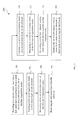
FIGS. 4A and 4B are a top views of images provided in one or more steps of the process of FIG. 3.
FIG. 5 is an exemplary embodiment of an overlay error map used and/or generated by the lithography process of FIG. 3.
DETAILED DESCRIPTION
It is to be understood that the following disclosure provides many different embodiments, or examples, for implementing different features of the invention. Specific examples of components and arrangements are described below to simplify the present disclosure. These are, of course, merely examples and are not intended to be limiting. Moreover, the performance of a first process before a second process in the description that follows may include embodiments in which the second process is performed immediately after the first process, and may also include embodiments in which additional processes may be performed between the first and second processes. Various features may be arbitrarily drawn in different scales for the sake of simplicity and clarity. Furthermore, the formation of a first feature over or on a second feature in the description that follows may include embodiments in which the first and second features are formed in direct contact, and may also include embodiments in which additional features may be formed between the first and second features, such that the first and second features may not be in direct contact.
Referring to FIG. 1, a lithography system 10 includes a radiation source 20, an illuminator 30, a mask 40 (in the present disclosure, the terms of mask, photomask, and reticle are used to refer to the same item), a projection optics box 50 and a target 60 such as a semiconductor wafer on a substrate stage. However, other configurations and inclusion or omission of devices may be possible.
In the present embodiment, the radiation source 20 may be any suitable light source, such as a Krypton Fluoride (KrF) excimer laser with wavelength of 248 nm, an Argon Fluoride (ArF) excimer laser with a wavelength of 193 nm, a fluorine dimer (F2) excimer laser with a wavelength of 157 nm, or other light sources having a longer wavelength. The radiation source 20 may include an optical source selected from the group consisting of ultraviolet (UV) source, deep UV (DUV) source, extreme UV (EUV) source, and X-ray source. The radiation source may alternatively include a particle source selected from the group consisting of electron beam (E-Beam) source, ion beam source, and plasma source.
The illuminator 30 may include refractive optics, such as a single lens or a lens system having multiple lenses (zone plates) and/or reflective optics, such as a single mirror or a mirror system having multiple mirrors in order to direct light from the radiation source 20 onto the mask 40.
The mask 40 can be a transmissive mask or a reflective mask. The mask 40 includes a patterned absorption (opaque) layer. A light beam may be partially or completely blocked when directed on an opaque region. The opaque layer may be patterned to have one or more openings through which a light beam may travel through (for a transmissive mask) or reflect from a reflective region (for a reflective mask). The mask 40 may incorporate other resolution enhancement techniques such as phase shift mask (PSM) and/or optical proximity correction (OPC).
The projection optics box 50 may have refractive optics or reflective optics. The projection optics box 50 directs the patterned radiation towards the target 60 (e.g., a semiconductor wafer).
The target 60 includes a semiconductor wafer with a resist layer, which is sensitive to the radiation. The target 60 may be held by a target substrate stage. The target substrate stage provides control of the target substrate position such that the image of the mask is scanned onto the target substrate in a repetitive fashion (though other lithography methods are possible).
FIG. 2 is a simplified block diagram of an embodiment of a mask manufacturing system 100. The mask manufacturing system 100 includes a plurality of entities, such as a design house 120 and a mask house 130. The plurality of entities are connected by a communications network, which may be a single network or a variety of different networks, such as an intranet and the Internet, and may include wired and/or wireless communication channels. Each entity may interact with other entities and may provide services to and/or receive services from the other entities.
The design house (or design team) 120 generates an IC design layout 122. The IC design layout 122 includes various geometrical patterns designed for an IC product, based on a specification of the IC product to be manufactured. The design house 120 implements a proper design procedure to form the IC design layout 122. The design procedure may include logic design, physical design, and/or place and route. The IC design layout 122 is presented in one or more data files having information of the geometrical patterns. For example, the IC design layout 122 can be expressed in a GDSII file format (or DFII file format).
The mask house 130 (or mask shop) uses the IC design layout 122 to manufacture one or more masks to be used for fabricating the various layers of the IC product according to the IC design layout 122. The mask house 130 performs mask data preparation 132, where the IC design layout 122 is translated into a form that can be physically written by a mask writer, and mask fabrication 144, where the design layout prepared by the mask data preparation 132 is modified to comply with a particular mask writer and/or mask manufacturer and is then fabricated. In the present embodiment, the mask data preparation 132 and mask fabrication 144 are illustrated as separate elements, however, the mask data preparation 132 and mask fabrication 144 can be collectively referred to as mask data preparation.
The mask data preparation 132 includes an optical proximity correction (OPC) 138, and a lithography process check (LPC) 140. The OPC 138 is a lithography enhancement technique used to compensate for image errors, such as those that can arise from diffraction, interference, or other process effects. OPC 138 may add features, such as scattering bars, serif, and/or hammerheads to the IC design layout 122 according to optical models or rules such that, after a lithography process, a final pattern on a wafer is improved with enhanced resolution and precision.
The LPC 140 simulates processing that will be implemented by the IC manufacturer to fabricate ICs. The LPC 140 simulates this processing based on the IC design layout 122 to create a simulated manufactured device. The simulated manufactured device includes simulated contours of all or a portion of the IC design layout. In the present embodiment, the LPC 140 simulates processing of the modified IC design layout, which has been subjected to the OPC 138. The LPC 140 uses one or more LPC models (or rules) 142. The LPC models (or rules) 142 may be based on actual processing parameters of the IC manufacturer. The processing parameters can include parameters associated with various processes of the IC manufacturing cycle, parameters associated with tools used for manufacturing the IC, and/or other aspects of the manufacturing process.
FIG. 3 is a flowchart of a lithography process 200 performed by the lithography system 10 of FIG. 1 and the mask fabricating system 100 of FIG. 2, according to various embodiments. The lithography process 200 in FIG. 3 is an overview and details associated with each step in the process will be described in association with the subsequent figures in the present disclosure.
The method 200 begins at step 202 by providing two lithographic exposure tools (a first exposure tool and a second exposure tool), receiving a first mask fabricated by a mask writer with a first grid table for exposing a first layer on the first exposure tool and a second mask fabricated by a mask writer with a second grid table for exposing a second layer on the second exposure tool from a mask house and providing a substrate 300 with a set of baseline registration marks 310. The substrate 300 includes a semiconductor substrate having an elementary semiconductor such as crystal silicon, polycrystalline silicon, amorphous silicon and germanium, a compound semiconductor such as silicon carbide and gallium arsenic, an alloy semiconductor such as SiGe, GaAsP, AlInAs, AlGaAs, and GaInP, or a combination thereof. The set of baseline registration marks 310 may be formed by deposition, patterning and etching processes known in the art. The set of baseline registration marks 310 includes various configurations, such as box-in-box, frame-in-frame and cross-in-box. >>>>>>The method 200 begins at step 202 by receiving a first mask fabricated by a first mask writer with a first grid table for exposing a first layer on a first exposure tool and a second mask fabricated by a second mask writer with a second grid table for exposing a second layer on a second exposure tool from a mask house and receiving a substrate 300 with a set of baseline registration marks 310. The substrate 300 includes a semiconductor substrate having an elementary semiconductor such as crystal silicon, polycrystalline silicon, amorphous silicon and germanium, a compound semiconductor such as silicon carbide and gallium arsenic, an alloy semiconductor such as SiGe, GaAsP, AlInAs, AlGaAs, and GaInP, or a combination thereof. The set of baseline registration marks 310 may be formed by deposition, patterning, and etching processes known in the art. The set of baseline registration marks 310 includes various configurations, such as box-in-box, frame-in-frame, and cross-in-box.
The first exposure tool and the second exposure tool may be equipped with any suitable optical source, such as ultraviolet (UV) source, deep UV (DUV) source, extreme UV (EUV) source, and X-ray source or other optical sources having longer wavelengths. The first exposure tool may have fairly different process capabilities than those of the second exposure tool, such as having different field distortion signature and resolution. The first exposure tool and the second exposure tool may come from two different exposure tool suppliers. The first exposure tool and the second exposure tool may include a high-end exposure tool and a lower-resolution exposure tool. Because of the high cost of a high-end exposure tool, an IC manufacturing usually uses the high-end exposure tool for critical layers and the lower-resolution exposure tool for less critical layers, which results in different layers being exposed on different exposure tools. In the present embodiment, The first exposure tool and the second exposure tool are assigned to expose two different layers.
The first mask and the second mask are received from a mask house, such as the mask house 130. The first mask and the second mask may be of similar or different types, including transmissive masks and reflective masks. The transmissive mask usually includes a transparent substrate and a patterned absorption layer. The reflective mask usually includes a substrate, a reflective multilayer (ML), and a patterned absorption layer. A light beam from an optical source may be partially or almost completely absorbed when directed onto the absorption layer. The absorption layer may be patterned to have one or more openings through which a light beam may travel through the transparent substrate (for a transmissive mask) or reflect from the reflective ML (for a reflective mask). In the present embodiment, the first mask and the second mask may be of a same type or of different types. The first mask is provided by the mask house 130 with the first grid table configured for the first exposure tool. Similarly, the second mask is provided by the mask house 130 with the second grid table configured for the second exposure tool. The first mask and the second mask may be written by a same mask writer or by two different mask writers.
Referring to FIG. 4A, the method 200 proceeds to step 204 by forming a first set of registration marks 410 on a first photo-sensitive layer (e.g., photoresist, or simply “resist”) on the substrate 300 by using the first mask and the first exposure tool. The first resist layer is deposited on the substrate 300 by any proper techniques, such as a spin-on technique. The first resist layer receives a patterned light exposure from the first mask by using the first exposure tool. The light causes a chemical change in exposed regions of the first resist layer, which may increase or decrease solubility of the exposed regions. If the exposed regions become more soluble, the first resist is referred to as a positive resist. If the exposed regions become less soluble, the first resist is referred to as a negative resist. Baking processes may be performed before or after resist exposure, such as a post-exposure baking process. A developing process selectively removes the exposed or unexposed regions with a developing solution and creating the first set of registration marks 410 on the substrate 300.
The method 200 proceeds to step 206 by measuring a first set of overlay errors of the first set of registration marks 410 with respect to the set of baseline registration marks 310. The first set of overlay errors is measured by an overlay metrology tool. The overlay metrology tool may include an image-based overlay metrology system or a diffraction-based overlay metrology system. For example, the overlay metrology tool is equipped with a camera operable to scan and generate an overlay image. The overlay image is a digitized image of a pair of registration marks, with one registration mark from the first set of registration marks 410 and the other registration mark from the set of baseline registration marks 310. The overlay image is then processed using various image analysis algorithms to determine an overlay error, i.e., the displacement from the center of the outer registration mark to the center of the inner registration mark. By measuring all pairs of registration marks, the first set of overlay errors is obtained, as shown in FIG. 5.
The method 200 proceeds to step 208 by removing the first resist layer from the substrate 300. The first resist layer can be removed by any proper processes, such as plasma dry etch or a wet etch. Since the first set of registration marks 410 is formed on the first resist layer, the first set of registration marks 410 is removed in the removal of the first resist layer.
Referring to FIG. 4B, the method 200 proceeds to step 210 by forming a second set of registration marks 510 on a second resist layer on the substrate 300 by using the second mask and the second exposure tool. The formation of the second set of registration marks 510 on the second resist layer is similar in many respects to those discussed above in step 204.
The method 200 proceeds to step 212 by measuring a second set of overlay errors of the second set of registration marks 510 with respect to the set of baseline registration marks 310. The second set of overlay errors is measured in a similar way in many respects to those discussed above in step 206.
The method 200 proceeds to step 214 by generating a set of tool-induced overlay errors between the first exposure tool and the second exposure tool. The set of tool-induced overlay errors is generated by applying a predetermined algorithm on the first set of overlay errors and the second sets of overlay errors. For example, the set of tool-induced overlay errors is generated by subtracting the second set of overlay errors from the first set of overlay errors (when used for fabricating the first mask). Alternatively, the set of tool-induced overlay errors is generated by subtracting the first set of overlay errors from the second set of overlay errors (when used for fabricating the second mask). The difference between the two sets of overlay errors represents a possible set of tool-induced overlay errors when two exposure tools are assigned to exposure two layers.
The method 200 proceeds to step 216 by sending the set of tool-induced errors to a mask house for fabricating a third mask and then receiving the third mask. The third mask has a grid table adjusted by using the set of tool-induced errors on one of the two grid tables, the first or the second grid table, depending on the first or the second exposure tool to be used. For example, the set of tool-induced overlay errors is used by the mask house 130 to adjust the second grid table to fabricate the third mask. Then the third mask is received and used by the second exposure tool to expose a layer which is needed to align a layer exposed by the first exposure tool. Alternatively, the adjustment is made on the first grid table to fabricate the third mask in the mask house. Then the third mask is received and used by the first exposure tool to expose a layer which is needed to align with a layer exposed by the second exposure tool.
Based on the above, it can be seen that the present disclosure offers a process to reduce tool-induced overlay error between two exposure tools. The process provides a tool overlay matching with flexibility of mask type being used. The process has demonstrated improvements in flexibility in exposure tool's assignment to a specific layer and enhanced manufacture's capability to take advantages of the most advanced exposure tools where they are needed while using lower resolution exposure tool on less critical layers. The process demonstrates overall cost reduction and lifetime extension of lithography tools.
The present disclosure provides many different embodiments. In one embodiment, the present disclosure provides a lithography method. The method comprises receiving a first mask fabricated by a first mask writer with a first grid table, receiving a second mask fabricated by a second mask writer with a second grid table, and receiving a substrate with a set of baseline registration marks. The method also comprises forming a first set of registration marks on the substrate using the first mask and a first exposure tool, measuring a first set of overlay errors of the first set of registration marks with respect to the set of baseline registration marks, removing the first set of registration marks from the substrate, forming a second set of registration marks on the substrate using the second mask and a second exposure tool, measuring a second set of overlay errors of the second set of registration marks with respect to the set of baseline registration marks, generating a set of tool-induced overlay errors from the first set of overlay errors and the second set of overlay errors, sending the set of tool-induced overlay error to a mask maker to fabricate a third mask. In one example, the set of tool-induced overlay errors is generated by subtracting the second set of overlay errors from the first set of overlay errors and the third mask is fabricated by the first mask writer with an adjusted first grid table obtained by subtracting the set of tool-induced overlay errors from the first grid table, wherein the third mask is used on the first exposure tool to expose a layer which is needed to align a layer exposed by the second exposure tool. In another example, the set of tool-induced overlay errors is generated by subtracting the first set of overlay errors from the second set of overlay errors and the third mask is fabricated by the second mask writer with an adjusted second grid table obtained by subtracting the set of tool-induced overlay errors from the second grid table, wherein the third mask is used on the second exposure tool to expose a layer which is needed to align a layer exposed by the first exposure tool.
In another embodiment, the present disclosure provides a method for fabricating a device using a first exposure tool and a second exposure tool. The method comprises receiving a first mask fabricated by a first mask writer with a first grid table for exposing a first layer on the first exposure tool, receiving a second mask fabricated by a second mask writer with a second grid table for exposing a second layer on the second exposure tool, and receiving a substrate with a set of baseline registration marks. The method also includes forming a first resist layer on the substrate, forming a first set of registration marks on the first resist layer using the first mask and the first exposure tool, measuring a first set of overlay errors of the first set of registration marks with respect to the set of baseline registration marks, after measuring the first set of overlay errors, removing the first resist layer and forming a second resist layer on the substrate, forming a second set of registration marks on the second resist layer using the second mask and the second exposure tool, measuring a second set of overlay errors of the second set of registration marks with respect to the set of baseline registration marks, generating a set of tool-induced overlay errors from the first set of overlay errors and the second set of overlay errors, and sending the set of tool-induced overlay error to a mask maker to fabricate a third mask. The method further comprises fabricating the device by one of the following four options, namely using the third mask on the first exposure tool and the second mask on the second exposure tool, or using the third mask on the first exposure tool and a new second mask, which is fabricated by the second mask writer with the second grid table, on the second exposure tool, or using the first mask on the first exposure tool and the third mask on the second exposure tool, or using a new first mask, which is fabricated by the first mask writer with the first grid table, on the first exposure tool and the third mask on the second exposure tool. In one example, the third mask is fabricated by the first mask writer with an adjusted first grid table obtained by subtracting the set of tool-induced overlay errors from the first grid table if the third mask is used on the first exposure tool, wherein the set of tool-induced overlay errors is generated by subtracting the second set of overlay errors from the first set of overlay errors. In another example, the third mask is fabricated by the second mask writer with an adjusted second grid table obtained by subtracting the set of tool-induced overlay errors from the second grid table if the third mask is used on the second exposure tool, wherein the set of tool-induced overlay errors is generated by subtracting the first set of overlay errors from the second set of overlay errors.
In still another embodiment, the present disclosure provides a method that can be used, for example, by a mask house. The method comprises receiving a first set of overlay errors from a first mask used on a first exposure tool, receiving a second set of overlay errors from a second mask used on a second exposure tool, determining a set of tool-induced overlay errors from the first set of overlay errors and the second set of overlay errors, and preparing a third mask based on the set of tool-induced overlay errors. In one example, the first mask is fabricated by using a first grid table and the third mask is fabricated by using an adjusted first grid table obtained by subtracting the set of tool-induced overlay errors from the first grid table, wherein the set of tool-induced overlay errors is obtained by subtracting the second set of overlay errors from the first set of overlay errors, if the third mask is to be used on the first exposure tool for patterning a first layer, which is to be aligned to a second layer exposed on the second exposure tool. In another example, the second mask is fabricated by using a second grid table and the third mask is fabricated by using an adjusted second grid table obtained by subtracting the set of tool-induced overlay errors from the second grid table, wherein the set of tool-induced overlay errors is obtained by subtracting the first set of overlay errors from the second set of overlay errors, if the third mask is to be used for patterning a second layer, which is to be aligned to a first layer exposed on the first exposure tool, on the second exposure tool.
The foregoing outlines features of several embodiments so that those skilled in the art may better understand the aspects of the present disclosure. Those skilled in the art should appreciate that they may readily use the present disclosure as a basis for designing or modifying other processes and structures for carrying out the same purposes and/or achieving the same advantages of the embodiments introduced herein. Those skilled in the art should also realize that such equivalent constructions do not depart from the spirit and scope of the present disclosure, and that they may make various changes, substitutions, and alterations herein without departing from the spirit and scope of the present disclosure.

Claims (16)

What is claimed is:
1. A lithography method comprising:
receiving a first mask fabricated by a first mask writer with a first grid table;
receiving a second mask fabricated by a second mask writer with a second grid table;
receiving a substrate with a set of baseline registration marks;
forming a first set of registration marks on the substrate using the first mask and a first exposure tool;
measuring a first set of overlay errors of the first set of registration marks with respect to the set of baseline registration marks;
removing the first set of registration marks from the substrate;
forming a second set of registration marks on the substrate using the second mask and a second exposure tool;
measuring a second set of overlay errors of the second set of registration marks with respect to the set of baseline registration marks;
generating a set of tool-induced overlay errors from the first set of overlay errors and the second set of overlay errors; and
fabricating a device by using a third mask based on the set of tool-induced overlay errors.
2. The method of claim 1, wherein the first mask writer and the second mask writer are a same mask writer.
3. The method of claim 1, wherein the second mask is a same type of mask as the first mask.
4. The method of claim 1, wherein the second mask is a different type of mask than the first mask.
5. The method of claim 1, wherein the first set of registration marks is formed on a first resist layer on the substrate.
6. The method of claim 5, further comprising:
after measuring the first set of overlay errors, removing the first resist layer; and
forming a second resist layer on the substrate.
7. The method of claim 6, wherein the second set of registration marks is formed on the second resist layer.
8. The method of claim 1, wherein the set of tool-induced overlay errors is generated by subtracting the second set of overlay errors from the first set of overlay errors and the third mask is fabricated by the first mask writer with an adjusted first grid table obtained by subtracting the set of tool-induced overlay errors from the first grid table.
9. The method of claim 8, wherein the third mask is used on the first exposure tool to expose a layer which is needed to align a layer exposed by the second exposure tool.
10. The method of claim 1, wherein the set of tool-induced overlay errors is generated by subtracting the first set of overlay errors from the second set of overlay errors and the third mask is fabricated by the second mask writer with an adjusted second grid table obtained by subtracting the set of tool-induced overlay errors from the second grid table.
11. The method of claim 10, wherein the third mask is used on the second exposure tool to expose a layer which is needed to align a layer exposed by the first exposure tool.
12. A method for fabricating a device using a first exposure tool and a second exposure tool comprising:
receiving a first mask fabricated by a first mask writer with a first grid table for exposing a first layer on the first exposure tool;
receiving a second mask fabricated by a second mask writer with a second grid table for exposing a second layer on the second exposure tool;
receiving a substrate with a set of baseline registration marks;
forming a first resist layer on the substrate;
forming a first set of registration marks on the first resist layer using the first mask and the first exposure tool;
measuring a first set of overlay errors of the first set of registration marks with respect to the set of baseline registration marks;
after measuring the first set of overlay errors, removing the first resist layer and forming a second resist layer on the substrate;
forming a second set of registration marks on the second resist layer using the second mask and the second exposure tool;
measuring a second set of overlay errors of the second set of registration marks with respect to the set of baseline registration marks;
generating a set of tool-induced overlay errors from the first set of overlay errors and the second set of overlay errors; and
fabricating the device by one of the following four options, namely:
using a third mask, based on set of tool-induced overlay errors, on the first exposure tool and the second mask on the second exposure tool; or
using a third mask, based set of tool-induced overlay errors, on the first exposure tool and a new second mask, which is fabricated by the second mask writer with the second grid table, on the second exposure tool; or
using the first mask on the first exposure tool and a third mask, which is based set of tool-induced overlay errors, on the second exposure tool; or
using a new first mask, which is fabricated by the first mask writer with the first grid table, on the first exposure tool and a third mask, which is based set of tool-induced overlay errors, on the second exposure tool.
13. The method of claim 12, wherein the first mask writer and the second mask writer are a same mask writer.
14. The method of claim 12, wherein either the first mask, the second mask, or both the first mask and the second mask is from an outside mask house.
15. The method of claim 12, wherein the third mask is fabricated by the first mask writer with an adjusted first grid table obtained by subtracting the set of tool-induced overlay errors from the first grid table if the third mask is used on the first exposure tool, wherein the set of tool-induced overlay errors is generated by subtracting the second set of overlay errors from the first set of overlay errors.
16. The method of claim 12, wherein the third mask is fabricated by the second mask writer with an adjusted second grid table obtained by subtracting the set of tool-induced overlay errors from the second grid table if the third mask is used on the second exposure tool, wherein the set of tool-induced overlay errors is generated by subtracting the first set of overlay errors from the second set of overlay errors.
US13/832,945 2013-03-15 2013-03-15 Lithography process Expired - Fee Related US9052595B2 (en)

Priority Applications (2)

Application Number Priority Date Filing Date Title
US13/832,945 US9052595B2 (en) 2013-03-15 2013-03-15 Lithography process
US14/733,719 US9869939B2 (en) 2013-03-15 2015-06-08 Lithography process

Applications Claiming Priority (1)

Application Number Priority Date Filing Date Title
US13/832,945 US9052595B2 (en) 2013-03-15 2013-03-15 Lithography process

Related Child Applications (1)

Application Number Title Priority Date Filing Date
US14/733,719 Continuation US9869939B2 (en) 2013-03-15 2015-06-08 Lithography process

Publications (2)

Publication Number Publication Date
US20140272718A1 US20140272718A1 (en) 2014-09-18
US9052595B2 true US9052595B2 (en) 2015-06-09

Family

ID=51528527

Family Applications (2)

Application Number Title Priority Date Filing Date
US13/832,945 Expired - Fee Related US9052595B2 (en) 2013-03-15 2013-03-15 Lithography process
US14/733,719 Active 2033-07-03 US9869939B2 (en) 2013-03-15 2015-06-08 Lithography process

Family Applications After (1)

Application Number Title Priority Date Filing Date
US14/733,719 Active 2033-07-03 US9869939B2 (en) 2013-03-15 2015-06-08 Lithography process

Country Status (1)

Country Link
US (2) US9052595B2 (en)

Families Citing this family (61)

* Cited by examiner, † Cited by third party
Publication number Priority date Publication date Assignee Title
US9733577B2 (en) * 2015-09-03 2017-08-15 Taiwan Semiconductor Manufacturing Co., Ltd. Intra-field process control for lithography
CN110235061B (en) 2017-01-31 2021-06-18 Asml荷兰有限公司 Method and system for increasing accuracy of pattern positioning
US10962873B2 (en) 2017-09-29 2021-03-30 Taiwan Semiconductor Manufacturing Co., Ltd. Extreme ultraviolet mask and method of manufacturing the same
US10451979B2 (en) 2017-09-29 2019-10-22 Taiwan Semiconductor Manufacturing Co., Ltd. Apparatus for EUV lithography and method of measuring focus
US10969690B2 (en) 2017-09-29 2021-04-06 Taiwan Semiconductor Manufacturing Co., Ltd. Extreme ultraviolet control system for adjusting droplet illumination parameters
US10342109B2 (en) 2017-11-14 2019-07-02 Taiwan Semiconductor Manufacturing Co., Ltd. Apparatus and method for generating extreme ultraviolet radiation
US11013097B2 (en) 2017-11-15 2021-05-18 Taiwan Semiconductor Manufacturing Co., Ltd. Apparatus and method for generating extreme ultraviolet radiation
US11617255B2 (en) 2017-11-15 2023-03-28 Taiwan Semiconductor Manufacturing Co., Ltd. Droplet generator and method of servicing extreme ultraviolet imaging tool
US11588293B2 (en) 2017-11-21 2023-02-21 Taiwan Semiconductor Manufacturing Co., Ltd. Methods and systems for aligning master oscillator power amplifier systems
US10642158B2 (en) 2017-11-29 2020-05-05 Taiwan Semiconductor Manufacturing Co., Ltd. Method of controlling reticle masking blade positioning to minimize impact on critical dimension uniformity and device for controlling reticle masking blade positioning
US11143951B2 (en) 2018-04-30 2021-10-12 Taiwan Semiconductor Manufacturing Co., Ltd. Pellicle for an EUV lithography mask and a method of manufacturing thereof
US11143954B2 (en) 2018-06-26 2021-10-12 Taiwan Semiconductor Manufacturing Co., Ltd. Mask patterns and method of manufacture
US10859928B2 (en) 2018-06-28 2020-12-08 Taiwan Semiconductor Manufacturing Co., Ltd. EUV light source and apparatus for lithography
US10955752B2 (en) 2018-06-28 2021-03-23 Taiwan Semiconductor Manufacturing Co., Ltd. EUV radiation source apparatus for lithography
US11249384B2 (en) 2018-06-29 2022-02-15 Taiwan Semiconductor Manufacturing Co., Ltd. Mask for EUV lithography and method of manufacturing the same
US10719020B2 (en) 2018-06-29 2020-07-21 Taiwan Semiconductor Manufacturing Co., Ltd. Droplet generator and method of servicing extreme ultraviolet radiation source apparatus
US10520833B1 (en) 2018-07-13 2019-12-31 Taiwan Semiconductor Manufacturing Co., Ltd. Extreme ultraviolet lithography system
US10871719B2 (en) 2018-08-17 2020-12-22 Taiwan Semiconductor Manufacturing Co., Ltd. EUV metal droplet catchers
US10877190B2 (en) 2018-08-17 2020-12-29 Taiwan Semiconductor Manufacturing Co., Ltd. Extreme ultraviolet radiation source
US10802406B2 (en) 2018-08-17 2020-10-13 Taiwan Semiconductor Manufacturing Co., Ltd. Apparatus and method for generating extreme ultraviolet radiation
US11153959B2 (en) 2018-08-17 2021-10-19 Taiwan Semiconductor Manufacturing Co., Ltd. Apparatus and method for generating extreme ultraviolet radiation
US11016383B2 (en) 2018-08-31 2021-05-25 Taiwan Semiconductor Manufacturing Co., Ltd. Pellicle for an EUV lithography mask and a method of manufacturing thereof
CN109062000A (en) * 2018-08-31 2018-12-21 京东方科技集团股份有限公司 Mask process and mask board group
US11262659B2 (en) 2018-08-31 2022-03-01 Taiwan Semiconductor Manufacturing Co., Ltd. Method of cleaning extreme ultraviolet lithography collector
US10809613B2 (en) 2018-09-25 2020-10-20 Taiwan Semiconductor Manufacturing Co., Ltd. Mask for EUV lithography and method of manufacturing the same
US10747119B2 (en) 2018-09-28 2020-08-18 Taiwan Semiconductor Manufacturing Co., Ltd. Apparatus and method for monitoring reflectivity of the collector for extreme ultraviolet radiation source
US11119398B2 (en) 2018-09-28 2021-09-14 Taiwan Semiconductor Manufacturing Co., Ltd. EUV photo masks
US10871721B2 (en) 2018-09-28 2020-12-22 Taiwan Semiconductor Manufacturing Co., Ltd. Mask blank for lithography and method of manufacturing the same
US10962885B2 (en) 2018-09-28 2021-03-30 Taiwan Semiconductor Manufacturing Co., Ltd. Extreme ultraviolet (EUV) polarization splitter
US11029324B2 (en) 2018-09-28 2021-06-08 Taiwan Semiconductor Manufacturing Co., Ltd. Particle image velocimetry of extreme ultraviolet lithography systems
US11106126B2 (en) 2018-09-28 2021-08-31 Taiwan Semiconductor Manufacturing Co., Ltd. Method of manufacturing EUV photo masks
DE102019110706A1 (en) 2018-09-28 2020-04-02 Taiwan Semiconductor Manufacturing Co., Ltd. METHOD FOR PRODUCING EUV PHOTO MASKS
US10877378B2 (en) 2018-09-28 2020-12-29 Taiwan Semiconductor Manufacturing Co., Ltd. Vessel for extreme ultraviolet radiation source
DE102019124781A1 (en) 2018-09-28 2020-04-02 Taiwan Semiconductor Manufacturing Co., Ltd. METHOD FOR PRODUCING AND TREATING A PHOTOMASK
US11360384B2 (en) 2018-09-28 2022-06-14 Taiwan Semiconductor Manufacturing Co., Ltd. Method of fabricating and servicing a photomask
US10880980B2 (en) 2018-09-28 2020-12-29 Taiwan Semiconductor Manufacturing Co., Ltd. EUV light source and apparatus for EUV lithography
US11452197B2 (en) 2018-10-29 2022-09-20 Taiwan Semiconductor Manufacturing Co., Ltd. Shock wave visualization for extreme ultraviolet plasma optimization
US10527926B1 (en) 2018-10-31 2020-01-07 Taiwan Semiconductor Manufacturing Co., Ltd. Pressurized tin collection bucket with in-line draining mechanism
US11215918B2 (en) * 2019-07-30 2022-01-04 Taiwan Semiconductor Manufacturing Co., Ltd. Method of critical dimension control by oxygen and nitrogen plasma treatment in EUV mask
US11454881B2 (en) 2019-07-31 2022-09-27 Taiwan Semiconductor Manufacturing Co., Ltd. Pellicle design for mask application
US11448956B2 (en) 2019-09-05 2022-09-20 Taiwan Semiconductor Manufacturing Co., Ltd. EUV mask
US11531262B2 (en) 2019-12-30 2022-12-20 Taiwan Semiconductor Manufacturing Co., Ltd. Mask blanks and methods for depositing layers on mask blank
US11294292B2 (en) 2019-12-30 2022-04-05 Taiwan Semiconductor Manufacturing Co., Ltd. Particle removing assembly and method of cleaning mask for lithography
US11150559B2 (en) 2019-12-30 2021-10-19 Taiwan Semiconductor Manufacturing Co., Ltd. Laser interference fringe control for higher EUV light source and EUV throughput
US11768431B2 (en) 2019-12-31 2023-09-26 Taiwan Semiconductor Manufacturing Co., Ltd. Method of fast surface particle and scratch detection for EUV mask backside
US11442356B2 (en) 2020-05-11 2022-09-13 Taiwan Semiconductor Manufacturing Co., Ltd. Lithography mask with an amorphous capping layer
US11829062B2 (en) 2020-05-22 2023-11-28 Taiwan Semiconductor Manufacturing Company, Ltd. EUV photo masks and manufacturing method thereof
CN113253563A (en) * 2020-05-26 2021-08-13 台湾积体电路制造股份有限公司 EUV photomask and method of manufacturing the same
US11506969B2 (en) 2020-05-26 2022-11-22 Taiwan Semiconductor Manufacturing Co., Ltd. EUV photo masks and manufacturing method thereof
US11619875B2 (en) 2020-06-29 2023-04-04 Taiwan Semiconductor Manufacturing Co., Ltd. EUV photo masks and manufacturing method thereof
US11340531B2 (en) 2020-07-10 2022-05-24 Taiwan Semiconductor Manufacturing Company, Ltd. Target control in extreme ultraviolet lithography systems using aberration of reflection image
US11150564B1 (en) 2020-09-29 2021-10-19 Taiwan Semiconductor Manufacturing Co., Ltd. EUV wafer defect improvement and method of collecting nonconductive particles
US11275317B1 (en) 2021-02-26 2022-03-15 Taiwan Semiconductor Manufacturing Co., Ltd. Droplet generator and method of servicing a photolithographic tool
US11415879B1 (en) 2021-03-05 2022-08-16 Taiwan Semiconductor Manufacturing Co., Ltd. Reticle enclosure for lithography systems
US11561482B2 (en) 2021-06-18 2023-01-24 Taiwan Semiconductor Manufacturing Company, Ltd. Methods and apparatus for reducing hydrogen permeation from lithographic tool
US11550229B1 (en) 2021-06-18 2023-01-10 Taiwan Semiconductor Manufacturing Company, Ltd. Enhancing lithography operation for manufacturing semiconductor devices
US11605477B1 (en) 2021-08-27 2023-03-14 Taiwan Semiconductor Manufacturing Company, Ltd. EUV lithography apparatus
US11602037B1 (en) 2021-08-27 2023-03-07 Taiwan Semiconductor Manufacturing Company, Ltd. Apparatus and method for generating extreme ultraviolet radiation
US11520246B1 (en) 2021-08-30 2022-12-06 Taiwan Semiconductor Manufacturing Company, Ltd. Highly efficient automatic particle cleaner method for EUV systems
US11747735B2 (en) 2021-08-31 2023-09-05 Taiwan Semiconductor Manufacturing Company, Ltd. EUV vessel perimeter flow auto adjustment
US11852978B2 (en) 2022-03-07 2023-12-26 Taiwan Semiconductor Manufacturing Company, Ltd. EUV lithography system with 3D sensing and tunning modules

Citations (9)

* Cited by examiner, † Cited by third party
Publication number Priority date Publication date Assignee Title
US20050193362A1 (en) * 2004-03-01 2005-09-01 Phan Khoi A. Multi-layer overlay measurement and correction technique for IC manufacturing
US20070052940A1 (en) * 2005-09-06 2007-03-08 Asml Netherlands B. V. Lithographic method
US20070076205A1 (en) * 2005-09-30 2007-04-05 Bernd Schulz Structure and method for simultaneously determining an overlay accuracy and pattern placement error
US20080030701A1 (en) * 2006-08-03 2008-02-07 Asml Netherlands B.V. Individual wafer history storage for overlay corrections
US20080057418A1 (en) * 2006-08-31 2008-03-06 Rolf Seltmann Method and system for reducing overlay errors within exposure fields by apc control strategies
US20120154773A1 (en) * 2010-12-17 2012-06-21 Carl Zeiss Sms Gmbh Method and apparatus for correcting errors on a wafer processed by a photolithographic mask
US20120244459A1 (en) * 2011-03-24 2012-09-27 Nanya Technology Corp. Method for evaluating overlay error and mask for the same
US20130054186A1 (en) * 2011-08-30 2013-02-28 Asml Netherlands B.V. Method and Apparatus for Determining an Overlay Error
US20130335718A1 (en) * 2011-03-21 2013-12-19 Li Fang Method for measuring distortion of projection objective

Family Cites Families (2)

* Cited by examiner, † Cited by third party
Publication number Priority date Publication date Assignee Title
US7160654B2 (en) * 2003-12-02 2007-01-09 Taiwan Semiconductor Manufacturing Co., Ltd. Method of the adjustable matching map system in lithography
US8804137B2 (en) * 2009-08-31 2014-08-12 Kla-Tencor Corporation Unique mark and method to determine critical dimension uniformity and registration of reticles combined with wafer overlay capability

Patent Citations (10)

* Cited by examiner, † Cited by third party
Publication number Priority date Publication date Assignee Title
US20050193362A1 (en) * 2004-03-01 2005-09-01 Phan Khoi A. Multi-layer overlay measurement and correction technique for IC manufacturing
US20070052940A1 (en) * 2005-09-06 2007-03-08 Asml Netherlands B. V. Lithographic method
US20070076205A1 (en) * 2005-09-30 2007-04-05 Bernd Schulz Structure and method for simultaneously determining an overlay accuracy and pattern placement error
US20080030701A1 (en) * 2006-08-03 2008-02-07 Asml Netherlands B.V. Individual wafer history storage for overlay corrections
US20080057418A1 (en) * 2006-08-31 2008-03-06 Rolf Seltmann Method and system for reducing overlay errors within exposure fields by apc control strategies
US20120154773A1 (en) * 2010-12-17 2012-06-21 Carl Zeiss Sms Gmbh Method and apparatus for correcting errors on a wafer processed by a photolithographic mask
US20140036243A1 (en) * 2010-12-17 2014-02-06 Carl Zeiss Sms Ltd. Method and apparatus for correcting errors on a wafer processed by a photolithographic mask
US20130335718A1 (en) * 2011-03-21 2013-12-19 Li Fang Method for measuring distortion of projection objective
US20120244459A1 (en) * 2011-03-24 2012-09-27 Nanya Technology Corp. Method for evaluating overlay error and mask for the same
US20130054186A1 (en) * 2011-08-30 2013-02-28 Asml Netherlands B.V. Method and Apparatus for Determining an Overlay Error

Also Published As

Publication number Publication date
US20150268565A1 (en) 2015-09-24
US20140272718A1 (en) 2014-09-18
US9869939B2 (en) 2018-01-16

Similar Documents

Publication Publication Date Title
US9869939B2 (en) Lithography process
CN109582995B (en) Integrated circuit manufacturing method and system
JP5198588B2 (en) Method and apparatus for enhancing signal strength for improved generation and placement of model-based sub-resolution assist patterns (MB-SRAF)
JP4464365B2 (en) Apparatus, method, and computer program for performing optical proximity effect correction considering influence of neighborhood
TWI519901B (en) A lithography model for 3d resist profile simulations
US10417376B2 (en) Source beam optimization method for improving lithography printability
KR100927454B1 (en) Feature Optimization with Enhanced Interference Mapping Lithography
TWI448824B (en) A method, program product and apparatus for performing decomposition of a pattern for use in a dpt process
KR20040065185A (en) Method of optical proximity correction design for contact hole mask
TWI742184B (en) Target optimization method
TWI778305B (en) Method for determining patterning device pattern based on manufacturability
KR101437575B1 (en) Substrate-topography-aware lithography modeling
KR102257460B1 (en) Lithography process monitoring method
KR20050043714A (en) A method for performing transmission tuning of a mask pattern to improve process latitude
TWI495961B (en) A lithography model for 3d topographic wafers
TWI759660B (en) Method of determining a mask pattern and related non-transitory computer program product
JP3296296B2 (en) Exposure method and exposure apparatus
KR20210056413A (en) High numerical aperture through-slit source mask optimization method
US9673111B2 (en) Methods for extreme ultraviolet mask defect mitigation by multi-patterning
WO2023016752A1 (en) Match the aberration sensitivity of the metrology mark and the device pattern

Legal Events

Date Code Title Description
AS Assignment

Owner name: TAIWAN SEMICONDUCTOR MANUFACTURING COMPANY, LTD.,

Free format text: ASSIGNMENT OF ASSIGNORS INTEREST;ASSIGNORS:YU, SHINN-SHENG;YEN, ANTHONY;SIGNING DATES FROM 20130721 TO 20130722;REEL/FRAME:031338/0803

STCF Information on status: patent grant

Free format text: PATENTED CASE

MAFP Maintenance fee payment

Free format text: PAYMENT OF MAINTENANCE FEE, 4TH YEAR, LARGE ENTITY (ORIGINAL EVENT CODE: M1551); ENTITY STATUS OF PATENT OWNER: LARGE ENTITY

Year of fee payment: 4

FEPP Fee payment procedure

Free format text: MAINTENANCE FEE REMINDER MAILED (ORIGINAL EVENT CODE: REM.); ENTITY STATUS OF PATENT OWNER: LARGE ENTITY

LAPS Lapse for failure to pay maintenance fees

Free format text: PATENT EXPIRED FOR FAILURE TO PAY MAINTENANCE FEES (ORIGINAL EVENT CODE: EXP.); ENTITY STATUS OF PATENT OWNER: LARGE ENTITY

STCH Information on status: patent discontinuation

Free format text: PATENT EXPIRED DUE TO NONPAYMENT OF MAINTENANCE FEES UNDER 37 CFR 1.362

FP Lapsed due to failure to pay maintenance fee

Effective date: 20230609