US9240470B2 - High-performance reverse-conduction field-stop (RCFS) insulated gate bipolar transistor and method for manufacturing the same - Google Patents

High-performance reverse-conduction field-stop (RCFS) insulated gate bipolar transistor and method for manufacturing the same Download PDF

Info

Publication number
US9240470B2
US9240470B2 US14/526,090 US201414526090A US9240470B2 US 9240470 B2 US9240470 B2 US 9240470B2 US 201414526090 A US201414526090 A US 201414526090A US 9240470 B2 US9240470 B2 US 9240470B2
Authority
US
United States
Prior art keywords
conductive type
substrate
type substrate
ion implantation
igbt
Prior art date
Legal status (The legal status is an assumption and is not a legal conclusion. Google has not performed a legal analysis and makes no representation as to the accuracy of the status listed.)
Active
Application number
US14/526,090
Other versions
US20150279980A1 (en
Inventor
Mei-Ling Chen
Hung-Hsin Kuo
Yi-Lun HSIA
Chung-Chen Chang
Current Assignee (The listed assignees may be inaccurate. Google has not performed a legal analysis and makes no representation or warranty as to the accuracy of the list.)
PFC DEVICE HOLDINGS Ltd
Original Assignee
PFC DEVICE HOLDINGS Ltd
Priority date (The priority date is an assumption and is not a legal conclusion. Google has not performed a legal analysis and makes no representation as to the accuracy of the date listed.)
Filing date
Publication date
Application filed by PFC DEVICE HOLDINGS Ltd filed Critical PFC DEVICE HOLDINGS Ltd
Assigned to PFC DEVICE HOLDINGS LIMITED reassignment PFC DEVICE HOLDINGS LIMITED ASSIGNMENT OF ASSIGNORS INTEREST (SEE DOCUMENT FOR DETAILS). Assignors: CHANG, CHUNG-CHEN, CHEN, MEI-LING, HSIA, YI-LUN, KUO, HUNG-HSIN
Publication of US20150279980A1 publication Critical patent/US20150279980A1/en
Application granted granted Critical
Publication of US9240470B2 publication Critical patent/US9240470B2/en
Active legal-status Critical Current
Anticipated expiration legal-status Critical

Links

Images

Classifications

    • HELECTRICITY
    • H01ELECTRIC ELEMENTS
    • H01LSEMICONDUCTOR DEVICES NOT COVERED BY CLASS H10
    • H01L29/00Semiconductor devices adapted for rectifying, amplifying, oscillating or switching, or capacitors or resistors with at least one potential-jump barrier or surface barrier, e.g. PN junction depletion layer or carrier concentration layer; Details of semiconductor bodies or of electrodes thereof  ; Multistep manufacturing processes therefor
    • H01L29/66Types of semiconductor device ; Multistep manufacturing processes therefor
    • H01L29/68Types of semiconductor device ; Multistep manufacturing processes therefor controllable by only the electric current supplied, or only the electric potential applied, to an electrode which does not carry the current to be rectified, amplified or switched
    • H01L29/70Bipolar devices
    • H01L29/72Transistor-type devices, i.e. able to continuously respond to applied control signals
    • H01L29/739Transistor-type devices, i.e. able to continuously respond to applied control signals controlled by field-effect, e.g. bipolar static induction transistors [BSIT]
    • H01L29/7393Insulated gate bipolar mode transistors, i.e. IGBT; IGT; COMFET
    • H01L29/7395Vertical transistors, e.g. vertical IGBT
    • H01L29/7396Vertical transistors, e.g. vertical IGBT with a non planar surface, e.g. with a non planar gate or with a trench or recess or pillar in the surface of the emitter, base or collector region for improving current density or short circuiting the emitter and base regions
    • HELECTRICITY
    • H01ELECTRIC ELEMENTS
    • H01LSEMICONDUCTOR DEVICES NOT COVERED BY CLASS H10
    • H01L21/00Processes or apparatus adapted for the manufacture or treatment of semiconductor or solid state devices or of parts thereof
    • H01L21/02Manufacture or treatment of semiconductor devices or of parts thereof
    • H01L21/04Manufacture or treatment of semiconductor devices or of parts thereof the devices having at least one potential-jump barrier or surface barrier, e.g. PN junction, depletion layer or carrier concentration layer
    • H01L21/18Manufacture or treatment of semiconductor devices or of parts thereof the devices having at least one potential-jump barrier or surface barrier, e.g. PN junction, depletion layer or carrier concentration layer the devices having semiconductor bodies comprising elements of Group IV of the Periodic System or AIIIBV compounds with or without impurities, e.g. doping materials
    • H01L21/26Bombardment with radiation
    • H01L21/263Bombardment with radiation with high-energy radiation
    • H01L21/265Bombardment with radiation with high-energy radiation producing ion implantation
    • H01L21/26506Bombardment with radiation with high-energy radiation producing ion implantation in group IV semiconductors
    • HELECTRICITY
    • H01ELECTRIC ELEMENTS
    • H01LSEMICONDUCTOR DEVICES NOT COVERED BY CLASS H10
    • H01L21/00Processes or apparatus adapted for the manufacture or treatment of semiconductor or solid state devices or of parts thereof
    • H01L21/02Manufacture or treatment of semiconductor devices or of parts thereof
    • H01L21/04Manufacture or treatment of semiconductor devices or of parts thereof the devices having at least one potential-jump barrier or surface barrier, e.g. PN junction, depletion layer or carrier concentration layer
    • H01L21/18Manufacture or treatment of semiconductor devices or of parts thereof the devices having at least one potential-jump barrier or surface barrier, e.g. PN junction, depletion layer or carrier concentration layer the devices having semiconductor bodies comprising elements of Group IV of the Periodic System or AIIIBV compounds with or without impurities, e.g. doping materials
    • H01L21/30Treatment of semiconductor bodies using processes or apparatus not provided for in groups H01L21/20 - H01L21/26
    • H01L21/324Thermal treatment for modifying the properties of semiconductor bodies, e.g. annealing, sintering
    • HELECTRICITY
    • H01ELECTRIC ELEMENTS
    • H01LSEMICONDUCTOR DEVICES NOT COVERED BY CLASS H10
    • H01L21/00Processes or apparatus adapted for the manufacture or treatment of semiconductor or solid state devices or of parts thereof
    • H01L21/70Manufacture or treatment of devices consisting of a plurality of solid state components formed in or on a common substrate or of parts thereof; Manufacture of integrated circuit devices or of parts thereof
    • H01L21/71Manufacture of specific parts of devices defined in group H01L21/70
    • H01L21/76Making of isolation regions between components
    • H01L21/762Dielectric regions, e.g. EPIC dielectric isolation, LOCOS; Trench refilling techniques, SOI technology, use of channel stoppers
    • H01L21/76224Dielectric regions, e.g. EPIC dielectric isolation, LOCOS; Trench refilling techniques, SOI technology, use of channel stoppers using trench refilling with dielectric materials
    • HELECTRICITY
    • H01ELECTRIC ELEMENTS
    • H01LSEMICONDUCTOR DEVICES NOT COVERED BY CLASS H10
    • H01L29/00Semiconductor devices adapted for rectifying, amplifying, oscillating or switching, or capacitors or resistors with at least one potential-jump barrier or surface barrier, e.g. PN junction depletion layer or carrier concentration layer; Details of semiconductor bodies or of electrodes thereof  ; Multistep manufacturing processes therefor
    • H01L29/02Semiconductor bodies ; Multistep manufacturing processes therefor
    • H01L29/06Semiconductor bodies ; Multistep manufacturing processes therefor characterised by their shape; characterised by the shapes, relative sizes, or dispositions of the semiconductor regions ; characterised by the concentration or distribution of impurities within semiconductor regions
    • H01L29/08Semiconductor bodies ; Multistep manufacturing processes therefor characterised by their shape; characterised by the shapes, relative sizes, or dispositions of the semiconductor regions ; characterised by the concentration or distribution of impurities within semiconductor regions with semiconductor regions connected to an electrode carrying current to be rectified, amplified or switched and such electrode being part of a semiconductor device which comprises three or more electrodes
    • H01L29/083Anode or cathode regions of thyristors or gated bipolar-mode devices
    • H01L29/0834Anode regions of thyristors or gated bipolar-mode devices, e.g. supplementary regions surrounding anode regions
    • HELECTRICITY
    • H01ELECTRIC ELEMENTS
    • H01LSEMICONDUCTOR DEVICES NOT COVERED BY CLASS H10
    • H01L29/00Semiconductor devices adapted for rectifying, amplifying, oscillating or switching, or capacitors or resistors with at least one potential-jump barrier or surface barrier, e.g. PN junction depletion layer or carrier concentration layer; Details of semiconductor bodies or of electrodes thereof  ; Multistep manufacturing processes therefor
    • H01L29/66Types of semiconductor device ; Multistep manufacturing processes therefor
    • H01L29/66007Multistep manufacturing processes
    • H01L29/66075Multistep manufacturing processes of devices having semiconductor bodies comprising group 14 or group 13/15 materials
    • H01L29/66227Multistep manufacturing processes of devices having semiconductor bodies comprising group 14 or group 13/15 materials the devices being controllable only by the electric current supplied or the electric potential applied, to an electrode which does not carry the current to be rectified, amplified or switched, e.g. three-terminal devices
    • H01L29/66234Bipolar junction transistors [BJT]
    • H01L29/66325Bipolar junction transistors [BJT] controlled by field-effect, e.g. insulated gate bipolar transistors [IGBT]
    • H01L29/66333Vertical insulated gate bipolar transistors
    • HELECTRICITY
    • H01ELECTRIC ELEMENTS
    • H01LSEMICONDUCTOR DEVICES NOT COVERED BY CLASS H10
    • H01L21/00Processes or apparatus adapted for the manufacture or treatment of semiconductor or solid state devices or of parts thereof
    • H01L21/02Manufacture or treatment of semiconductor devices or of parts thereof
    • H01L21/04Manufacture or treatment of semiconductor devices or of parts thereof the devices having at least one potential-jump barrier or surface barrier, e.g. PN junction, depletion layer or carrier concentration layer
    • H01L21/18Manufacture or treatment of semiconductor devices or of parts thereof the devices having at least one potential-jump barrier or surface barrier, e.g. PN junction, depletion layer or carrier concentration layer the devices having semiconductor bodies comprising elements of Group IV of the Periodic System or AIIIBV compounds with or without impurities, e.g. doping materials
    • H01L21/26Bombardment with radiation
    • H01L21/263Bombardment with radiation with high-energy radiation
    • H01L21/265Bombardment with radiation with high-energy radiation producing ion implantation
    • H01L21/26506Bombardment with radiation with high-energy radiation producing ion implantation in group IV semiconductors
    • H01L21/26513Bombardment with radiation with high-energy radiation producing ion implantation in group IV semiconductors of electrically active species

Definitions

  • the present invention relates to an insulated gate bipolar transistor and method for manufacturing the same, especially to a high-performance insulated gate bipolar transistor and method for manufacturing the same.
  • Insulated gate bipolar transistor is a semiconductor device combining the features of metal-oxide-semiconductor field effect transistor (MOSFET) and bipolar junction transistor (BJT). IGBT has the advantages of gate-controlling ability of MOSFET and low turn-on voltage of BJT and is thus extensively used in high voltage and high power applications.
  • MOSFET metal-oxide-semiconductor field effect transistor
  • BJT bipolar junction transistor
  • a conventional IGBT such as a punch through (PT) IGBT, mainly comprises a P+ type semiconductor substrate and N-type buffer layer arranged thereon.
  • An N type epitaxial layer is formed on the N-type buffer layer and functions as drain of parasitic MOSFET in the IGBT.
  • a gate and an emitter are formed in the N type epitaxial layer, and a collector is formed on bottom face of the P+ type substrate.
  • the breakdown voltage of the PT IGBT is determined by the P+ type substrate and N-type buffer layer because a maximum electric field is generated therebetween.
  • NPT non-punch through
  • FS field stop
  • a fast return epitaxial diode FLP
  • FRED fast return epitaxial diode
  • a reverse-conducted diode is built-in above mentioned IGBTs for soft switching.
  • This kind of IGBT is referred to as reverse conduction field stop (RCFS) IGBT.
  • the conventional RCFS IGBT is first formed with N+ type doped layer on backside of substrate by using metal mask, then formed with P+ type doped layer functioning as collector, and finally formed with N+ type doped layer and P type doped layer by rapid thermal annealing. Nevertheless, lateral Zener diode tends to form in the RCFS because the N+ doped layer and the P type doped layer are on the same horizontal plane of the backside of the substrate.
  • one object of the present invention is to provide a high-performance insulated gate bipolar transistor (IGBT) with suppression of parasitic Zener diode, and method for manufacturing the IGBT.
  • IGBT insulated gate bipolar transistor
  • a method for manufacturing a high-performance insulated gate bipolar transistor comprising the following steps: (a) providing a first conductive type substrate and manufacturing a semi-finished semiconductor device on a front side of the substrate; (b) covering a front side of the semiconductor device with a protection layer; (c) performing an ion implantation process on back side of the first conductive type substrate to form a first conductive type field stop ion implantation with a field stop depth from a back face of the first conductive type substrate; (d) forming a plurality of trenches on the back side of the first conductive type substrate, each of the trenches having a trench depth smaller than the field stop depth; (e) performing an ion implantation process on back side of the first conductive type substrate to form a first conductive type ion implantation pattern on bottom faces of the trenches; and (f) performing an ion implantation process on back side of the first conductive type substrate to form a second conductive type
  • a method for manufacturing a high-performance insulated gate bipolar transistor comprising the following steps: (a) providing a first conductive type substrate and manufacturing a semi-finished semiconductor device on a front side of the substrate; (b) covering a front side of the semiconductor device with a protection layer; (c) forming a plurality of trenches on the back side of the first conductive type substrate, each of the trenches having a trench depth; (d) performing an ion implantation process on back side of the first conductive type substrate to form a first conductive type ion implantation pattern on bottom faces of the trenches; (e) performing an ion implantation process on back side of the first conductive type substrate to form a second conductive type ion implantation layer on back face of the first conductive type substrate; and (f) performing an ion implantation process on back side of the first conductive type substrate to form a first conductive type field stop ion implantation with a field stop depth from back face
  • a high-performance insulated gate bipolar transistor comprising: a first conductive type substrate; a plurality of trenches defined on a bottom face of the first conductive type substrate; a plurality of first conductive type doping regions formed on bottom faces of the trenches; a second conductive type doping region formed on the bottom face of the first conductive type substrate; and a first conductive type field stop doping region formed in the first conductive type substrate and separated with the bottom face of the first conductive type substrate with a field stop depth, where the field stop depth is larger than a depth of the trench.
  • IGBT insulated gate bipolar transistor
  • the high-performance insulated gate bipolar transistor (IGBT) thus manufactured has a plurality trenches and a first conductive type (either N type or P type) doping regions on bottom faces of the trenches.
  • the subsequent conductive type doping will be either P type or N type respectively. Therefore, the PN junction on backside of the substrate is irregular and Zener diode can be prevented from forming to enhance the performance of the IGBT.
  • FIGS. 1A to 1L show the manufacturing process for the high-performance insulated gate bipolar transistor (IGBT) according to a first embodiment of the present invention.
  • IGBT insulated gate bipolar transistor
  • FIGS. 2A to 2L show the manufacturing process for the high-performance insulated gate bipolar transistor (IGBT) according to a second embodiment of the present invention.
  • IGBT insulated gate bipolar transistor
  • FIGS. 1A to 1L show the manufacturing process for the high-performance insulated gate bipolar transistor (IGBT) according to a first embodiment of the present invention.
  • IGBT insulated gate bipolar transistor
  • FIG. 1A part of standard processes for manufacturing a MOSFET device are first performed on an N type substrate 10 (namely, the front end devices 60 and contact holes 62 shown in this figure are finished, and therefore the MOSFET device is semi-finished), and then, as shown in FIG. 1B , a protection layer 20 (such as binding tape, protection carrier or protection film) is used to cover the front portion of the MOSFET device. More particularly, the MOSFET device shown in FIG. 1A has been finished with the contact hole thereof being etched to 90% and interlayer dielectric being increased with 10% thickness such that the interlayer dielectric can protect the front portion of the IGBT device in later processes.
  • a protection layer 20 such as binding tape, protection carrier or protection film
  • the N type substrate 10 is polished at back side thereof, then stress release wet etching and cleaning are performed for the N type substrate 10 to thin the N type substrate 10 (namely, decrease the thickness of the N type substrate 10 ).
  • the remaining thickness of the N type substrate 10 is relevant to the demanded voltage tolerance for the high-performance IGBT to be manufactured.
  • an ion implantation process is performed to form an N type field stop ion implantation layer 30 on the back side of the N type substrate 10 , where the N type field stop ion implantation layer 30 is separated with the bottom face of the N type substrate 10 by a field stop depth.
  • a photoresist pattern 42 is formed on the bottom face of the N type substrate 10 and the photoresist pattern 42 is used as mask to etch a plurality of trenches 40 on the back side of the N type substrate 10 .
  • the backside portion of the N type substrate 10 which is not covered by the photoresist pattern 42 , is etched to form the plurality of trenches 40 .
  • each of the trenches 40 has a trench depth and the trench depth is larger than 1 micrometer.
  • the photoresist pattern 42 is used as mask for ion implantation and another ion implantation process is performed on the back side of the N type substrate 10 to form an N type ion implantation pattern 32 .
  • the N type ion implantation pattern 32 is formed on the bottom faces of the trenches, which are not covered by the photoresist pattern 42 . Therefore, the N type ion implantation pattern 32 is separated with the bottom face of the N type substrate 10 by the trench depth, where the field stop depth is larger than the trench depth.
  • the N type field stop ion implantation layer 30 is deeper than the N type ion implantation pattern 32 to provide field stop function.
  • N type field stop doping region 30 ′ As shown in FIGS. 1I and 1J , after removing the protection layer 20 , cleaning process with DHF and thermal annealing process are performed to form N type field stop doping region 30 ′, N type doping region 32 ′ and P type doping region 34 ′, respectively.
  • emitter metal layer 50 and gate metal layer 51 are formed on top side of the N type substrate 10 .
  • collector metal layer 52 is formed on bottom side of the N type substrate 10 .
  • the emitter metal layer 50 , the gate metal layer 51 and the collector metal layer 52 can be formed by sputtering process, and the material of the emitter metal layer 50 , the gate metal layer 51 and the collector metal layer 52 can be, but not limited to, aluminum (Al), TiN or tungsten (W).
  • the bottom side of the N type substrate 10 is formed with the plurality of the trenches 40 with trench depth larger than 1 micrometer.
  • the N type doping region 32 ′ is formed on the bottom faces of the trenches 40 such that the N type doping region 32 ′ has sufficient separation with the P type doping region 34 ′ along depth direction. Therefore, the PN junction at the back side of the N type substrate 10 is irregular to prevent the Zener diode from forming and to enhance the performance of the IGBT device.
  • FIGS. 2A to 2L show the manufacturing process for the high-performance insulated gate bipolar transistor (IGBT) according to a second embodiment of the present invention.
  • IGBT insulated gate bipolar transistor
  • FIG. 2A part of standard processes for manufacturing a MOSFET are first performed on an N type substrate 10 (namely, the front end devices 60 and contact holes 62 shown in this figure are finished), and then, as shown in FIG. 2B , a protection layer 20 (such as binding tape, protection carrier or protection film) is used to cover the front portion of the MOSFET device. More particularly, the MOSFET device shown in FIG. 2A has been finished with contact hole being etched to 90% and interlayer dielectric being increased with 10% thickness such that the interlayer dielectric can protect the front portion of the IGBT device in later processes.
  • a protection layer 20 such as binding tape, protection carrier or protection film
  • the N type substrate 10 is polished at back side thereof, then stress release wet etching and cleaning are performed for the N type substrate 10 to thin the N type substrate 10 .
  • the remaining thickness of the N type substrate 10 is relevant to the demanded voltage tolerance for the high-performance IGBT to be manufactured.
  • a photoresist pattern 42 is formed on the bottom face of the N type substrate 10 and the photoresist pattern 42 is used as mask to etch a plurality of trenches 40 on the back side of the N type substrate 10 .
  • the backside portion of the N type substrate 10 which is not covered by the photoresist pattern 42 , is etched to form the plurality of trenches 40 .
  • each of the trenches 40 has a trench depth and the trench depth is larger than 1 micrometer. As shown in FIG.
  • the photoresist pattern 42 is used as mask for ion implantation and an ion implantation process is performed on the back side of the N type substrate 10 to form an N type ion implantation pattern 32 .
  • the N type ion implantation pattern 32 is formed on the bottom faces of the trenches, which are not covered by the photoresist pattern 42 . Therefore, the N type ion implantation pattern 32 is separated with the bottom face of the N type substrate 10 by the trench depth larger than 1 micrometer.
  • FIGS. 2F and 2G after removing the photoresist pattern 42 , another ion implantation process is performed on the back side of the N type substrate 10 to form a P type ion implantation layer 34 on the remaining bottom face of the N type substrate 10 .
  • FIG. 2H still another ion implantation process is performed on the back side of the N type substrate 10 to form an N type field stop ion implantation layer 36 on the back side of the N type substrate 10 .
  • the N type field stop ion implantation layer 36 is separated with the bottom face of the N type substrate 10 by a field stop depth, where the field stop depth is larger than the trench depth.
  • the N type field stop ion implantation layer 36 is deeper than the N type ion implantation pattern 32 to provide field stop function.
  • the N type field stop ion implantation layer 36 is formed after the trenches 40 are defined. Therefore, the N type field stop ion implantation layer 36 in the second embodiment has more fluctuated profile in comparison with the N type field stop ion implantation layer 30 in the first embodiment.
  • N type field stop doping region 36 ′ As shown in FIGS. 21 and 2J , after removing the protection layer 20 , cleaning process with DHF and thermal annealing process are performed to form N type field stop doping region 36 ′, N type doping region 32 ′ and P type doping region 34 ′, respectively.
  • emitter metal layer 50 and gate metal layer 51 are formed on top side of the N type substrate 10 .
  • collector metal layer 52 is formed on bottom side of the N type substrate 10 .
  • the emitter metal layer 50 , the gate metal layer 51 and the collector metal layer 52 can be formed by sputtering process, and the material of the emitter metal layer 50 , the gate metal layer 51 and the collector metal layer 52 can be, but not limited to, aluminum (Al), TiN or tungsten (W).
  • the bottom side of the N type substrate 10 is formed with the plurality of the trenches 40 with trench depth larger than 1 micrometer.
  • the N type doping region 32 ′ is formed on the bottom of the trenches 40 such that the N type doping region 32 ′ has sufficient separation with the P type doping region 34 ′ along the depth direction. Therefore, the PN junction at the back side of the N type substrate 10 is irregular to prevent the Zener diode from forming and to enhance the performance of the IGBT device.
  • the N type field stop doping region 36 ′ also has fluctuated profile to further prevent the forming of the Zener diode.
  • the present invention is descried with above mentioned embodiment.
  • the skilled in the related art can easily know the present invention has additional variations and embodiments.
  • the N type substrate 10 can be replaced with P type substrate, and the original N type doping is replaced by P type doping.
  • the original P type doping is replaced by N type doping.
  • This kind of variation can still have the effect to prevent the forming of the Zener diode.

Abstract

A high-performance reverse-conduction field-stop (RCFS) insulated gate bipolar transistor (IGBT) includes a first conductive type substrate, a plurality of trenches defined on a bottom face of the substrate, a plurality of first conductive type doping regions formed on bottom face of the trenches, a second conductive type doping region formed on bottom face of the substrate, and a first conductive type field stop doping region formed in the substrate and separated from the bottom face of the substrate by a field stop depth, where the field stop depth is larger than a depth of the trench. Due to a separation between the first conductive type doping regions and the second conductive type doping region, Zener diode can be prevented from forming on bottom side of the substrate and the performance of IGBT can be accordingly enhanced.

Description

BACKGROUND OF THE INVENTION
1. Field of the Invention
The present invention relates to an insulated gate bipolar transistor and method for manufacturing the same, especially to a high-performance insulated gate bipolar transistor and method for manufacturing the same.
2. Description of Prior Art
Insulated gate bipolar transistor (IGBT) is a semiconductor device combining the features of metal-oxide-semiconductor field effect transistor (MOSFET) and bipolar junction transistor (BJT). IGBT has the advantages of gate-controlling ability of MOSFET and low turn-on voltage of BJT and is thus extensively used in high voltage and high power applications.
A conventional IGBT, such as a punch through (PT) IGBT, mainly comprises a P+ type semiconductor substrate and N-type buffer layer arranged thereon. An N type epitaxial layer is formed on the N-type buffer layer and functions as drain of parasitic MOSFET in the IGBT. Moreover, a gate and an emitter are formed in the N type epitaxial layer, and a collector is formed on bottom face of the P+ type substrate. The breakdown voltage of the PT IGBT is determined by the P+ type substrate and N-type buffer layer because a maximum electric field is generated therebetween.
Another conventional IGBT, such as a non-punch through (NPT) IGBT, does not use N-type buffer layer. The breakdown voltage of the NPT IGBT is determined by the avalanche mechanism of the N type epitaxial (N drift) layer. To increase the breakdown voltage, field stop (FS) IGBT was developed, where the N-type buffer layer in PT IGBT is replaced by a field stop ion implantation layer. Therefore, the abrupt junction in the PT IGBT is also replaced by a graded (such as a linearly graded) N type profile. The value of the maximum electric field can be advantageously reduced to enhance breakdown voltage.
However, in above-mentioned three types of IGBTs, a fast return epitaxial diode (FRED) is needed to parallel connect with the IGBT to release turn-off current. Therefore, a reverse-conducted diode is built-in above mentioned IGBTs for soft switching. This kind of IGBT is referred to as reverse conduction field stop (RCFS) IGBT. The conventional RCFS IGBT is first formed with N+ type doped layer on backside of substrate by using metal mask, then formed with P+ type doped layer functioning as collector, and finally formed with N+ type doped layer and P type doped layer by rapid thermal annealing. Nevertheless, lateral Zener diode tends to form in the RCFS because the N+ doped layer and the P type doped layer are on the same horizontal plane of the backside of the substrate.
SUMMARY OF THE INVENTION
Accordingly, one object of the present invention is to provide a high-performance insulated gate bipolar transistor (IGBT) with suppression of parasitic Zener diode, and method for manufacturing the IGBT.
According to one aspect of the present invention provides a method for manufacturing a high-performance insulated gate bipolar transistor (IGBT), comprising the following steps: (a) providing a first conductive type substrate and manufacturing a semi-finished semiconductor device on a front side of the substrate; (b) covering a front side of the semiconductor device with a protection layer; (c) performing an ion implantation process on back side of the first conductive type substrate to form a first conductive type field stop ion implantation with a field stop depth from a back face of the first conductive type substrate; (d) forming a plurality of trenches on the back side of the first conductive type substrate, each of the trenches having a trench depth smaller than the field stop depth; (e) performing an ion implantation process on back side of the first conductive type substrate to form a first conductive type ion implantation pattern on bottom faces of the trenches; and (f) performing an ion implantation process on back side of the first conductive type substrate to form a second conductive type ion implantation layer on back face of the first conductive type substrate.
According to another aspect of the present invention provides a method for manufacturing a high-performance insulated gate bipolar transistor (IGBT), comprising the following steps: (a) providing a first conductive type substrate and manufacturing a semi-finished semiconductor device on a front side of the substrate; (b) covering a front side of the semiconductor device with a protection layer; (c) forming a plurality of trenches on the back side of the first conductive type substrate, each of the trenches having a trench depth; (d) performing an ion implantation process on back side of the first conductive type substrate to form a first conductive type ion implantation pattern on bottom faces of the trenches; (e) performing an ion implantation process on back side of the first conductive type substrate to form a second conductive type ion implantation layer on back face of the first conductive type substrate; and (f) performing an ion implantation process on back side of the first conductive type substrate to form a first conductive type field stop ion implantation with a field stop depth from back face of the first conductive type substrate, where the trench depth is smaller than the field stop depth.
According to still another aspect of the present invention provides a high-performance insulated gate bipolar transistor (IGBT), comprising: a first conductive type substrate; a plurality of trenches defined on a bottom face of the first conductive type substrate; a plurality of first conductive type doping regions formed on bottom faces of the trenches; a second conductive type doping region formed on the bottom face of the first conductive type substrate; and a first conductive type field stop doping region formed in the first conductive type substrate and separated with the bottom face of the first conductive type substrate with a field stop depth, where the field stop depth is larger than a depth of the trench.
According the present invention, the high-performance insulated gate bipolar transistor (IGBT) thus manufactured has a plurality trenches and a first conductive type (either N type or P type) doping regions on bottom faces of the trenches. The subsequent conductive type doping will be either P type or N type respectively. Therefore, the PN junction on backside of the substrate is irregular and Zener diode can be prevented from forming to enhance the performance of the IGBT.
BRIEF DESCRIPTION OF DRAWING
The features of the invention believed to be novel are set forth with particularity in the appended claims. The invention itself however may be best understood by referring to the following detailed description of the invention, which describes certain exemplary embodiments of the invention, taken in conjunction with the accompanying drawings in which:
FIGS. 1A to 1L show the manufacturing process for the high-performance insulated gate bipolar transistor (IGBT) according to a first embodiment of the present invention.
FIGS. 2A to 2L show the manufacturing process for the high-performance insulated gate bipolar transistor (IGBT) according to a second embodiment of the present invention.
DETAILED DESCRIPTION OF THE INVENTION
FIGS. 1A to 1L show the manufacturing process for the high-performance insulated gate bipolar transistor (IGBT) according to a first embodiment of the present invention.
As shown in FIG. 1A, part of standard processes for manufacturing a MOSFET device are first performed on an N type substrate 10 (namely, the front end devices 60 and contact holes 62 shown in this figure are finished, and therefore the MOSFET device is semi-finished), and then, as shown in FIG. 1B, a protection layer 20 (such as binding tape, protection carrier or protection film) is used to cover the front portion of the MOSFET device. More particularly, the MOSFET device shown in FIG. 1A has been finished with the contact hole thereof being etched to 90% and interlayer dielectric being increased with 10% thickness such that the interlayer dielectric can protect the front portion of the IGBT device in later processes.
As shown in FIG. 1C, the N type substrate 10 is polished at back side thereof, then stress release wet etching and cleaning are performed for the N type substrate 10 to thin the N type substrate 10 (namely, decrease the thickness of the N type substrate 10). The remaining thickness of the N type substrate 10 is relevant to the demanded voltage tolerance for the high-performance IGBT to be manufactured.
As shown in FIG. 1D, after the backside polishing, an ion implantation process is performed to form an N type field stop ion implantation layer 30 on the back side of the N type substrate 10, where the N type field stop ion implantation layer 30 is separated with the bottom face of the N type substrate 10 by a field stop depth. As shown in FIG. 1E, a photoresist pattern 42 is formed on the bottom face of the N type substrate 10 and the photoresist pattern 42 is used as mask to etch a plurality of trenches 40 on the back side of the N type substrate 10. Namely, the backside portion of the N type substrate 10, which is not covered by the photoresist pattern 42, is etched to form the plurality of trenches 40. Moreover, each of the trenches 40 has a trench depth and the trench depth is larger than 1 micrometer.
As shown in FIG. 1F, the photoresist pattern 42 is used as mask for ion implantation and another ion implantation process is performed on the back side of the N type substrate 10 to form an N type ion implantation pattern 32. Because the trenches 40 are present at this ion implantation process, the N type ion implantation pattern 32 is formed on the bottom faces of the trenches, which are not covered by the photoresist pattern 42. Therefore, the N type ion implantation pattern 32 is separated with the bottom face of the N type substrate 10 by the trench depth, where the field stop depth is larger than the trench depth. In other word, the N type field stop ion implantation layer 30 is deeper than the N type ion implantation pattern 32 to provide field stop function.
As shown in FIGS. 1G and 1H, after removing the photoresist pattern 42, another ion implantation process is performed on the back side of the N type substrate 10 to form an P type ion implantation layer 34 on the remaining bottom face of the N type substrate 10.
As shown in FIGS. 1I and 1J, after removing the protection layer 20, cleaning process with DHF and thermal annealing process are performed to form N type field stop doping region 30′, N type doping region 32′ and P type doping region 34′, respectively.
As shown in FIGS. 1K and 1L, after the thermal annealing process, emitter metal layer 50 and gate metal layer 51 are formed on top side of the N type substrate 10. Moreover, collector metal layer 52 is formed on bottom side of the N type substrate 10. The emitter metal layer 50, the gate metal layer 51 and the collector metal layer 52 can be formed by sputtering process, and the material of the emitter metal layer 50, the gate metal layer 51 and the collector metal layer 52 can be, but not limited to, aluminum (Al), TiN or tungsten (W).
As shown in FIG. 1L, the bottom side of the N type substrate 10 is formed with the plurality of the trenches 40 with trench depth larger than 1 micrometer. Moreover, the N type doping region 32′ is formed on the bottom faces of the trenches 40 such that the N type doping region 32′ has sufficient separation with the P type doping region 34′ along depth direction. Therefore, the PN junction at the back side of the N type substrate 10 is irregular to prevent the Zener diode from forming and to enhance the performance of the IGBT device.
FIGS. 2A to 2L show the manufacturing process for the high-performance insulated gate bipolar transistor (IGBT) according to a second embodiment of the present invention.
As shown in FIG. 2A, part of standard processes for manufacturing a MOSFET are first performed on an N type substrate 10 (namely, the front end devices 60 and contact holes 62 shown in this figure are finished), and then, as shown in FIG. 2B, a protection layer 20 (such as binding tape, protection carrier or protection film) is used to cover the front portion of the MOSFET device. More particularly, the MOSFET device shown in FIG. 2A has been finished with contact hole being etched to 90% and interlayer dielectric being increased with 10% thickness such that the interlayer dielectric can protect the front portion of the IGBT device in later processes.
As shown in FIG. 2C, the N type substrate 10 is polished at back side thereof, then stress release wet etching and cleaning are performed for the N type substrate 10 to thin the N type substrate 10. The remaining thickness of the N type substrate 10 is relevant to the demanded voltage tolerance for the high-performance IGBT to be manufactured.
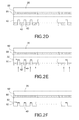
As shown in FIG. 2D, after the backside polishing, a photoresist pattern 42 is formed on the bottom face of the N type substrate 10 and the photoresist pattern 42 is used as mask to etch a plurality of trenches 40 on the back side of the N type substrate 10. Namely, the backside portion of the N type substrate 10, which is not covered by the photoresist pattern 42, is etched to form the plurality of trenches 40. Moreover, each of the trenches 40 has a trench depth and the trench depth is larger than 1 micrometer. As shown in FIG. 2E, after forming the trenches 40, the photoresist pattern 42 is used as mask for ion implantation and an ion implantation process is performed on the back side of the N type substrate 10 to form an N type ion implantation pattern 32. The N type ion implantation pattern 32 is formed on the bottom faces of the trenches, which are not covered by the photoresist pattern 42. Therefore, the N type ion implantation pattern 32 is separated with the bottom face of the N type substrate 10 by the trench depth larger than 1 micrometer.
As shown in FIGS. 2F and 2G, after removing the photoresist pattern 42, another ion implantation process is performed on the back side of the N type substrate 10 to form a P type ion implantation layer 34 on the remaining bottom face of the N type substrate 10. As shown in FIG. 2H, still another ion implantation process is performed on the back side of the N type substrate 10 to form an N type field stop ion implantation layer 36 on the back side of the N type substrate 10. Moreover, the N type field stop ion implantation layer 36 is separated with the bottom face of the N type substrate 10 by a field stop depth, where the field stop depth is larger than the trench depth. In other word, the N type field stop ion implantation layer 36 is deeper than the N type ion implantation pattern 32 to provide field stop function.
In the second embodiment, the N type field stop ion implantation layer 36 is formed after the trenches 40 are defined. Therefore, the N type field stop ion implantation layer 36 in the second embodiment has more fluctuated profile in comparison with the N type field stop ion implantation layer 30 in the first embodiment.
As shown in FIGS. 21 and 2J, after removing the protection layer 20, cleaning process with DHF and thermal annealing process are performed to form N type field stop doping region 36′, N type doping region 32′ and P type doping region 34′, respectively.
As shown in FIGS. 2K and 2L, after the thermal annealing process, emitter metal layer 50 and gate metal layer 51 are formed on top side of the N type substrate 10. Moreover, collector metal layer 52 is formed on bottom side of the N type substrate 10. The emitter metal layer 50, the gate metal layer 51 and the collector metal layer 52 can be formed by sputtering process, and the material of the emitter metal layer 50, the gate metal layer 51 and the collector metal layer 52 can be, but not limited to, aluminum (Al), TiN or tungsten (W).
As shown in FIG. 2L, the bottom side of the N type substrate 10 is formed with the plurality of the trenches 40 with trench depth larger than 1 micrometer. Moreover, the N type doping region 32′ is formed on the bottom of the trenches 40 such that the N type doping region 32′ has sufficient separation with the P type doping region 34′ along the depth direction. Therefore, the PN junction at the back side of the N type substrate 10 is irregular to prevent the Zener diode from forming and to enhance the performance of the IGBT device. Moreover, the N type field stop doping region 36′ also has fluctuated profile to further prevent the forming of the Zener diode.
The present invention is descried with above mentioned embodiment. However, the skilled in the related art can easily know the present invention has additional variations and embodiments. For example, the N type substrate 10 can be replaced with P type substrate, and the original N type doping is replaced by P type doping. Similarly the original P type doping is replaced by N type doping. This kind of variation can still have the effect to prevent the forming of the Zener diode.
Although the present invention has been described with reference to the preferred embodiment thereof, it will be understood that the invention is not limited to the details thereof. Various substitutions and modifications have suggested in the foregoing description, and other will occur to those of ordinary skill in the art. Therefore, all such substitutions and modifications are intended to be embraced within the scope of the invention as defined in the appended claims.

Claims (12)

What is claimed is:
1. A high-performance reverse-conduction field-stop (RCFS) insulated gate bipolar transistor (IGBT), comprising:
a first conductive type substrate;
a plurality of trenches defined on a bottom face of the first conductive type substrate;
a plurality of first conductive type doping regions formed on bottom faces of the trenches;
a second conductive type doping region formed on the bottom face of the first conductive type substrate; and
a first conductive type field stop doping region formed in the first conductive type substrate and separated with the bottom face of the first conductive type substrate with a field stop depth, where the field stop depth is larger than a depth of the trench, wherein the first conductive type is either N type or P type, and the second conductive type is either P type or N type correspondingly.
2. The high-performance RCFS IGBT in claim 1, wherein the first conductive type field stop doping region has fluctuated profile.
3. The high-performance RCFS IGBT in claim 1, wherein the trench depth is larger than 1 micrometer.
4. The high-performance RCFS IGBT in claim 1, further comprising: emitter metal layer and gate metal layer on front side of the first conductive type substrate, and collector metal layer on back side of the first conductive type substrate.
5. A method for manufacturing the high-performance reverse-conduction field-stop (RCFS) insulated gate bipolar transistor (IGBT) of claim 1, comprising:
(a) providing a first conductive type substrate and manufacturing a semi-finished semiconductor device on a front side of the substrate;
(b) covering a front side of the semiconductor device with a protection layer;
(c) performing an ion implantation process on back side of the first conductive type substrate to form a first conductive type field stop ion implantation with a field stop depth from a back face of the first conductive type substrate;
(d) forming a plurality of trenches on the back side of the first conductive type substrate, each of the trenches having a trench depth smaller than the field stop depth;
(e) performing an ion implantation process on back side of the first conductive type substrate to form a first conductive type ion implantation pattern on bottom faces of the trenches; and
(f) performing an ion implantation process on back side of the first conductive type substrate to form a second conductive type ion implantation layer on back face of the first conductive type substrate,
wherein the first conductive type is either N type or P type, and the second conductive type is either P type or N type correspondingly.
6. The method for manufacturing a high-performance RCFS IGBT in claim 5, further comprising: after step (b), removing part of back side of the first conductive type substrate.
7. The method for manufacturing a high-performance RCFS IGBT in claim 5, further comprising: after step (f), performing thermal annealing process to form first conductive type field stop doping region, first conductive type doping region, and second conductive type doping region, respectively.
8. The method for manufacturing a high-performance RCFS IGBT in claim 5, wherein the trench depth is larger than 1 micrometer.
9. A method for manufacturing the high-performance reverse-conduction field-stop (RCFS) insulated gate bipolar transistor (IGBT) of claim 1, comprising:
(a) providing a first conductive type substrate and manufacturing a semi-finished semiconductor device on a front side of the substrate;
(b) covering a front side of the semiconductor device with a protection layer;
(c) forming a plurality of trenches on the back side of the first conductive type substrate, each of the trenches having a trench depth;
(d) performing an ion implantation process on back side of the first conductive type substrate to form a first conductive type ion implantation pattern on bottom faces of the trenches;
(e) performing an ion implantation process on back side of the first conductive type substrate to form a second conductive type ion implantation layer on back face of the first conductive type substrate; and
(f) performing an ion implantation process on back side of the first conductive type substrate to form a first conductive type field stop ion implantation with a field stop depth from back face of the first conductive type substrate, where the trench depth is smaller than the field stop depth,
wherein the first conductive type is either N type or P type, and the second conductive type is either P type or N type correspondingly.
10. The method for manufacturing a high-performance RCFS IGBT in claim 9, further comprising: after step (b), removing part of back side of the first conductive type substrate.
11. The method for manufacturing a high-performance I RCFS GBT in claim 9, further comprising: after step (f), performing thermal annealing process to form first conductive type field stop doping region, first conductive type doping region, and second conductive type doping region, respectively.
12. The method for manufacturing a high-performance RCFS IGBT in claim 9, wherein the trench depth is larger than 1 micrometer.
US14/526,090 2014-03-31 2014-10-28 High-performance reverse-conduction field-stop (RCFS) insulated gate bipolar transistor and method for manufacturing the same Active US9240470B2 (en)

Applications Claiming Priority (3)

Application Number Priority Date Filing Date Title
TW103112038 2014-03-31
TW103112038A TWI534911B (en) 2014-03-31 2014-03-31 High-performance insulated gate bipolar transistor (igbt) and method for making the same
TW103112038A 2014-03-31

Publications (2)

Publication Number Publication Date
US20150279980A1 US20150279980A1 (en) 2015-10-01
US9240470B2 true US9240470B2 (en) 2016-01-19

Family

ID=54191533

Family Applications (1)

Application Number Title Priority Date Filing Date
US14/526,090 Active US9240470B2 (en) 2014-03-31 2014-10-28 High-performance reverse-conduction field-stop (RCFS) insulated gate bipolar transistor and method for manufacturing the same

Country Status (2)

Country Link
US (1) US9240470B2 (en)
TW (1) TWI534911B (en)

Families Citing this family (4)

* Cited by examiner, † Cited by third party
Publication number Priority date Publication date Assignee Title
CN107359198A (en) * 2017-08-14 2017-11-17 深圳市芯电元科技有限公司 Novel anode short circuit type IGBT and preparation method thereof
TWI695418B (en) * 2017-09-22 2020-06-01 新唐科技股份有限公司 Semiconductor device and method of manufacturing the same
US10546948B1 (en) 2018-09-11 2020-01-28 Semiconductor Components Industries, Llc Electronic device including an insulated gate bipolar transistor having a field-stop region and a process of forming the same
CN109473355A (en) * 2018-10-12 2019-03-15 龙腾半导体有限公司 Enhance the method for inverse conductivity type IGBT avalanche capability

Citations (4)

* Cited by examiner, † Cited by third party
Publication number Priority date Publication date Assignee Title
US20130134478A1 (en) * 2011-10-17 2013-05-30 Rohm Co., Ltd. Semiconductor device and method for manufacturing same
US20140295625A1 (en) * 2011-06-08 2014-10-02 Rohm Co., Ltd. Manufacturing method of semiconductor device
US20140312382A1 (en) * 2012-04-24 2014-10-23 Fairchild Korea Semiconductor Ltd. Power device and method of manufacturing the same
US20150162418A1 (en) * 2013-12-10 2015-06-11 Infineon Technologies Ag Method for forming a semiconductor device

Patent Citations (4)

* Cited by examiner, † Cited by third party
Publication number Priority date Publication date Assignee Title
US20140295625A1 (en) * 2011-06-08 2014-10-02 Rohm Co., Ltd. Manufacturing method of semiconductor device
US20130134478A1 (en) * 2011-10-17 2013-05-30 Rohm Co., Ltd. Semiconductor device and method for manufacturing same
US20140312382A1 (en) * 2012-04-24 2014-10-23 Fairchild Korea Semiconductor Ltd. Power device and method of manufacturing the same
US20150162418A1 (en) * 2013-12-10 2015-06-11 Infineon Technologies Ag Method for forming a semiconductor device

Also Published As

Publication number Publication date
TWI534911B (en) 2016-05-21
US20150279980A1 (en) 2015-10-01
TW201537641A (en) 2015-10-01

Similar Documents

Publication Publication Date Title
US8242537B2 (en) IGBT with fast reverse recovery time rectifier and manufacturing method thereof
US10580769B2 (en) Semiconductor device with schottky diode and manufacturing method thereof
EP1239522A2 (en) Semiconductor device having insulated gate bipolar transistor with dielectric isolation structure and method of manufacturing the same
US9240470B2 (en) High-performance reverse-conduction field-stop (RCFS) insulated gate bipolar transistor and method for manufacturing the same
TWI415173B (en) Method for fabricating a super junction power device with reduced miller capacitance
US8809946B2 (en) Wide trench termination structure for semiconductor device
US8735973B2 (en) Trench-gate MOSFET device and method for making the same
EP3723137A1 (en) Diode structure and manufacturing method thereof
US20160293745A1 (en) Power semiconductor device and fabrication method thereof
US9012955B2 (en) MOS transistor on SOI protected against overvoltages
JP2011176027A (en) Semiconductor element and method of manufacturing the same
EP3474330B1 (en) Lateral insulated-gate bipolar transistor and manufacturing method therefor
US20130234237A1 (en) Semiconductor power device integrated with clamp diodes having dopant out-diffusion suppression layers
US20150364562A1 (en) Semiconductor device
KR20170051122A (en) Semiconductor structure
US10490629B2 (en) Method for fabricating power semiconductor device
US20150137230A1 (en) Laterally diffused metal oxide semiconductor and manufacturing method thereof
US20160211258A1 (en) Reverse-Conducting Gated-Base Bipolar-Conduction Devices and Methods with Reduced Risk of Warping
US20170170310A1 (en) Semiconductor device and manufacturing method of the semiconductor device
JP2011176026A (en) Method of manufacturing semiconductor element
US20130234238A1 (en) Semiconductor power device integrated with esd protection diodes
US9105757B2 (en) Junction barrier Schottky diode and manufacturing method thereof
JP2017045874A (en) Semiconductor device
US11257720B2 (en) Manufacturing method for semiconductor device and integrated semiconductor device
CN109148606B (en) High voltage element

Legal Events

Date Code Title Description
AS Assignment

Owner name: PFC DEVICE HOLDINGS LIMITED, TAIWAN

Free format text: ASSIGNMENT OF ASSIGNORS INTEREST;ASSIGNORS:CHEN, MEI-LING;KUO, HUNG-HSIN;HSIA, YI-LUN;AND OTHERS;SIGNING DATES FROM 20140422 TO 20141014;REEL/FRAME:034071/0540

STCF Information on status: patent grant

Free format text: PATENTED CASE

MAFP Maintenance fee payment

Free format text: PAYMENT OF MAINTENANCE FEE, 4TH YR, SMALL ENTITY (ORIGINAL EVENT CODE: M2551); ENTITY STATUS OF PATENT OWNER: SMALL ENTITY

Year of fee payment: 4

MAFP Maintenance fee payment

Free format text: PAYMENT OF MAINTENANCE FEE, 8TH YR, SMALL ENTITY (ORIGINAL EVENT CODE: M2552); ENTITY STATUS OF PATENT OWNER: SMALL ENTITY

Year of fee payment: 8