US9236312B2 - Preventing EPI damage for cap nitride strip scheme in a Fin-shaped field effect transistor (FinFET) device - Google Patents
Preventing EPI damage for cap nitride strip scheme in a Fin-shaped field effect transistor (FinFET) device Download PDFInfo
- Publication number
- US9236312B2 US9236312B2 US14/053,088 US201314053088A US9236312B2 US 9236312 B2 US9236312 B2 US 9236312B2 US 201314053088 A US201314053088 A US 201314053088A US 9236312 B2 US9236312 B2 US 9236312B2
- Authority
- US
- United States
- Prior art keywords
- forming
- rsd
- structures
- regions
- capping layer
- Prior art date
- Legal status (The legal status is an assumption and is not a legal conclusion. Google has not performed a legal analysis and makes no representation as to the accuracy of the status listed.)
- Active, expires
Links
- 150000004767 nitrides Chemical class 0.000 title claims abstract description 38
- 230000005669 field effect Effects 0.000 title claims abstract description 8
- 238000000034 method Methods 0.000 claims abstract description 64
- 230000008569 process Effects 0.000 claims abstract description 32
- OAICVXFJPJFONN-UHFFFAOYSA-N Phosphorus Chemical compound [P] OAICVXFJPJFONN-UHFFFAOYSA-N 0.000 claims abstract description 11
- 229910052698 phosphorus Inorganic materials 0.000 claims abstract description 11
- 239000011574 phosphorus Substances 0.000 claims abstract description 11
- 239000000758 substrate Substances 0.000 claims description 35
- BPQQTUXANYXVAA-UHFFFAOYSA-N Orthosilicate Chemical compound [O-][Si]([O-])([O-])[O-] BPQQTUXANYXVAA-UHFFFAOYSA-N 0.000 claims description 21
- 230000003647 oxidation Effects 0.000 claims description 14
- 238000007254 oxidation reaction Methods 0.000 claims description 14
- 229910000577 Silicon-germanium Inorganic materials 0.000 claims description 13
- 230000001590 oxidative effect Effects 0.000 claims description 8
- LEVVHYCKPQWKOP-UHFFFAOYSA-N [Si].[Ge] Chemical compound [Si].[Ge] LEVVHYCKPQWKOP-UHFFFAOYSA-N 0.000 claims description 5
- 239000004065 semiconductor Substances 0.000 abstract description 20
- 125000006850 spacer group Chemical group 0.000 abstract description 8
- 238000013459 approach Methods 0.000 abstract description 6
- 238000012545 processing Methods 0.000 abstract description 5
- 239000010410 layer Substances 0.000 description 44
- XUIMIQQOPSSXEZ-UHFFFAOYSA-N Silicon Chemical compound [Si] XUIMIQQOPSSXEZ-UHFFFAOYSA-N 0.000 description 12
- 229910052710 silicon Inorganic materials 0.000 description 12
- 239000010703 silicon Substances 0.000 description 12
- 230000015572 biosynthetic process Effects 0.000 description 11
- 238000005229 chemical vapour deposition Methods 0.000 description 9
- 238000000151 deposition Methods 0.000 description 7
- 230000008021 deposition Effects 0.000 description 6
- 239000000463 material Substances 0.000 description 5
- VYPSYNLAJGMNEJ-UHFFFAOYSA-N Silicium dioxide Chemical compound O=[Si]=O VYPSYNLAJGMNEJ-UHFFFAOYSA-N 0.000 description 4
- 238000000226 double patterning lithography Methods 0.000 description 4
- 230000000694 effects Effects 0.000 description 4
- 238000004518 low pressure chemical vapour deposition Methods 0.000 description 4
- 238000000206 photolithography Methods 0.000 description 4
- 238000005240 physical vapour deposition Methods 0.000 description 4
- 238000000623 plasma-assisted chemical vapour deposition Methods 0.000 description 4
- 238000013461 design Methods 0.000 description 3
- 238000005530 etching Methods 0.000 description 3
- 230000000873 masking effect Effects 0.000 description 3
- 229910052581 Si3N4 Inorganic materials 0.000 description 2
- 238000001505 atmospheric-pressure chemical vapour deposition Methods 0.000 description 2
- 238000000277 atomic layer chemical vapour deposition Methods 0.000 description 2
- 238000000231 atomic layer deposition Methods 0.000 description 2
- 239000000969 carrier Substances 0.000 description 2
- 238000006243 chemical reaction Methods 0.000 description 2
- 229910052735 hafnium Inorganic materials 0.000 description 2
- VBJZVLUMGGDVMO-UHFFFAOYSA-N hafnium atom Chemical compound [Hf] VBJZVLUMGGDVMO-UHFFFAOYSA-N 0.000 description 2
- 238000012986 modification Methods 0.000 description 2
- 230000004048 modification Effects 0.000 description 2
- 238000005268 plasma chemical vapour deposition Methods 0.000 description 2
- 238000001289 rapid thermal chemical vapour deposition Methods 0.000 description 2
- HQVNEWCFYHHQES-UHFFFAOYSA-N silicon nitride Chemical compound N12[Si]34N5[Si]62N3[Si]51N64 HQVNEWCFYHHQES-UHFFFAOYSA-N 0.000 description 2
- 229910052814 silicon oxide Inorganic materials 0.000 description 2
- 239000000126 substance Substances 0.000 description 2
- 238000000038 ultrahigh vacuum chemical vapour deposition Methods 0.000 description 2
- 229910019001 CoSi Inorganic materials 0.000 description 1
- 229910005883 NiSi Inorganic materials 0.000 description 1
- 229910004166 TaN Inorganic materials 0.000 description 1
- ATJFFYVFTNAWJD-UHFFFAOYSA-N Tin Chemical compound [Sn] ATJFFYVFTNAWJD-UHFFFAOYSA-N 0.000 description 1
- 229910045601 alloy Inorganic materials 0.000 description 1
- 239000000956 alloy Substances 0.000 description 1
- PNEYBMLMFCGWSK-UHFFFAOYSA-N aluminium oxide Inorganic materials [O-2].[O-2].[O-2].[Al+3].[Al+3] PNEYBMLMFCGWSK-UHFFFAOYSA-N 0.000 description 1
- 230000004888 barrier function Effects 0.000 description 1
- 229910052681 coesite Inorganic materials 0.000 description 1
- 230000000295 complement effect Effects 0.000 description 1
- 239000004020 conductor Substances 0.000 description 1
- 229910052802 copper Inorganic materials 0.000 description 1
- 229910052906 cristobalite Inorganic materials 0.000 description 1
- 239000003989 dielectric material Substances 0.000 description 1
- 238000000313 electron-beam-induced deposition Methods 0.000 description 1
- 238000005516 engineering process Methods 0.000 description 1
- 238000001704 evaporation Methods 0.000 description 1
- 230000008020 evaporation Effects 0.000 description 1
- 230000006870 function Effects 0.000 description 1
- 229910000449 hafnium oxide Inorganic materials 0.000 description 1
- WIHZLLGSGQNAGK-UHFFFAOYSA-N hafnium(4+);oxygen(2-) Chemical compound [O-2].[O-2].[Hf+4] WIHZLLGSGQNAGK-UHFFFAOYSA-N 0.000 description 1
- 238000011065 in-situ storage Methods 0.000 description 1
- 239000012212 insulator Substances 0.000 description 1
- 238000007737 ion beam deposition Methods 0.000 description 1
- 150000002500 ions Chemical class 0.000 description 1
- 238000001459 lithography Methods 0.000 description 1
- 238000004519 manufacturing process Methods 0.000 description 1
- 230000007246 mechanism Effects 0.000 description 1
- 229910052751 metal Inorganic materials 0.000 description 1
- 239000002184 metal Substances 0.000 description 1
- 150000002736 metal compounds Chemical class 0.000 description 1
- 238000001451 molecular beam epitaxy Methods 0.000 description 1
- 229910052750 molybdenum Inorganic materials 0.000 description 1
- TWNQGVIAIRXVLR-UHFFFAOYSA-N oxo(oxoalumanyloxy)alumane Chemical compound O=[Al]O[Al]=O TWNQGVIAIRXVLR-UHFFFAOYSA-N 0.000 description 1
- RVTZCBVAJQQJTK-UHFFFAOYSA-N oxygen(2-);zirconium(4+) Chemical compound [O-2].[O-2].[Zr+4] RVTZCBVAJQQJTK-UHFFFAOYSA-N 0.000 description 1
- 238000000059 patterning Methods 0.000 description 1
- 229920002120 photoresistant polymer Polymers 0.000 description 1
- 238000007747 plating Methods 0.000 description 1
- 238000005498 polishing Methods 0.000 description 1
- 229920000747 poly(lactic acid) Polymers 0.000 description 1
- 229910021420 polycrystalline silicon Inorganic materials 0.000 description 1
- 229920005591 polysilicon Polymers 0.000 description 1
- 239000000377 silicon dioxide Substances 0.000 description 1
- 235000012239 silicon dioxide Nutrition 0.000 description 1
- 238000004544 sputter deposition Methods 0.000 description 1
- 229910052682 stishovite Inorganic materials 0.000 description 1
- 239000002344 surface layer Substances 0.000 description 1
- 229910052715 tantalum Inorganic materials 0.000 description 1
- 229910052718 tin Inorganic materials 0.000 description 1
- 229910052719 titanium Inorganic materials 0.000 description 1
- 229910052905 tridymite Inorganic materials 0.000 description 1
- 229910052721 tungsten Inorganic materials 0.000 description 1
- 229910001928 zirconium oxide Inorganic materials 0.000 description 1
Images


Classifications
-
- H—ELECTRICITY
- H01—ELECTRIC ELEMENTS
- H01L—SEMICONDUCTOR DEVICES NOT COVERED BY CLASS H10
- H01L27/00—Devices consisting of a plurality of semiconductor or other solid-state components formed in or on a common substrate
- H01L27/02—Devices consisting of a plurality of semiconductor or other solid-state components formed in or on a common substrate including semiconductor components specially adapted for rectifying, oscillating, amplifying or switching and having at least one potential-jump barrier or surface barrier; including integrated passive circuit elements with at least one potential-jump barrier or surface barrier
- H01L27/04—Devices consisting of a plurality of semiconductor or other solid-state components formed in or on a common substrate including semiconductor components specially adapted for rectifying, oscillating, amplifying or switching and having at least one potential-jump barrier or surface barrier; including integrated passive circuit elements with at least one potential-jump barrier or surface barrier the substrate being a semiconductor body
- H01L27/08—Devices consisting of a plurality of semiconductor or other solid-state components formed in or on a common substrate including semiconductor components specially adapted for rectifying, oscillating, amplifying or switching and having at least one potential-jump barrier or surface barrier; including integrated passive circuit elements with at least one potential-jump barrier or surface barrier the substrate being a semiconductor body including only semiconductor components of a single kind
- H01L27/085—Devices consisting of a plurality of semiconductor or other solid-state components formed in or on a common substrate including semiconductor components specially adapted for rectifying, oscillating, amplifying or switching and having at least one potential-jump barrier or surface barrier; including integrated passive circuit elements with at least one potential-jump barrier or surface barrier the substrate being a semiconductor body including only semiconductor components of a single kind including field-effect components only
- H01L27/088—Devices consisting of a plurality of semiconductor or other solid-state components formed in or on a common substrate including semiconductor components specially adapted for rectifying, oscillating, amplifying or switching and having at least one potential-jump barrier or surface barrier; including integrated passive circuit elements with at least one potential-jump barrier or surface barrier the substrate being a semiconductor body including only semiconductor components of a single kind including field-effect components only the components being field-effect transistors with insulated gate
- H01L27/092—Devices consisting of a plurality of semiconductor or other solid-state components formed in or on a common substrate including semiconductor components specially adapted for rectifying, oscillating, amplifying or switching and having at least one potential-jump barrier or surface barrier; including integrated passive circuit elements with at least one potential-jump barrier or surface barrier the substrate being a semiconductor body including only semiconductor components of a single kind including field-effect components only the components being field-effect transistors with insulated gate complementary MIS field-effect transistors
- H01L27/0924—Devices consisting of a plurality of semiconductor or other solid-state components formed in or on a common substrate including semiconductor components specially adapted for rectifying, oscillating, amplifying or switching and having at least one potential-jump barrier or surface barrier; including integrated passive circuit elements with at least one potential-jump barrier or surface barrier the substrate being a semiconductor body including only semiconductor components of a single kind including field-effect components only the components being field-effect transistors with insulated gate complementary MIS field-effect transistors including transistors with a horizontal current flow in a vertical sidewall of a semiconductor body, e.g. FinFET, MuGFET
-
- H—ELECTRICITY
- H01—ELECTRIC ELEMENTS
- H01L—SEMICONDUCTOR DEVICES NOT COVERED BY CLASS H10
- H01L21/00—Processes or apparatus adapted for the manufacture or treatment of semiconductor or solid state devices or of parts thereof
- H01L21/70—Manufacture or treatment of devices consisting of a plurality of solid state components formed in or on a common substrate or of parts thereof; Manufacture of integrated circuit devices or of parts thereof
- H01L21/71—Manufacture of specific parts of devices defined in group H01L21/70
- H01L21/76—Making of isolation regions between components
- H01L21/762—Dielectric regions, e.g. EPIC dielectric isolation, LOCOS; Trench refilling techniques, SOI technology, use of channel stoppers
- H01L21/76224—Dielectric regions, e.g. EPIC dielectric isolation, LOCOS; Trench refilling techniques, SOI technology, use of channel stoppers using trench refilling with dielectric materials
-
- H—ELECTRICITY
- H01—ELECTRIC ELEMENTS
- H01L—SEMICONDUCTOR DEVICES NOT COVERED BY CLASS H10
- H01L21/00—Processes or apparatus adapted for the manufacture or treatment of semiconductor or solid state devices or of parts thereof
- H01L21/70—Manufacture or treatment of devices consisting of a plurality of solid state components formed in or on a common substrate or of parts thereof; Manufacture of integrated circuit devices or of parts thereof
- H01L21/77—Manufacture or treatment of devices consisting of a plurality of solid state components or integrated circuits formed in, or on, a common substrate
- H01L21/78—Manufacture or treatment of devices consisting of a plurality of solid state components or integrated circuits formed in, or on, a common substrate with subsequent division of the substrate into plural individual devices
- H01L21/82—Manufacture or treatment of devices consisting of a plurality of solid state components or integrated circuits formed in, or on, a common substrate with subsequent division of the substrate into plural individual devices to produce devices, e.g. integrated circuits, each consisting of a plurality of components
- H01L21/822—Manufacture or treatment of devices consisting of a plurality of solid state components or integrated circuits formed in, or on, a common substrate with subsequent division of the substrate into plural individual devices to produce devices, e.g. integrated circuits, each consisting of a plurality of components the substrate being a semiconductor, using silicon technology
- H01L21/8232—Field-effect technology
- H01L21/8234—MIS technology, i.e. integration processes of field effect transistors of the conductor-insulator-semiconductor type
- H01L21/8238—Complementary field-effect transistors, e.g. CMOS
- H01L21/823814—Complementary field-effect transistors, e.g. CMOS with a particular manufacturing method of the source or drain structures, e.g. specific source or drain implants or silicided source or drain structures or raised source or drain structures
-
- H—ELECTRICITY
- H01—ELECTRIC ELEMENTS
- H01L—SEMICONDUCTOR DEVICES NOT COVERED BY CLASS H10
- H01L21/00—Processes or apparatus adapted for the manufacture or treatment of semiconductor or solid state devices or of parts thereof
- H01L21/70—Manufacture or treatment of devices consisting of a plurality of solid state components formed in or on a common substrate or of parts thereof; Manufacture of integrated circuit devices or of parts thereof
- H01L21/77—Manufacture or treatment of devices consisting of a plurality of solid state components or integrated circuits formed in, or on, a common substrate
- H01L21/78—Manufacture or treatment of devices consisting of a plurality of solid state components or integrated circuits formed in, or on, a common substrate with subsequent division of the substrate into plural individual devices
- H01L21/82—Manufacture or treatment of devices consisting of a plurality of solid state components or integrated circuits formed in, or on, a common substrate with subsequent division of the substrate into plural individual devices to produce devices, e.g. integrated circuits, each consisting of a plurality of components
- H01L21/822—Manufacture or treatment of devices consisting of a plurality of solid state components or integrated circuits formed in, or on, a common substrate with subsequent division of the substrate into plural individual devices to produce devices, e.g. integrated circuits, each consisting of a plurality of components the substrate being a semiconductor, using silicon technology
- H01L21/8232—Field-effect technology
- H01L21/8234—MIS technology, i.e. integration processes of field effect transistors of the conductor-insulator-semiconductor type
- H01L21/8238—Complementary field-effect transistors, e.g. CMOS
- H01L21/823821—Complementary field-effect transistors, e.g. CMOS with a particular manufacturing method of transistors with a horizontal current flow in a vertical sidewall of a semiconductor body, e.g. FinFET, MuGFET
-
- H—ELECTRICITY
- H01—ELECTRIC ELEMENTS
- H01L—SEMICONDUCTOR DEVICES NOT COVERED BY CLASS H10
- H01L27/00—Devices consisting of a plurality of semiconductor or other solid-state components formed in or on a common substrate
- H01L27/02—Devices consisting of a plurality of semiconductor or other solid-state components formed in or on a common substrate including semiconductor components specially adapted for rectifying, oscillating, amplifying or switching and having at least one potential-jump barrier or surface barrier; including integrated passive circuit elements with at least one potential-jump barrier or surface barrier
- H01L27/04—Devices consisting of a plurality of semiconductor or other solid-state components formed in or on a common substrate including semiconductor components specially adapted for rectifying, oscillating, amplifying or switching and having at least one potential-jump barrier or surface barrier; including integrated passive circuit elements with at least one potential-jump barrier or surface barrier the substrate being a semiconductor body
- H01L27/08—Devices consisting of a plurality of semiconductor or other solid-state components formed in or on a common substrate including semiconductor components specially adapted for rectifying, oscillating, amplifying or switching and having at least one potential-jump barrier or surface barrier; including integrated passive circuit elements with at least one potential-jump barrier or surface barrier the substrate being a semiconductor body including only semiconductor components of a single kind
- H01L27/085—Devices consisting of a plurality of semiconductor or other solid-state components formed in or on a common substrate including semiconductor components specially adapted for rectifying, oscillating, amplifying or switching and having at least one potential-jump barrier or surface barrier; including integrated passive circuit elements with at least one potential-jump barrier or surface barrier the substrate being a semiconductor body including only semiconductor components of a single kind including field-effect components only
- H01L27/088—Devices consisting of a plurality of semiconductor or other solid-state components formed in or on a common substrate including semiconductor components specially adapted for rectifying, oscillating, amplifying or switching and having at least one potential-jump barrier or surface barrier; including integrated passive circuit elements with at least one potential-jump barrier or surface barrier the substrate being a semiconductor body including only semiconductor components of a single kind including field-effect components only the components being field-effect transistors with insulated gate
- H01L27/0886—Devices consisting of a plurality of semiconductor or other solid-state components formed in or on a common substrate including semiconductor components specially adapted for rectifying, oscillating, amplifying or switching and having at least one potential-jump barrier or surface barrier; including integrated passive circuit elements with at least one potential-jump barrier or surface barrier the substrate being a semiconductor body including only semiconductor components of a single kind including field-effect components only the components being field-effect transistors with insulated gate including transistors with a horizontal current flow in a vertical sidewall of a semiconductor body, e.g. FinFET, MuGFET
-
- H—ELECTRICITY
- H01—ELECTRIC ELEMENTS
- H01L—SEMICONDUCTOR DEVICES NOT COVERED BY CLASS H10
- H01L29/00—Semiconductor devices adapted for rectifying, amplifying, oscillating or switching, or capacitors or resistors with at least one potential-jump barrier or surface barrier, e.g. PN junction depletion layer or carrier concentration layer; Details of semiconductor bodies or of electrodes thereof ; Multistep manufacturing processes therefor
- H01L29/02—Semiconductor bodies ; Multistep manufacturing processes therefor
- H01L29/12—Semiconductor bodies ; Multistep manufacturing processes therefor characterised by the materials of which they are formed
- H01L29/16—Semiconductor bodies ; Multistep manufacturing processes therefor characterised by the materials of which they are formed including, apart from doping materials or other impurities, only elements of Group IV of the Periodic System
- H01L29/161—Semiconductor bodies ; Multistep manufacturing processes therefor characterised by the materials of which they are formed including, apart from doping materials or other impurities, only elements of Group IV of the Periodic System including two or more of the elements provided for in group H01L29/16, e.g. alloys
-
- H—ELECTRICITY
- H01—ELECTRIC ELEMENTS
- H01L—SEMICONDUCTOR DEVICES NOT COVERED BY CLASS H10
- H01L29/00—Semiconductor devices adapted for rectifying, amplifying, oscillating or switching, or capacitors or resistors with at least one potential-jump barrier or surface barrier, e.g. PN junction depletion layer or carrier concentration layer; Details of semiconductor bodies or of electrodes thereof ; Multistep manufacturing processes therefor
- H01L29/02—Semiconductor bodies ; Multistep manufacturing processes therefor
- H01L29/12—Semiconductor bodies ; Multistep manufacturing processes therefor characterised by the materials of which they are formed
- H01L29/16—Semiconductor bodies ; Multistep manufacturing processes therefor characterised by the materials of which they are formed including, apart from doping materials or other impurities, only elements of Group IV of the Periodic System
- H01L29/167—Semiconductor bodies ; Multistep manufacturing processes therefor characterised by the materials of which they are formed including, apart from doping materials or other impurities, only elements of Group IV of the Periodic System further characterised by the doping material
-
- H—ELECTRICITY
- H01—ELECTRIC ELEMENTS
- H01L—SEMICONDUCTOR DEVICES NOT COVERED BY CLASS H10
- H01L29/00—Semiconductor devices adapted for rectifying, amplifying, oscillating or switching, or capacitors or resistors with at least one potential-jump barrier or surface barrier, e.g. PN junction depletion layer or carrier concentration layer; Details of semiconductor bodies or of electrodes thereof ; Multistep manufacturing processes therefor
- H01L29/40—Electrodes ; Multistep manufacturing processes therefor
- H01L29/41—Electrodes ; Multistep manufacturing processes therefor characterised by their shape, relative sizes or dispositions
- H01L29/417—Electrodes ; Multistep manufacturing processes therefor characterised by their shape, relative sizes or dispositions carrying the current to be rectified, amplified or switched
- H01L29/41725—Source or drain electrodes for field effect devices
- H01L29/41775—Source or drain electrodes for field effect devices characterised by the proximity or the relative position of the source or drain electrode and the gate electrode, e.g. the source or drain electrode separated from the gate electrode by side-walls or spreading around or above the gate electrode
- H01L29/41783—Raised source or drain electrodes self aligned with the gate
-
- H—ELECTRICITY
- H01—ELECTRIC ELEMENTS
- H01L—SEMICONDUCTOR DEVICES NOT COVERED BY CLASS H10
- H01L29/00—Semiconductor devices adapted for rectifying, amplifying, oscillating or switching, or capacitors or resistors with at least one potential-jump barrier or surface barrier, e.g. PN junction depletion layer or carrier concentration layer; Details of semiconductor bodies or of electrodes thereof ; Multistep manufacturing processes therefor
- H01L29/66—Types of semiconductor device ; Multistep manufacturing processes therefor
- H01L29/66007—Multistep manufacturing processes
- H01L29/66075—Multistep manufacturing processes of devices having semiconductor bodies comprising group 14 or group 13/15 materials
- H01L29/66227—Multistep manufacturing processes of devices having semiconductor bodies comprising group 14 or group 13/15 materials the devices being controllable only by the electric current supplied or the electric potential applied, to an electrode which does not carry the current to be rectified, amplified or switched, e.g. three-terminal devices
- H01L29/66409—Unipolar field-effect transistors
- H01L29/66477—Unipolar field-effect transistors with an insulated gate, i.e. MISFET
- H01L29/66787—Unipolar field-effect transistors with an insulated gate, i.e. MISFET with a gate at the side of the channel
- H01L29/66795—Unipolar field-effect transistors with an insulated gate, i.e. MISFET with a gate at the side of the channel with a horizontal current flow in a vertical sidewall of a semiconductor body, e.g. FinFET, MuGFET
Definitions
- This invention relates generally to the field of semiconductors, and more particularly, to forming a nitride spacer to protect a FinFET device.
- a typical integrated circuit (IC) chip includes a stack of several levels or sequentially formed layers of shapes. Each layer is stacked or overlaid on a prior layer and patterned to form the shapes that define devices (e.g., field effect transistors (FETs)) and connect the devices into circuits.
- FETs field effect transistors
- CMOS complementary insulated gate FET process
- layers are formed on a wafer to form the devices on a surface of the wafer. Further, the surface may be the surface of a silicon layer on a silicon on insulator (SOI) wafer.
- SOI silicon on insulator
- a simple FET is formed by the intersection of two shapes, a gate layer rectangle on a silicon island formed from the silicon surface layer.
- Each of these layers of shapes also known as mask levels or layers, may be created or printed optically through well-known photolithographic masking, developing, and level definition (e.g., etching, implanting, deposition, etc.).
- the FinFET is a transistor design that attempts to overcome the issues of short-channel effect encountered by deep submicron transistors, such as drain-induced barrier lowering (DIBL). Such effects make it harder for the voltage on a gate electrode to deplete the channel underneath and stop the flow of carriers through the channel—in other words, to turn the transistor off.
- DIBL drain-induced barrier lowering
- approaches for forming an oxide cap to protect a semiconductor device are provided.
- a semiconductor device e.g., a fin field effect transistor device (FinFET)
- approaches are provided for forming an oxide cap over a subset (e.g., SiP regions) of raised source drain (RSD) structures on the set of fins of the FinFET device to mitigate damage during subsequent processing.
- the oxide spacer is deposited before the removal of a nitride capping layer from the FinFET device (e.g., by a hot phosphorus wash).
- the oxide cap on top of the RSD structures will be preserved throughout the removal of the nitride capping layer to provide hardmask protection during this process.
- One aspect of the present invention includes a method for forming a device, the method comprising: forming a set of gate structures over a finned substrate, each of the set of gate structures comprising a nitride capping layer; forming a set of raised source drain (RSD) structures on the finned substrate; forming an oxide cap over a subset of the RSD structures; and removing the nitride capping layer.
- a method for forming a device comprising: forming a set of gate structures over a finned substrate, each of the set of gate structures comprising a nitride capping layer; forming a set of raised source drain (RSD) structures on the finned substrate; forming an oxide cap over a subset of the RSD structures; and removing the nitride capping layer.
- RSD raised source drain
- Another aspect of the present invention includes a method for forming an oxide cap to protect a fin-shaped field effect transistor (FinFET) device, the method comprising: forming a set of gate structures over a finned substrate, each of the set of gate structures comprising a nitride capping layer; forming a set of raised source drain (RSD) structures on the finned substrate; forming a silicate over a subset of the RSD structures; oxidizing the silicate to form the oxide cap; and removing the nitride capping layer.
- FinFET fin-shaped field effect transistor
- Yet another aspect of the present invention includes a fin-shaped field effect transistor (FinFET) device, formed via a process, comprising: forming a set of fins from a substrate to get a finned substrate; forming a set of gate structures over the finned substrate, each of the set of gate structures comprising a nitride capping layer; growing a set of epitaxial phosphorus-doped Si (SiP) regions over a subset of the set of gate structures; growing a silicate on the SiP regions; oxidizing the silicate using a plasma oxidation process to form an oxide cap; removing the nitride capping layer via a hot phosphorus rinse, wherein the oxide cap prevents damage to the SiP regions from the hot phosphorus rinse; and removing the oxide cap from the SiP regions.
- FinFET fin-shaped field effect transistor
- FIG. 1 shows a FinFET semiconductor device according to an embodiment of the present invention
- FIG. 2 shows a “dummy” gate formation according to an embodiment of the present invention
- FIG. 3 shows a spacer formation according to an embodiment of the present invention
- FIG. 4 shows a nitride cap formation according to an embodiment of the present invention
- FIG. 5 shows a formation of raise source drain (RSD) structures according to an embodiment of the present invention
- FIG. 6 shows RSD structures having SiP and SiGe regions according to an embodiment of the present invention
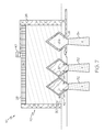
- FIG. 7 shows a formation of a silicate on the SiP regions according to an embodiment of the present invention.
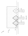
- FIG. 8 shows an oxidizing of the silicate to form an oxide cap according to an embodiment of the present invention.
- FIG. 9 shows a removal of a nitride capping layer according an embodiment of the present invention.
- approaches for forming an oxide cap to protect a semiconductor device e.g., a fin field effect transistor device (FinFET)
- a semiconductor device e.g., a fin field effect transistor device (FinFET)
- approaches are provided for forming an oxide cap over a subset (e.g., SiP regions) of raised source drain (RSD) structures on the set of fins of the FinFET device to mitigate damage during subsequent processing.
- the oxide spacer is deposited before the removal of a nitride capping layer from the FinFET device (e.g., by a hot phosphorus wash).
- the oxide cap on top of the RSD structures will be preserved throughout the removal of the nitride capping layer to provide hardmask protection during this process.
- first element such as a first structure, e.g., a first layer
- second element such as a second structure, e.g. a second layer
- intervening elements such as an interface structure, e.g. interface layer
- depositing may include any now known or later developed techniques appropriate for the material to be deposited including but not limited to, for example: chemical vapor deposition (CVD), low-pressure CVD (LPCVD), plasma-enhanced CVD (PECVD), semi-atmosphere CVD (SACVD) and high density plasma CVD (HDPCVD), rapid thermal CVD (RTCVD), ultra-high vacuum CVD (UHVCVD), limited reaction processing CVD (LRPCVD), metal-organic CVD (MOCVD), sputtering deposition, ion beam deposition, electron beam deposition, laser assisted deposition, thermal oxidation, thermal nitridation, spin-on methods, physical vapor deposition (PVD), atomic layer deposition (ALD), chemical oxidation, molecular beam epitaxy (MBE), plating, evaporation.
- CVD chemical vapor deposition
- LPCVD low-pressure CVD
- PECVD plasma-enhanced CVD
- SACVD semi-
- the device 10 can be formed on a substrate 12 by forming a set of fins 14 from the substrate.
- device 10 generally comprises a uniform, oxide-fin surface having a fin region 14 and an oxide fill 16 .
- the oxide-fin surface is formed by polishing (e.g., via CMP) oxide fill 16 to a top surface of fin region 14 . This results in a substantially “planar” or “uniform” surface.
- a dummy gate 20 formation process is commenced.
- a gate material 22 and a hard mask layer 24 are positioned on the surface (collectively referred to as a gate structure or “dummy” gate 20 ).
- a set of spacers 26 are added to opposing sides of the gate structure.
- substrate 12 as used herein is intended to include a semiconductor substrate, a semiconductor epitaxial layer deposited or otherwise formed on a semiconductor substrate and/or any other type of semiconductor body, and all such structures are contemplated as falling within the scope of the present invention.
- the semiconductor substrate 12 may comprise a semiconductor wafer (e.g., silicon, SiGe, or an SOI wafer) or one or more die on a wafer, and any epitaxial layers or other type semiconductor layers formed thereover or associated therewith.
- a portion or entire semiconductor substrate 12 may be amorphous, polycrystalline, or single-crystalline.
- the semiconductor substrate 12 employed in the present invention may also comprise a hybrid oriented (HOT) semiconductor substrate in which the HOT substrate has surface regions of different crystallographic orientation.
- the semiconductor substrate 12 may be doped, undoped or contain doped regions and undoped regions therein.
- the semiconductor substrate 12 may contain regions with strain and regions without strain therein, or contain regions of tensile strain and compressive strain.
- Gate structures 20 may be fabricated using any suitable process including one or more photolithography and etch processes.
- the photolithography process may include forming a photoresist layer (not shown) overlying substrate 12 (e.g., on a silicon layer), exposing the resist to a pattern, performing post-exposure bake processes, and developing the resist to form a masking element including the resist.
- the masking element may then be used to etch each gate 20 into the silicon layer, e.g., using reactive ion etch (RIE) and/or other suitable processes.
- RIE reactive ion etch
- gate structures 20 are formed by a double-patterning lithography (DPL) process.
- DPL is a method of constructing a pattern on a substrate by dividing the pattern into two interleaved patterns. DPL allows enhanced feature (e.g., fin) density.
- gate structures 20 each include a gate electrode. Numerous other layers may also be present, for example, a gate dielectric layer, interface layers, and/or other suitable features.
- the gate dielectric layer may include dielectric material such as, silicon oxide, silicon nitride, silicon oxinitride, dielectric with a high dielectric constant (high k), and/or combinations thereof.
- high k materials include hafnium silicate, hafnium oxide, zirconium oxide, aluminum oxide, hafnium dioxide-alumina (HfO 2 —Al 2 O 3 ) alloy, and/or combinations thereof.
- the gate dielectric layer may be formed using processes such as, photolithography patterning, oxidation, deposition, etching, and/or other suitable processes.
- the gate electrode may include polysilicon, silicon-germanium, a metal including metal compounds such as, Mo, Cu, W, Ti, Ta, TiN, TaN, NiSi, CoSi, and/or other suitable conductive materials known in the art.
- the gate electrode may be formed using processes such as, physical vapor deposition (PVD), CVD, plasma-enhanced chemical vapor deposition (PECVD), atmospheric pressure chemical vapor deposition (APCVD), low-pressure CVD (LPCVD), high density plasma CVD (HD CVD), atomic layer CVD (ALCVD), and/or other suitable processes which may be followed, for example, by photolithography and/or etching processes.
- PVD physical vapor deposition
- CVD plasma-enhanced chemical vapor deposition
- PECVD atmospheric pressure chemical vapor deposition
- LPCVD low-pressure CVD
- HD CVD high density plasma CVD
- ACVD atomic layer CVD
- device 10 further comprises a nitride cap (e.g., SiN) 28 formed over gate region 20 .
- nitride cap 28 can be formed from silicon by thermal or plasma conversion of silicon into nitride, i.e., by thermal nitridation or by plasma nitridation of silicon.
- nitride cap 28 can be formed by deposition of silicon nitride, for example, by chemical vapor deposition (CVD), or by plasma oxidation.
- CVD chemical vapor deposition
- RSD raised source drain
- an RSD structure 30 can be formed on each fin 14 of FinFET device 10 .
- RSD structure 30 can be grown as an epitaxial structure or can be formed in any way now known or later developed. Further, RSD structure 30 can be formed using any material now known nor later developed for use as a source and/or drain.
- FinFET device 10 having a set of RSD structures 30 is shown. As illustrated, a subset of the fins 14 have been formed into a set of NFET regions 32 . Similarly, a subset of the fins 14 (e.g., a remainder of some or all fins that were not formed into the set of NFET regions 32 ) have been formed a set of PFET regions 34 . A set of phosphorus-doped Si (SiP) regions 36 of RSD structures 30 has been formed in NFET regions 32 . Similarly, a set of silicon germanium (SiGe) regions 38 of RSD structures 30 have been formed in PFET region 34 .
- SiP phosphorus-doped Si
- SiGe silicon germanium
- nitride capping layer 28 may have certain disadvantages. For example, as shown in FIG. 6 , nitride capping layer 28 and/or spacers 26 may have certain irregularities, such as elevated region 40 . Such irregularities can lead to portions of nitride capping layer 28 and/or spacers 26 being removed prior to other portions, leading to bleed-through of the substance (e.g., hot phosphorus wash) used to perform the removal. This bleed-through can cause damage to certain of RSD structures 30 , in particular SiP regions.
- the substance e.g., hot phosphorus wash
- an oxide cap can be formed over a subset of RSD structures 30 (e.g., SiP regions 36 ).
- a silicate 42 can be grown on SiP regions 36 , e.g., using an epitaxial method, or the like. Note that silicate 42 that is grown on SiP regions 36 is not present on SiGe regions 38 due to the fact that the SiGe regions 38 are covered with nitride capping layer 28 . In any case, silicate 42 can be oxidized to form oxide cap 44 .
- this oxidizing can include a thermal oxidation process with conventional furnace oxide process, an in situ steam generation (ISSG) or other rapid thermal oxidation technique, a plasma oxidation process and/or any other process that is now known or later developed for oxidizing a Si deposition (e.g., converting silicon (S) to silicon oxide SiO2).
- ISSG in situ steam generation
- plasma oxidation process e.g., converting silicon (S) to silicon oxide SiO2
- oxide cap 44 When, as shown in FIG. 9 , nitride capping layer 28 and/or spacers 26 are removed (e.g., using a hot phosphorus wash), oxide cap 44 will protect the RSD structures 30 (e.g., SiP regions 36 ) upon which the oxide cap 44 was formed. Oxide cap 44 can then be removed from the RSD structures 30 and subsequent formation (e.g., of gates, contacts, etc.) can be resumed.
- design tools can be provided and configured to create the datasets used to pattern the semiconductor layers as described herein. For example data sets can be created to generate photomasks used during lithography operations to pattern the layers for structures as described herein, including a set of gate structures formed over a fined substrate, each of the set of gate structures comprising a nitride capping layer, RSD structures formed on the finned substrate, and an oxide cap formed over a subset of the RSD structures.
- Such design tools can include a collection of one or more modules and can also be comprised of hardware, software or a combination thereof.
- a tool can be a collection of one or more software modules, hardware modules, software/hardware modules or any combination or permutation thereof.
- a tool can be a computing device or other appliance on which software runs or in which hardware is implemented.
- a module might be implemented utilizing any form of hardware, software, or a combination thereof.
- processors, controllers, ASICs, PLAs, logical components, software routines or other mechanisms might be implemented to make up a module.
- the various modules described herein might be implemented as discrete modules or the functions and features described can be shared in part or in total among one or more modules.
- the various features and functionality described herein may be implemented in any given application and can be implemented in one or more separate or shared modules in various combinations and permutations.
Abstract
Description
Claims (17)
Priority Applications (2)
| Application Number | Priority Date | Filing Date | Title |
|---|---|---|---|
| US14/053,088 US9236312B2 (en) | 2013-10-14 | 2013-10-14 | Preventing EPI damage for cap nitride strip scheme in a Fin-shaped field effect transistor (FinFET) device |
| US14/961,566 US20160086952A1 (en) | 2013-10-14 | 2015-12-07 | Preventing epi damage for cap nitride strip scheme in a fin-shaped field effect transistor (finfet) device |
Applications Claiming Priority (1)
| Application Number | Priority Date | Filing Date | Title |
|---|---|---|---|
| US14/053,088 US9236312B2 (en) | 2013-10-14 | 2013-10-14 | Preventing EPI damage for cap nitride strip scheme in a Fin-shaped field effect transistor (FinFET) device |
Related Child Applications (1)
| Application Number | Title | Priority Date | Filing Date |
|---|---|---|---|
| US14/961,566 Division US20160086952A1 (en) | 2013-10-14 | 2015-12-07 | Preventing epi damage for cap nitride strip scheme in a fin-shaped field effect transistor (finfet) device |
Publications (2)
| Publication Number | Publication Date |
|---|---|
| US20150102414A1 US20150102414A1 (en) | 2015-04-16 |
| US9236312B2 true US9236312B2 (en) | 2016-01-12 |
Family
ID=52808971
Family Applications (2)
| Application Number | Title | Priority Date | Filing Date |
|---|---|---|---|
| US14/053,088 Active 2033-10-24 US9236312B2 (en) | 2013-10-14 | 2013-10-14 | Preventing EPI damage for cap nitride strip scheme in a Fin-shaped field effect transistor (FinFET) device |
| US14/961,566 Abandoned US20160086952A1 (en) | 2013-10-14 | 2015-12-07 | Preventing epi damage for cap nitride strip scheme in a fin-shaped field effect transistor (finfet) device |
Family Applications After (1)
| Application Number | Title | Priority Date | Filing Date |
|---|---|---|---|
| US14/961,566 Abandoned US20160086952A1 (en) | 2013-10-14 | 2015-12-07 | Preventing epi damage for cap nitride strip scheme in a fin-shaped field effect transistor (finfet) device |
Country Status (1)
| Country | Link |
|---|---|
| US (2) | US9236312B2 (en) |
Families Citing this family (4)
| Publication number | Priority date | Publication date | Assignee | Title |
|---|---|---|---|---|
| US9679978B2 (en) | 2015-09-24 | 2017-06-13 | Samsung Electronics Co., Ltd. | Semiconductor device and method for fabricating the same |
| US9496371B1 (en) | 2015-10-07 | 2016-11-15 | International Business Machines Corporation | Channel protection during fin fabrication |
| US9812453B1 (en) * | 2017-02-13 | 2017-11-07 | Globalfoundries Inc. | Self-aligned sacrificial epitaxial capping for trench silicide |
| US11101356B2 (en) | 2017-09-29 | 2021-08-24 | Intel Corporation | Doped insulator cap to reduce source/drain diffusion for germanium NMOS transistors |
Citations (10)
| Publication number | Priority date | Publication date | Assignee | Title |
|---|---|---|---|---|
| US3356858A (en) * | 1963-06-18 | 1967-12-05 | Fairchild Camera Instr Co | Low stand-by power complementary field effect circuitry |
| US20030022500A1 (en) | 2001-07-30 | 2003-01-30 | Yuan Tang | Alternative related to SAS in flash EEPROM |
| US20050153500A1 (en) | 2003-12-31 | 2005-07-14 | Jeong Min H. | Method for fabricating a MOS transistor |
| US20110278676A1 (en) * | 2010-05-14 | 2011-11-17 | Taiwan Semiconductor Manufacturing Company, Ltd. | Method and apparatus for enhancing channel strain |
| US8084309B2 (en) * | 2009-08-17 | 2011-12-27 | International Business Machines Corporation | Extremely thin silicon on insulator (ETSOI) complementary metal oxide semiconductor (CMOS) with in-situ doped source and drain regions formed by a single mask |
| US20120104498A1 (en) * | 2010-10-27 | 2012-05-03 | International Business Machines Corporation | Semiconductor device having localized extremely thin silicon on insulator channel region |
| US20130119455A1 (en) * | 2011-11-11 | 2013-05-16 | Macronix International Co., Ltd. | Nand flash with non-trapping switch transistors |
| US20130196495A1 (en) * | 2012-01-27 | 2013-08-01 | Globalfoundries Inc. | Methods for fabricating mos devices with stress memorization |
| US8586486B2 (en) | 2011-12-16 | 2013-11-19 | Taiwan Semiconductor Manufacturing Co., Ltd. | Method for forming semiconductor device |
| US20140131776A1 (en) * | 2012-01-24 | 2014-05-15 | Taiwan Semiconductor Manufacturing Company, Ltd. | Fin Recess Last Process for FinFET Fabrication |
-
2013
- 2013-10-14 US US14/053,088 patent/US9236312B2/en active Active
-
2015
- 2015-12-07 US US14/961,566 patent/US20160086952A1/en not_active Abandoned
Patent Citations (10)
| Publication number | Priority date | Publication date | Assignee | Title |
|---|---|---|---|---|
| US3356858A (en) * | 1963-06-18 | 1967-12-05 | Fairchild Camera Instr Co | Low stand-by power complementary field effect circuitry |
| US20030022500A1 (en) | 2001-07-30 | 2003-01-30 | Yuan Tang | Alternative related to SAS in flash EEPROM |
| US20050153500A1 (en) | 2003-12-31 | 2005-07-14 | Jeong Min H. | Method for fabricating a MOS transistor |
| US8084309B2 (en) * | 2009-08-17 | 2011-12-27 | International Business Machines Corporation | Extremely thin silicon on insulator (ETSOI) complementary metal oxide semiconductor (CMOS) with in-situ doped source and drain regions formed by a single mask |
| US20110278676A1 (en) * | 2010-05-14 | 2011-11-17 | Taiwan Semiconductor Manufacturing Company, Ltd. | Method and apparatus for enhancing channel strain |
| US20120104498A1 (en) * | 2010-10-27 | 2012-05-03 | International Business Machines Corporation | Semiconductor device having localized extremely thin silicon on insulator channel region |
| US20130119455A1 (en) * | 2011-11-11 | 2013-05-16 | Macronix International Co., Ltd. | Nand flash with non-trapping switch transistors |
| US8586486B2 (en) | 2011-12-16 | 2013-11-19 | Taiwan Semiconductor Manufacturing Co., Ltd. | Method for forming semiconductor device |
| US20140131776A1 (en) * | 2012-01-24 | 2014-05-15 | Taiwan Semiconductor Manufacturing Company, Ltd. | Fin Recess Last Process for FinFET Fabrication |
| US20130196495A1 (en) * | 2012-01-27 | 2013-08-01 | Globalfoundries Inc. | Methods for fabricating mos devices with stress memorization |
Also Published As
| Publication number | Publication date |
|---|---|
| US20160086952A1 (en) | 2016-03-24 |
| US20150102414A1 (en) | 2015-04-16 |
Similar Documents
| Publication | Publication Date | Title |
|---|---|---|
| US9508850B2 (en) | Epitaxial block layer for a fin field effect transistor device | |
| US8846491B1 (en) | Forming a diffusion break during a RMG process | |
| US9129986B2 (en) | Spacer chamfering for a replacement metal gate device | |
| US8994116B2 (en) | Hybrid gate process for fabricating FinFET device | |
| US9159630B1 (en) | Fin field-effect transistor (FinFET) device formed using a single spacer, double hardmask scheme | |
| US9305846B2 (en) | Device isolation in FinFET CMOS | |
| US8936986B2 (en) | Methods of forming finfet devices with a shared gate structure | |
| US9520395B2 (en) | FinFET devices comprising a dielectric layer/CMP stop layer/hardmask/etch stop layer/gap-fill material stack | |
| US9978588B2 (en) | Nitride spacer for protecting a fin-shaped field effect transistor (FinFET) device | |
| TW201434155A (en) | Semiconductor device and method for fabricating the same | |
| US9472572B2 (en) | Fin field effect transistor (finFET) device including a set of merged fins formed adjacent a set of unmerged fins | |
| US20150380515A1 (en) | Multi-phase source/drain/gate spacer-epi formation | |
| US20160035728A1 (en) | Retrograde doped layer for device isolation | |
| US20150076654A1 (en) | Enlarged fin tip profile for fins of a field effect transistor (finfet) device | |
| US20150123211A1 (en) | NARROW DIFFUSION BREAK FOR A FIN FIELD EFFECT (FinFET) TRANSISTOR DEVICE | |
| US20160086952A1 (en) | Preventing epi damage for cap nitride strip scheme in a fin-shaped field effect transistor (finfet) device | |
| US9437740B2 (en) | Epitaxially forming a set of fins in a semiconductor device | |
| US20150303295A1 (en) | Self-aligned contact openings over fins of a semiconductor device | |
| US20130302954A1 (en) | Methods of forming fins for a finfet device without performing a cmp process | |
| US9666717B2 (en) | Split well zero threshold voltage field effect transistor for integrated circuits | |
| CN108155100B (en) | Method for forming semiconductor device | |
| US20150270175A1 (en) | Partially crystallized fin hard mask for fin field-effect-transistor (finfet) device | |
| CN108573850B (en) | Method for manufacturing semiconductor device |
Legal Events
| Date | Code | Title | Description |
|---|---|---|---|
| AS | Assignment |
Owner name: GLOBALFOUNDRIES INC., CAYMAN ISLANDS Free format text: ASSIGNMENT OF ASSIGNORS INTEREST;ASSIGNORS:YU, HONG;YANG, HYUCKSOO;CARTER, RICHARD J.;SIGNING DATES FROM 20131008 TO 20131010;REEL/FRAME:031402/0688 |
|
| STCF | Information on status: patent grant |
Free format text: PATENTED CASE |
|
| AS | Assignment |
Owner name: WILMINGTON TRUST, NATIONAL ASSOCIATION, DELAWARE Free format text: SECURITY AGREEMENT;ASSIGNOR:GLOBALFOUNDRIES INC.;REEL/FRAME:049490/0001 Effective date: 20181127 |
|
| MAFP | Maintenance fee payment |
Free format text: PAYMENT OF MAINTENANCE FEE, 4TH YEAR, LARGE ENTITY (ORIGINAL EVENT CODE: M1551); ENTITY STATUS OF PATENT OWNER: LARGE ENTITY Year of fee payment: 4 |
|
| AS | Assignment |
Owner name: GLOBALFOUNDRIES U.S. INC., CALIFORNIA Free format text: ASSIGNMENT OF ASSIGNORS INTEREST;ASSIGNOR:GLOBALFOUNDRIES INC.;REEL/FRAME:054633/0001 Effective date: 20201022 |
|
| AS | Assignment |
Owner name: GLOBALFOUNDRIES INC., CAYMAN ISLANDS Free format text: RELEASE BY SECURED PARTY;ASSIGNOR:WILMINGTON TRUST, NATIONAL ASSOCIATION;REEL/FRAME:054636/0001 Effective date: 20201117 |
|
| AS | Assignment |
Owner name: GLOBALFOUNDRIES U.S. INC., NEW YORK Free format text: RELEASE BY SECURED PARTY;ASSIGNOR:WILMINGTON TRUST, NATIONAL ASSOCIATION;REEL/FRAME:056987/0001 Effective date: 20201117 |
|
| MAFP | Maintenance fee payment |
Free format text: PAYMENT OF MAINTENANCE FEE, 8TH YEAR, LARGE ENTITY (ORIGINAL EVENT CODE: M1552); ENTITY STATUS OF PATENT OWNER: LARGE ENTITY Year of fee payment: 8 |