US9202808B2 - Integrated circuit electrical protection device - Google Patents
Integrated circuit electrical protection device Download PDFInfo
- Publication number
- US9202808B2 US9202808B2 US14/231,849 US201414231849A US9202808B2 US 9202808 B2 US9202808 B2 US 9202808B2 US 201414231849 A US201414231849 A US 201414231849A US 9202808 B2 US9202808 B2 US 9202808B2
- Authority
- US
- United States
- Prior art keywords
- well
- tie
- drain region
- transistor
- source
- Prior art date
- Legal status (The legal status is an assumption and is not a legal conclusion. Google has not performed a legal analysis and makes no representation as to the accuracy of the status listed.)
- Active, expires
Links
Images


Classifications
-
- H01L27/0285—
-
- H—ELECTRICITY
- H10—SEMICONDUCTOR DEVICES; ELECTRIC SOLID-STATE DEVICES NOT OTHERWISE PROVIDED FOR
- H10D—INORGANIC ELECTRIC SEMICONDUCTOR DEVICES
- H10D89/00—Aspects of integrated devices not covered by groups H10D84/00 - H10D88/00
- H10D89/60—Integrated devices comprising arrangements for electrical or thermal protection, e.g. protection circuits against electrostatic discharge [ESD]
- H10D89/601—Integrated devices comprising arrangements for electrical or thermal protection, e.g. protection circuits against electrostatic discharge [ESD] for devices having insulated gate electrodes, e.g. for IGFETs or IGBTs
- H10D89/811—Integrated devices comprising arrangements for electrical or thermal protection, e.g. protection circuits against electrostatic discharge [ESD] for devices having insulated gate electrodes, e.g. for IGFETs or IGBTs using FETs as protective elements
- H10D89/819—Bias arrangements for gate electrodes of FETs, e.g. RC networks or voltage partitioning circuits
-
- H—ELECTRICITY
- H10—SEMICONDUCTOR DEVICES; ELECTRIC SOLID-STATE DEVICES NOT OTHERWISE PROVIDED FOR
- H10D—INORGANIC ELECTRIC SEMICONDUCTOR DEVICES
- H10D30/00—Field-effect transistors [FET]
- H10D30/60—Insulated-gate field-effect transistors [IGFET]
-
- H—ELECTRICITY
- H10—SEMICONDUCTOR DEVICES; ELECTRIC SOLID-STATE DEVICES NOT OTHERWISE PROVIDED FOR
- H10D—INORGANIC ELECTRIC SEMICONDUCTOR DEVICES
- H10D62/00—Semiconductor bodies, or regions thereof, of devices having potential barriers
- H10D62/10—Shapes, relative sizes or dispositions of the regions of the semiconductor bodies; Shapes of the semiconductor bodies
- H10D62/17—Semiconductor regions connected to electrodes not carrying current to be rectified, amplified or switched, e.g. channel regions
- H10D62/351—Substrate regions of field-effect devices
- H10D62/357—Substrate regions of field-effect devices of FETs
- H10D62/364—Substrate regions of field-effect devices of FETs of IGFETs
- H10D62/378—Contact regions to the substrate regions
-
- H—ELECTRICITY
- H10—SEMICONDUCTOR DEVICES; ELECTRIC SOLID-STATE DEVICES NOT OTHERWISE PROVIDED FOR
- H10D—INORGANIC ELECTRIC SEMICONDUCTOR DEVICES
- H10D64/00—Electrodes of devices having potential barriers
- H10D64/20—Electrodes characterised by their shapes, relative sizes or dispositions
- H10D64/27—Electrodes not carrying the current to be rectified, amplified, oscillated or switched, e.g. gates
- H10D64/311—Gate electrodes for field-effect devices
- H10D64/411—Gate electrodes for field-effect devices for FETs
- H10D64/511—Gate electrodes for field-effect devices for FETs for IGFETs
- H10D64/517—Gate electrodes for field-effect devices for FETs for IGFETs characterised by the conducting layers
- H10D64/519—Gate electrodes for field-effect devices for FETs for IGFETs characterised by the conducting layers characterised by their top-view geometrical layouts
-
- H—ELECTRICITY
- H10—SEMICONDUCTOR DEVICES; ELECTRIC SOLID-STATE DEVICES NOT OTHERWISE PROVIDED FOR
- H10D—INORGANIC ELECTRIC SEMICONDUCTOR DEVICES
- H10D64/00—Electrodes of devices having potential barriers
- H10D64/20—Electrodes characterised by their shapes, relative sizes or dispositions
- H10D64/27—Electrodes not carrying the current to be rectified, amplified, oscillated or switched, e.g. gates
- H10D64/529—Electrodes for IGFETs contacting substrate regions, e.g. for grounding or preventing parasitic effects
-
- H—ELECTRICITY
- H10—SEMICONDUCTOR DEVICES; ELECTRIC SOLID-STATE DEVICES NOT OTHERWISE PROVIDED FOR
- H10D—INORGANIC ELECTRIC SEMICONDUCTOR DEVICES
- H10D89/00—Aspects of integrated devices not covered by groups H10D84/00 - H10D88/00
- H10D89/60—Integrated devices comprising arrangements for electrical or thermal protection, e.g. protection circuits against electrostatic discharge [ESD]
- H10D89/601—Integrated devices comprising arrangements for electrical or thermal protection, e.g. protection circuits against electrostatic discharge [ESD] for devices having insulated gate electrodes, e.g. for IGFETs or IGBTs
- H10D89/811—Integrated devices comprising arrangements for electrical or thermal protection, e.g. protection circuits against electrostatic discharge [ESD] for devices having insulated gate electrodes, e.g. for IGFETs or IGBTs using FETs as protective elements
- H10D89/813—Integrated devices comprising arrangements for electrical or thermal protection, e.g. protection circuits against electrostatic discharge [ESD] for devices having insulated gate electrodes, e.g. for IGFETs or IGBTs using FETs as protective elements specially adapted to provide an electrical current path other than the field-effect induced current path
- H10D89/814—Integrated devices comprising arrangements for electrical or thermal protection, e.g. protection circuits against electrostatic discharge [ESD] for devices having insulated gate electrodes, e.g. for IGFETs or IGBTs using FETs as protective elements specially adapted to provide an electrical current path other than the field-effect induced current path involving a parasitic bipolar transistor triggered by the electrical biasing of the gate electrode of the FET, e.g. gate coupled transistors
Definitions
- This disclosure relates generally to electrical protection, and more particularly to electrical protection for an integrated circuit.
- An integrated circuit (IC) die may be subject to an overstress event such as a high-voltage event that can be destructive to the IC.
- An electrostatic discharge (ESD) event is such an overstress event that can occur during a manufacturing process, assembly, testing, or in the system application.
- ESD protection networks use an active MOSFET (Metal Oxide Semiconductor Field-Effect Transistor) rail clamp protection scheme with large ESD diodes between features being protected from ESD, such as input/output (I/O) pads, and the power supply rails. This approach has been effective but the currents involved can be large enough so that the MOSFET must accordingly be large, which is accomplished by using many MOSFET transistors in parallel, referred to as fingers.
- MOSFET Metal Oxide Semiconductor Field-Effect Transistor
- the number of MOSFET transistor fingers used to implement a MOSFET at an ESD protection device can be large enough so that the transistor fingers are divided into segments that are separated from one another by well-ties to ensure compliance with design rules that specify a maximum distance between any point of a transistor source/drain region and a well-tie such as to improve the intrinsic latch-up robustness of the MOSFET as well as its latch-up robustness with respect to any other nearby integrated circuit components.
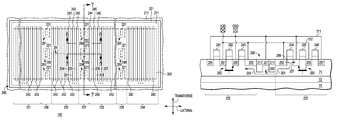
- FIG. 1 illustrates an overhead view of a portion 9 of a layout of an integrated circuit die having an ESD protection circuit comprising a MOSFET implemented using a plurality of MOSFET fingers 41 connected in parallel.
- the illustrated portion 9 includes a well-tie structure that includes a well-tie 21 and an adjacent dielectric region 11 .
- the well-tie 21 includes a ring portion 90 (the well-tie ring) having an outer periphery 20 and a plurality of dissecting portions 22 - 25 that extend across the interior of the well-tie ring 90 to divide the ESD protection circuit into a plurality of segments 31 - 35 .
- each one of the segments 31 - 35 includes a portion of the plurality of MOSFET transistors making up the ESD protection circuit.
- Each segments' set of transistors has corresponding source, drain, and channel regions within an active region 50 that is separated from the well-tie 21 by the dielectric region 11 , which can be a Shallow Trench Isolation region (STI region).
- STI region Shallow Trench Isolation region
- bipolar device that is inherently present in the layout of the MOSFET, wherein such a bipolar device is a bipolar junction transistor (BJT) that can be turned on by a mechanism commonly referenced as “snapback” to provide additional protection during an ESD event.
- BJT bipolar junction transistor
- FIG. 2 A schematic representation of such a bipolar device 60 is illustrated in FIG. 2 , which illustrates a cross-sectional layout view along the lateral cross-section indicator line 2 of FIG. 1 .
- the base of the inherent BJT 60 which is an NPN transistor, corresponds to the body of the MOSFET fingers, the collector of the BJT 60 corresponds to the drain regions of the MOSFET fingers, and the emitter of the BJT 60 corresponds to the source regions of the MOSFET fingers.
- snapback occurs due to a large voltage between the drain and the source of a MOSFET transistor of the ESD circuit that causes a change in a potential of the transistor's body region that causes the source-body junction diode of the MOSFET to turn on.
- the potential change in the body region can, for example, be due to drain-body junction leakage current during an ESD event that causes the body voltage to rise due to a voltage drop along a resistive path from the body region of the MOSFET near the MOSFETs source to a body tie.
- the large collector current can cause impact ionization current that adds to the already flowing drain-body junction leakage current, further turning on the bipolar device.
- This can ultimately result in snapback, which is a characterized by a significant increase in the current that is provided between the source and drain and which typically causes the drain-source voltage to drop or “snap back” in a corresponding I-V chart.
- Much of the current flowing from the drain to the source is flowing down in the well region that is below the MOSFET channel. This snapback event can be relied upon to provide protection by sinking current when there is an ESD event, so long as the amount of snapback current at each segments' inherent bipolar device is low enough to be non-destructive to the MOSFET features during its duration.
- the segment that first enters the snapback regime before other segments can be physically damaged if it has to sink the ESD current for a sufficiently long period of time before its ESD current load is reduced by other segments of the ESD protection circuit experiencing snapback.
- the drain-source voltage of the entire MOSFET typically drops due to the sudden reduction in the effective on-resistance of the first segment. This makes it less likely for other segments to enter the snapback regime as well because snapback is initiated by a large drain-source voltage. It is therefore desirable to increase the number of MOSFET segments that enter the snapback regime in order to maximize the failure current level of the ESD protection structure.
- a well-tie near a particular segment of an N-channel MOSFET is connected to one or more dedicated source regions of another segment. These dedicated source regions of the other segment are not connected to ground. Therefore, their voltage level gets elevated when the second segment enters bipolar conduction (snapback) due to the parasitic lateral BJT providing a current path from drain regions to the dedicated source regions. This may provide a feedback path that actively drives the well region at the well-tie in the particular segment to a higher voltage to facilitate snapback at the particular segment.
- FIG. 1 is a top view of a layout of a known overstress protection circuit
- FIG. 2 is a cross-section view of the known overstress protection circuit of FIG. 1 ;
- FIG. 3 is a circuit diagram of an overstress protection circuit according to a particular embodiment.
- FIG. 4 is a top view of a layout of the overstress protection circuitry of FIG. 3 , according to a particular embodiment
- FIG. 5 is a cross section view of the layout of FIG. 4 , according to a particular embodiment
- FIG. 6 is a cross section view of the layout of FIG. 4 , according to a particular embodiment
- FIG. 7 is a cross section view of the layout of FIG. 4 , according to a particular embodiment
- FIG. 8 is a cross section view of a well-tie region according to a particular embodiment.
- FIG. 9 is a cross section view of a well-tie region according to a particular embodiment.
- An overstress protection device for an integrated circuit die has a field-effect transistor (FET) made up of many transistor fingers connected in parallel that are laid out in a plurality of segments, each having a plurality of transistor fingers.
- the segments are separated from one another by an intervening well-tie region that includes well-ties within a source/drain region shared by two transistor fingers.
- the well-ties can be well-tie islands surrounded by the shared source/drain region, or well-ties that extend into the shared source/drain region from a well-tie ring.
- the well-ties are connected to a fixed voltage reference terminal that provides a fixed voltage, such as a ground, during normal operation.
- overstress protection device is such that current from the segment initially experiencing snapback flows more readily to an adjacent segment, not yet in snapback, along a path between the well-tie structures of a well-tie region than it does along a path that passes under the well-tie structures.
- An overstress protection devices that requires all of the inter-segment current to pass under a well-tie structure (the well-tie and its surrounding dielectric) may only experience snapback in the segment initially going into snapback and not in adjacent segments, which may cause non-uniform current conduction in the protection device and thus reduced protection from overstress conditions.
- FIG. 3 is a circuit diagram that illustrates an overstress protection circuit 100 according to an embodiment of the present disclosure.
- the overstress protection circuit comprises an N-channel MOSFET transistor, and corresponding inherent BJT, that is represented by multiple MOSFET transistors 141 - 143 connected in parallel.
- Each one of the transistors 141 - 143 can include a plurality of transistor fingers that are separated from the transistor fingers of an adjacent transistor by a well-tie region.
- each one of the transistors 141 - 143 is disposed at a particular portion of an overstress protection circuit, referred to as a segment that is represented by reference numerals 131 - 133 .
- a well-tie region 136 is between transistors 141 and 142
- a well-tie region 137 is between transistors 142 and 143 .
- Each of well-tie regions 136 - 137 includes a corresponding well-tie 121 (WT 121 ) that is connected to terminal GND, as will be further discussed herein.
- Segment 131 also referred to as transistor segment 131 , includes MOSFET 141 and a corresponding inherent BJT 161 .
- the collector, emitter, and base of BJT 161 correspond to the drain, source, and body of transistor 141 , respectively.
- Transistor segment 132 also referred to as transistor segment 132 , includes MOSFET 142 and a corresponding inherent BJT 162 .
- the collector, emitter, and base of BJT 162 correspond to the drain, source, and body of transistor 142 , respectively.
- Transistor segment 133 also referred to as transistor segment 133 , includes MOSFET 143 and a corresponding inherent BJT 163 .
- the collector, emitter, and base of BJT 163 correspond to the drain, source, and body of transistor 143 , respectively.
- each segments' MOSFET/BJT pair is connected to a terminal labeled VDD that is protected by the overstress protection circuit 100 .
- Terminal VDD can be a conductive node at which a fixed voltage reference is provided, such as VDD.
- the source/emitter of each segments' MOSFET/BJT pair is connected to a terminal labeled GND at which a fixed voltage, such as ground, is provided during operation.
- the fixed voltages are provided to the terminals GND and VDD during normal operation, and can be generated by a voltage regulator disposed at the same integrated circuit die as the overstress protection circuit, or can be provided from a voltage source external to the integrated circuit die.
- each MOSFET 141 - 143 can be connected (not shown) to a terminal that provides a fixed voltage, such as terminal GND, or to an output terminal of a driver circuit that operates to turn on the MOSFETs 141 - 143 during an overstress event. In another embodiment, there can be an intervening resistor between the gate and source of each transistor.
- the body-to-well-tie resistance of each segment is illustrated as resistor Rbw, and is the resistance between the body of each segments' MOSFET and the well-ties 121 at which a fixed voltage is provided.
- the well-ties 121 are connected to terminal GND.
- the body-to-body resistance from the body of one segment's MOSFET to the body of an adjacent segment's MOSFET is illustrated as resistor Rbb.
- the transistors of FIG. 3 remain non-conductive.
- avalanche current from a drain-body junction of one of the transistor segments can introduce a current to the well region that causes a voltage drop along the body-to-well-tie resistive path (Rbw).
- this voltage drop can trigger a high-current snapback resulting in the BJT turning on.
- the resistance Rbb is lower than in other protection devices having continuous well-ties connected to fixed voltage terminals that extend across the well-tie ring, without paths between transistor segments.
- FIG. 4 illustrates an embodiment of a layout of the overstress protection device 100 of FIG. 3 having well-ties 221 and a plurality of MOSFET transistor fingers 240 arranged in a plurality of segments 231 - 234 . Segments 231 - 233 correspond to segments 131 - 133 of FIG. 3 .
- Well-ties 221 include a well-tie ring 290 and a plurality of separate well-tie islands at well-tie regions 236 - 238 that are disposed within the well-tie ring.
- the term “well-tie island” as used herein is intended to refer to a well-tie between transistor segments with the well-tie physically separated from the well-tie ring. For purposes of discussion, it is presumed that the well-tie of a well-tie island is a region of p-doped silicon, and the dielectric surrounding the well-tie island is presumed to be an STI region 211 .
- Each one of the plurality of MOSFET transistor fingers 240 includes a transistor gate and adjacent source/drain regions formed within corresponding portions of active regions 250 , wherein, with the exception of the well-tie islands 221 , the region of FIG. 4 between active regions 250 and well-tie ring 290 is a portion of the STI region 211 .
- each one of the plurality of MOSFET transistor fingers 240 can be referred to as a MOSFET transistor finger, a MOSFET finger, a transistor finger, a finger, and variations thereof, to indicate it is one of a plurality of transistor fingers connected in parallel to make up a larger transistor.
- Transistor fingers 241 - 246 are specifically identified members of the plurality of MOSFET fingers 240 .
- MOSFET finger 241 shares a source/drain region 251 with MOSFET finger 242 .
- MOSFET finger 242 shares a source/drain region 255 with MOSFET finger 243 .
- MOSFET finger 243 shares a source/drain region 252 with MOSFET finger 244 ,
- MOSFET 244 shares a source/drain region 256 with MOSFET finger 245 , and
- MOSFET finger 245 shares a source/drain region 253 with MOSFET finger 246 .
- source/drain is intended to generically refer to both source and drain regions. As will be illustrated at FIG. 5 , according to an embodiment source/drain regions 254 - 257 are presumed to be source regions connected to terminal GND, and source/drain regions 251 - 253 are presumed to be drain regions connected to terminal VDD.
- the plurality of MOSFET fingers 240 are partitioned into sets that are disposed at segments 231 - 234 .
- Each one of the segments 231 - 234 is distinguished from an adjacent segment by a well-tie region 236 - 238 that includes one or more well-ties.
- segment 232 is distinguished from segment 231 by well-tie region 236 which includes well-tie structures 291 - 293 , each of which includes a corresponding well-tie island 221 .
- Segment 232 is distinguished from segment 233 by well-tie region 237 which includes well-tie structures 294 - 296 , each of which includes a corresponding well-tie island 221 .
- Segment 233 is distinguished from segment 234 by well-tie region 238 , which includes well-tie structures 297 - 299 , each of which includes a corresponding well-tie island 221 .
- the MOSFET formed by the MOSFET fingers within a segment is referred to herein as a MOSFET transistor segment, or a MOSFET segment.
- each of the MOSFET transistor segments operates simultaneously as a common MOSFET transistor of a high-voltage protection circuit as they are connected in parallel.
- the number of well-tie islands at a well-tie region can vary from that illustrated.
- each well-tie region between segments can include more or fewer well-tie islands than that illustrated.
- a well-tie island can be disposed at a center location of a well-tie region in a transverse direction.
- transverse direction as used herein is intended to mean the direction defined by the edge of a gate of a MOSFET transistor along its width, wherein it will be understood that width of the MOSFET transistor fingers illustrated at FIG. 4 is significantly longer than length of the fingers.
- the center location of a well-tie region in a transverse direction is located halfway between the upper-most location of the source/drain region 252 and a lower-most portion of the source/drain region 252 , and is indicated by the line 291 .
- the well-tie islands 292 , 295 , and 298 are each disposed at the center location of their respective well-tie regions 236 - 238 .
- the total number of transistor segments in a high-voltage protection device can be an odd or even number.
- the device illustrated FIG. 5 includes an odd number of segments, and that segment 233 is the center segment of the odd number of segments.
- segment 233 could represent a non-center segment of a device having either an odd or even number of segments.
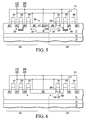
- FIG. 4 illustrates cross-sectional indicators having reference numbers 5 - 7 that correspond to FIGS. 5-7 , respectively.
- FIG. 5 illustrates a cross-sectional layout view along the lateral cross-section indicator line 5 of FIG. 4 , and a circuit representation of various other features.
- lateral is intended to refer to the direction orthogonal to the transverse direction, described above, that is also the direction of current flow through channel regions of the MOSFETs 240 when turned-on during normal operation (e.g., not during a high-voltage event).
- the plurality of transistors 240 each include a gate stack overlying a channel region, and source/drain regions abutting the channel region. (Note that only transistors 241 - 246 of the plurality of transistors 240 are illustrated.) Therefore, each of the source/drain regions 251 - 257 of transistors 241 - 246 , specifically illustrated at FIG. 5 , is shared by abutting transistors. A conductive control gate is also illustrated as overlying a gate dielectric for each of transistors 241 - 246 . For purposes of discussion, the source/drain regions 251 - 257 are presumed to be N-doped semiconductor regions residing in a P-type well 71 that correspond to channel and body regions of the MOSFETs 241 - 246 .
- Well-tie structure 295 is an island structure disposed between a portion of drain 252 that abuts the gate of transistor 244 and a portion of the drain 252 that abuts the gate of transistor 243 .
- well-tie structures, and their corresponding well-ties are disposed in a lateral direction between the gate of a leftmost transistor finger of one segment, such as segment 233 , and the gate of a rightmost transistor finger of another segment, such as segment 232 .
- Well-tie island 221 of well-tie island structure 295 is connected to terminal GND via the interconnect 311 to complete a well-tie connection to the well region 71 .
- Each of the source/drain regions 251 - 257 is connected to one of either the VDD terminal via an interconnect 312 , or to the GND terminal via an interconnect 311 .
- source/drain regions 251 - 253 are drain regions connected to the VDD terminal, and, therefore are also collector portions of the protective device's BJTs, as illustrated by the circuit representation of BJTs 262 and 263 .
- BJTs 262 and 263 can be presumed to represent each FET of their respective segments.
- Source/drain regions 254 - 257 are source regions connected to the GND terminal via interconnect 311 , and therefore are also emitter portions of the protective device's BJTs, as illustrated by BJTs 262 and 263 .
- the P-type well 71 which constitutes the body of the transistors 241 - 246 , overlies a layer 72 that can be an oxide layer, N-doped layer, or other appropriate layer. In some embodiments layer 72 may not be present. Layer 72 overlies a substrate 73 , which can be a P-doped silicon substrate, or other appropriate layer that provides structural support for layers 71 and 72 .
- the well-tie 221 is an interface region between the interconnect 311 of the device and the P-doped well region 71 .
- the well-tie 221 is a P-doped silicon region typically having a higher doping concentration than that of the well 71 , which is of the same conductivity type, i.e., is P-doped. It will be appreciated, that the well-tie can also include additional features, such as a silicide region (not illustrated).
- Line 206 of FIG. 5 represents current from the drain region 252 that is part of MOSFET finger 244 during a snapback event originating from segment 233 .
- Line 207 of FIG. 5 represents the snapback current that flows from drain region 252 to source 256 during snapback.
- Line 201 of FIG. 5 represents a current path ( 201 ) from segment 233 to segment 232 .
- the current along path 201 can be generated during snapback of the transistor of segment 233 , and flows from drain region 252 to well region 71 , and then under the well-tie island 295 , via well region 71 , before reaching segment 232 .
- a portion 202 of the current 201 is illustrated as flowing towards the well-tie 221 because the well-tie 221 is at a low-voltage bias potential, leaving only a portion 203 of the current 201 to flow to the body regions of the adjacent segments to elevate the body potentials of the MOSFET transistor fingers in the adjacent segment during snapback of segment 233 .
- FIG. 6 illustrates a cross-sectional layout view along the lateral cross-section indicator line 6 of FIG. 4 .
- the view of FIG. 6 is similar to the view of FIG. 5 , except that the view of FIG. 6 does not intersect a well-tie. Instead, at the view of FIG. 6 the shared source/drain region 252 is continuous between the gate of transistor 243 and the gate of transistor 244 .
- the well-tie island 221 of well-tie structure 295 is surrounded by the shared drain region 252 , and that well-tie islands 221 of well-tie structures 294 and 296 ( FIG.
- Lines 206 and 207 of FIG. 6 represent the current from the drain region 252 and the snapback current that flows to source 256 , respectively, as described above.
- Line 208 represents a current path from segment 233 to segment 232 . The current along path 208 can be generated during snapback of the transistor of segment 233 , and flows from the drain region 252 to the well region 71 of segment 232 .
- path 208 can be lower than the resistance along paths 201 and 203 of FIG. 5 due at least partially to path 208 being a more direct path from segment 233 to segment 232 by virtue of being closer to the silicon surface, and by virtue of being within a highly doped region which can be less resistive than a path deeper in the well region.
- Path 208 may also have a deeper region of the well available for current flow, as measured between drain region 252 and layer 72 , which typically provides a less resistive path than the shallower region between STI regions 211 and layer 72 for paths 201 and 203 . Furthermore, a substantial portion of the current along path 201 in FIG.
- FIG. 7 illustrates a cross-sectional layout view along the transverse cross-section indicator line 7 of FIG. 4 , and a circuit representation of various other features. Specifically illustrated are cross-sectional portions of the well-tie islands of structures 294 - 296 , the well-tie ring 290 , shared drain region 252 , and circuit representations of interconnects 311 , 312 , and terminals VDD and GND. Note that by virtue of the well-tie island structure 295 being surrounded by the shared source/drain region 252 , it is disposed between two portions of the shared source/drain region 252 in the transverse direction ( FIG. 7 ) as well as in the lateral direction ( FIG. 5 ).
- Well-tie island structures 294 and 296 are not disposed between portions of the shared source/drain region in the transverse direction ( FIG. 7 ), but are disposed between portions of the shared source/drain region in the lateral direction ( FIG. 5 ).
- the well-tie island structures 294 and 296 can be positioned so that they too are surrounded by drain region 252 .
- the transverse dimension 314 of the drain region between well-tie island structures which is the shortest distance between the structures, is two or more times greater than the transverse dimension 313 of well-tie island structures.
- the ratio of the transverse dimension of the drain region between well-tie island structures to the transverse dimension of the well-tie island structures can be 1:1, greater than 1:1, greater than 2:1, or less than 1:1. In other embodiments, the ratio can be any number suitable for improving the propagation of snapback current between adjacent segments while maintaining enough effective well tie area between segments for maintaining latch-up robustness of the protection structure.
- the disclosed overstress circuit provides a lower-resistance and unobstructed path between segments than other configurations.
- This path allows current to more readily flow from a segment experiencing snapback to an adjacent segment not yet in snapback through a well layer, because the current does not need to pass under a well-tie and its adjacent, relatively deep STI regions.
- a greater amount of current is more readily introduced to segments adjacent to the initial snapback segment due to the difference in potential between the well of the segment initially experiencing snapback and the well of adjacent segments.
- FIG. 8 illustrates an overhead view of a portion of an overstress protection circuit that includes an embodiment of a well-tie region 437 between segments 432 and 433 including well-tie island structures 495 , 496 and well-tie ring extension structures 494 , 497 .
- well-tie ring extension as used herein is intended to refer to a well-tie portion that is contiguous with a well-tie ring, and extends inward from the well-tie ring.
- well-tie ring extension structures 494 , 497 include well-ties that extend inward from the well-tie ring 290 in the transverse direction.
- the well-tie island structures 495 , 496 are between shared source/drain region 252 in a lateral direction and in a transverse direction by virtue of being surrounded by the shared source/drain region 252 .
- the well-tie ring extensions 494 , 497 are between the shared source/drain region 252 in a lateral direction, but not in a transverse direction.
- FIG. 9 illustrates an overhead view of a portion of an overstress protection circuit that includes an embodiment of a well-tie region 537 between segments 532 and 533 including well-tie ring extension structures 594 , 595 , but not well-tie islands.
- the well-tie extension structures 594 , 595 extend inward from the well-tie ring 290 in the transverse direction.
- the well-tie ring extension structures 594 , 595 are between the shared source/drain region 252 in a lateral direction, but not in a transverse direction.
- the well-tie extension structures 594 , 595 do not connect within the well-tie region 537 , a single low-resistance “bridge” is formed between the well-tie extension structures 594 , 595 through which well current can more readily flow, as opposed to the well resistance of a current path underlying the well-tie extension structures 495 and 496 .
- the shared source/drain region 252 of FIG. 9 resides at the center location of the well-tie region 537 in a transverse direction. In other embodiments, the shared source/drain region 252 does not need to reside at the center location.
- An integrated circuit device can include a Field Effect Transistor (FET) including a first transistor finger and a second transistor finger, wherein the first transistor finger and the second transistor finger share a first source/drain region of a first conductivity type residing in a well region having a second conductivity type, wherein the first conductivity type is opposite the second conductivity type.
- FET Field Effect Transistor
- the integrated circuit device can also include a first well-tie between a first portion of the first source/drain region and a second portion of the first source/drain region, the first well-tie coupled to a voltage reference terminal that provides a fixed bias voltage for the well region during normal operation of the integrated circuit.
- the first well-tie is between the first and second portions of the first source/drain region in a lateral direction. In another embodiment of the first aspect, the first well-tie is between the first and second portions of the first source/drain region in a transverse direction. In a further embodiment of the first aspect, the first well-tie is surrounded by the first source/drain region.
- the device includes a second well-tie between the second portion of the first source/drain region and a third portion of the first source/drain region, wherein the first well-tie and a surrounding dielectric region are surrounded by the first source/drain region.
- the second portion of the first source/drain region is at a center location of the first source/drain region in a transverse direction.
- the first well-tie is at a center location of the first source/drain region in a transverse direction.
- a gate of the first transistor finger and a gate of the second transistor finger are coupled together.
- a ratio of a first dimension to a second dimension is at least 1:1, wherein the first dimension is a shortest distance in a transverse direction between a dielectric of the first well-tie and a dielectric of the second well-tie, and the second dimension is a length of the first well-tie and its surrounding dielectric in the transverse direction.
- the ratio is at least 2:1.
- a gate of the first transistor finger and a gate of the second transistor are coupled together.
- the first source/drain region is a source region that is coupled to the voltage reference terminal.
- a method can include providing a first current from a source/drain region of a first Field Effect Transistor (a first FET) to a first well region of the first FET in response to an overstress event, receiving a snapback portion of the first current at a second source/drain region of the first FET, and receiving, via a current path, a biasing portion of the first current at a second well region closer to a second FET than to the first FET, wherein the current path includes a third well region abutting a shared source/drain region that is shared by the first FET and the second FET, and that extends continuously from a gate of the first FET to a gate of the second FET.
- a first FET Field Effect Transistor
- a device can include an integrated circuit electrical protection device including a Field Effect Transistor (FET) including a plurality of transistor fingers, including a first transistor finger and a second transistor finger, each of the plurality of transistor fingers including a gate portion, a source region, and a drain region shared with another one of the plurality of transistor fingers, wherein the first transistor finger shares a first drain region with the second transistor finger, and the source region is coupled to a fixed voltage reference terminal.
- the method can further include a first well-tie between a first portion of the first drain region and a second portion of the first drain region, the first well-tie coupled to the fixed voltage reference terminal that is to provide a fixed voltage during normal operation.
- the first well-tie is surrounded by the first drain region.
- the device includes a second well-tie is between the second portion of the first drain region and a third portion of the first drain region.
- the second portion of the first drain region is at a center location of the first drain region relative a width of the first drain region.
- the first well-tie is at a center location of the first drain region in a transverse direction.
- ratio of a dimension between the first and second well-ties to a width of the first well-tie is at least 1:1, wherein the dimension and the width are relative to a width of the first drain region.
- the ratio is at least 2:1, wherein the dimension and the width are relative to a width of the first drain region.
- the plurality of transistor fingers further include a third transistor finger and a fourth transistor finger, the third transistor finger shares a second drain region with the fourth transistor finger, and the FET transistor further includes a second well-tie between a first portion of the second drain region and a second portion of the second drain region, the second well-tie coupled to the fixed voltage reference terminal, and the second and third transistor fingers are members of a set of the plurality of transistor fingers, wherein no well-ties reside between gates of the members of the set.
- the first well-tie is one of a first plurality of well-ties within the first drain region
- the second well-tie is one of a second plurality of well-ties within the second drain region.
- the change in body potential is described as an increase but may, in the proper situation, be a decrease.
- the conductivity types of the various doped regions may be able to be reversed to obtain analogous operation but using P type transistors and PNP inherent bipolar transistors.
- the illustrated embodiments address a protection circuit that monitors a fixed terminal, VDD, for an overstress event, a similar circuit can be used to protect terminals that transmit data signals, such as analog or digital data signals.
- field effect transistors FETs
- MOSFETs metal oxide semiconductor field effect transistors
Landscapes
- Semiconductor Integrated Circuits (AREA)
- Metal-Oxide And Bipolar Metal-Oxide Semiconductor Integrated Circuits (AREA)
Abstract
Description
Claims (20)
Applications Claiming Priority (3)
| Application Number | Priority Date | Filing Date | Title |
|---|---|---|---|
| CN201410117590 | 2014-03-27 | ||
| CN201410117590.6A CN104952866B (en) | 2014-03-27 | 2014-03-27 | Integrated circuit electric protective device |
| CN201410117590.6 | 2014-03-27 |
Publications (2)
| Publication Number | Publication Date |
|---|---|
| US20150279836A1 US20150279836A1 (en) | 2015-10-01 |
| US9202808B2 true US9202808B2 (en) | 2015-12-01 |
Family
ID=54167413
Family Applications (1)
| Application Number | Title | Priority Date | Filing Date |
|---|---|---|---|
| US14/231,849 Active 2034-04-02 US9202808B2 (en) | 2014-03-27 | 2014-04-01 | Integrated circuit electrical protection device |
Country Status (2)
| Country | Link |
|---|---|
| US (1) | US9202808B2 (en) |
| CN (1) | CN104952866B (en) |
Cited By (1)
| Publication number | Priority date | Publication date | Assignee | Title |
|---|---|---|---|---|
| US20230054540A1 (en) * | 2021-08-17 | 2023-02-23 | International Business Machines Corporation | Optimized Contact Resistance for Stacked FET Devices |
Families Citing this family (1)
| Publication number | Priority date | Publication date | Assignee | Title |
|---|---|---|---|---|
| DE102016119813B4 (en) * | 2016-10-18 | 2024-03-28 | Infineon Technologies Ag | Electrostatic discharge protection structure and method of manufacturing an electrostatic discharge protection structure |
Citations (5)
| Publication number | Priority date | Publication date | Assignee | Title |
|---|---|---|---|---|
| US7002220B1 (en) * | 2003-01-29 | 2006-02-21 | Marvell International Ltd. | ESD protection circuit |
| US7005708B2 (en) | 2001-06-14 | 2006-02-28 | Sarnoff Corporation | Minimum-dimension, fully-silicided MOS driver and ESD protection design for optimized inter-finger coupling |
| US7098510B2 (en) * | 2003-07-28 | 2006-08-29 | Nec Electronics Corporation | Multifinger-type electrostatic discharge protection element |
| US7170726B2 (en) | 2003-01-16 | 2007-01-30 | Silicon Integrated Systems Corp. | Uniform turn-on design on multiple-finger MOSFET for ESD protection application |
| US9076656B2 (en) * | 2013-05-02 | 2015-07-07 | Freescale Semiconductor, Inc. | Electrostatic discharge (ESD) clamp circuit with high effective holding voltage |
Family Cites Families (6)
| Publication number | Priority date | Publication date | Assignee | Title |
|---|---|---|---|---|
| US8207577B2 (en) * | 2009-09-29 | 2012-06-26 | Power Integrations, Inc. | High-voltage transistor structure with reduced gate capacitance |
| JP5529607B2 (en) * | 2010-03-29 | 2014-06-25 | セイコーインスツル株式会社 | Semiconductor device |
| US8476684B2 (en) * | 2010-09-29 | 2013-07-02 | Analog Devices, Inc. | Field effect transistors having improved breakdown voltages and methods of forming the same |
| ITMI20112278A1 (en) * | 2011-12-15 | 2013-06-16 | St Microelectronics Srl | BIPOLAR POWER STRUCTURE, IN PARTICULAR FOR HIGH VOLTAGE APPLICATIONS |
| US8575694B2 (en) * | 2012-02-13 | 2013-11-05 | Taiwan Semiconductor Manufacturing Company, Ltd. | Insulated gate bipolar transistor structure having low substrate leakage |
| CN103151351A (en) * | 2013-03-29 | 2013-06-12 | 西安电子科技大学 | Self substrate trigger ESD (Electro-Static Discharge) protecting device using dynamic substrate resistance technology, and application |
-
2014
- 2014-03-27 CN CN201410117590.6A patent/CN104952866B/en active Active
- 2014-04-01 US US14/231,849 patent/US9202808B2/en active Active
Patent Citations (5)
| Publication number | Priority date | Publication date | Assignee | Title |
|---|---|---|---|---|
| US7005708B2 (en) | 2001-06-14 | 2006-02-28 | Sarnoff Corporation | Minimum-dimension, fully-silicided MOS driver and ESD protection design for optimized inter-finger coupling |
| US7170726B2 (en) | 2003-01-16 | 2007-01-30 | Silicon Integrated Systems Corp. | Uniform turn-on design on multiple-finger MOSFET for ESD protection application |
| US7002220B1 (en) * | 2003-01-29 | 2006-02-21 | Marvell International Ltd. | ESD protection circuit |
| US7098510B2 (en) * | 2003-07-28 | 2006-08-29 | Nec Electronics Corporation | Multifinger-type electrostatic discharge protection element |
| US9076656B2 (en) * | 2013-05-02 | 2015-07-07 | Freescale Semiconductor, Inc. | Electrostatic discharge (ESD) clamp circuit with high effective holding voltage |
Non-Patent Citations (2)
| Title |
|---|
| Huh, Y. et al., "The Effects of Substrate Coupling on Triggering Uniformity and ESD Failure Threshold of Fully Silicided NMOS Transistors," IEEE 2002 Symposium on VLSI Technology Digest of Technical Papers; Jun. 11-13, 2002; ISBN: 0-7803-7312-X; pp. 220-221. |
| Ker, M. et al.; "Self-Substrate-Triggered Technique to Enhance Turn-on Uniformity of Multi-Finger ESD Protection Devices"; 2005 VLSI-TSA International Symposium on VLSI Technology; Apr. 25-27, 2005; pp. 17-18. |
Cited By (2)
| Publication number | Priority date | Publication date | Assignee | Title |
|---|---|---|---|---|
| US20230054540A1 (en) * | 2021-08-17 | 2023-02-23 | International Business Machines Corporation | Optimized Contact Resistance for Stacked FET Devices |
| US11948944B2 (en) * | 2021-08-17 | 2024-04-02 | International Business Machines Corporation | Optimized contact resistance for stacked FET devices |
Also Published As
| Publication number | Publication date |
|---|---|
| US20150279836A1 (en) | 2015-10-01 |
| CN104952866B (en) | 2019-07-12 |
| CN104952866A (en) | 2015-09-30 |
Similar Documents
| Publication | Publication Date | Title |
|---|---|---|
| US9559170B2 (en) | Electrostatic discharge protection devices | |
| US9704850B2 (en) | Electrostatic discharge protection device comprising a silicon controlled rectifier | |
| CN104241272B (en) | Electrostatic discharge transistor and its electrostatic discharge protection circuit | |
| US10141300B1 (en) | Low capacitance transient voltage suppressor | |
| US7098510B2 (en) | Multifinger-type electrostatic discharge protection element | |
| US11133299B2 (en) | Gate-lifted NMOS ESD protection device | |
| US9472511B2 (en) | ESD clamp with a layout-alterable trigger voltage and a holding voltage above the supply voltage | |
| US9153569B1 (en) | Segmented NPN vertical bipolar transistor | |
| US10177136B2 (en) | Electrostatic discharge protection device for high voltage | |
| US9202760B2 (en) | Semiconductor devices and structures | |
| US20120098046A1 (en) | Electrostatic discharge protection device | |
| JP5968548B2 (en) | Semiconductor device | |
| US9502399B1 (en) | Diode string circuit configurations with improved parasitic silicon-controlled rectifier (SCR) conduction during electrostatic discharge (ESD) events | |
| US10147716B2 (en) | Electrostatic discharge protection apparatus and applications thereof | |
| US20080169509A1 (en) | Semiconductor device | |
| US9087849B2 (en) | Electrostatic discharge protection devices | |
| US9202808B2 (en) | Integrated circuit electrical protection device | |
| KR101130766B1 (en) | Electro-Static Discharge Protection Device | |
| US9153570B2 (en) | ESD tolerant I/O pad circuit including a surrounding well | |
| CN100505241C (en) | Semiconductor protection device | |
| KR20220004487A (en) | Electro-static discharge protection device having a low trigger voltage | |
| JP2005101485A (en) | Electrostatic discharge protection element |
Legal Events
| Date | Code | Title | Description |
|---|---|---|---|
| AS | Assignment |
Owner name: FREESCALE SEMICONDUCTOR, INC., TEXAS Free format text: ASSIGNMENT OF ASSIGNORS INTEREST;ASSIGNORS:STOCKINGER, MICHAEL A.;ZHANG, WENZHONG;ZHANG, XU;SIGNING DATES FROM 20140318 TO 20140325;REEL/FRAME:032570/0388 |
|
| AS | Assignment |
Owner name: CITIBANK, N.A., AS NOTES COLLATERAL AGENT, NEW YORK Free format text: SUPPLEMENT TO IP SECURITY AGREEMENT;ASSIGNOR:FREESCALE SEMICONDUCTOR, INC.;REEL/FRAME:033460/0337 Effective date: 20140729 Owner name: CITIBANK, N.A., AS NOTES COLLATERAL AGENT, NEW YORK Free format text: SUPPLEMENT TO IP SECURITY AGREEMENT;ASSIGNOR:FREESCALE SEMICONDUCTOR, INC.;REEL/FRAME:033462/0293 Effective date: 20140729 Owner name: CITIBANK, N.A., AS NOTES COLLATERAL AGENT, NEW YORK Free format text: SUPPLEMENT TO IP SECURITY AGREEMENT;ASSIGNOR:FREESCALE SEMICONDUCTOR, INC.;REEL/FRAME:033462/0267 Effective date: 20140729 Owner name: CITIBANK, N.A., AS NOTES COLLATERAL AGENT, NEW YOR Free format text: SUPPLEMENT TO IP SECURITY AGREEMENT;ASSIGNOR:FREESCALE SEMICONDUCTOR, INC.;REEL/FRAME:033460/0337 Effective date: 20140729 Owner name: CITIBANK, N.A., AS NOTES COLLATERAL AGENT, NEW YOR Free format text: SUPPLEMENT TO IP SECURITY AGREEMENT;ASSIGNOR:FREESCALE SEMICONDUCTOR, INC.;REEL/FRAME:033462/0293 Effective date: 20140729 Owner name: CITIBANK, N.A., AS NOTES COLLATERAL AGENT, NEW YOR Free format text: SUPPLEMENT TO IP SECURITY AGREEMENT;ASSIGNOR:FREESCALE SEMICONDUCTOR, INC.;REEL/FRAME:033462/0267 Effective date: 20140729 |
|
| STCF | Information on status: patent grant |
Free format text: PATENTED CASE |
|
| AS | Assignment |
Owner name: FREESCALE SEMICONDUCTOR, INC., TEXAS Free format text: PATENT RELEASE;ASSIGNOR:CITIBANK, N.A., AS COLLATERAL AGENT;REEL/FRAME:037357/0903 Effective date: 20151207 |
|
| AS | Assignment |
Owner name: MORGAN STANLEY SENIOR FUNDING, INC., MARYLAND Free format text: ASSIGNMENT AND ASSUMPTION OF SECURITY INTEREST IN PATENTS;ASSIGNOR:CITIBANK, N.A.;REEL/FRAME:037444/0082 Effective date: 20151207 Owner name: MORGAN STANLEY SENIOR FUNDING, INC., MARYLAND Free format text: ASSIGNMENT AND ASSUMPTION OF SECURITY INTEREST IN PATENTS;ASSIGNOR:CITIBANK, N.A.;REEL/FRAME:037444/0109 Effective date: 20151207 |
|
| AS | Assignment |
Owner name: MORGAN STANLEY SENIOR FUNDING, INC., MARYLAND Free format text: SECURITY AGREEMENT SUPPLEMENT;ASSIGNOR:NXP B.V.;REEL/FRAME:038017/0058 Effective date: 20160218 |
|
| AS | Assignment |
Owner name: MORGAN STANLEY SENIOR FUNDING, INC., MARYLAND Free format text: SUPPLEMENT TO THE SECURITY AGREEMENT;ASSIGNOR:FREESCALE SEMICONDUCTOR, INC.;REEL/FRAME:039138/0001 Effective date: 20160525 |
|
| AS | Assignment |
Owner name: MORGAN STANLEY SENIOR FUNDING, INC., MARYLAND Free format text: CORRECTIVE ASSIGNMENT TO CORRECT THE REMOVE APPLICATION 12092129 PREVIOUSLY RECORDED ON REEL 038017 FRAME 0058. ASSIGNOR(S) HEREBY CONFIRMS THE SECURITY AGREEMENT SUPPLEMENT;ASSIGNOR:NXP B.V.;REEL/FRAME:039361/0212 Effective date: 20160218 |
|
| AS | Assignment |
Owner name: MORGAN STANLEY SENIOR FUNDING, INC., MARYLAND Free format text: CORRECTIVE ASSIGNMENT TO CORRECT THE REMOVE APPLICATION 14/258,829 AND REPLACE ITWITH 14/258,629 PREVIOUSLY RECORDED ON REEL 037444 FRAME 0082. ASSIGNOR(S) HEREBY CONFIRMS THE ASSIGNMENT AND ASSUMPTION OFSECURITY INTEREST IN PATENTS;ASSIGNOR:CITIBANK, N.A.;REEL/FRAME:039639/0332 Effective date: 20151207 Owner name: MORGAN STANLEY SENIOR FUNDING, INC., MARYLAND Free format text: CORRECTIVE ASSIGNMENT TO CORRECT THE REMOVE APPLICATION14/258,829 AND REPLACE IT WITH 14/258,629 PREVIOUSLY RECORDED ON REEL 037444 FRAME 0109. ASSIGNOR(S) HEREBY CONFIRMS THE ASSIGNMENT AND ASSUMPTION OF SECURITY INTEREST IN PATENTS;ASSIGNOR:CITIBANK, N.A.;REEL/FRAME:039639/0208 Effective date: 20151207 Owner name: MORGAN STANLEY SENIOR FUNDING, INC., MARYLAND Free format text: CORRECTIVE ASSIGNMENT OF INCORRECT APPLICATION 14/258,829 PREVIOUSLY RECORDED ON REEL 037444 FRAME 0109. ASSIGNOR(S) HEREBY CONFIRMS THE ASSIGNMENT AND ASSUMPTION OF SECURITY INTEREST IN PATENTS;ASSIGNOR:CITIBANK, N.A.;REEL/FRAME:039639/0208 Effective date: 20151207 |
|
| AS | Assignment |
Owner name: NXP, B.V., F/K/A FREESCALE SEMICONDUCTOR, INC., NETHERLANDS Free format text: RELEASE BY SECURED PARTY;ASSIGNOR:MORGAN STANLEY SENIOR FUNDING, INC.;REEL/FRAME:040925/0001 Effective date: 20160912 Owner name: NXP, B.V., F/K/A FREESCALE SEMICONDUCTOR, INC., NE Free format text: RELEASE BY SECURED PARTY;ASSIGNOR:MORGAN STANLEY SENIOR FUNDING, INC.;REEL/FRAME:040925/0001 Effective date: 20160912 |
|
| AS | Assignment |
Owner name: NXP B.V., NETHERLANDS Free format text: RELEASE BY SECURED PARTY;ASSIGNOR:MORGAN STANLEY SENIOR FUNDING, INC.;REEL/FRAME:040928/0001 Effective date: 20160622 |
|
| AS | Assignment |
Owner name: NXP USA, INC., TEXAS Free format text: CHANGE OF NAME;ASSIGNOR:FREESCALE SEMICONDUCTOR, INC.;REEL/FRAME:040632/0001 Effective date: 20161107 |
|
| AS | Assignment |
Owner name: MORGAN STANLEY SENIOR FUNDING, INC., MARYLAND Free format text: CORRECTIVE ASSIGNMENT TO CORRECT THE REMOVE APPLICATION 12681366 PREVIOUSLY RECORDED ON REEL 039361 FRAME 0212. ASSIGNOR(S) HEREBY CONFIRMS THE SECURITY AGREEMENT SUPPLEMENT;ASSIGNOR:NXP B.V.;REEL/FRAME:042762/0145 Effective date: 20160218 Owner name: MORGAN STANLEY SENIOR FUNDING, INC., MARYLAND Free format text: CORRECTIVE ASSIGNMENT TO CORRECT THE REMOVE APPLICATION 12681366 PREVIOUSLY RECORDED ON REEL 038017 FRAME 0058. ASSIGNOR(S) HEREBY CONFIRMS THE SECURITY AGREEMENT SUPPLEMENT;ASSIGNOR:NXP B.V.;REEL/FRAME:042985/0001 Effective date: 20160218 |
|
| AS | Assignment |
Owner name: NXP USA, INC., TEXAS Free format text: CORRECTIVE ASSIGNMENT TO CORRECT THE NATURE OF CONVEYANCE PREVIOUSLY RECORDED AT REEL: 040632 FRAME: 0001. ASSIGNOR(S) HEREBY CONFIRMS THE MERGER AND CHANGE OF NAME;ASSIGNOR:FREESCALE SEMICONDUCTOR INC.;REEL/FRAME:044209/0047 Effective date: 20161107 |
|
| MAFP | Maintenance fee payment |
Free format text: PAYMENT OF MAINTENANCE FEE, 4TH YEAR, LARGE ENTITY (ORIGINAL EVENT CODE: M1551); ENTITY STATUS OF PATENT OWNER: LARGE ENTITY Year of fee payment: 4 |
|
| AS | Assignment |
Owner name: NXP B.V., NETHERLANDS Free format text: RELEASE BY SECURED PARTY;ASSIGNOR:MORGAN STANLEY SENIOR FUNDING, INC.;REEL/FRAME:050744/0097 Effective date: 20190903 Owner name: NXP B.V., NETHERLANDS Free format text: RELEASE BY SECURED PARTY;ASSIGNOR:MORGAN STANLEY SENIOR FUNDING, INC.;REEL/FRAME:050745/0001 Effective date: 20190903 |
|
| AS | Assignment |
Owner name: MORGAN STANLEY SENIOR FUNDING, INC., MARYLAND Free format text: CORRECTIVE ASSIGNMENT TO CORRECT THE REMOVE APPLICATION 12298143 PREVIOUSLY RECORDED ON REEL 042762 FRAME 0145. ASSIGNOR(S) HEREBY CONFIRMS THE SECURITY AGREEMENT SUPPLEMENT;ASSIGNOR:NXP B.V.;REEL/FRAME:051145/0184 Effective date: 20160218 Owner name: MORGAN STANLEY SENIOR FUNDING, INC., MARYLAND Free format text: CORRECTIVE ASSIGNMENT TO CORRECT THE REMOVE APPLICATION 12298143 PREVIOUSLY RECORDED ON REEL 039361 FRAME 0212. ASSIGNOR(S) HEREBY CONFIRMS THE SECURITY AGREEMENT SUPPLEMENT;ASSIGNOR:NXP B.V.;REEL/FRAME:051029/0387 Effective date: 20160218 Owner name: MORGAN STANLEY SENIOR FUNDING, INC., MARYLAND Free format text: CORRECTIVE ASSIGNMENT TO CORRECT THE REMOVE APPLICATION 12298143 PREVIOUSLY RECORDED ON REEL 042985 FRAME 0001. ASSIGNOR(S) HEREBY CONFIRMS THE SECURITY AGREEMENT SUPPLEMENT;ASSIGNOR:NXP B.V.;REEL/FRAME:051029/0001 Effective date: 20160218 Owner name: MORGAN STANLEY SENIOR FUNDING, INC., MARYLAND Free format text: CORRECTIVE ASSIGNMENT TO CORRECT THE REMOVE APPLICATION12298143 PREVIOUSLY RECORDED ON REEL 039361 FRAME 0212. ASSIGNOR(S) HEREBY CONFIRMS THE SECURITY AGREEMENT SUPPLEMENT;ASSIGNOR:NXP B.V.;REEL/FRAME:051029/0387 Effective date: 20160218 Owner name: MORGAN STANLEY SENIOR FUNDING, INC., MARYLAND Free format text: CORRECTIVE ASSIGNMENT TO CORRECT THE REMOVE APPLICATION 12298143 PREVIOUSLY RECORDED ON REEL 038017 FRAME 0058. ASSIGNOR(S) HEREBY CONFIRMS THE SECURITY AGREEMENT SUPPLEMENT;ASSIGNOR:NXP B.V.;REEL/FRAME:051030/0001 Effective date: 20160218 Owner name: MORGAN STANLEY SENIOR FUNDING, INC., MARYLAND Free format text: CORRECTIVE ASSIGNMENT TO CORRECT THE REMOVE APPLICATION12298143 PREVIOUSLY RECORDED ON REEL 042985 FRAME 0001. ASSIGNOR(S) HEREBY CONFIRMS THE SECURITY AGREEMENT SUPPLEMENT;ASSIGNOR:NXP B.V.;REEL/FRAME:051029/0001 Effective date: 20160218 Owner name: MORGAN STANLEY SENIOR FUNDING, INC., MARYLAND Free format text: CORRECTIVE ASSIGNMENT TO CORRECT THE REMOVE APPLICATION12298143 PREVIOUSLY RECORDED ON REEL 042762 FRAME 0145. ASSIGNOR(S) HEREBY CONFIRMS THE SECURITY AGREEMENT SUPPLEMENT;ASSIGNOR:NXP B.V.;REEL/FRAME:051145/0184 Effective date: 20160218 |
|
| AS | Assignment |
Owner name: NXP B.V., NETHERLANDS Free format text: CORRECTIVE ASSIGNMENT TO CORRECT THE REMOVEAPPLICATION 11759915 AND REPLACE IT WITH APPLICATION11759935 PREVIOUSLY RECORDED ON REEL 040928 FRAME 0001. ASSIGNOR(S) HEREBY CONFIRMS THE RELEASE OF SECURITYINTEREST;ASSIGNOR:MORGAN STANLEY SENIOR FUNDING, INC.;REEL/FRAME:052915/0001 Effective date: 20160622 Owner name: NXP B.V., NETHERLANDS Free format text: CORRECTIVE ASSIGNMENT TO CORRECT THE REMOVE APPLICATION 11759915 AND REPLACE IT WITH APPLICATION 11759935 PREVIOUSLY RECORDED ON REEL 040928 FRAME 0001. ASSIGNOR(S) HEREBY CONFIRMS THE RELEASE OF SECURITY INTEREST;ASSIGNOR:MORGAN STANLEY SENIOR FUNDING, INC.;REEL/FRAME:052915/0001 Effective date: 20160622 |
|
| AS | Assignment |
Owner name: NXP, B.V. F/K/A FREESCALE SEMICONDUCTOR, INC., NETHERLANDS Free format text: CORRECTIVE ASSIGNMENT TO CORRECT THE REMOVEAPPLICATION 11759915 AND REPLACE IT WITH APPLICATION11759935 PREVIOUSLY RECORDED ON REEL 040925 FRAME 0001. ASSIGNOR(S) HEREBY CONFIRMS THE RELEASE OF SECURITYINTEREST;ASSIGNOR:MORGAN STANLEY SENIOR FUNDING, INC.;REEL/FRAME:052917/0001 Effective date: 20160912 Owner name: NXP, B.V. F/K/A FREESCALE SEMICONDUCTOR, INC., NETHERLANDS Free format text: CORRECTIVE ASSIGNMENT TO CORRECT THE REMOVE APPLICATION 11759915 AND REPLACE IT WITH APPLICATION 11759935 PREVIOUSLY RECORDED ON REEL 040925 FRAME 0001. ASSIGNOR(S) HEREBY CONFIRMS THE RELEASE OF SECURITY INTEREST;ASSIGNOR:MORGAN STANLEY SENIOR FUNDING, INC.;REEL/FRAME:052917/0001 Effective date: 20160912 |
|
| MAFP | Maintenance fee payment |
Free format text: PAYMENT OF MAINTENANCE FEE, 8TH YEAR, LARGE ENTITY (ORIGINAL EVENT CODE: M1552); ENTITY STATUS OF PATENT OWNER: LARGE ENTITY Year of fee payment: 8 |