US9194884B1 - Integrated circuit with analog device fault detection - Google Patents

Integrated circuit with analog device fault detection Download PDF

Info

Publication number
US9194884B1
US9194884B1 US13/597,163 US201213597163A US9194884B1 US 9194884 B1 US9194884 B1 US 9194884B1 US 201213597163 A US201213597163 A US 201213597163A US 9194884 B1 US9194884 B1 US 9194884B1
Authority
US
United States
Prior art keywords
input
fault
integrated circuit
fault detector
output
Prior art date
Legal status (The legal status is an assumption and is not a legal conclusion. Google has not performed a legal analysis and makes no representation as to the accuracy of the status listed.)
Active, expires
Application number
US13/597,163
Inventor
John Archie Mossman
Robert A. McCarthy
Current Assignee (The listed assignees may be inaccurate. Google has not performed a legal analysis and makes no representation or warranty as to the accuracy of the list.)
Maxim Integrated Products Inc
Original Assignee
Maxim Integrated Products Inc
Priority date (The priority date is an assumption and is not a legal conclusion. Google has not performed a legal analysis and makes no representation as to the accuracy of the date listed.)
Filing date
Publication date
Application filed by Maxim Integrated Products Inc filed Critical Maxim Integrated Products Inc
Priority to US13/597,163 priority Critical patent/US9194884B1/en
Assigned to MAXIM INTEGRATED PRODUCTS, INC. reassignment MAXIM INTEGRATED PRODUCTS, INC. ASSIGNMENT OF ASSIGNORS INTEREST (SEE DOCUMENT FOR DETAILS). Assignors: MOSSMAN, JOHN A., MCCARTHY, ROBERT A.
Priority to US14/929,061 priority patent/US9714971B1/en
Application granted granted Critical
Publication of US9194884B1 publication Critical patent/US9194884B1/en
Active legal-status Critical Current
Adjusted expiration legal-status Critical

Links

Images

Classifications

    • GPHYSICS
    • G01MEASURING; TESTING
    • G01RMEASURING ELECTRIC VARIABLES; MEASURING MAGNETIC VARIABLES
    • G01R31/00Arrangements for testing electric properties; Arrangements for locating electric faults; Arrangements for electrical testing characterised by what is being tested not provided for elsewhere
    • G01R31/50Testing of electric apparatus, lines, cables or components for short-circuits, continuity, leakage current or incorrect line connections
    • GPHYSICS
    • G01MEASURING; TESTING
    • G01RMEASURING ELECTRIC VARIABLES; MEASURING MAGNETIC VARIABLES
    • G01R1/00Details of instruments or arrangements of the types included in groups G01R5/00 - G01R13/00 and G01R31/00
    • GPHYSICS
    • G01MEASURING; TESTING
    • G01RMEASURING ELECTRIC VARIABLES; MEASURING MAGNETIC VARIABLES
    • G01R31/00Arrangements for testing electric properties; Arrangements for locating electric faults; Arrangements for electrical testing characterised by what is being tested not provided for elsewhere
    • G01R31/28Testing of electronic circuits, e.g. by signal tracer
    • G01R31/3167Testing of combined analog and digital circuits
    • GPHYSICS
    • G01MEASURING; TESTING
    • G01RMEASURING ELECTRIC VARIABLES; MEASURING MAGNETIC VARIABLES
    • G01R31/00Arrangements for testing electric properties; Arrangements for locating electric faults; Arrangements for electrical testing characterised by what is being tested not provided for elsewhere
    • G01R31/28Testing of electronic circuits, e.g. by signal tracer
    • G01R31/317Testing of digital circuits
    • G01R31/3181Functional testing
    • G01R31/3187Built-in tests
    • HELECTRICITY
    • H03ELECTRONIC CIRCUITRY
    • H03FAMPLIFIERS
    • H03F1/00Details of amplifiers with only discharge tubes, only semiconductor devices or only unspecified devices as amplifying elements
    • H03F1/52Circuit arrangements for protecting such amplifiers
    • HELECTRICITY
    • H03ELECTRONIC CIRCUITRY
    • H03FAMPLIFIERS
    • H03F3/00Amplifiers with only discharge tubes or only semiconductor devices as amplifying elements
    • H03F3/45Differential amplifiers
    • H03F3/45071Differential amplifiers with semiconductor devices only
    • H03F3/45076Differential amplifiers with semiconductor devices only characterised by the way of implementation of the active amplifying circuit in the differential amplifier
    • HELECTRICITY
    • H01ELECTRIC ELEMENTS
    • H01HELECTRIC SWITCHES; RELAYS; SELECTORS; EMERGENCY PROTECTIVE DEVICES
    • H01H1/00Contacts
    • HELECTRICITY
    • H01ELECTRIC ELEMENTS
    • H01LSEMICONDUCTOR DEVICES NOT COVERED BY CLASS H10
    • H01L21/00Processes or apparatus adapted for the manufacture or treatment of semiconductor or solid state devices or of parts thereof

Definitions

  • Integrated circuits can be digital, analog or mixed.
  • the design and manufacture of digital ICs is different from the design and manufacture of analog ICs. Therefore, mixed ICs generally require additional production effort and costs.
  • An example of an analog device that can be provided on an IC is the operational amplifier (“op-amp”).
  • An op-amp is a DC-coupled, high gain electronic voltage amplifier with differential inputs including a V+ input and a V ⁇ input.
  • a OL Since the magnitude of A OL is typically very large (e.g. 100,000 or more) and therefore even a quite small difference between V+ and V ⁇ (“the differential voltage”) drives the amplifier output nearly to the supply voltage. Situations in which the output voltage is equal or greater than the supply voltage are referred to as saturation of the amplifier and can be dangerous to both the op-amp and the system to which it forms a part. If predictable operation is desired, negative feedback is used, by applying a portion of the output voltage to the inverting input. The closed loop feedback greatly reduces the gain of the amplifier.
  • BIST built-in self-test
  • Analog integrated circuits such as those incorporating op-amp devices, can be critical components in many electronic systems. Furthermore, some analog ICs, particularly those used in industrial applications, can be relatively high power devices. In those situations where analog devices are not operating within proper parameters it is possible for those devices to become damaged and/or cause damage to other components. In general, analog ICs do not have comparable techniques to either the off-line or the on-line BIST testing of digital ICs.
  • an integrated circuit with analog device fault detection includes an integrated circuit die having an analog device, an on-line fault detector and a control circuit.
  • the integrated circuit die is enclosed within an electrically insulating package and a number of pins extend through the electrically insulating package and connect to the integrated circuit die.
  • the analog device has a power input, an analog device input and an analog device output and the on-line fault detector is coupled to at least one of the power input, the analog device input and the analog device output and has a fault detector output.
  • the control circuit is, in this example, coupled to the fault detector and is responsive to the fault detector output.
  • the integrated circuit with analog device fault detection further includes detector self-test (DST) circuitry to test the on-line fault detector.
  • DST detector self-test
  • the integrated circuit die further comprises a first circuit breaker that couples a power supply to the power input of the analog device.
  • the integrated circuit die further includes a second circuit breaker coupled to the analog device output.
  • control logic can be implemented in a number of manners.
  • the control logic can include electrically conductive lines coupled to pins of the integrated circuit for off-chip control.
  • the control logic can include various forms of on-chip logic such as combinatorial logic, state machines and microcontrollers.
  • a method for detecting a fault condition of an analog device of an integrated circuit during operation includes: (a) operating an integrated circuit which includes both an analog device and an on-line fault detector electrically coupled to the analog device; (b) monitoring an operation of the analog device with the on-line fault detector; and (c) developing a fault signal if the analog device is in a fault condition as determined by the on-line fault detector.
  • An advantage of example embodiments is that an analog device on an integrated circuit can be monitored for proper performance while it is being used (i.e. on-line).
  • An advantage of other example embodiments is that the system of which the integrated circuit is a part can be alerted if when fault in the operation of the analog device is detected.
  • An advantage of other example embodiments is that, upon detection of a fault with the analog device, the integrated circuit can protect the remainder of the IC and the system of which it form a part by tripping one or more circuit breakers.
  • FIG. 1 is a block diagram of an example integrated circuit with analog device fault detection
  • FIG. 2 is a block diagram of an example COMMON MODE fault detector of FIG. 1 ;
  • FIG. 3 is a block diagram of an example NOT EQUAL fault detector of FIG. 1 ;
  • FIG. 4 is a block diagram of an example POWER SUPPLY fault detector of FIG. 1 ;
  • FIG. 5 is a block diagram of an example OUTPUT SHORT fault detector of FIG. 1 ;
  • FIG. 6A is a schematic diagram of a first example control circuit of FIG. 1 ;
  • FIG. 6B is a schematic diagram of a second example control circuit of FIG. 1 ;
  • FIG. 6C is a schematic diagram of a third example control circuit of FIG. 1 ;
  • FIG. 6D is a schematic diagram of a fourth example control circuit of FIG. 1 .
  • FIG. 1 is a block diagram, set forth by way of example and not limitation, of an integrated circuit 10 including an analog device such as an operational amplifier (“op-amp”) 12 having a power input 14 , an analog device input 16 , and an analog device output 18 .
  • the example integrated circuit 10 further includes at least one on-line fault detector (e.g. COMMON MODE fault detector 20 , NOT EQUAL fault detector 22 , POWER SUPPLY (“PS TEST”) fault detector 24 , and OUTPUT SHORT fault detector 26 ), a control circuit 28 , a first circuit breaker (“CB # 1 ”) 30 and a second circuit breaker (“CB # 2 ”) 32 .
  • on-line fault detector e.g. COMMON MODE fault detector 20 , NOT EQUAL fault detector 22 , POWER SUPPLY (“PS TEST”) fault detector 24 , and OUTPUT SHORT fault detector 26
  • PS TEST POWER SUPPLY
  • CB # 1 first circuit breaker
  • CB # 2 second
  • Integrated circuit 10 includes a semiconductor die 34 which is diced from a semiconductor wafer comprising silicon, gallium arsenide, or other semiconductor material.
  • the semiconductor die is enclosed within an insulating package 36 comprising a plastic, ceramic or other insulating material.
  • the integrated circuit 10 further includes a number of conductive pins 38 (e.g. pins 38 a , 38 b , 38 c , 38 d and 38 e ) comprising metal or a metal alloy which extend through the insulating package 36 and connect to the die 34 .
  • pins 38 a and 38 b connect to analog device input 16
  • pin 38 c connects to circuit breaker 32
  • pin 38 d connects to a positive power supply voltage Vcc rail of the die 34
  • pin 38 e connects to a ground rail of the die 34 .
  • a die will mean either a single die or multiple dies connected together within a single semiconductor package.
  • the analog device is an operational amplifier (“op-amp”) 12 and at least one of the on-line fault detectors (e.g. NOT EQUAL fault detector 22 ) is particularly adapted for use with op-amp 12 .
  • op-amp 12 includes a V+ input and a V ⁇ input which are connected to pins 38 a and 38 b , respectively, by a differential pair of lines comprising analog input 16 .
  • the COMMON MODE fault detector 20 and NOT EQUAL fault detector 22 are coupled to analog input 16 and, therefore, to the V+ and V ⁇ inputs of op-amp 12 .
  • PS TEST fault detector 24 is coupled to power input 14 and OUTPUT SHORT fault detector 26 is coupled to analog device output 18 .
  • each of fault detectors 20 , 22 , 24 and 26 are coupled to the control circuit 28 by TEST lines 20 a , 22 a , 24 a and 26 a , respectively, and FAULT lines 20 b , 22 b , 24 b and 26 b , respectively.
  • First circuit breaker 30 is coupled between Vcc and power input 14 and second circuit breaker 32 is coupled between analog device output 18 and pin 38 c .
  • the circuit breakers 30 and 32 are coupled to control circuit 28 by CNTL lines 30 a and 32 a , respectively.
  • Control circuit 28 is optionally coupled to one or more pins 38 x by a bus 40 comprising one or more conductive lines. In certain embodiments a bus 40 and pins 38 x are not provided.
  • FIG. 2 is a block diagram, set forth by way of example and not limitation, of a COMMON MODE fault detector 20 including amplifiers 42 a and 42 b , window comparators 44 a and 44 b , and an OR gate 46 .
  • the COMMON MODE fault detector 20 also includes detector self-test (DST) circuitry 48 including a test generator 50 and a double-pole double-throw (DPDT) electronic switch 52 .
  • DST detector self-test
  • DPDT double-pole double-throw
  • COMMON MODE fault detector 20 is designed to detect common-mode interference and noise at the two inputs of op-amp 12 by detecting if either of the inputs is outside of its acceptable “window” of voltage levels.
  • switch 52 couples the V+ input of op-amp 12 to the input of amplifier 42 a and the V ⁇ input of op-amp 12 to the input of amplifier 42 b .
  • Outputs of amplifiers 42 a and 42 b are coupled to inputs of window comparators 44 a and 44 b , respectively.
  • the outputs of window comparators 44 a and 44 b are input into OR gate 46 to produce a signal on FAULT line 20 b.
  • control circuitry 28 activates the DST circuitry 48 by applying a test control signal to TEST line 20 a .
  • a test control signal may be applied upon power-up of the integrated circuit 10 .
  • a test control signal can also be applied periodically or sporadically during the operation of integrated circuit 10 or during times when the integrated circuit 10 detects an idle condition.
  • the switch 20 a is activated and an output of test generator is applied to the inputs of amplifiers 42 a and 42 .
  • the COMMON MODE fault detector 20 is uncoupled from the V+ and V ⁇ inputs of op-amp 12 , which can continue to operate as normal. It will therefore be appreciated that switch 52 selectively couples the window comparators 44 a and 446 to either the V+ and V ⁇ inputs of the op-amp 12 or to the test generator 50 , in this non-limiting example.
  • the test generator 50 generates one or more voltage levels to determine if the COMMON MODE fault detector 20 is working properly (e.g. if the upper and lower thresholds of the window comparators are within tolerance levels). Since the control circuitry 28 generated the test control signal that is applied to the TEST line 20 a , it knows that the signal on fault line 20 b is in response to the test voltages produced by test generator 50 and not due to its monitoring of op-amp 12 . Also, additional communication lines can be provided between the COMMON MODE fault detector 20 and the control circuitry 28 for more communication or control.
  • control circuitry 28 determines that the COMMON MODE fault detector 20 is not working properly, it can leave it disconnected from the op-amp 12 and/or can provide a signal on bus 40 to alert the system that the COMMON MODE fault detector is not working properly. After the self-test, the test control signal can be removed from the TEST line 20 a and the COMMON MODE fault detector can return to its normal on-line monitoring of the operation of op-amp 12 .
  • FIG. 3 is a block diagram, set forth by way of example and not limitation, of a NOT EQUAL fault detector 22 including a differential amplifier 54 , a comparator 56 , and a reference voltage 58 .
  • NOT EQUAL fault detector 22 also includes DST circuitry 60 including a double-pole double-throw (DPDT) switch 64 and a test generator 62 .
  • the NOT EQUAL fault detector 22 is designed to monitor whether the differential voltage at input 16 is so large as to put the op-amp 12 into saturation.
  • negative feedback is typically used to keep the differential input voltage relatively small.
  • “not equal” means that the differential input voltage is very small (e.g. about the offset voltage —the small differential voltage applied to the inputs to force the output to zero).
  • switch 64 couples the V+ input of op-amp 12 to a first input of differential amplifier 54 and the V ⁇ input of op-amp 12 to a second input of the differential amplifier 64 .
  • the output of differential amplifier 54 is coupled to a first input of comparator 56 and a second input of comparator 56 is coupled to voltage reference (V REF ) 58 .
  • the output of comparator 56 is, in this example, the FAULT signal on FAULT line 22 b.
  • the NOT EQUAL fault detector 22 can be tested by activating the DST circuitry 60 by applying a Test control signal to TEST line 22 a .
  • test generator 62 has an input coupled to V REF 58 and two outputs with are coupled to the two inputs of differential amplifier 54 when in a test mode.
  • Switch 64 therefore selectively couples the inputs of the differential amplifier 54 to either the inputs of the op-amp 12 or to the outputs of test generator 58 .
  • the test generator 62 generates one or more voltage levels to determine if the NOT EQUAL fault detector 22 is working properly (e.g. if the differential voltage input to the op-amp 12 is greater than a predetermined limit). Since the control circuitry 28 generated the test control signal that is applied to the TEST line 22 a , it knows that the signal on fault line 22 b is in response to the test voltages produced by test generator 62 and not due to its monitoring of op-amp 12 . Also, additional communication lines can be provided between the NOT EQUAL fault detector 22 and the control circuitry 28 for more communication or control.
  • control circuitry 28 determines that the NOT EQUAL fault detector 22 is not working properly, it can leave it disconnected from the op-amp 12 and/or can provide a signal on bus 40 to alert the system that the NOT EQUAL fault detector is not working properly. After the self-test, the test control signal can be removed from the TEST line 22 a and the NOT EQUAL fault detector can return to its normal on-line monitoring of the operation of op-amp 12 .
  • FIG. 4 is a block diagram, set forth by way of example and not limitation, of a POWER SUPPLY fault detector 24 including an offset voltage source 66 , a voltage divider 68 , a window comparator 70 , and an OR gate 72 .
  • offset voltage source 66 includes a voltage reference 74 and a resistor 76
  • voltage divider 68 includes a pair of resistors 80 and 78 providing a number of nodes at different voltage levels.
  • POWER SUPPLY fault detector 24 also includes DST circuitry 82 including a double-pole double-throw (DPDT) switch 84 and a test generator 86 .
  • DPDT double-pole double-throw
  • switch 84 connects Vcc to a node 88 connected to window comparator 70 by a resistor 90 .
  • a resistor 91 connects node 88 to ground.
  • a first input to window comparator 70 is coupled to first and second nodes of voltage divider 68 .
  • a pair of outputs from window comparator 70 are coupled to inputs of OR gate 72 , and a FAULT signal is developed on FAULT line 24 b.
  • POWER SUPPLY fault detector 24 can be tested by activating the DST circuitry 60 by applying a Test control signal to TEST line 24 a .
  • Test generator 86 has an output coupled to one of the throws of DPDT switch 84 such that it can be coupled to ground node 88 .
  • Switch 84 therefore selectively couples ground node 88 to either Vcc via resistor 90 or to test generator 88 .
  • the test generator 86 generates one or more voltage levels to determine if the POWER SUPPLY fault detector 24 is working properly (e.g. if Vcc is too low or too high). Since the control circuitry 28 generated the test control signal that is applied to the TEST line 24 a , it knows that the signal on fault line 24 b is in response to the test voltages produced by test generator 86 and not due to its monitoring of op-amp 12 . Also, additional communication lines can be provided between the POWER SUPPLY fault detector 24 and the control circuitry 28 for more communication or control.
  • control circuitry 28 determines that the POWER SUPPLY fault detector 24 is not working properly, it can leave it disconnected from the op-amp 12 and/or can provide a signal on bus 40 to alert the system that the POWER SUPPLY fault detector is not working properly. After the self-test, the test control signal can be removed from the TEST line 24 a and the POWER SUPPLY fault detector can return to its normal on-line monitoring of the operation of op-amp 12 .
  • FIG. 5 is a block diagram, set forth by way of example and not limitation, of an OUTPUT SHORT fault detector 26 including a pair of voltage dividers 92 and 94 , a pair of comparators 96 and 98 , and an OR gate 100 .
  • Voltage divider 92 is coupled between Vcc and ground and includes resistors 102 and 104 .
  • Voltage divider 94 is also coupled between Vcc and ground and includes resistors 106 and 108 .
  • a first input to comparator 96 is coupled to a node between resistors 102 and 104 and a first input to comparator 94 is coupled to a node between resistors 106 and 108 .
  • OUTPUT SHORT fault detector 26 further includes DST circuitry 110 including two single-pole double-throw (SPDT) switches 112 a and 112 b.
  • SPDT single-pole double-throw
  • switch 112 connects output 18 of op-amp 12 to a second input to comparator 96 and to a second input to comparator 98 .
  • Outputs of comparators 96 and 98 are connected to inputs of OR gate 100 which develops a FAULT signal on FAULT line 26 b.
  • OUTPUT SHORT fault detector 26 can be tested by activating DST circuitry 110 by applying a Test control signal to TEST line 26 a which, in this case, is a bus having a TEST VOLTAGE (TEST V) line and a TEST GROUND (TEST G) line.
  • TEST V TEST VOLTAGE
  • TEST G TEST GROUND
  • this example OUTPUT SHORT fault detector 26 does not use a test generator to produce one or more voltages. This is because the OUTPUT SHORT fault detector is used to detect whether the output of op-amp 12 is either close to Vcc or close ground (each signifying an “output short”). Therefore, comparing Vcc and ground to voltages near to Vcc and ground (from the voltage dividers 92 and 94 ) with comparators 96 and 98 , respectively, provides a test of the proper operation of OUTPUT SHORT fault detector 28 .
  • control circuitry 28 Since the control circuitry 28 generated the test control signal that is applied to the TEST line 26 a , it knows that the signal on fault line 26 b is in response to output short test and not due to its monitoring of op-amp 12 . Also, additional communication lines can be provided between the OUTPUT SHORT fault detector 26 and the control circuitry 28 for more communication or control.
  • control circuitry 28 determines that the OUTPUT SHORT fault detector 26 is not working properly, it can leave it disconnected from the op-amp 12 and/or can provide a signal on bus 40 to alert the system that the OUTPUT SHORT fault detector is not working properly. After the self-test, the test control signal can be removed from the TEST line 26 a and the OUTPUT SHORT fault detector can return to its normal on-line monitoring of the operation of op-amp 12 .
  • FIGS. 6A to 6D illustrate embodiments, set forth by way of example and not limitation, for control circuitry 28 of FIG. 1 .
  • control circuitry 28 a includes electrically conductive lines formed in the bus 40 , allowing off-chip control and monitoring of integrated circuit 10 . This configuration can be advantageous in that it simplifies on-chip circuitry and provide sophisticated off-chip control.
  • control circuitry includes combinatorial logic 114 such as AND gates, OR gates and inverters.
  • combinational logic 114 can automatically control circuit breaker 30 and/or circuit breaker 32 based upon FAULT signals from the fault detectors 20 , 22 , 24 and 26 .
  • FAULT lines 24 b are 25 b input into an AND gate
  • the output of the AND gate can be applied to control lines 30 a and 32 a to open (“trip”) both of circuit breakers 30 and 32 .
  • the output of the OR gate can be applied to control line 30 to trip circuit breaker 30 if the voltage is out of specification or if a fault is detected by both the COMMON MODE fault detector and the NOT EQUAL fault detector.
  • combinatorial logic 114 can operate automatically without any off-chip control.
  • bus 40 is not required.
  • bus 40 is provided to, for example, allow configuration of the combinatorial logic (e.g. by burning fuses) or to provide off-chip access to various signals.
  • combinatorial logic is fast, inexpensive, and does not require a clock.
  • FIGS. 6C and 6D illustrate, by way of example and not limitation, alternative logic for implementing functions of control circuitry 28 . More particularly, in FIG. 6C control circuitry 28 c include a state machine 116 , and in FIG. 6D control circuitry 28 d includes a microcontroller (or microprocessor) 118 . While both state machine 116 and microcontroller 118 require a clock and are generally more complex, they also allow more complex and sophisticated detection, analysis and control of the circuitry. A bus 40 of one or more lines can be provided for off-chip communication with either or both of control circuits 28 c and 28 d , or may be omitted in some embodiments.

Abstract

An integrated circuit with analog device fault detection includes an integrated circuit die having an analog device, an on-line fault detector and a control circuit. The analog device has a power input, an analog device input and an analog device output and the on-line fault detector is coupled to at least one of the power input, the analog device input and the analog device output and has a fault detector output. The control circuit is coupled to the fault detector and responsive to the fault detector output. Detector self-test (DST) circuitry can be provided to test the on-line fault detector and one or more circuit breakers can be provided to protect the analog device and other devices attached to the analog device.

Description

BACKGROUND
Integrated circuits (ICs) can be digital, analog or mixed. Typically, the design and manufacture of digital ICs is different from the design and manufacture of analog ICs. Therefore, mixed ICs generally require additional production effort and costs.
An example of an analog device that can be provided on an IC is the operational amplifier (“op-amp”). An op-amp is a DC-coupled, high gain electronic voltage amplifier with differential inputs including a V+ input and a V− input. The output voltage of the op-amp is given by the equation Vout=AOL(V+− V), where V+ is the voltage at the non-inverting terminal, V is the voltage at the inverting terminal and AOL is the open-loop gain of the amplifier.
Since the magnitude of AOL is typically very large (e.g. 100,000 or more) and therefore even a quite small difference between V+ and V− (“the differential voltage”) drives the amplifier output nearly to the supply voltage. Situations in which the output voltage is equal or greater than the supply voltage are referred to as saturation of the amplifier and can be dangerous to both the op-amp and the system to which it forms a part. If predictable operation is desired, negative feedback is used, by applying a portion of the output voltage to the inverting input. The closed loop feedback greatly reduces the gain of the amplifier.
Digital integrated circuits can be tested with a technique known as built-in self-test (BIST). BIST techniques have been used for on-line testing (during the normal operation of the IC) and off-line testing (during a test mode operation of the IC). Structures used for on-line and off-line BIST are different. This is because on-line BIST uses normally occurring data as inputs and employs redundancy techniques such as information redundancy, time redundancy, and hardware redundancy to do on-line checking. Off-line BIST, on the other hand, uses stored and/or generated test vectors as inputs and employs compression and comparison techniques.
Analog integrated circuits, such as those incorporating op-amp devices, can be critical components in many electronic systems. Furthermore, some analog ICs, particularly those used in industrial applications, can be relatively high power devices. In those situations where analog devices are not operating within proper parameters it is possible for those devices to become damaged and/or cause damage to other components. In general, analog ICs do not have comparable techniques to either the off-line or the on-line BIST testing of digital ICs.
These and other limitations of the prior art will become apparent to those of skill in the art upon a reading of the following descriptions and a study of the several figures of the drawing.
SUMMARY
In an embodiment, set forth by way of example and not limitation, an integrated circuit with analog device fault detection includes an integrated circuit die having an analog device, an on-line fault detector and a control circuit. The integrated circuit die is enclosed within an electrically insulating package and a number of pins extend through the electrically insulating package and connect to the integrated circuit die.
In this example, the analog device has a power input, an analog device input and an analog device output and the on-line fault detector is coupled to at least one of the power input, the analog device input and the analog device output and has a fault detector output. The control circuit is, in this example, coupled to the fault detector and is responsive to the fault detector output.
In certain example embodiments, the integrated circuit with analog device fault detection further includes detector self-test (DST) circuitry to test the on-line fault detector. In other example embodiments the integrated circuit die further comprises a first circuit breaker that couples a power supply to the power input of the analog device. In other example embodiments, the integrated circuit die further includes a second circuit breaker coupled to the analog device output.
The control logic can be implemented in a number of manners. For example, the control logic can include electrically conductive lines coupled to pins of the integrated circuit for off-chip control. Alternatively, the control logic can include various forms of on-chip logic such as combinatorial logic, state machines and microcontrollers.
In an embodiment, set forth by way of example and not limitation, a method for detecting a fault condition of an analog device of an integrated circuit during operation includes: (a) operating an integrated circuit which includes both an analog device and an on-line fault detector electrically coupled to the analog device; (b) monitoring an operation of the analog device with the on-line fault detector; and (c) developing a fault signal if the analog device is in a fault condition as determined by the on-line fault detector.
An advantage of example embodiments is that an analog device on an integrated circuit can be monitored for proper performance while it is being used (i.e. on-line). An advantage of other example embodiments is that the system of which the integrated circuit is a part can be alerted if when fault in the operation of the analog device is detected. An advantage of other example embodiments is that, upon detection of a fault with the analog device, the integrated circuit can protect the remainder of the IC and the system of which it form a part by tripping one or more circuit breakers.
These and other embodiments, features and advantages will become apparent to those of skill in the art upon a reading of the following descriptions and a study of the several figures of the drawing.
BRIEF DESCRIPTION OF THE DRAWINGS
Several example embodiments will now be described with reference to the drawings, wherein like components are provided with like reference numerals. The example embodiments are intended to illustrate, but not to limit, the invention. The drawings include the following figures:
FIG. 1 is a block diagram of an example integrated circuit with analog device fault detection;
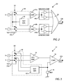
FIG. 2 is a block diagram of an example COMMON MODE fault detector of FIG. 1;
FIG. 3 is a block diagram of an example NOT EQUAL fault detector of FIG. 1;
FIG. 4 is a block diagram of an example POWER SUPPLY fault detector of FIG. 1;
FIG. 5 is a block diagram of an example OUTPUT SHORT fault detector of FIG. 1;
FIG. 6A is a schematic diagram of a first example control circuit of FIG. 1;
FIG. 6B is a schematic diagram of a second example control circuit of FIG. 1;
FIG. 6C is a schematic diagram of a third example control circuit of FIG. 1; and
FIG. 6D is a schematic diagram of a fourth example control circuit of FIG. 1.
DETAILED DESCRIPTION OF EXAMPLE EMBODIMENTS
FIG. 1 is a block diagram, set forth by way of example and not limitation, of an integrated circuit 10 including an analog device such as an operational amplifier (“op-amp”) 12 having a power input 14, an analog device input 16, and an analog device output 18. The example integrated circuit 10 further includes at least one on-line fault detector (e.g. COMMON MODE fault detector 20, NOT EQUAL fault detector 22, POWER SUPPLY (“PS TEST”) fault detector 24, and OUTPUT SHORT fault detector 26), a control circuit 28, a first circuit breaker (“CB # 1”) 30 and a second circuit breaker (“CB # 2”) 32. As will be appreciated by those of skill in the art, more or fewer on-line fault detectors and/or circuit breakers can be provided by integrated circuit 10, as well as other analog and/or digital circuitry.
Integrated circuit 10 includes a semiconductor die 34 which is diced from a semiconductor wafer comprising silicon, gallium arsenide, or other semiconductor material. The semiconductor die is enclosed within an insulating package 36 comprising a plastic, ceramic or other insulating material. The integrated circuit 10 further includes a number of conductive pins 38 ( e.g. pins 38 a, 38 b, 38 c, 38 d and 38 e) comprising metal or a metal alloy which extend through the insulating package 36 and connect to the die 34. In this non-limiting example, pins 38 a and 38 b connect to analog device input 16, pin 38 c connects to circuit breaker 32, pin 38 d connects to a positive power supply voltage Vcc rail of the die 34 and pin 38 e connects to a ground rail of the die 34.
While the current example refers to a single semiconductor die, it is to be understood that in certain embodiments more than one semiconductor die can be provided within a semiconductor package of an integrated circuit. As used herein, a “die” will mean either a single die or multiple dies connected together within a single semiconductor package.
In this non-limiting example, the analog device is an operational amplifier (“op-amp”) 12 and at least one of the on-line fault detectors (e.g. NOT EQUAL fault detector 22) is particularly adapted for use with op-amp 12. However, it will be appreciated by those of skill in the art that analog devices other than op-amp 12 can alternatively be provided on an integrated circuit and monitored by appropriate on-line fault detectors. Op-amp 12 includes a V+ input and a V− input which are connected to pins 38 a and 38 b, respectively, by a differential pair of lines comprising analog input 16.
In this example, the COMMON MODE fault detector 20 and NOT EQUAL fault detector 22 are coupled to analog input 16 and, therefore, to the V+ and V− inputs of op-amp 12. PS TEST fault detector 24 is coupled to power input 14 and OUTPUT SHORT fault detector 26 is coupled to analog device output 18. Furthermore, in this example, each of fault detectors 20, 22, 24 and 26 are coupled to the control circuit 28 by TEST lines 20 a, 22 a, 24 a and 26 a, respectively, and FAULT lines 20 b, 22 b, 24 b and 26 b, respectively. First circuit breaker 30 is coupled between Vcc and power input 14 and second circuit breaker 32 is coupled between analog device output 18 and pin 38 c. The circuit breakers 30 and 32 are coupled to control circuit 28 by CNTL lines 30 a and 32 a, respectively. Control circuit 28 is optionally coupled to one or more pins 38 x by a bus 40 comprising one or more conductive lines. In certain embodiments a bus 40 and pins 38 x are not provided.
FIG. 2 is a block diagram, set forth by way of example and not limitation, of a COMMON MODE fault detector 20 including amplifiers 42 a and 42 b, window comparators 44 a and 44 b, and an OR gate 46. In this example, the COMMON MODE fault detector 20 also includes detector self-test (DST) circuitry 48 including a test generator 50 and a double-pole double-throw (DPDT) electronic switch 52. COMMON MODE fault detector 20 is designed to detect common-mode interference and noise at the two inputs of op-amp 12 by detecting if either of the inputs is outside of its acceptable “window” of voltage levels.
In a normal operational mode, switch 52 couples the V+ input of op-amp 12 to the input of amplifier 42 a and the V− input of op-amp 12 to the input of amplifier 42 b. Outputs of amplifiers 42 a and 42 b are coupled to inputs of window comparators 44 a and 44 b, respectively. The outputs of window comparators 44 a and 44 b are input into OR gate 46 to produce a signal on FAULT line 20 b.
At certain times it is desirable for the control circuitry 28 to activate the DST circuitry 48 by applying a test control signal to TEST line 20 a. For example, a test control signal may be applied upon power-up of the integrated circuit 10. A test control signal can also be applied periodically or sporadically during the operation of integrated circuit 10 or during times when the integrated circuit 10 detects an idle condition. When a test control signal is applied to the TEST line 20 a by control circuitry 28, the switch 20 a is activated and an output of test generator is applied to the inputs of amplifiers 42 a and 42. During the DST process, the COMMON MODE fault detector 20 is uncoupled from the V+ and V− inputs of op-amp 12, which can continue to operate as normal. It will therefore be appreciated that switch 52 selectively couples the window comparators 44 a and 446 to either the V+ and V− inputs of the op-amp 12 or to the test generator 50, in this non-limiting example.
The test generator 50 generates one or more voltage levels to determine if the COMMON MODE fault detector 20 is working properly (e.g. if the upper and lower thresholds of the window comparators are within tolerance levels). Since the control circuitry 28 generated the test control signal that is applied to the TEST line 20 a, it knows that the signal on fault line 20 b is in response to the test voltages produced by test generator 50 and not due to its monitoring of op-amp 12. Also, additional communication lines can be provided between the COMMON MODE fault detector 20 and the control circuitry 28 for more communication or control.
If the control circuitry 28 determines that the COMMON MODE fault detector 20 is not working properly, it can leave it disconnected from the op-amp 12 and/or can provide a signal on bus 40 to alert the system that the COMMON MODE fault detector is not working properly. After the self-test, the test control signal can be removed from the TEST line 20 a and the COMMON MODE fault detector can return to its normal on-line monitoring of the operation of op-amp 12.
FIG. 3 is a block diagram, set forth by way of example and not limitation, of a NOT EQUAL fault detector 22 including a differential amplifier 54, a comparator 56, and a reference voltage 58. In this example, NOT EQUAL fault detector 22 also includes DST circuitry 60 including a double-pole double-throw (DPDT) switch 64 and a test generator 62. The NOT EQUAL fault detector 22 is designed to monitor whether the differential voltage at input 16 is so large as to put the op-amp 12 into saturation. As noted previously, negative feedback is typically used to keep the differential input voltage relatively small. As used herein, “not equal” means that the differential input voltage is very small (e.g. about the offset voltage —the small differential voltage applied to the inputs to force the output to zero).
In a normal operational mode, switch 64 couples the V+ input of op-amp 12 to a first input of differential amplifier 54 and the V− input of op-amp 12 to a second input of the differential amplifier 64. The output of differential amplifier 54 is coupled to a first input of comparator 56 and a second input of comparator 56 is coupled to voltage reference (VREF) 58. The output of comparator 56 is, in this example, the FAULT signal on FAULT line 22 b.
As described about, the NOT EQUAL fault detector 22 can be tested by activating the DST circuitry 60 by applying a Test control signal to TEST line 22 a. In this example, test generator 62 has an input coupled to V REF 58 and two outputs with are coupled to the two inputs of differential amplifier 54 when in a test mode. Switch 64 therefore selectively couples the inputs of the differential amplifier 54 to either the inputs of the op-amp 12 or to the outputs of test generator 58.
The test generator 62 generates one or more voltage levels to determine if the NOT EQUAL fault detector 22 is working properly (e.g. if the differential voltage input to the op-amp 12 is greater than a predetermined limit). Since the control circuitry 28 generated the test control signal that is applied to the TEST line 22 a, it knows that the signal on fault line 22 b is in response to the test voltages produced by test generator 62 and not due to its monitoring of op-amp 12. Also, additional communication lines can be provided between the NOT EQUAL fault detector 22 and the control circuitry 28 for more communication or control.
If the control circuitry 28 determines that the NOT EQUAL fault detector 22 is not working properly, it can leave it disconnected from the op-amp 12 and/or can provide a signal on bus 40 to alert the system that the NOT EQUAL fault detector is not working properly. After the self-test, the test control signal can be removed from the TEST line 22 a and the NOT EQUAL fault detector can return to its normal on-line monitoring of the operation of op-amp 12.
FIG. 4 is a block diagram, set forth by way of example and not limitation, of a POWER SUPPLY fault detector 24 including an offset voltage source 66, a voltage divider 68, a window comparator 70, and an OR gate 72. In this example, offset voltage source 66 includes a voltage reference 74 and a resistor 76 and voltage divider 68 includes a pair of resistors 80 and 78 providing a number of nodes at different voltage levels. In this example, POWER SUPPLY fault detector 24 also includes DST circuitry 82 including a double-pole double-throw (DPDT) switch 84 and a test generator 86.
In a normal operational mode, switch 84 connects Vcc to a node 88 connected to window comparator 70 by a resistor 90. A resistor 91 connects node 88 to ground. A first input to window comparator 70 is coupled to first and second nodes of voltage divider 68. A pair of outputs from window comparator 70 are coupled to inputs of OR gate 72, and a FAULT signal is developed on FAULT line 24 b.
In this example, POWER SUPPLY fault detector 24 can be tested by activating the DST circuitry 60 by applying a Test control signal to TEST line 24 a. Test generator 86 has an output coupled to one of the throws of DPDT switch 84 such that it can be coupled to ground node 88. Switch 84 therefore selectively couples ground node 88 to either Vcc via resistor 90 or to test generator 88.
The test generator 86 generates one or more voltage levels to determine if the POWER SUPPLY fault detector 24 is working properly (e.g. if Vcc is too low or too high). Since the control circuitry 28 generated the test control signal that is applied to the TEST line 24 a, it knows that the signal on fault line 24 b is in response to the test voltages produced by test generator 86 and not due to its monitoring of op-amp 12. Also, additional communication lines can be provided between the POWER SUPPLY fault detector 24 and the control circuitry 28 for more communication or control.
If the control circuitry 28 determines that the POWER SUPPLY fault detector 24 is not working properly, it can leave it disconnected from the op-amp 12 and/or can provide a signal on bus 40 to alert the system that the POWER SUPPLY fault detector is not working properly. After the self-test, the test control signal can be removed from the TEST line 24 a and the POWER SUPPLY fault detector can return to its normal on-line monitoring of the operation of op-amp 12.
FIG. 5 is a block diagram, set forth by way of example and not limitation, of an OUTPUT SHORT fault detector 26 including a pair of voltage dividers 92 and 94, a pair of comparators 96 and 98, and an OR gate 100. Voltage divider 92 is coupled between Vcc and ground and includes resistors 102 and 104. Voltage divider 94 is also coupled between Vcc and ground and includes resistors 106 and 108. A first input to comparator 96 is coupled to a node between resistors 102 and 104 and a first input to comparator 94 is coupled to a node between resistors 106 and 108. In this example, OUTPUT SHORT fault detector 26 further includes DST circuitry 110 including two single-pole double-throw (SPDT) switches 112 a and 112 b.
In a normal operational mode, switch 112 connects output 18 of op-amp 12 to a second input to comparator 96 and to a second input to comparator 98. Outputs of comparators 96 and 98 are connected to inputs of OR gate 100 which develops a FAULT signal on FAULT line 26 b.
In this example, OUTPUT SHORT fault detector 26 can be tested by activating DST circuitry 110 by applying a Test control signal to TEST line 26 a which, in this case, is a bus having a TEST VOLTAGE (TEST V) line and a TEST GROUND (TEST G) line. When a TEST V signal is applied to the TEST V line of TEST line 26 a, SPDT switch 112 a connects the second input of comparator 96 to Vcc. When a TEST G signal is applied to the TEST G line of TEST line 26 a, SPDT switch 112 b connects the second input of comparator 98 to ground.
Unlike the previously discussed fault detectors, this example OUTPUT SHORT fault detector 26 does not use a test generator to produce one or more voltages. This is because the OUTPUT SHORT fault detector is used to detect whether the output of op-amp 12 is either close to Vcc or close ground (each signifying an “output short”). Therefore, comparing Vcc and ground to voltages near to Vcc and ground (from the voltage dividers 92 and 94) with comparators 96 and 98, respectively, provides a test of the proper operation of OUTPUT SHORT fault detector 28.
Since the control circuitry 28 generated the test control signal that is applied to the TEST line 26 a, it knows that the signal on fault line 26 b is in response to output short test and not due to its monitoring of op-amp 12. Also, additional communication lines can be provided between the OUTPUT SHORT fault detector 26 and the control circuitry 28 for more communication or control.
If the control circuitry 28 determines that the OUTPUT SHORT fault detector 26 is not working properly, it can leave it disconnected from the op-amp 12 and/or can provide a signal on bus 40 to alert the system that the OUTPUT SHORT fault detector is not working properly. After the self-test, the test control signal can be removed from the TEST line 26 a and the OUTPUT SHORT fault detector can return to its normal on-line monitoring of the operation of op-amp 12.
FIGS. 6A to 6D illustrate embodiments, set forth by way of example and not limitation, for control circuitry 28 of FIG. 1. In FIG. 6A, control circuitry 28 a includes electrically conductive lines formed in the bus 40, allowing off-chip control and monitoring of integrated circuit 10. This configuration can be advantageous in that it simplifies on-chip circuitry and provide sophisticated off-chip control.
In FIG. 6B, control circuitry includes combinatorial logic 114 such as AND gates, OR gates and inverters. For example, combinational logic 114 can automatically control circuit breaker 30 and/or circuit breaker 32 based upon FAULT signals from the fault detectors 20, 22, 24 and 26. For example, if FAULT lines 24 b are 25 b input into an AND gate, the output of the AND gate can be applied to control lines 30 a and 32 a to open (“trip”) both of circuit breakers 30 and 32. As another example, if FAULT lines 20 b and 22 b are input into an AND gate having an output going to a first input of an OR gate and if FAULT line 24 is input into a second input of the OR gate, the output of the OR gate can be applied to control line 30 to trip circuit breaker 30 if the voltage is out of specification or if a fault is detected by both the COMMON MODE fault detector and the NOT EQUAL fault detector.
It should be noted that combinatorial logic 114 can operate automatically without any off-chip control. In certain example embodiment, bus 40 is not required. In other embodiments bus 40 is provided to, for example, allow configuration of the combinatorial logic (e.g. by burning fuses) or to provide off-chip access to various signals. Advantageously, combinatorial logic is fast, inexpensive, and does not require a clock.
FIGS. 6C and 6D illustrate, by way of example and not limitation, alternative logic for implementing functions of control circuitry 28. More particularly, in FIG. 6C control circuitry 28 c include a state machine 116, and in FIG. 6D control circuitry 28 d includes a microcontroller (or microprocessor) 118. While both state machine 116 and microcontroller 118 require a clock and are generally more complex, they also allow more complex and sophisticated detection, analysis and control of the circuitry. A bus 40 of one or more lines can be provided for off-chip communication with either or both of control circuits 28 c and 28 d, or may be omitted in some embodiments.
It will be appreciated that by monitoring the parameters and proper functioning of analog devices while they are operating (“on-line”) that transient conditions and temporary part failures can be detected real-time and appropriate actions can be taken. It will also be appreciated that the various detectors can be self-tested either while the integrated circuit is operating (“on-line”) or during a special test mode (“off-line”). While the detectors are in the self-testing process, they are disconnected from the analog device that they are monitoring and, as such, the operation of the analog device is unchanged during the self-testing of the detectors.
Although various embodiments have been described using specific terms and devices, such description is for illustrative purposes only. The words used are words of description rather than of limitation. It is to be understood that changes and variations may be made by those of ordinary skill in the art without departing from the spirit or the scope of various inventions supported by the written disclosure and the drawings. In addition, it should be understood that aspects of various other embodiments may be interchanged either in whole or in part. It is therefore intended that the claims be interpreted in accordance with the true spirit and scope of the invention without limitation or estoppel.

Claims (10)

The invention claimed is:
1. An integrated circuit with analog device fault detection comprising:
an integrated circuit die including an operational amplifier (op-amp) having a power input, a V+ input, a V− input and an op-amp output, an on-line fault detector coupled to said V+ input and said V− input and having a fault detector output, and a control circuit coupled to said fault detector and responsive to said fault detector output, wherein said on-line fault detector is a COMMON MODE fault detector including detector self-test (DST) circuitry to test said on-line fault detector and a test input coupled to said control circuit;
an electrically insulating package enclosing said integrated circuit die; and
a number of pins extending through said electrically insulating package and connected to said integrated circuit die;
wherein said COMMON MODE fault detector includes a first window comparator having an input selectively coupled to said V+ input to develop a first fault signal when the voltage on said V+ input is out of a first range and a second window comparator having an input selectively coupled to said V− input which produces a second fault signal when said voltage on said V− input is out of a second range, whereby a fault signal is applied to said fault detector output upon the occurrence of at least one of said first fault signal and said second fault signal.
2. An integrated circuit with analog device fault detection as recited in claim 1 wherein said DST comprises a test generator which selectively applies test signals to said first window comparator and said second window comparator in response to a control signal applied to said test input.
3. An integrated circuit with analog device fault detection comprising:
an integrated circuit die including an operational amplifier (op-amp) having a power input, a V+ input, a V− input and an op-amp output, an on-line fault detector coupled to said V+ input and said V− input and having a fault detector output, and a control circuit coupled to said fault detector and responsive to said fault detector output, wherein said on-line fault detector is a NOT EQUAL detector including detector self-test (DST) circuitry to test said on-line fault detector and including a test input coupled to said control circuit;
an electrically insulating package enclosing said integrated circuit die; and
a number of pins extending through said electrically insulating package and connected to said integrated circuit die.
4. An integrated circuit with analog device fault detection as recited in claim 3 wherein said NOT EQUAL fault detector includes a differential amplifier, a comparator, and a reference voltage, wherein said differential amplifier has a first input selectively coupled to said V+ input and a second input selectively coupled to said V− input, wherein a first input of said comparator is coupled to an output of said differential amplifier and a second input of said comparator is coupled to said reference voltage, and wherein said output of said comparator comprises said fault detector output.
5. An integrated circuit with analog device fault detection as recited in claim 4 wherein said DST comprises a test generator which applies test signals to said differential amplifier in response to a control signal applied to said test input.
6. An integrated circuit with analog device fault detection comprising:
an integrated circuit die including an operational amplifier (op-amp) having a V+ input, a V− input and an op-amp output, a POWER SUPPLY fault detector coupled to said power input and having a fault detector output, and a control circuit coupled to said fault detector and responsive to said fault detector output, wherein said POWER SUPPLY fault detector includes detector self-test (DST) circuitry to test said POWER SUPPLY detector, and has a test input coupled to said control circuit;
an electrically insulating package enclosing said integrated circuit die; and
a number of pins extending through said electrically insulating package and connected to said integrated circuit die;
wherein said POWER SUPPLY fault detector includes a voltage divider having a number of nodes coupled to said op-amp power supply input, a window comparator having a first input coupled to a first node of said voltage divider which produces a first fault signal when a voltage of said op-amp power supply input exceeds a first threshold value and a second input coupled to a second node of said voltage divider which produces a second fault signal when a voltage of said op-amp power supply falls below a second threshold value, whereby a fault signal is applied to said fault detector output upon the occurrence of at least one of said first fault signal and said second fault signal.
7. An integrated circuit with analog device fault detection as recited in claim 6 wherein POWER SUPPLY fault detector further includes a ground input, wherein said DST comprises a test generator which selectively applies test signals to said ground input.
8. An integrated circuit with analog device fault detection comprising:
an integrated circuit die including an analog device having a power input, an analog device input and an analog device output, an OUTPUT SHORT fault detector coupled to said analog device output and having a fault detector output, and a control circuit coupled to said fault detector and responsive to said fault detector output;
an electrically insulating package enclosing said integrated circuit die; and
a number of pins extending through said electrically insulating package and connected to said integrated circuit die;
wherein said OUTPUT SHORT fault detector includes a first voltage divider coupled to a first input of a first comparator and a second voltage divider coupled to a first input of a second comparator, wherein a second input of said first comparator and a second input of said second comparator are selectively coupled to said analog device output, wherein said first comparator provides a first fault signal if said op-amp output is shorted to Vcc, and wherein said second comparator provides a second fault signal if said op-amp output is shorted to ground, whereby a fault signal is applied to said fault detector output upon the occurrence of at least one of said first fault signal and said second fault signal.
9. An integrated circuit with analog device fault detection as recited in claim 8 wherein said integrated circuit die further comprises a first circuit breaker controlled by said control circuit, said first circuit breaker coupling a power supply to said power input.
10. An integrated circuit with analog device fault detection as recited in claim 9 wherein said integrated circuit die further comprises a second circuit breaker controlled by said control circuit, said second circuit breaker coupling said analog device output to a pin of said number of pins.
US13/597,163 2012-08-28 2012-08-28 Integrated circuit with analog device fault detection Active 2033-08-28 US9194884B1 (en)

Priority Applications (2)

Application Number Priority Date Filing Date Title
US13/597,163 US9194884B1 (en) 2012-08-28 2012-08-28 Integrated circuit with analog device fault detection
US14/929,061 US9714971B1 (en) 2012-08-28 2015-10-30 Method for detecting a fault condition of an operational amplifier

Applications Claiming Priority (1)

Application Number Priority Date Filing Date Title
US13/597,163 US9194884B1 (en) 2012-08-28 2012-08-28 Integrated circuit with analog device fault detection

Related Child Applications (1)

Application Number Title Priority Date Filing Date
US14/929,061 Continuation US9714971B1 (en) 2012-08-28 2015-10-30 Method for detecting a fault condition of an operational amplifier

Publications (1)

Publication Number Publication Date
US9194884B1 true US9194884B1 (en) 2015-11-24

Family

ID=54542823

Family Applications (2)

Application Number Title Priority Date Filing Date
US13/597,163 Active 2033-08-28 US9194884B1 (en) 2012-08-28 2012-08-28 Integrated circuit with analog device fault detection
US14/929,061 Active US9714971B1 (en) 2012-08-28 2015-10-30 Method for detecting a fault condition of an operational amplifier

Family Applications After (1)

Application Number Title Priority Date Filing Date
US14/929,061 Active US9714971B1 (en) 2012-08-28 2015-10-30 Method for detecting a fault condition of an operational amplifier

Country Status (1)

Country Link
US (2) US9194884B1 (en)

Cited By (9)

* Cited by examiner, † Cited by third party
Publication number Priority date Publication date Assignee Title
US9714971B1 (en) * 2012-08-28 2017-07-25 Maxim Integrated Products, Inc. Method for detecting a fault condition of an operational amplifier
JP2019078728A (en) * 2017-10-27 2019-05-23 ローム株式会社 Monitoring device
US20190392702A1 (en) * 2017-06-14 2019-12-26 Allegro Microsystems, Llc Sensor Integrated Circuits and Methods for Safety Critical Applications
US10636285B2 (en) * 2017-06-14 2020-04-28 Allegro Microsystems, Llc Sensor integrated circuits and methods for safety critical applications
US10692362B2 (en) 2017-06-14 2020-06-23 Allegro Microsystems, Llc Systems and methods for comparing signal channels having different common mode transient immunity
CN112017477A (en) * 2019-05-30 2020-12-01 三星电子株式会社 Semiconductor device with a plurality of semiconductor chips
US11018635B2 (en) * 2018-08-14 2021-05-25 Nxp Usa, Inc. Embedded test circuitry and method therefor
CN113535618A (en) * 2020-03-29 2021-10-22 马克西姆综合产品公司 System and method for fault detection and reporting through a serial interface transceiver
US11719769B1 (en) 2022-06-14 2023-08-08 Allegro Microsystems, Llc Method and apparatus for sensor signal path diagnostics

Families Citing this family (1)

* Cited by examiner, † Cited by third party
Publication number Priority date Publication date Assignee Title
CN108169610A (en) * 2017-11-29 2018-06-15 国电南瑞科技股份有限公司 A kind of one-phase earthing failure in electric distribution network test method based on Real Time Digital Simulator

Citations (13)

* Cited by examiner, † Cited by third party
Publication number Priority date Publication date Assignee Title
US3945030A (en) * 1973-01-15 1976-03-16 Signetics Corporation Semiconductor structure having contact openings with sloped side walls
US5049764A (en) * 1990-01-25 1991-09-17 North American Philips Corporation, Signetics Div. Active bypass for inhibiting high-frequency supply voltage variations in integrated circuits
US5103188A (en) 1989-08-04 1992-04-07 Gregory Bender Buffered transconductance amplifier
US5585731A (en) 1994-11-01 1996-12-17 Mitsubishi Denki Kabushiki Kaisha Test circuit of current-voltage conversion amplifier
US5771174A (en) * 1995-12-21 1998-06-23 Measurex Corporation Distributed intelligence actuator controller with peer-to-peer actuator communication
CN1193114A (en) * 1998-03-03 1998-09-16 韩熔 On-line detection method for function of operational amplifier
US6104304A (en) * 1999-07-06 2000-08-15 Conexant Systems, Inc. Self-test and status reporting system for microcontroller-controlled devices
US20020014577A1 (en) * 1998-07-08 2002-02-07 Ppt Vision, Inc. Circuit for machine-vision system
US6421214B1 (en) * 2000-03-03 2002-07-16 Pass & Seymour, Inc. Arc fault or ground fault detector with self-test feature
US6426632B1 (en) * 1999-03-29 2002-07-30 George A. Spencer Method and apparatus for testing an AFCI/GFCI circuit breaker
US20030039388A1 (en) * 1998-07-08 2003-02-27 Ulrich Franz W. Machine vision and semiconductor handling
US6624405B1 (en) 1999-04-19 2003-09-23 Capella Microsystems, Inc. BIST for testing a current-voltage conversion amplifier
US7745775B2 (en) 2003-12-15 2010-06-29 International Business Machines Corporation Testing of transimpedance amplifiers

Family Cites Families (6)

* Cited by examiner, † Cited by third party
Publication number Priority date Publication date Assignee Title
US4220833A (en) * 1977-09-12 1980-09-02 The United States Of America As Represented By The Secretary Of The Army Location of a faulty pulse form restorer in a cable system
US5781024A (en) * 1996-07-26 1998-07-14 Diametrics Medical, Inc. Instrument performance verification system
US6556397B2 (en) * 2000-05-12 2003-04-29 Human El-Tech, Inc. Device and method for detecting arc fault
US6433527B1 (en) * 2001-06-01 2002-08-13 Maxim Integrated Products, Inc. Phase failure detector for multi-phase switching regulators
WO2009048619A1 (en) * 2007-10-10 2009-04-16 International Rectifier Corporation Ground fault detection circuit for use in high voltage motor drive applications
US9194884B1 (en) * 2012-08-28 2015-11-24 Maxim Integrated Products, Inc. Integrated circuit with analog device fault detection

Patent Citations (15)

* Cited by examiner, † Cited by third party
Publication number Priority date Publication date Assignee Title
US3945030A (en) * 1973-01-15 1976-03-16 Signetics Corporation Semiconductor structure having contact openings with sloped side walls
US5103188A (en) 1989-08-04 1992-04-07 Gregory Bender Buffered transconductance amplifier
US5049764A (en) * 1990-01-25 1991-09-17 North American Philips Corporation, Signetics Div. Active bypass for inhibiting high-frequency supply voltage variations in integrated circuits
US5049764B1 (en) * 1990-01-25 1992-12-15 G Meyer Robert
US5585731A (en) 1994-11-01 1996-12-17 Mitsubishi Denki Kabushiki Kaisha Test circuit of current-voltage conversion amplifier
US5771174A (en) * 1995-12-21 1998-06-23 Measurex Corporation Distributed intelligence actuator controller with peer-to-peer actuator communication
CN1193114A (en) * 1998-03-03 1998-09-16 韩熔 On-line detection method for function of operational amplifier
US20020014577A1 (en) * 1998-07-08 2002-02-07 Ppt Vision, Inc. Circuit for machine-vision system
US20030039388A1 (en) * 1998-07-08 2003-02-27 Ulrich Franz W. Machine vision and semiconductor handling
US6426632B1 (en) * 1999-03-29 2002-07-30 George A. Spencer Method and apparatus for testing an AFCI/GFCI circuit breaker
US6624405B1 (en) 1999-04-19 2003-09-23 Capella Microsystems, Inc. BIST for testing a current-voltage conversion amplifier
US6104304A (en) * 1999-07-06 2000-08-15 Conexant Systems, Inc. Self-test and status reporting system for microcontroller-controlled devices
US6421214B1 (en) * 2000-03-03 2002-07-16 Pass & Seymour, Inc. Arc fault or ground fault detector with self-test feature
US7745775B2 (en) 2003-12-15 2010-06-29 International Business Machines Corporation Testing of transimpedance amplifiers
US7977618B2 (en) 2003-12-15 2011-07-12 International Business Machines Corporation Testing of transimpedance amplifiers

Non-Patent Citations (10)

* Cited by examiner, † Cited by third party
Title
Maxim Integrated Products, "1mm × 1mm Video Filter Amplifier with Automatic Shutdown and 2V/V Gain," Data Sheet, MAX9515, Maxim Integrated Products, 19-3214; Rev 1; Aug. 2008, pp. 1-10.
Maxim Integrated Products, "1mm × 1mm Video Filter Amplifier with Automatic Shutdown and 4V/V Gain," Data Sheet, MAX9519, Maxim Integrated Products, 19-4231; Rev 0; Aug. 2008, pp. 1-9.
Maxim Integrated Products, "1muA Supply Current, 1 Mbps, 3.0V to 5.5V, RS-232 Transceivers with AutoShutdown Plus," Data Sheet, MAX3224-MAX3227/MAX3244/MAX3245, Maxim Integrated Products, 19-1289; Rev 5; Feb. 2011, pp. 1-19.
Maxim Integrated Products, "1μA Supply Current, 1 Mbps, 3.0V to 5.5V, RS-232 Transceivers with AutoShutdown Plus," Data Sheet, MAX3224-MAX3227/MAX3244/MAX3245, Maxim Integrated Products, 19-1289; Rev 5; Feb. 2011, pp. 1-19.
Maxim Integrated Products, "AutoShutdown(TM) for Speaker Amplifier Conserves Cell-Phone Power," Application Note 3612, Maxim Integrated Products, Sep. 16, 2005, pp. 1-2.
Maxim Integrated Products, "AutoShutdown™ for Speaker Amplifier Conserves Cell-Phone Power," Application Note 3612, Maxim Integrated Products, Sep. 16, 2005, pp. 1-2.
National Semiconductor Corp., "Zero-Drift, Programmable Instrumentation Amplifier with Diagnostics," Data Sheet, LMP8358, National Semiconductor Corp., May 5, 2010, pp. 1-34.
Regan, Tim, "Comparator Circuit Provides Automatic Shutdown of the LT1795 High Speed ADSL Power Amplifier," Linear Technology Magazine, Sep. 1999, pp. 33-34.
Saluja, Kewal K. et al., "A Concurrent Testing Technique for Digital Circuits," IEEE Transactions on Computer-Aided Design, vol. 7, No. 12, Dec. 1988 IEEE, pp. 1250-1260.
Stout, Mike, "Detecting Faults Between a Sensor and an Amplifier," Electronic Design, Dec. 21, 2010, pp. 1-8.

Cited By (14)

* Cited by examiner, † Cited by third party
Publication number Priority date Publication date Assignee Title
US9714971B1 (en) * 2012-08-28 2017-07-25 Maxim Integrated Products, Inc. Method for detecting a fault condition of an operational amplifier
US20190392702A1 (en) * 2017-06-14 2019-12-26 Allegro Microsystems, Llc Sensor Integrated Circuits and Methods for Safety Critical Applications
US10580289B2 (en) * 2017-06-14 2020-03-03 Allegro Microsystems, Llc Sensor integrated circuits and methods for safety critical applications
US10636285B2 (en) * 2017-06-14 2020-04-28 Allegro Microsystems, Llc Sensor integrated circuits and methods for safety critical applications
US10692362B2 (en) 2017-06-14 2020-06-23 Allegro Microsystems, Llc Systems and methods for comparing signal channels having different common mode transient immunity
JP2019078728A (en) * 2017-10-27 2019-05-23 ローム株式会社 Monitoring device
JP7010663B2 (en) 2017-10-27 2022-01-26 ローム株式会社 Monitoring device
US11018635B2 (en) * 2018-08-14 2021-05-25 Nxp Usa, Inc. Embedded test circuitry and method therefor
CN112017477A (en) * 2019-05-30 2020-12-01 三星电子株式会社 Semiconductor device with a plurality of semiconductor chips
US10951348B2 (en) * 2019-05-30 2021-03-16 Samsung Electronics Co., Ltd. Semiconductor devices
US11239937B2 (en) * 2019-05-30 2022-02-01 Samsung Electronics Co., Ltd. Semiconductor devices
CN113535618A (en) * 2020-03-29 2021-10-22 马克西姆综合产品公司 System and method for fault detection and reporting through a serial interface transceiver
CN113535618B (en) * 2020-03-29 2023-08-22 马克西姆综合产品公司 System and method for fault detection and reporting through serial interface transceiver
US11719769B1 (en) 2022-06-14 2023-08-08 Allegro Microsystems, Llc Method and apparatus for sensor signal path diagnostics

Also Published As

Publication number Publication date
US9714971B1 (en) 2017-07-25

Similar Documents

Publication Publication Date Title
US9714971B1 (en) Method for detecting a fault condition of an operational amplifier
US7609080B2 (en) Voltage fault detection and protection
US7859287B2 (en) Device power supply extension circuit, test system including the same and method of testing semiconductor devices
US8896975B2 (en) Voltage regulator over-voltage detection system, method and apparatus
KR20070021804A (en) Temperature detector, temperature detecting method, and semiconductor device having the temperature detector
US8280670B2 (en) Method and apparatus for detecting failure of an actuator switching device
US10187052B2 (en) Device and method for internal reset signal generation
JP2010210238A (en) Probe card, semiconductor inspection device equipped with the same and method for checking fuse of probe card
KR100851147B1 (en) a dual power system using smart junction box and a line short detection method of the system
US9645192B2 (en) Ground fault circuit interrupter and method
CN110958002B (en) Solid state power switching device
KR101724551B1 (en) Semiconductor test device interface board
US9891277B2 (en) Secure low voltage testing
US6469538B1 (en) Current monitoring and latchup detection circuit and method of operation
US11550348B2 (en) Methods and devices for bypassing a voltage regulator
US10128738B2 (en) Determination of entering and exiting safe mode
JP4641643B2 (en) Delay circuit
KR100647473B1 (en) Multi chip package semiconductor device and method for detecting fail thereof
US7224198B2 (en) Input and output circuit and method of operation thereof
JP5391955B2 (en) Semiconductor device
US20180210027A1 (en) Semiconductor device testing
US9690643B2 (en) Engine-control computer and method for detecting failures of such a computer
KR100614646B1 (en) Built-in current sensor and current testing method thereof
KR20100049755A (en) Semiconductor chip open test circuit and semiconductor chip test system including the same
KR100352032B1 (en) Ic testing device

Legal Events

Date Code Title Description
AS Assignment

Owner name: MAXIM INTEGRATED PRODUCTS, INC., CALIFORNIA

Free format text: ASSIGNMENT OF ASSIGNORS INTEREST;ASSIGNORS:MOSSMAN, JOHN A.;MCCARTHY, ROBERT A.;SIGNING DATES FROM 20121003 TO 20121102;REEL/FRAME:029299/0764

STCF Information on status: patent grant

Free format text: PATENTED CASE

MAFP Maintenance fee payment

Free format text: PAYMENT OF MAINTENANCE FEE, 4TH YEAR, LARGE ENTITY (ORIGINAL EVENT CODE: M1551); ENTITY STATUS OF PATENT OWNER: LARGE ENTITY

Year of fee payment: 4

MAFP Maintenance fee payment

Free format text: PAYMENT OF MAINTENANCE FEE, 8TH YEAR, LARGE ENTITY (ORIGINAL EVENT CODE: M1552); ENTITY STATUS OF PATENT OWNER: LARGE ENTITY

Year of fee payment: 8