US9166527B2 - Amplification circuit having optimization of power - Google Patents
Amplification circuit having optimization of power Download PDFInfo
- Publication number
- US9166527B2 US9166527B2 US13/996,758 US201213996758A US9166527B2 US 9166527 B2 US9166527 B2 US 9166527B2 US 201213996758 A US201213996758 A US 201213996758A US 9166527 B2 US9166527 B2 US 9166527B2
- Authority
- US
- United States
- Prior art keywords
- transistor
- source
- gate
- cascode
- drain
- Prior art date
- Legal status (The legal status is an assumption and is not a legal conclusion. Google has not performed a legal analysis and makes no representation as to the accuracy of the status listed.)
- Expired - Fee Related, expires
Links
- 230000003321 amplification Effects 0.000 title claims abstract description 30
- 238000003199 nucleic acid amplification method Methods 0.000 title claims abstract description 30
- 238000005457 optimization Methods 0.000 title 1
- 239000003990 capacitor Substances 0.000 claims description 12
- 238000012935 Averaging Methods 0.000 claims description 5
- 230000006835 compression Effects 0.000 claims description 5
- 238000007906 compression Methods 0.000 claims description 5
- 238000004891 communication Methods 0.000 claims description 4
- 230000007423 decrease Effects 0.000 claims description 4
- 238000009499 grossing Methods 0.000 claims description 2
- 230000003213 activating effect Effects 0.000 abstract description 2
- 241001125929 Trisopterus luscus Species 0.000 description 6
- 230000006399 behavior Effects 0.000 description 3
- 238000013461 design Methods 0.000 description 3
- 238000000034 method Methods 0.000 description 3
- 230000003044 adaptive effect Effects 0.000 description 2
- 238000010276 construction Methods 0.000 description 1
- 230000000593 degrading effect Effects 0.000 description 1
- 238000001514 detection method Methods 0.000 description 1
- 238000011161 development Methods 0.000 description 1
- 238000005516 engineering process Methods 0.000 description 1
- 238000010295 mobile communication Methods 0.000 description 1
- 230000004044 response Effects 0.000 description 1
- 238000004088 simulation Methods 0.000 description 1
Images


Classifications
-
- H—ELECTRICITY
- H03—ELECTRONIC CIRCUITRY
- H03F—AMPLIFIERS
- H03F1/00—Details of amplifiers with only discharge tubes, only semiconductor devices or only unspecified devices as amplifying elements
- H03F1/02—Modifications of amplifiers to raise the efficiency, e.g. gliding Class A stages, use of an auxiliary oscillation
- H03F1/0205—Modifications of amplifiers to raise the efficiency, e.g. gliding Class A stages, use of an auxiliary oscillation in transistor amplifiers
- H03F1/0277—Selecting one or more amplifiers from a plurality of amplifiers
-
- H—ELECTRICITY
- H03—ELECTRONIC CIRCUITRY
- H03F—AMPLIFIERS
- H03F3/00—Amplifiers with only discharge tubes or only semiconductor devices as amplifying elements
- H03F3/189—High frequency amplifiers, e.g. radio frequency amplifiers
- H03F3/19—High frequency amplifiers, e.g. radio frequency amplifiers with semiconductor devices only
- H03F3/193—High frequency amplifiers, e.g. radio frequency amplifiers with semiconductor devices only with field-effect devices
-
- H—ELECTRICITY
- H03—ELECTRONIC CIRCUITRY
- H03F—AMPLIFIERS
- H03F3/00—Amplifiers with only discharge tubes or only semiconductor devices as amplifying elements
- H03F3/20—Power amplifiers, e.g. Class B amplifiers, Class C amplifiers
- H03F3/21—Power amplifiers, e.g. Class B amplifiers, Class C amplifiers with semiconductor devices only
- H03F3/211—Power amplifiers, e.g. Class B amplifiers, Class C amplifiers with semiconductor devices only using a combination of several amplifiers
-
- H—ELECTRICITY
- H03—ELECTRONIC CIRCUITRY
- H03F—AMPLIFIERS
- H03F3/00—Amplifiers with only discharge tubes or only semiconductor devices as amplifying elements
- H03F3/72—Gated amplifiers, i.e. amplifiers which are rendered operative or inoperative by means of a control signal
-
- H—ELECTRICITY
- H03—ELECTRONIC CIRCUITRY
- H03F—AMPLIFIERS
- H03F2200/00—Indexing scheme relating to amplifiers
- H03F2200/453—Controlling being realised by adding a replica circuit or by using one among multiple identical circuits as a replica circuit
Definitions
- the invention relates to power amplifiers and more particularly to a Class AB power amplification which offers good linearity and low current consumption.
- FIG. 1 Another simple structure which is known is based on the class AB power amplifier having an input 6 and an output 7 , such as illustrated in FIG. 1 , which comprises a MOS transistor 1 having a gate receiving, through a capacitor 4 an input signal Vin (RFinput) and a drain connected to a Vdd voltage via an inductor 2 and also connected to the RF out output terminal 7 (driving a load ZL 5 ) via an output capacitor 3 .
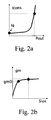
- FIGS. 2 a and 2 b are flow charts respectively illustrating both the current consumption I cons (as a function of the output power P Pout ) and the gain G m of such amplifier depending on the size of the transistor. It can be seen that the current consumption follows a curve that is function of the input RF swing as presented in FIG. 1 .
- a load ZL is determined and I cons is then mainly driven by P out .
- the quiescent current I q has been represented in FIG. 2 a and corresponds to the point of no or little RF input signal. This particular point is determined by an appropriate biasing circuit (not illustrated in FIG. 2 ) which is DC set regarding bias point at G and transistors size.
- the Power Gain (PG) is mainly given by the ratio between the output voltage and the input voltage. Typically PG is around 8-10 dB. Moreover, because of a possible “oversizing”, the typical gain (or gm) for a MOS transistor is not linear anymore with the size, as illustrated in FIG. 2 b , especially once the cell is sized for current.
- the power amplifier is sized at high power but not at low power which represents 80% of the time.
- the designers may decide to (over)size the transistor so as to generate a high amount of power P out , thus increasing the value of the quiescent current I q .
- a power amplifier circuit comprising:
- the total size of the amplification components can be adapted to the value of the output power to generate.
- each of the second transistor is biased, when activated by the control circuit, in class AB showing a quiescent current Iq.
- the sensing means comprises:
- the invention also achieves a power amplification circuit comprising
- the a third transistor is mounted as a cascode transistor on the top of both first and second transistors.
- the invention is adapted to the design of a RF amplification circuit for wireless communications and particularly useful for realizing a mobile telephone.
- FIG. 1 illustrates the basic structure of a RF power amplification structure.
- FIGS. 2 a and 2 b are flow charts illustrating both the current Icons and the gain Gm of the amplifier of FIG. 1 .
- FIGS. 3 a and 3 b illustrate the general principle of a so-called Deep Class AB Cascode Power amplifier based on a “variable size” transistor.
- FIG. 4 illustrates a first embodiment of a Deep Class AB cascode Power amplifier using adaptive control of the size of the transistor in response to the input voltage.
- FIGS. 5 a and 5 b illustrate the result of a simulation for a 2.5 Ghz power amplifier.
- FIG. 6 gives the power distribution of an OFDM signal.
- FIGS. 7 and 8 illustrate a second embodiment and gives the consumption profile of a deep Class AB PA with a high size together with the one of a Class A PA with a lower size.
- FIG. 9 shows the second embodiment wherein both Class A and Class AB structures are merged together.
- FIG. 10 illustrates the second embodiment with the cascode transistor
- FIG. 11 illustrates the efficiency of the Power Amplifier of the pure ClassAB PA and the one using the structure. One may notice that there is almost no difference
- FIG. 12 gives the linearity of the pure ClassAB PA and the one using the structure. The linearity is far better using the structure. At medium power (Pout from 10 to 16 dBm) EVM is up to 10 dB better. At high power, EVM is the same but mask is improved.
- GND will refer to a first reference voltage and Vdd is a second reference voltage which may correspond to either a positive voltage or a negative voltage, thus determining the particular type of the transistor to consider. For instance, when Vdd is a positive voltage, the MOS transistors will be NMOS transistors while, if Vdd correspond to a negative voltage, PMOS transistors will have to be considered.
- the embodiments described below are particularly adapted to the design of Radio Frequency amplification circuits used in modern mobile telecommunication equipments, requiring a high degree of linearity, together with a low consumption of current.
- a new amplification circuit illustrated in FIG. 3 , and including one specific component, shown as a “variable” transistor, e.g. of a a ‘variable size” transistor 10 allowing adaptive control of its size in accordance with the output power which is desired.
- such “variable size” transistor when used in a Class AB structure, allows to take advantage of different Icons (Pout) curves so as to leave the operating point on the tangent shown in FIG. 3 b , thus optimizing the power consumption and the output power.
- the size of “transistor” 10 is varied, in a controllable way, with the targeted power. More particularly, there is included control means for increasing the size of transistor 10 with the reaching of a percentage of Iq (Icons), which is given by linearity consideration (limit between deep Class AB and ClassAB for instance)
- I cons is an image of Output Power (and input one at large signal), so I cons is in phase with output swing.
- Two particular embodiments will be particularly considered, a first embodiment taking advantage of a series of MOS transistors coupled in parallel and all biased in Class AB structures (I) and a second embodiment (II) showing the combination of a MOS transistor biased in class AB and combined with a class A structure.
- FIG. 4 illustrates one embodiment of a class AB cascode amplification circuit using a series of MOS transistors.
- the circuit comprises an input 100 receiving the input signal and connected to a first input of a capacitor 101 having a second input connected to the gate (G 0 ) of a transistor MO 102 and also to the gate (G 1 , G 2 , . . . Gn) of a series of n MOS transistors 110 - 1 to 110 - n , the source of which being connected to a reference voltage Gnd.
- Transistors M 1 -Mn have their drains which are respectively connected to the source of an associated transistors 120 - 1 - 120 - n , the drain of which being connected to the output of the amplifier, that is to say to a first input of an inductor 140 having a second input connected to reference voltage Vdd, and also to a first input of capacitor 160 , the second input of which being connected to an output 700 (Rfout) and to the load ZL 5 . Therefore, the amplification circuit comprises a set of n cascode circuits, each cascode circuit comprising a first transistor ( 110 - 1 , 110 - 2 , . . . 110 - n ) and a second transistor ( 120 - 1 , 120 - 2 , . . . 120 - n ).
- Sensing circuit 130 includes a first branch two resistors 131 and 132 connected in series between the reference voltage Vdd and the drain of transistor Mc 0 103 .
- the voltage across one of the two resistors connected in series, namely resistor 132 is sensed and forwarded to a control unit 150 (so-called Droop circuit), having a set of output lends which are coupled to the gates Gc 1 , Gc 2 . . . Gcn of the sequence of NMOS transistors 120 - 1 , 120 - 2 . . . 120 - n
- the system will sense the I q depending on RFin and choose the right size of the variable PA in order to optimize the Efficiency of the Power Amplifier (PAE).
- a connection to power detection control loop can help also the system.
- the TOP schematic is presented in FIG. 5 b . It includes a Current sensor 510 , a Level detector 520 , a Biasing switch 530 , and a switchable size PA.
- sensing of the current is based on the use of 2 or more transistors (eg transistors 102 and 103 ) functioning in RF that receive an image of the input signal applied to the total PA.
- Sensing circuit 130 comprising resistor 132 and a capacitor 133 serves for averaging the signal at the drain of the sense transistor 103 , gives a dc value of the quiescent current of this transistor versus the input power.
- This signal is transferred to control circuit 150 comprising a bank of comparators for creating e steps and control the size of the final PA being equivalent to the structure formed of transistors M 1 -Mn.
- FIG. 7 presents the main results which can be obtained with the first embodiment.
- the current consumption at low output power is reduced compared to the one of conventional stage.
- the impact on the input impedance matching is very small.
- the system keeps the performances of the conventional PA.
- the first embodiment advantageously saves power consumption at low power for ClassAB PA.
- it takes small area and can be implemented in pure CMOS technology.
- the second embodiment which is described below is particularly adapted for handling the more recent modulation techniques, having high PAPR (Peak to Average Power Ratio) (6-10 dB), and which require very good linearity combined with low power consumption as well.
- PAPR Peak to Average Power Ratio
- twin power amplifier which takes advantage of the property of an OFDM signal having a high PAPR to statistically distribute the power around Pout average and up to Pout maximum, as illustrated in FIG. 6 . Even if all the Power is transferred by the PA, most of the linear information is at low power while the consumption should be low at high power.
- FIGS. 7 and 8 gives the consumption profile of a deep Class AB PA with a high size together with the one of a Class A PA with a lower size. Since the Class A size is low the Iq can be low but still providing the right output signal (Vout versus Vin). In a same way, since the Class AB size is high but biasing low (VG on the fig) the quiescent is low. When the input signal increases, its dc current increases and also its gain (expansion) providing a good Vout (once Vin is high enough)
- FIG. 7 representing two power amplifiers, respectively a deep Class AB power amplifier and a class A amplifier
- a deep Class AB power amplifier and a class A amplifier
- the input signal is low and a small ClassA PA is sufficient to provide the gain with a great linearity and without consuming too much.
- a Class AB is preferable to provide this power with low consumption.
- the linearity is mainly driven by signals at lower power which are “boosted” by the Class A biasing.
- FIG. 8 more particularly illustrates the current I cons for the two amplifiers.
- the consumption profile of a deep Class AB PA with a high size together with the one of a Class A PA with a lower size. Since the Class A size is low the Iq can be low but still providing the right output signal (Vout versus Vin). In a same way, since the Class AB size is high but biasing low (VG on the fig) the quiescent is low.
- VG on the fig biasing low
- the quiescent is low.
- the input signal increases, its dc current increases and also its gain (expansion) providing a good Vout (once Vin is high enough)
- FIG. 9 shows two MOS transistors 800 and 900 , respectively having lower and higher size and their source connected to Ground, driving a load ZL 5 via a capacitor 3 and also an inductor 2 connected between Vdd and the drain of both transistors.
- lower size MOS transistor M 1 is biased in class A and receives the RF input at its gate via a capacitor 801 .
- MOS transistor M 2 is biased in Class AB and also receives the RF input at its gate via a capacitor 901 .
- the ClassA and AB are merged together.
- the ClassAB contribution increases while Vout from Class A decreases (compression).
- the total gain is smoothed.
- the twin structure of FIG. 9 thus includes 2 transistors connected by Drain and Source, with 2 different sizes and biased by 2 different networks, the determination of the sizes and the biasing networks being performed by taking into consideration the modulated shape and PAPR to optimize both linearity and consumption.
- the Class A part with, for instance 1 ⁇ 3 of the total area, the remaining 2 ⁇ 3 being allocated to the Class AB part.
- the biasing points also in an opposite ratio. Doing this, if the Class A part with 1 ⁇ 3 of the total area (so 1 ⁇ 3 of the total Gain (gm)) has a high biasing point, its contribution to the gain is high. A Class A PA has a gain proportional to the biasing point. Now, if the Class AB part which represents 2 ⁇ 3 of the total area, so 2 ⁇ 3 of the total available gain, has a lower biasing point, this part will have a lower gain than the maximum available gain (given by the area).
- a twin power amplifier (the same elements already discussed in FIG. 9 keeping the same references) which further includes a third transistor M 3 1000 which has the drain and source connected in series between the drain of transistors 800 and 900 and the output lead.
- Transistor M 3 which is located on the top of the combination (cascode) is used to combine and isolate each structure from load variation ensuring better linearity.
- the output capacitance of a MOS transistor is a function of power. This capacitance is non linear and should be reduced and/or compensated. This is the goal of the output matching network.
- the Class AB contribution is low when input power is low, its capacitance will be low.
- FIG. 11 gives the PAE of the pure ClassAB PA and the one using the structure. One may notice that there is almost no difference
- FIG. 12 gives the linearity of the pure ClassAB PA and the one using the structure. The linearity is far better using the structure. At medium power (Pout from 10 to 16 dBm) EVM is up to 10 dB better. At high power, EVM is the same but mask is improved.
Abstract
-
- means for sensing the input voltage; and
- a set of n cascode circuits, each comprising a first transistor having a gate, a source and a drain terminal and further comprising a second transistor having gate, source and drain terminal; the source and gate of the first transistor of said cascode circuits being respectively connected to a first reference voltage and to receive the input signal, the drain of said first transistor being connected to the source of said second transistor, the drain of which being coupled to said output.
Description
-
- means for sensing the input voltage;
- a set of n cascode circuits, each comprising a first transistor having a gate, a source and a drain terminal and further comprising a second transistor having gate, source and drain terminal; the source and gate of the first transistor of said cascode circuits being respectively connected to a first reference voltage (GND) and to receive the input signal (RFin), the drain of said first transistor being connected to the source of said second transistor, the drain of which being coupled to the output;
- a control circuit receiving the input voltage sensed by the sensing means for generating a set of control signals which are transmitted to the gates of the second transistors of said n cascode circuits;
-
- an additional cascode circuit a first transistor having a gate, a source and a drain terminal and further comprising a second transistor having gate, source and drain terminal; the source and gate of the first transistor of said cascode circuits being being respectively connected to the reference voltage (GND) and to receive the input signal (RFin), the drain of the first transistor being coupled to the source of the second transistor,
- a passive circuit coupled between a second reference voltage (Vdd) and the drain of said second transistor of said additional cascode circuit, the passive circuit comprising two resistors mounted as a voltage divider and, in parallel, one capacitor for averaging the RF signal sensed by said sensing means.
-
- a first MOS transistor having a lower size and biased in class AB amplification, having a gate, source and drain terminal, the source being connected to the ground and the gate being coupled to receive the input signal;
- a second MOS transistor having a higher size and biased in class A, having a gate, source and drain terminals, the source being connected to the ground and the gate being coupled to receive the input signal;
the drains of said first and said second MOS transistor being coupled together to generate the output current to drive the load of said power amplification circuit;
whereby when the input signal increases the ClassAB contribution increases while Vout from Class A decreases (compression), thus smoothing the total gain of said power amplification circuit.
Claims (12)
Priority Applications (1)
| Application Number | Priority Date | Filing Date | Title |
|---|---|---|---|
| US13/996,758 US9166527B2 (en) | 2011-01-27 | 2012-01-26 | Amplification circuit having optimization of power |
Applications Claiming Priority (6)
| Application Number | Priority Date | Filing Date | Title |
|---|---|---|---|
| EP11368002.9 | 2011-01-27 | ||
| EP11368002 | 2011-01-27 | ||
| EP11368002.9A EP2482449B1 (en) | 2011-01-27 | 2011-01-27 | Amplification circuit having optimization of power |
| US201161454076P | 2011-03-18 | 2011-03-18 | |
| PCT/EP2012/000351 WO2012100947A1 (en) | 2011-01-27 | 2012-01-26 | Amplification circuit having optimization of power |
| US13/996,758 US9166527B2 (en) | 2011-01-27 | 2012-01-26 | Amplification circuit having optimization of power |
Publications (2)
| Publication Number | Publication Date |
|---|---|
| US20140197893A1 US20140197893A1 (en) | 2014-07-17 |
| US9166527B2 true US9166527B2 (en) | 2015-10-20 |
Family
ID=44118468
Family Applications (1)
| Application Number | Title | Priority Date | Filing Date |
|---|---|---|---|
| US13/996,758 Expired - Fee Related US9166527B2 (en) | 2011-01-27 | 2012-01-26 | Amplification circuit having optimization of power |
Country Status (3)
| Country | Link |
|---|---|
| US (1) | US9166527B2 (en) |
| EP (2) | EP3499713A1 (en) |
| WO (1) | WO2012100947A1 (en) |
Families Citing this family (5)
| Publication number | Priority date | Publication date | Assignee | Title |
|---|---|---|---|---|
| US9712125B2 (en) | 2015-02-15 | 2017-07-18 | Skyworks Solutions, Inc. | Power amplification system with shared common base biasing |
| WO2018002978A1 (en) * | 2016-06-27 | 2018-01-04 | 三菱電機株式会社 | Power amplifier and variable-gain amplifier |
| CN107132548B (en) * | 2017-06-22 | 2023-07-25 | 中国人民解放军第六九O五工厂 | Amplifying circuit for Beidou search and rescue device |
| TWI706631B (en) * | 2019-11-14 | 2020-10-01 | 財團法人工業技術研究院 | Distributed amplifier with low supply voltage and low power consumption for full-chip high-speed communication |
| CN117579007B (en) * | 2024-01-17 | 2024-04-09 | 成都嘉纳海威科技有限责任公司 | Ultra-wideband dynamic range amplifying and attenuating multifunctional chip |
Citations (11)
| Publication number | Priority date | Publication date | Assignee | Title |
|---|---|---|---|---|
| US4458213A (en) | 1982-12-13 | 1984-07-03 | Sony Corporation | Constant quiescent current, class AB amplifier output stage |
| US6448616B1 (en) | 2001-08-14 | 2002-09-10 | Telefonaktiebolaget Lm Ericsson | Adaptive biasing of RF power transistors |
| US6501334B1 (en) | 2000-11-13 | 2002-12-31 | Texas Instruments Incorporated | Actively biased class AB output stage with low quiescent power, high output current drive and wide output voltage swing |
| US20050225392A1 (en) | 2004-04-07 | 2005-10-13 | Texas Instruments Incorporated | Class AB output stage circuit with stable quiescent current |
| EP1858161A1 (en) | 2006-05-19 | 2007-11-21 | Broadcom Corporation | Dual power mode transmitter |
| EP1993200A1 (en) | 2007-05-08 | 2008-11-19 | EM Microelectronic-Marin SA | Power amplifier with controlled output power |
| WO2009009652A2 (en) | 2007-07-11 | 2009-01-15 | Axiom Microdevices, Inc. | Segmented power amplifier |
| US20100141337A1 (en) | 2008-12-10 | 2010-06-10 | Qualcomm Incorporated | Amplifier with programmable off voltage |
| US20100279641A1 (en) | 2008-12-31 | 2010-11-04 | Siu-Chuang Ivan Lu | Receiver for wireless communication system |
| US8150343B2 (en) * | 2009-09-21 | 2012-04-03 | Broadcom Corporation | Dynamic stability, gain, efficiency and impedance control in a linear/non-linear CMOS power amplifier |
| US8188788B2 (en) * | 2010-04-23 | 2012-05-29 | Samsung Electro-Mechanics | Systems and methods for a discrete resizing of power devices with concurrent power combining structure for radio frequency power amplifier |
Family Cites Families (1)
| Publication number | Priority date | Publication date | Assignee | Title |
|---|---|---|---|---|
| WO2009155010A2 (en) * | 2008-05-27 | 2009-12-23 | Rayspan Corporation | Rf power amplifiers with linearization |
-
2011
- 2011-01-27 EP EP19155202.5A patent/EP3499713A1/en not_active Withdrawn
- 2011-01-27 EP EP11368002.9A patent/EP2482449B1/en active Active
-
2012
- 2012-01-26 WO PCT/EP2012/000351 patent/WO2012100947A1/en active Application Filing
- 2012-01-26 US US13/996,758 patent/US9166527B2/en not_active Expired - Fee Related
Patent Citations (11)
| Publication number | Priority date | Publication date | Assignee | Title |
|---|---|---|---|---|
| US4458213A (en) | 1982-12-13 | 1984-07-03 | Sony Corporation | Constant quiescent current, class AB amplifier output stage |
| US6501334B1 (en) | 2000-11-13 | 2002-12-31 | Texas Instruments Incorporated | Actively biased class AB output stage with low quiescent power, high output current drive and wide output voltage swing |
| US6448616B1 (en) | 2001-08-14 | 2002-09-10 | Telefonaktiebolaget Lm Ericsson | Adaptive biasing of RF power transistors |
| US20050225392A1 (en) | 2004-04-07 | 2005-10-13 | Texas Instruments Incorporated | Class AB output stage circuit with stable quiescent current |
| EP1858161A1 (en) | 2006-05-19 | 2007-11-21 | Broadcom Corporation | Dual power mode transmitter |
| EP1993200A1 (en) | 2007-05-08 | 2008-11-19 | EM Microelectronic-Marin SA | Power amplifier with controlled output power |
| WO2009009652A2 (en) | 2007-07-11 | 2009-01-15 | Axiom Microdevices, Inc. | Segmented power amplifier |
| US20100141337A1 (en) | 2008-12-10 | 2010-06-10 | Qualcomm Incorporated | Amplifier with programmable off voltage |
| US20100279641A1 (en) | 2008-12-31 | 2010-11-04 | Siu-Chuang Ivan Lu | Receiver for wireless communication system |
| US8150343B2 (en) * | 2009-09-21 | 2012-04-03 | Broadcom Corporation | Dynamic stability, gain, efficiency and impedance control in a linear/non-linear CMOS power amplifier |
| US8188788B2 (en) * | 2010-04-23 | 2012-05-29 | Samsung Electro-Mechanics | Systems and methods for a discrete resizing of power devices with concurrent power combining structure for radio frequency power amplifier |
Non-Patent Citations (1)
| Title |
|---|
| International Search Report issued in corresponding International application No. PCT/EP2012/000351, date of mailing Apr. 4, 2012. |
Also Published As
| Publication number | Publication date |
|---|---|
| US20140197893A1 (en) | 2014-07-17 |
| EP3499713A1 (en) | 2019-06-19 |
| WO2012100947A1 (en) | 2012-08-02 |
| EP2482449A1 (en) | 2012-08-01 |
| EP2482449B1 (en) | 2019-03-20 |
Similar Documents
| Publication | Publication Date | Title |
|---|---|---|
| Sowlati et al. | A 2.4-GHz 0.18-μm CMOS self-biased cascode power amplifier | |
| JP4792273B2 (en) | amplifier | |
| US7414479B2 (en) | Automatic bias control circuit for reduced current consumption in a linear power amplifier | |
| EP1620942B1 (en) | Rf amplifier employing active load linearization | |
| US9602059B2 (en) | Amplifier topology for envelope tracking | |
| Sowlati et al. | A 2.4 GHz 0.18/spl mu/m CMOS self-biased cascode power amplifier with 23 dBm output power | |
| US9166527B2 (en) | Amplification circuit having optimization of power | |
| US20090072905A1 (en) | Variable gain amplifier having wide gain variation and wide bandwidth | |
| US8665023B2 (en) | Class-AB/B amplifier with quiescent control circuit | |
| Lollio et al. | A class-G headphone amplifier in 65 nm CMOS technology | |
| CN105379109A (en) | Efficient power amplification over large operating average power range | |
| JP2013236410A (en) | Variable gain amplifier | |
| JPWO2006006244A1 (en) | High power amplifier | |
| KR101498786B1 (en) | Power amplifier | |
| TW201406057A (en) | Cascode amplifier and amplifier circuit | |
| US7298211B2 (en) | Power amplifying apparatus | |
| US7368995B2 (en) | Power amplifier with active bias circuit | |
| Oh et al. | A fully-integrated+ 23-dBm CMOS triple cascode linear power amplifier with inner-parallel power control scheme | |
| JP2019205006A (en) | Power amplifier circuit | |
| JP5757362B2 (en) | High frequency amplifier circuit, wireless device | |
| KR101902381B1 (en) | Linear power amplification circuit using class-c power amplifier | |
| Chiang et al. | Dynamic bias circuits for efficiency improvement of RF power amplifier | |
| JP2016015708A (en) | Multistage power amplifier | |
| Tsai et al. | A K-band CMOS power amplifier with FET-type adaptive-bias circuit | |
| KR100657822B1 (en) | Wideband variable gain amplifier |
Legal Events
| Date | Code | Title | Description |
|---|---|---|---|
| AS | Assignment |
Owner name: ST-ERICSSON SA, SWITZERLAND Free format text: ASSIGNMENT OF ASSIGNORS INTEREST;ASSIGNOR:KNOPIK, VINCENT;REEL/FRAME:030661/0558 Effective date: 20110405 |
|
| STCF | Information on status: patent grant |
Free format text: PATENTED CASE |
|
| AS | Assignment |
Owner name: ST-ERICSSON SA, EN LIQUIDATION, SWITZERLAND Free format text: STATUS CHANGE-ENTITY IN LIQUIDATION;ASSIGNOR:ST-ERICSSON SA;REEL/FRAME:037739/0493 Effective date: 20150223 |
|
| MAFP | Maintenance fee payment |
Free format text: PAYMENT OF MAINTENANCE FEE, 4TH YEAR, LARGE ENTITY (ORIGINAL EVENT CODE: M1551); ENTITY STATUS OF PATENT OWNER: LARGE ENTITY Year of fee payment: 4 |
|
| AS | Assignment |
Owner name: OPTIS CIRCUIT TECHNOLOGY, LLC,, TEXAS Free format text: ASSIGNMENT OF ASSIGNORS INTEREST;ASSIGNOR:ST-ERICSSON SA, EN LIQUIDATION;REEL/FRAME:048504/0519 Effective date: 20160831 |
|
| AS | Assignment |
Owner name: TELEFONAKTIEBOLAGET L M ERICSSON (PUBL), SWEDEN Free format text: ASSIGNMENT OF ASSIGNORS INTEREST;ASSIGNOR:OPTIS CIRCUIT TECHNOLOGY, LLC,;REEL/FRAME:048529/0510 Effective date: 20181130 |
|
| CC | Certificate of correction | ||
| FEPP | Fee payment procedure |
Free format text: MAINTENANCE FEE REMINDER MAILED (ORIGINAL EVENT CODE: REM.); ENTITY STATUS OF PATENT OWNER: LARGE ENTITY |
|
| LAPS | Lapse for failure to pay maintenance fees |
Free format text: PATENT EXPIRED FOR FAILURE TO PAY MAINTENANCE FEES (ORIGINAL EVENT CODE: EXP.); ENTITY STATUS OF PATENT OWNER: LARGE ENTITY |
|
| STCH | Information on status: patent discontinuation |
Free format text: PATENT EXPIRED DUE TO NONPAYMENT OF MAINTENANCE FEES UNDER 37 CFR 1.362 |
|
| FP | Lapsed due to failure to pay maintenance fee |
Effective date: 20231020 |