US9157956B2 - Adaptive power control using timing canonicals - Google Patents
Adaptive power control using timing canonicals Download PDFInfo
- Publication number
- US9157956B2 US9157956B2 US13/614,564 US201213614564A US9157956B2 US 9157956 B2 US9157956 B2 US 9157956B2 US 201213614564 A US201213614564 A US 201213614564A US 9157956 B2 US9157956 B2 US 9157956B2
- Authority
- US
- United States
- Prior art keywords
- integrated circuit
- circuit devices
- voltage
- determining
- operating speed
- Prior art date
- Legal status (The legal status is an assumption and is not a legal conclusion. Google has not performed a legal analysis and makes no representation as to the accuracy of the status listed.)
- Active, expires
Links
Images


Classifications
-
- G—PHYSICS
- G01—MEASURING; TESTING
- G01R—MEASURING ELECTRIC VARIABLES; MEASURING MAGNETIC VARIABLES
- G01R31/00—Arrangements for testing electric properties; Arrangements for locating electric faults; Arrangements for electrical testing characterised by what is being tested not provided for elsewhere
- G01R31/28—Testing of electronic circuits, e.g. by signal tracer
- G01R31/317—Testing of digital circuits
- G01R31/31718—Logistic aspects, e.g. binning, selection, sorting of devices under test, tester/handler interaction networks, Test management software, e.g. software for test statistics or test evaluation, yield analysis
-
- G—PHYSICS
- G01—MEASURING; TESTING
- G01R—MEASURING ELECTRIC VARIABLES; MEASURING MAGNETIC VARIABLES
- G01R31/00—Arrangements for testing electric properties; Arrangements for locating electric faults; Arrangements for electrical testing characterised by what is being tested not provided for elsewhere
- G01R31/28—Testing of electronic circuits, e.g. by signal tracer
- G01R31/30—Marginal testing, e.g. by varying supply voltage
- G01R31/3004—Current or voltage test
- G01R31/3008—Quiescent current [IDDQ] test or leakage current test
Definitions
- the embodiments of the invention generally relate to optimizing power usage in integrated circuit designs and more particularly to methods and designs that determine the operating speed of each of the integrated circuit devices based on delay parameters that are applied to a canonical equation that evaluates the different threshold voltage portions of each of the integrated circuit devices differently to sort integrated circuit devices into voltage bins.
- Manufacturing variations may cause one or more parameters to vary between integrated circuits that are formed according to the same design. These variations can affect chip operating frequency (i.e., switching speed). For example, due to variations in the equipment, operators, position on a wafer, etc., a specific parameter may vary between chips built on the same wafer, chips built on different wafers in the same lot and/or on chips built on different wafers in different lots. If this parameter is, for example, channel length, width or threshold voltages of the transistors of each chip may be different such that the performance varies (e.g., faster or slower).
- chip operating frequency i.e., switching speed
- a specific parameter may vary between chips built on the same wafer, chips built on different wafers in the same lot and/or on chips built on different wafers in different lots. If this parameter is, for example, channel length, width or threshold voltages of the transistors of each chip may be different such that the performance varies (e.g., faster or slower).
- Chips that are fabricated either at the “slow” end or the “fast” end of a process distribution may not be desirable.
- chips that are fabricated at the “slow” end of such a process distribution may not meet the desired performance specification (i.e., may not have a fast enough switching speed), whereas chips fabricated at the “fast” end of this process distribution may exhibit excessive power and leakage current.
- PVT process-voltage-temperature-variation
- a method of optimizing power usage in an integrated circuit design manufactures integrated circuit devices according to the same integrated circuit design, using manufacturing equipment.
- the integrated circuit design produces integrated circuit devices that are identically designed and are produced in what is intended to be the same manufacturing process, yet some perform at different operating speeds because of unintended or physically uncontrollable manufacturing process variations.
- the relatively fast integrated circuit devices meet performance requirements at a lower voltage.
- the relatively slow integrated circuit devices use higher voltages.
- This method determines the operating speed of each of the integrated circuit devices based on delay parameters that are applied to a canonical equation that evaluates the different threshold voltage portions of each of the integrated circuit devices differently.
- This method also sorts the integrated circuit devices after manufacture into relatively slow integrated circuit devices and relatively fast integrated circuit devices based on the operating speed of each of the integrated circuit devices to classify the integrated circuit devices into different voltage bins.
- the relatively fast integrated circuit devices consume more power than the relatively slow integrated circuit devices and, therefore, operating voltages of the integrated circuit devices can be altered according to the voltage bins to optimize power usage.
- this method can embed voltage bin information in each of the integrated circuit devices based on which of the different voltage bins each of the integrated circuit devices has been classified. The voltage bin information can be used to control the operating voltage at which each of the integrated circuit devices are to be operated.
- a method of optimizing power usage in an integrated circuit design manufactures integrated circuit devices according to the same integrated circuit design, using manufacturing equipment.
- the integrated circuit design again produces integrated circuit devices that are identically designed and are produced in what is intended to be the same manufacturing process, yet some perform at different operating speeds because of unintended or physically uncontrollable manufacturing process variations.
- the relatively fast integrated circuit devices meet performance requirements at a lower voltage.
- the relatively slow integrated circuit devices use higher voltages.
- This method determines the operating speed of each of the integrated circuit devices based on delay parameters that are applied to a canonical equation that evaluates the different threshold voltage portions of each of the integrated circuit devices differently.
- the canonical equation can be customized for each of the integrated circuit devices based on ranges of the delay parameters.
- the method can determine the operating speed of each of the integrated circuit devices by obtaining data from at least one ring oscillator positioned within each of the different threshold voltage portions.
- the determination of the operating speed of each of the integrated circuit devices includes determining across chip variations (ACV) of the delay parameters.
- the determination of the operating speed of each of the integrated circuit devices can be made: by examination of theoretical control paths (TCP); using a yield equation to find voltages that produce zero timing slack within each of the integrated circuit devices; using multiple controlling canonical slack equations that weigh performance against voltage to produce non-linear delay measures, etc.
- This method also sorts the integrated circuit devices after manufacture into relatively slow integrated circuit devices and relatively fast integrated circuit devices based on the operating speed of each of the integrated circuit devices to classify the integrated circuit devices into different voltage bins.
- the relatively fast integrated circuit devices consume more power than the relatively slow integrated circuit devices and, therefore, operating voltages of the integrated circuit devices can be altered according to the voltage bins to optimize power usage.
- this method can embed voltage bin information in each of the integrated circuit devices based on which of the different voltage bins each of the integrated circuit devices has been classified. The voltage bin information can be used to control the operating voltage at which each of the integrated circuit devices are to be operated.
- a testing system herein can include, for example, a support having a plurality of integrated circuit devices mounted thereon.
- the integrated circuit devices again are all manufactured from an identical circuit design, but some integrated circuit devices perform at different operating speeds based on unintended or physically uncontrollable manufacturing process variations.
- the relatively fast integrated circuit devices meet performance requirements at a lower voltage.
- the relatively slow integrated circuit devices use higher voltages.
- test device is operatively (directly or indirectly) connected to the integrated circuit devices through the support. Also, a non-transitory storage medium is operatively connected to the test device. The test device performs testing according to instructions stored in the non-transitory storage medium.
- the instructions causing the test device to perform a method that determines an operating speed of each of the integrated circuit devices based on delay parameters applied to a canonical equation that evaluates different threshold voltage portions of each of the integrated circuit devices differently. Again, each of the different threshold voltage portions of the integrated circuit devices operating at different threshold voltages.
- the instructions further cause the test device to sort the integrated circuit devices after manufacture into relatively slow integrated circuit devices and relatively fast integrated circuit devices based on the operating speed of each of the integrated circuit devices, to classify the integrated circuit devices into different voltage bins.
- the relatively fast integrated circuit devices again consume more power than the relatively slow integrated circuit devices.
- the instructions also cause the test device to embed voltage bin information in the integrated circuit devices based on which of the different voltage bins each of the integrated circuit devices has been classified. The voltage bin information controls the operating voltage at which each of the integrated circuit devices are to be operated.
- FIG. 1 is a chart illustrating the relationship between process speed and power usage for integrated circuits manufactured with the same process
- FIG. 2 is a chart illustrating the relationship between process speed and power usage for integrated circuits manufactured with the same process using a 2-bin selective binning process
- FIG. 3 is a chart illustrating the relationship between process speed and power usage for integrated circuits manufactured with the same process using a multi-bin selective binning process
- FIG. 4 is a chart illustrating the cut points of selective voltage binning
- FIG. 5 is a flow diagram illustrating a process of using different threshold voltage measures within a selective voltage binning operation
- FIG. 6 is a schematic diagram illustrating PSRO characterization
- FIG. 7 is a schematic diagram illustrating PSRO characterization
- FIG. 8 is a schematic diagram illustrating PSRO characterization
- FIG. 9 is a schematic diagram illustrating PSRO characterization
- FIG. 10 is a schematic diagram illustrating critical path predictions
- FIG. 11 is a schematic diagram illustrating critical path predictions
- FIG. 12 is a chart illustrating testing SVB method performance recovery by increasing Vdd
- FIG. 13 is a chart illustrating testing SVB method performance recovery by decreasing Vdd
- FIG. 14 is a chart illustrating Path Delay Makeup
- FIG. 15 is a chart illustrating Path Delay Makeup
- FIG. 16 is a chart illustrating Path Delay Makeup
- FIG. 17 is a chart illustrating Path Delay Makeup
- FIG. 18 is a chart illustrating delay of logic paths
- FIG. 19 is a chart illustrating HVT delay prediction
- FIG. 20 is a chart illustrating longest predicted path delays as a function of PSRO
- FIG. 21 is a chart illustrating controlling path occurrence
- FIG. 22 is a schematic diagram of a device containing many integrated circuit devices that have the sorted into different voltage bins and that are controlled using a power controller;
- FIG. 23 is a schematic diagram illustrating circuits herein.
- FIG. 24 is a schematic diagram of a hardware system according to embodiments herein.
- the process of selective voltage binning can run faster parts at lower voltage and slower parts at higher voltage, in order to reduce the maximum power for the distribution of parts.
- conventional selective voltage binning assumes a certain non-changing performance/current leakage relationship, which may not always be correct. Indeed, some large variation in current leakage can occur.
- customers are often advised that the binned devices may not precisely operate within their specific bin classification and, instead, each is provided with a +/ ⁇ bin variation range (e.g., +/ ⁇ n bins).
- the embodiments described below address this issue and are able to supply binned devices that are guaranteed to operate within their specific voltage bin (without requiring a bin variation range).
- the technology and design system development herein identifies a bounding performance versus current leakage curve and integrates such a curve into the power estimation tool.
- the embodiments herein use the power estimation tool (with the bounding current leakage limit) to calculate current leakage for each bin at customer use conditions, calculate the total power for each bin at customer use conditions, and calculate leakage for each bin at test conditions.
- performance is measured, the leakage screen for performance is applied and any noncompliant product is scrapped or classified as non-conforming. This provides lower system power consumption without requiring a bin variation range because the leakage power is guaranteed by the current leakage screening process. This avoids “escapes” and possible system “meltdown.”
- FIG. 1 is a chart illustrating the relationship between process speed and power usage for identically manufactured integrated circuit devices.
- FIG. 2 is a chart illustrating the relationship between process speed and power usage for integrated circuits manufactured with the same process using a 2-bin selective binning process, and
- FIG. 3 is a chart illustrating the relationship between process speed and power usage for integrated circuits manufactured with the same process using a multi-bin selective binning process.
- Post-manufacturing voltage binning is a technique that is used to sort manufactured chips into bins based on whether they were fabricated at either the “slow” end or the “fast” end of a process distribution, and to vary the voltage requirements for the chips depending upon the bins they are assigned to in order to reduce maximum chip power.
- FIG. 1 is a diagram illustrating the dynamic power and process speed for chips that are manufactured from a common design, but that are different because of different processing conditions that occur within acceptable manufacturing tolerances.
- the worst-case process ranges on curve 100 drives the required voltage for ultimately running the chip, creating an unnecessarily high operating voltage.
- every chip is tested to measure operating speed and the chips are sorted into voltage bins accordingly. This reduces maximum chip power by running fast process chips at lower Vdd, as shown by curves 102 and 104 .
- the devices are binned by process, and slow chips are operated at normal Vdd without change to slow-corner voltage, timing, and power (because slow-corner power is not limiting).
- fast chips are operated at reduced Vdd because the fast chips have speed to spare, and at reduced Vdd, power is reduced.
- the temperature and voltage of the chip may be fixed and the leakage may be measured. If the leakage is above a specific cut point, then the chip is on the fast end of the process-voltage-temperature space and placed in a fast chip bin. If the leakage is below the cut point, then the chip is on the slow end of the process-voltage-temperature space and placed in a slow chip bin. After the chips are sorted into bins according to the cut point, an optimal supply voltage (Vdd) for operating the chips in each bin is determined. Since both dynamic power consumption and static power consumption are exponentially proportional to the Vdd, a reduction in the required Vdd will reduce both dynamic and leakage power consumption and, thus, overall power consumption.
- Vdd optimal supply voltage
- item 116 represents the selective voltage binning (SVB) cut point between what is considered to be a fast device and what is considered to be a slow device along curve 114 .
- the fast devices will sorted into the “fast” bin and will be utilized at lower voltages than the slow devices that are sorted into the “slow” bin. Because the fast devices have more leakage, the fast devices will consume more power.
- item 110 represents the electronic chip identification data (ECID) that will be stored on the chip.
- ECID electronic chip identification data
- the ECID value is burned into the device based on process, the customer reads the ECID (which can be tied to an input/output (IO)) to determine voltage levels on board, and the customer handles setting power supplies differently based upon ECID value. Further, timing closure runs are adjusted for SVB.
- item 110 defines the “performance sorting ring oscillator” (PSRO)) and current leakage criteria for a particular bin on each part. Part of this information includes the identification of the cut point use by logic 112 to supply information to the voltage management unit (voltage regulator). As shown in FIG. 4 the logic 112 can alter the voltage at which the specific device operates.
- PSRO performance sorting ring oscillator
- Vt threshold voltage
- FIG. 5 is a box diagram illustrating the overall logical operation of the various methods and devices herein.
- various goals are established including the number of voltage bins, the allowed process window percentage, etc.
- the systems and methods herein measure all threshold voltage type performance sorting ring oscillators and other die parametric data.
- the systems and methods herein use extended data to identify the bin in ECID.
- the systems and methods herein fuse bin in ECID.
- the systems and methods herein use voltage assigned to the bin.
- the design work comprises bin definition, determining the number of bins, dividing +/ ⁇ n sigma distribution into bins, defining the max/min voltages for each bin, and timing closure. Each bin must be covered for its min/max sigma value at its min/max voltage.
- the systems and methods herein gather data from individual parts, determine mean PSRO data for each Vt type, and determine delta PSRO for systematic ACV.
- the systems and methods herein wire information for each level from kerf or on chip monitor. N/P mismatch (SPM macro) and information for any measurable process parameter are also performed.
- the systems and methods herein analyze data for canonical parameter determination (delay on die, not just oscillator delay). All delay parameters in the canonical equation can be determined through measurement. The systems and methods herein assume min/max for non-measurable parameters (margin).
- the methods and systems herein back-annotate to canonical equation (s) that are model specific to an individual device.
- the systems and methods herein create a chip specific canonical model. These methods are therefore substantially less pessimistic than full process canonical equations. A margin still exists for random ACV and non-measured parameters.
- the systems and methods herein solve for specific part operating voltage and bin and burn in the ECID a voltage bin or specific voltage value.
- the systems herein also read ECID and apply the required voltage.
- a first method is referred to herein as the Theoretical Control Path Method.
- the SVB voltage is calculated for individual parts through examination of six theoretical control paths (TCP). This includes multi-Vt, with and without wire delay (dominate paths).
- TCP theoretical control paths
- This method back annotates chip data (PSRO, Wire, etc.) and computes the specific chip voltage required at the tester for fuse-blow.
- PSRO, Wire, etc. chip data
- This method covers logic paths well and covers arrays with fewer margins.
- a second method is referred to herein as the Yield Canonical Equation Method.
- the SVB voltage is calculated for individual parts through examination of a single Yield Canonical Equation.
- This method uses the yield equation to find which voltage produces zero slack (a yield equation rejects chips that have negative slack).
- This method also back annotates chip data (PSRO, Wire, etc.).
- the comprehensive parameter coverage includes multiple Vt, n-pmis (n to P mistracking), wire information, ACV, etc.
- This method similarly computes specific chip voltage required at tester for Fuse-blow.
- This method also covers logic paths well, and cover arrays to the extent arrays are parameterized by designers.
- a third method is referred to herein as the Controlling Canonical Slack Method.
- the SVB voltage is calculated for individual parts through examination of six Controlling Canonical Slack Equations. This weights performance against voltage, which is non-linear, while the yield equation is liner.
- This method has the same capabilities of the Yield Canonical Yield Equation Method, but has the potential to save additional power, through reduced pessimism.
- This method is an improvement upon TCP, because not all TCP may exist in a design.
- This method is also an improvement upon the yield canonical method because a straight line yield approximation is less accurate than a piece wise linear approximation of the controlling canonical slacks.
- Vt threshold voltage
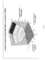
- FIGS. 6 and 7 illustrate PSRO characterization according to methods and systems herein.
- the variable T RO represents the oscillation period of the PSRO
- the variable T 0 represents the mean value of the oscillation period
- the variable ⁇ V represents the deviation of the supply voltage from its nominal value
- the variable a RO,V represents the sensitivity of the oscillation period to the variation of the supply voltage
- the variable ⁇ X Pr represents the deviation of the process variable from its nominal value
- the variable a RO,Pr represents the sensitivity of the oscillation period to the process variation
- the variable ⁇ R represents the variability of the oscillation period due to the other sources of variation like temperature, interconnect metal, across chip variation, uncorrelated random variation, etc.
- the operating voltage (Vdd) decreases as the PSRO period (T) decreases.
- the PSRO period T increases, the process speed increases.
- FIGS. 8 and 9 illustrate the timing results.
- the variable S represents the timing slack of the critical path
- the variable s 0 represents the mean value of the timing slack
- the variable ⁇ V represents the deviation of the supply voltage from its nominal value
- the variable a V represents the sensitivity of the timing slack to the supply voltage variation
- the variable ⁇ X Pr represents the deviation of the process variable from its nominal value
- the variable a Pr represents the sensitivity of the timing slack to the process variation
- the variable ⁇ X T represents the deviation of temperature from its nominal value
- the variable a T represents the sensitivity of the timing slack to the temperature variation
- the variable ⁇ X M represents the variation of the interconnect metal parameters
- the variable a M represents the sensitivity of the timing slack to the variation of the interconnect metal parameters
- the variable ⁇ X R represents the uncorrelated random variability
- the variable a R represents the sensitivity of the timing slack to the uncorrelated random variability
- the variable ⁇ R S represents the combined variation of the timing sl
- the variable T RO represents oscillation period of the PSRO
- the variable T 0 represents mean value of the oscillation period
- the variable ⁇ V represents deviation of supply voltage from its nominal value
- the variable a RO,V represents the sensitivity of the oscillation period to variation of the supply voltage
- the variable ⁇ X Pr represents deviation of process variable from its nominal value
- the variable a RO,Pr represents the sensitivity of the oscillation period to process variation
- the variable ⁇ R represents variability of the oscillating period due to other sources of variation like interconnect metal, across chip variation, uncorrelated random variation, etc.
- the measured PSRO period is T Sens .
- the Vdd of measurement (sensing PSRO) is V Sens .
- the other variability is bounded as ⁇ R Bound ⁇ R ⁇ R Bound , where the variable ⁇ R bound represents the maximum possible variation of the PRSO oscillation period due to the other sources of variation like interconnect metal, across chip variation, etc.
- the variation of the process parameter is estimated as:
- the variable T Sens represents the measured oscillation period of the PSRO
- the variable T 0 represents the mean value of the oscillation period
- the variable ⁇ V Sens represents the deviation of the supply voltage, when the PSRO period is measured, from the nominal value of the supply voltage
- the variable a RO,V represents the sensitivity of the oscillation period to variation of the supply voltage
- the variable ⁇ X Pr represents deviation of the process variable from its nominal value
- the variable a RO,Pr represents the sensitivity of the oscillation period to the process variation
- the variable ⁇ R represents variability of the oscillating period the sources of variation like interconnect metal, across chip variation, uncorrelated random variation, etc.
- the bounded estimate of process parameter assuming a RO,Pr >0 is determined as follows:
- Vdd is computed to ensure Slack>0 (assuming a V >0) is determined as follows:
- the variable ⁇ V represents the deviation of the computed supply voltage from the nominal value, ensuring positive slack
- the variable T Sens represents the measured oscillation period of the PSRO
- the variable T 0 represents the mean value of the oscillation period
- the variable s 0 represents the mean value of the timing slack
- the variable ⁇ V Sens represents the deviation of the supply voltage, when the PSRO period is measured, from the nominal value of the supply voltage
- the variable a RO,V represents the sensitivity of the oscillation period to the variation of the supply voltage
- the variable a V represents the sensitivity of the timing slack to the variation of the supply voltage
- the variable a RO,Pr represents the sensitivity of the oscillation period to the process variation
- the variable a Pr represents the sensitivity of the timing slack to the process variation
- the variable ⁇ R S represents the timing slack variability due to the other sources of variation like interconnect metal, across chip variation, uncorrelated random variation, etc.
- the variable ⁇ R Bound
- T RO T O +a RO,V ⁇ V+a RO,Pr ⁇ X Pr +a RO,t ⁇ X t +a RO,m ⁇ X M + ⁇ R.
- the variable T RO represents the oscillation period of the PSRO
- the variable T 0 represents the mean value of the oscillation period
- the variable ⁇ V represents the deviation of the supply voltage from its nominal value
- the variable a RO,V represents the sensitivity of the oscillation period to the variation of the supply voltage
- the variable ⁇ X Pr represents the deviation of the process variable from its nominal value
- the variable a RO,Pr represents the sensitivity of the oscillation period to the process variation
- the variable ⁇ X t represents the deviation of the temperature from its nominal value
- the variable a t represents the sensitivity of the oscillation period to the temperature
- the variable ⁇ X M represents the deviation of the interconnect metal parameters from their nominal value
- the variable a RO,M represents the sensitivity of the oscillation period to the interconnect metal parameters
- the variable ⁇ R represents variability of the oscillating period due to the other sources of variation like across chip variation, uncorrelated random variation, etc.
- T RO T 0 ( ⁇ V, ⁇ X Pr )+ ⁇ R( ⁇ V, ⁇ X Pr ).
- the variable T RO represents the oscillation period of the PSRO
- the variable T 0 represents the mean value of the oscillation period
- the variable ⁇ V represents the deviation of the supply voltage from its nominal value
- the variable ⁇ X Pr represents the deviation of the process variable from its nominal value
- the term T 0 ( ⁇ V, ⁇ X Pr ) represents the mean value of the oscillation period as a nonlinear function of the supply voltage and the process variations
- the term R( ⁇ V, ⁇ X Pr ) represents the random variation of the oscillation period as nonlinear function of the supply voltage and the process variations.
- Parameters included (and exclude from delta R) are items such as voltage, temperature, and a single Vt.
- the systems and methods herein use all Vt families in a design, to find delta PSRO (systematically calculating across chip variation (ACV)).
- ACV across chip variation
- the methods and systems herein perform statistical analysis of satellite PSROs and consider all metal layer parameters (capacitance, resistance, etc.). Capacitance and resistance are inversely related and are contained in one parameter per layer. These can be taken from kerf data or an on chip monitor.
- the systems and methods herein use the N/P mis-tracking parameter that can be taken from the SPM macro, or possibly from the kerf data.
- T RO T O +a RO,V ⁇ V+a RO,Pr ⁇ X Pr + ⁇ R.
- the systems and methods herein perform a hardware verses modeling comparison of a “PSRO path”.
- Einstimer is used to make a path out of the linear elements in a PSRO.
- a Spice analysis can also be used.
- Hardware comparison is achieved by data gathering and regression.
- the A ROV total is a linear addition of the independent PSRO Vt A ROV s .
- the systems and methods herein provide a plan for back-annotation of all parameters that are not in delta R.
- the systems and methods herein perform the following process at the tester for every chip.
- the systems and methods gather chip specific data, test Voltage, Temp, Kerf Data, SPM Data, PSRO (all PSRO, all Vt).
- the systems and methods herein solve for delta V to create equation inputs and create sigma values to back annotate to path delay equations.
- the systems and methods may shift and scale to annotate the path delay equations.
- the systems and methods mathematically solve for delta V (which gives the bin for each part).
- the systems and methods predict the speed of ASST Paths for chip.
- the systems and methods use sigma values to back annotate into canonicals for the ASST paths and predict the frequency (bound experiment), which is at least not worse than customer speed.
- the systems and methods run ASST at a predicted Vdd and verify passing tests at nominal Vdd minus delta V and determine how this relates to the normal ASST pass/fail criteria. If the chip does not pass, it is either thrown out, or ratcheted down delta V, and the process then tries again. The methods assign binning accordingly.
- T RO,1 T 0,1 +a RO,V,2 ⁇ V+a RO,Vt2 ⁇ X Vt2 + ⁇ R 2 .
- Measured PSRO periods are T Sen1 , T Sen2 .
- Vdd of measurement (sensing PSRO) ⁇ V Sen is the same for all PSROs.
- the other variabilities are bounded as: ⁇ R Bnd1 ⁇ R 1 ⁇ R Bnd2 ⁇ R Bnd2 ⁇ R 2 ⁇ R Bnd2 . Bounds of process parameters for different Vt families (assuming positive sensitivities a RO,Vt >0)
- the variables T R0,1 , T R0,2 represent the oscillation periods of the PSROs of two different Vt families
- the variables T 0,1 , T 0,2 represent the mean values of the PSRO oscillation periods
- the variable ⁇ V represents the deviation of the supply voltage from its nominal value
- the variables a RO,V,1 , a RO,V,1 represent the sensitivities of the oscillation periods to the variation of the supply voltage
- the variables ⁇ X Vt1 , ⁇ X Vt2 represent the deviations of the process variables of two different Vt families from their nominal values
- the variables a RO,Vt1 , a RO,Vt2 represent the sensitivities of the oscillation periods to the process variations of different Vt families
- the variables ⁇ R 1 , ⁇ R 2 represent the variabilities of the oscillating periods due to the other sources of variation like temperature, interconnect metal, across chip variation, uncorrelated random variation, etc.
- the variables ⁇ R Bnd1 , ⁇ R Bnd2 represent
- Bounded timing slack (assuming a Vt1 >0, a Vt2 >0) is determined as follows:
- Vdd computed to ensure that slack is positive (S>0), assuming a V >0 is determined as follows:
- the variable S represents the timing slack of the critical path
- the variable s 0 represents the mean value of the timing slack
- the variable ⁇ V represents the deviation of the supply voltage from its nominal value
- the variable a V represents the sensitivity of the timing slack to the supply voltage variation
- the variables ⁇ X Vt1 , ⁇ X Vt2 represent the deviations of the process variables of two different Vt families from their nominal values
- the variables a Vt1 , a Vt1 represent the sensitivities of the timing slack to the process variations of two different Vt families
- the variable ⁇ R S represents the combined variation of the timing slack due to temperature, interconnect metal and uncorrelated random variability
- the variables T 0,1 , T 0,2 represent the mean values of the PSRO oscillation periods
- the variable ⁇ V represents the deviation of the supply voltage from its nominal value
- the variables a RO,V,1 , a R0,V,1 represent the sensitivities of the oscillation periods to
- every slack value is in canonical form for process and environment parameters. All slack distributions combined give the chip yield value. The slacks are shifted; and all distributions are combined to a new distribution. Also, the smallest slack has the highest weight. The number of paths leading to the slack is also part of this distribution. High and low voltage runs describing the voltage limits are combined. Further, the probability of a zero slack value is the chip yield. The chip yield can be expressed in canonical form as function of the process and environment parameters. The 3 sigma probability which has all slack positive is the chip yield. Additionally, the foregoing depends on all process and environment parameters used in timing.
- the system and methods herein show the values for a set of parameters, including average PSRO values per VT-family—process intrinsic parameter; Delta PSRO for systematic ACV of each chip—process systematic parameter; Ion and Vt for Nfet and Pfet from SPM macro—process N/P off-track parameter; etc.
- the systems and methods herein can also use kerf metal level resistance data—set the metal parameter value.
- the systems and methods herein select a lower voltage for power reduction.
- the systems and methods herein create and store the yield canonical form equation for hardware disposition. This equation can be output from the final timing run.
- the systems and methods herein inset the parameter data for each chip into this yield equation. All non-measured parameters will be held to the WC 3 sigma value, and this will push the yield into the positive range.
- Each non-measured parameter (or a combination of these) can be moved to solve the resulting equation for each specific chip. For example, the Vdd value will give the lowest power with guaranty for a working chip, and the reduction of Vdd will push the yield back to the zero value. Also, the clock frequency change will give the best performance for a working chip. If the chip has selective voltage binning, the systems and methods herein will determine the shipping bin for the specific chip fitting this new reduced Vdd value.
- a canonical form of the ASST path delay values can be used for verification of the method.
- the parameter values measured for the chip can be used to verify the path delay values measured.
- Delay values not dependent on the parameters measured include SRAM delay, PLL delay, VCS sensitivity, Voltage islands need WC timing setting.
- the values can also be verified with the ASST path analysis. Path values can be used to add chip specific values to these items.
- Benefits of the methods and systems herein include higher flexibility and accuracy than the current linear global setting for optimized chip usage.
- ACV is part of the Vdd and bin selection. Currently, ACV stretches over 5 bins. Inclusion of Vt-family data, using the dominant VT group on the chip not the global setting. There is a possibility to include wire results, even for smaller distributions across the wafer from the Kerf data or an on chip monitor. There is an inclusion of N/P parameter setting, and an inclusion of ASST path delay.
- FIGS. 10 and 11 show critical path delay components. Paths are broken up into delay components (shown in different shading in FIGS. 10 and 11 ) that react differently to process voltage and temperature (PVT).
- FIG. 11 is a more generic representation of that shown in FIG. 10 . Items 300 , 302 , 304 , 306 in FIG. 11 show the different path delay mark up components. Thus, critical path predictions that can be made from the PSRO delay samples on the tester are shown in FIGS. 10 and 11 .
- Critical path prediction is the sum of the component parts.
- Path delay is a function of Vdd. The methods and systems herein numerically solve for Vdd as a function of delay with delay set to the cycle time.
- FIG. 12 shows tester SVB method performance recovery resulting from increasing Vdd.
- FIG. 12 shows with Reference Corner (nominal) path timing information.
- the methods predict the path delay.
- prediction is determined that uvt has a 10% increase in delay.
- FIG. 13 shows tester SVB method performance recovery resulting from decreasing Vdd.
- the FIG. 13 shows Reference Corner (CC) path timing information.
- the methods use PSRO delay samples and predict the path delay.
- prediction is determined that uvt has a 20% decrease in delay.
- the methods adjust this performance with voltage for 0 slack (4 ns).
- FIG. 14 is a chart of the path delay Makeup.
- FIG. 14 shows testing using PSRO data, and this determines that all the FET are 10% slow.
- FIG. 14 shows that for each path, the systems and methods herein solve for 0 slack voltage (Vdd).
- Vdd 0 slack voltage
- FIG. 14 shows that the maximum path Vdd required for this chip is +1.083 V.
- FIG. 14 shows that the slow parts are dominated by the least Sensitive Paths (hvt+wire).
- FIG. 14 shows that the fast parts will be dominated by most sensitive paths (uvt only).
- FIG. 15 is a chart of path delay Makeup.
- FIG. 15 shows the corner condition (CC) path timing information.
- CC corner condition
- the methods and systems herein predict that there is a 10% decrease in uvt & hvt delays and a 12% in svt.
- FIG. 15 shows that for each case, the path adjusts this performance with voltage for 0 slack.
- Maximum Path Vdd required for this chip is shown to be 0.939 my.
- FIG. 16 shows a similar chart of path delay showing how the systems and methods herein minimize the number of critical paths to analyze at the test.
- Item 350 shows that the number of paths to evaluate at the tester can be limited to a small number.
- the least sensitive paths dominate. In this case, the path with the most wire dominates.
- FIG. 17 is a chart of path delay Makeup showing how the systems and methods herein minimize the number of critical paths to analyze at the test.
- Item 352 in FIG. 17 shows that with fast parts (giving back voltage), the most sensitive paths dominate. With slow parts (adding voltage to recover performance), the least sensitive paths dominate.
- Item 354 shows that in this case (fast) the path with the most transistor delay dominates. None of the paths in the middle surface as dominating (requiring more voltage).
- the Bounding Path Set can be limited to each VT type with minimum Wire and Maximum Wire which includes: 1) Uvt only, 2) Uvt & max wire, 3) Svt only, 4) Svt & max wire, 5) Hvt only; and 6) Hvt & max wire.
- FIG. 18 is a chart that illustrates delay of logic paths. There are many potential critical paths which become dominant under varying conditions.
- FIG. 19 is a similar chart with HVT delay prediction, and sampled RO delay facts are displayed.
- FIG. 20 is a chart that shows the longest predicted critical path delay as a function of PSRO.
- the samples show uvt ring osc delay factor (from sample) and hvt ring osc delay factor (from sample).
- Critical path prediction is the sum of the component parts.
- ptcp_delay hvt_ptcp_delay+svt_ptcp_delay+uvt_ptcp_delay+wire_ptcp_delay ptcp_delay, Predicted Tester Critical Path Delay, *vt_ptcp_delay, Predicted Tester Critical Path Component Delay dly_hvt_cp_cc, hvt delay of the critical path at a corner condition (Timing Report), dly_hvt_ro_cc, hvt delay of the ring oscillator at a corner condition (Spice Analysis), pcp—Predicted Critical Path, cp—Critical Path.
- FIG. 21 is a chart illustrating the effect of controlling the path occurrence.
- Monte Carlo random simulations are show with max transistor paths and max transistor with max wire paths dominate.
- Methods and systems herein perform delay prediction using parametric wire delay information and wire information from a wire PSRO that includes selectable wire delay paths.
- the methods can utilize the power of an EinsTimer to identify critical path information and sensitivities and can perform extraction of Canonical Equations (Parameter Sensitivities).
- FIG. 22 is a flow diagram illustrating an exemplary a method of optimizing power usage in an integrated circuit design.
- this method manufactures integrated circuit devices according to the same integrated circuit design, using manufacturing equipment.
- the integrated circuit design produces integrated circuit devices that are identically designed and are produced in what is intended to be the same manufacturing process, yet some perform at different operating speeds because of unintended or physically uncontrollable manufacturing process variations.
- this method determines the operating speed of each of the integrated circuit devices based on delay parameters that are applied to a canonical equation that evaluates the different threshold voltage portions of each of the integrated circuit devices differently.
- the canonical equation in item 402 can be customized for each of the integrated circuit devices based on ranges of the delay parameters.
- the method can determine the operating speed of each of the integrated circuit devices by obtaining data from at least one ring oscillator positioned within each of the different threshold voltage portions.
- the determination of the operating speed of each of the integrated circuit devices 402 includes determining across chip variations (ACV) of the delay parameters.
- the determination of the operating speed of each of the integrated circuit devices 402 can be made: by examination of theoretical control paths (TCP); using a yield equation to find voltages that produce zero timing slack within each of the integrated circuit devices; using multiple controlling canonical slack equations that weigh performance against voltage to produce non-linear delay measures, etc.
- This method also sorts the integrated circuit devices after manufacture into relatively slow integrated circuit devices and relatively fast integrated circuit devices based on the operating speed of each of the integrated circuit devices to classify the integrated circuit devices into different voltage bins in item 404 .
- the relatively fast integrated circuit devices consume more power than the relatively slow integrated circuit devices and, therefore, operating voltages of the integrated circuit devices can be altered according to the voltage bins to optimize power usage.
- this method can embed voltage bin information in each of the integrated circuit devices based on which of the different voltage bins each of the integrated circuit devices has been classified in item 406 .
- the voltage bin information can be used to control the operating voltage at which each of the integrated circuit devices are to be operated.
- FIG. 23 illustrates an additional embodiment herein which is a device (support) 440 that comprises a plurality of digital circuits 450 manufactured from an identical circuit design, a power controller or tester 460 operatively connect to the digital circuits, and a non-transitory storage medium 452 operatively connected to the power controller/tester 460 .
- all the digital circuits 450 are application specific integrated circuits (ASIC); however, as would be understood by those ordinarily skilled in the art, any device could be used with the embodiments herein.
- the digital circuits 450 are classified into different voltage bins. Each of the digital circuits 450 is tested to operate within a corresponding current leakage limit of a corresponding voltage bin into which each of the digital circuits has been classified.
- the non-transitory storage medium 452 stores boundaries of the voltage bins as speed-binning test data.
- the speed-binning test data has been generated and stored in the non-transitory storage medium 452 during production testing of the digital circuits.
- the non-transitory storage medium 452 can comprise, for example, a programmable fuse block.
- the power controller/tester 460 determines a speed constraint for a task to be executed by a given digital circuit 450 based on a voltage bin to which the digital circuit has been classified, and the power controller/tester 460 also specifies levels of the power-supply signals for execution of the task based on such a speed constraint.
- Some embodiments can also include a sensor 454 that senses the temperature of a given digital circuit.
- Additional embodiments can also include a power management unit (PMU) 470 that receives instructions from the power controller/tester 460 regarding levels of the power-supply signals and generates the power-supply signals based on the instructions.
- PMU power management unit
- test device 460 can be operatively (directly or indirectly) connected to the integrated circuit devices through the support 440 .
- a non-transitory storage medium 452 can be operatively connected to the test device. The test device performs testing according to instructions stored in the non-transitory storage medium.
- the instructions causing the test device to perform a method that determines an operating speed of each of the integrated circuit devices based on delay parameters applied to a canonical equation that evaluates different threshold voltage portions of each of the integrated circuit devices differently. Again, each of the different threshold voltage portions of the integrated circuit devices operating at different threshold voltages.
- the instructions further cause the test device to sort the integrated circuit devices after manufacture into relatively slow integrated circuit devices and relatively fast integrated circuit devices based on the operating speed of each of the integrated circuit devices, to classify the integrated circuit devices into different voltage bins.
- the relatively fast integrated circuit devices again consume more power than the relatively slow integrated circuit devices.
- the instructions also cause the test device to embed voltage bin information in the integrated circuit devices based on which of the different voltage bins each of the integrated circuit devices has been classified. The voltage bin information controls the operating voltage at which each of the integrated circuit devices are to be operated.
- FIG. 24 A representative hardware environment for practicing the embodiments herein is depicted in FIG. 24 .
- the system comprises at least one processor or central processing unit (CPU) 10 .
- the CPUs 10 are interconnected via system bus 12 to various devices such as a random access memory (RAM) 14 , read-only memory (ROM) 16 , and an input/output (I/O) adapter 18 .
- RAM random access memory
- ROM read-only memory
- I/O input/output
- the I/O adapter 18 can connect to peripheral devices, such as disk units 11 and tape drives 13 , or other program storage devices that are readable by the system.
- the system can read the inventive instructions on the program storage devices and follow these instructions to execute the methodology of the embodiments herein.
- the system further includes a user interface adapter 19 that connects a keyboard 15 , mouse 17 , speaker 24 , microphone 22 , and/or other user interface devices such as a touch screen device (not shown) to the bus 12 to gather user input.
- a communication adapter 20 connects the bus 12 to a data processing network 25
- a display adapter 21 connects the bus 12 to a display device 23 which may be embodied as an output device such as a monitor, printer, or transmitter, for example.
- each block in the flowchart or block diagrams may represent a module, segment, or portion of code, which comprises one or more executable instructions for implementing the specified logical function(s).
- the functions noted in the block may occur out of the order noted in the figures. For example, two blocks shown in succession may, in fact, be executed substantially concurrently, or the blocks may sometimes be executed in the reverse order, depending upon the functionality involved.
Abstract
Description
T RO =T 0 +a RO,V ΔV+a RO,Pr ΔX Pr +ΔR
S=s 0 +a V ΔV+a Pr ΔX Pr +a T ΔX T +a M ΔX M +a R ΔX R =s 0 +a V ΔV+a Pr ΔX Pr +ΔR S.
T RO =T O +a RO,V ΔV+a RO,Pr ΔX Pr +a RO,t ΔX t +a RO,m ΔX M +ΔR.
T RO,1 =T 0,1 +a RO,V,1 ΔV+a RO,Vt1 ΔX Vt1 +ΔR 1
T RO,1 =T 0,1 +a RO,V,2 ΔV+a RO,Vt2 ΔX Vt2 +ΔR 2.
-
-
Coefficient 3 corresponds to 3 sigma estimate
-
Claims (24)
Priority Applications (1)
| Application Number | Priority Date | Filing Date | Title |
|---|---|---|---|
| US13/614,564 US9157956B2 (en) | 2012-09-13 | 2012-09-13 | Adaptive power control using timing canonicals |
Applications Claiming Priority (1)
| Application Number | Priority Date | Filing Date | Title |
|---|---|---|---|
| US13/614,564 US9157956B2 (en) | 2012-09-13 | 2012-09-13 | Adaptive power control using timing canonicals |
Publications (2)
| Publication Number | Publication Date |
|---|---|
| US20140074422A1 US20140074422A1 (en) | 2014-03-13 |
| US9157956B2 true US9157956B2 (en) | 2015-10-13 |
Family
ID=50234175
Family Applications (1)
| Application Number | Title | Priority Date | Filing Date |
|---|---|---|---|
| US13/614,564 Active 2034-05-29 US9157956B2 (en) | 2012-09-13 | 2012-09-13 | Adaptive power control using timing canonicals |
Country Status (1)
| Country | Link |
|---|---|
| US (1) | US9157956B2 (en) |
Cited By (2)
| Publication number | Priority date | Publication date | Assignee | Title |
|---|---|---|---|---|
| US20140316731A1 (en) * | 2013-04-23 | 2014-10-23 | Apple Inc. | Continuous voltage product binning |
| US9430603B1 (en) | 2015-12-04 | 2016-08-30 | International Business Machines Corporation | Scaling voltages in relation to die location |
Families Citing this family (2)
| Publication number | Priority date | Publication date | Assignee | Title |
|---|---|---|---|---|
| US9865486B2 (en) | 2016-03-29 | 2018-01-09 | Globalfoundries Inc. | Timing/power risk optimized selective voltage binning using non-linear voltage slope |
| US10840157B2 (en) * | 2017-06-02 | 2020-11-17 | University of Viriginia Patent Foundation | Methods for reducing chip testing time using trans-threshold correlations |
Citations (9)
| Publication number | Priority date | Publication date | Assignee | Title |
|---|---|---|---|---|
| US20070016833A1 (en) | 2005-07-18 | 2007-01-18 | Chih-Wen Lin | Method For Performing Built-In And At-Speed Test In System-On-Chip |
| US7174523B2 (en) | 2004-07-30 | 2007-02-06 | International Business Machines Corporation | Variable sigma adjust methodology for static timing |
| US7240304B2 (en) | 2004-05-04 | 2007-07-03 | Freescale Semiconductor, Inc. | Method for voltage drop analysis in integreted circuits |
| US20080034337A1 (en) | 2006-08-04 | 2008-02-07 | Kuemerle Mark W | integrated circuit design closure method for selective voltage binning |
| WO2008134215A1 (en) | 2007-04-27 | 2008-11-06 | International Business Machines Corporation | Ic chip at-functional-speed testing with process coverage evaluation |
| US20090115468A1 (en) | 2005-10-14 | 2009-05-07 | Infineon Technologies Ag | Integrated Circuit and Method for Operating an Integrated Circuit |
| US20090228843A1 (en) | 2008-03-04 | 2009-09-10 | International Business Machines Corporation | Method to optimize power by tuning the selective voltage binning cut point |
| US20110181337A1 (en) | 2010-01-25 | 2011-07-28 | Renesas Electronics Corporation | Semiconductor integrated circuit and electronic device |
| US8543960B1 (en) * | 2012-05-31 | 2013-09-24 | International Business Machines Corporation | Power and timing optimization for an integrated circuit by voltage modification across various ranges of temperatures |
-
2012
- 2012-09-13 US US13/614,564 patent/US9157956B2/en active Active
Patent Citations (11)
| Publication number | Priority date | Publication date | Assignee | Title |
|---|---|---|---|---|
| US7240304B2 (en) | 2004-05-04 | 2007-07-03 | Freescale Semiconductor, Inc. | Method for voltage drop analysis in integreted circuits |
| US7174523B2 (en) | 2004-07-30 | 2007-02-06 | International Business Machines Corporation | Variable sigma adjust methodology for static timing |
| US20070016833A1 (en) | 2005-07-18 | 2007-01-18 | Chih-Wen Lin | Method For Performing Built-In And At-Speed Test In System-On-Chip |
| US20090115468A1 (en) | 2005-10-14 | 2009-05-07 | Infineon Technologies Ag | Integrated Circuit and Method for Operating an Integrated Circuit |
| US20080034337A1 (en) | 2006-08-04 | 2008-02-07 | Kuemerle Mark W | integrated circuit design closure method for selective voltage binning |
| US7475366B2 (en) | 2006-08-04 | 2009-01-06 | International Business Machines Corporation | Integrated circuit design closure method for selective voltage binning |
| WO2008134215A1 (en) | 2007-04-27 | 2008-11-06 | International Business Machines Corporation | Ic chip at-functional-speed testing with process coverage evaluation |
| US7620921B2 (en) | 2007-04-27 | 2009-11-17 | International Business Machines Corporation | IC chip at-functional-speed testing with process coverage evaluation |
| US20090228843A1 (en) | 2008-03-04 | 2009-09-10 | International Business Machines Corporation | Method to optimize power by tuning the selective voltage binning cut point |
| US20110181337A1 (en) | 2010-01-25 | 2011-07-28 | Renesas Electronics Corporation | Semiconductor integrated circuit and electronic device |
| US8543960B1 (en) * | 2012-05-31 | 2013-09-24 | International Business Machines Corporation | Power and timing optimization for an integrated circuit by voltage modification across various ranges of temperatures |
Cited By (4)
| Publication number | Priority date | Publication date | Assignee | Title |
|---|---|---|---|---|
| US20140316731A1 (en) * | 2013-04-23 | 2014-10-23 | Apple Inc. | Continuous voltage product binning |
| US9368416B2 (en) * | 2013-04-23 | 2016-06-14 | Apple Inc. | Continuous voltage product binning |
| US9430603B1 (en) | 2015-12-04 | 2016-08-30 | International Business Machines Corporation | Scaling voltages in relation to die location |
| US9594868B1 (en) | 2015-12-04 | 2017-03-14 | International Business Machines Corporation | Scaling voltages in relation to die location |
Also Published As
| Publication number | Publication date |
|---|---|
| US20140074422A1 (en) | 2014-03-13 |
Similar Documents
| Publication | Publication Date | Title |
|---|---|---|
| US9536038B1 (en) | Method and algorithm for functional critical paths selection and critical path sensors and controller insertion | |
| US7475366B2 (en) | Integrated circuit design closure method for selective voltage binning | |
| US8421495B1 (en) | Speed binning for dynamic and adaptive power control | |
| US5751593A (en) | Accurate delay prediction based on multi-model analysis | |
| US8020130B2 (en) | Timing analysis apparatus and method for semiconductor integrated circuit in consideration of power supply and ground noises | |
| US7472038B2 (en) | Method of predicting microprocessor lifetime reliability using architecture-level structure-aware techniques | |
| Wirnshofer | Variation-aware adaptive voltage scaling for digital CMOS circuits | |
| US7992114B1 (en) | Timing analysis using statistical on-chip variation | |
| US8762087B2 (en) | Accurate integrated circuit performance prediction using on-board sensors | |
| US7299438B2 (en) | Method and apparatus for verifying semiconductor integrated circuits | |
| US11475187B2 (en) | Augmented reliability models for design and manufacturing | |
| US5787008A (en) | Simulation corrected sensitivity | |
| US20040002844A1 (en) | System and method for statistical modeling and statistical timing analysis of integrated circuits | |
| US5790415A (en) | Complementary network reduction for load modeling | |
| US20080209373A1 (en) | Method and system for evaluating statistical sensitivity credit in path-based hybrid multi-corner static timing analysis | |
| US9557378B2 (en) | Method and structure for multi-core chip product test and selective voltage binning disposition | |
| US9157956B2 (en) | Adaptive power control using timing canonicals | |
| TWI451281B (en) | Characterising circuit cell performance variability in response to perturbations in manufacturing process parameters | |
| US10474774B2 (en) | Power and performance sorting of microprocessors from first interconnect layer to wafer final test | |
| US9892220B2 (en) | Method and apparatus for adjusting a timing derate for static timing analysis | |
| US7756653B2 (en) | Storage medium storing thereon power consumption analysis program, and power consumption analysis method | |
| Sadi et al. | SoC speed binning using machine learning and on-chip slack sensors | |
| US8448110B2 (en) | Method to reduce delay variation by sensitivity cancellation | |
| US7861130B2 (en) | System and method of determining the speed of digital application specific integrated circuits | |
| JP5567322B2 (en) | Test flow presentation computer program, test flow presentation computer system |
Legal Events
| Date | Code | Title | Description |
|---|---|---|---|
| AS | Assignment |
Owner name: INTERNATIONAL BUSINESS MACHINES CORPORATION, NEW Y Free format text: ASSIGNMENT OF ASSIGNORS INTEREST;ASSIGNORS:BICKFORD, JEANNE P.;FOREMAN, ERIC A.;HABITZ, PETER A.;AND OTHERS;SIGNING DATES FROM 20120807 TO 20120821;REEL/FRAME:028957/0027 |
|
| FEPP | Fee payment procedure |
Free format text: PAYOR NUMBER ASSIGNED (ORIGINAL EVENT CODE: ASPN); ENTITY STATUS OF PATENT OWNER: LARGE ENTITY Free format text: PAYER NUMBER DE-ASSIGNED (ORIGINAL EVENT CODE: RMPN); ENTITY STATUS OF PATENT OWNER: LARGE ENTITY |
|
| AS | Assignment |
Owner name: GLOBALFOUNDRIES U.S. 2 LLC, NEW YORK Free format text: ASSIGNMENT OF ASSIGNORS INTEREST;ASSIGNOR:INTERNATIONAL BUSINESS MACHINES CORPORATION;REEL/FRAME:036550/0001 Effective date: 20150629 |
|
| STCF | Information on status: patent grant |
Free format text: PATENTED CASE |
|
| AS | Assignment |
Owner name: GLOBALFOUNDRIES INC., CAYMAN ISLANDS Free format text: ASSIGNMENT OF ASSIGNORS INTEREST;ASSIGNORS:GLOBALFOUNDRIES U.S. 2 LLC;GLOBALFOUNDRIES U.S. INC.;REEL/FRAME:036779/0001 Effective date: 20150910 |
|
| AS | Assignment |
Owner name: WILMINGTON TRUST, NATIONAL ASSOCIATION, DELAWARE Free format text: SECURITY AGREEMENT;ASSIGNOR:GLOBALFOUNDRIES INC.;REEL/FRAME:049490/0001 Effective date: 20181127 |
|
| FEPP | Fee payment procedure |
Free format text: MAINTENANCE FEE REMINDER MAILED (ORIGINAL EVENT CODE: REM.); ENTITY STATUS OF PATENT OWNER: LARGE ENTITY |
|
| FEPP | Fee payment procedure |
Free format text: SURCHARGE FOR LATE PAYMENT, LARGE ENTITY (ORIGINAL EVENT CODE: M1554); ENTITY STATUS OF PATENT OWNER: LARGE ENTITY |
|
| MAFP | Maintenance fee payment |
Free format text: PAYMENT OF MAINTENANCE FEE, 4TH YEAR, LARGE ENTITY (ORIGINAL EVENT CODE: M1551); ENTITY STATUS OF PATENT OWNER: LARGE ENTITY Year of fee payment: 4 |
|
| AS | Assignment |
Owner name: GLOBALFOUNDRIES U.S. INC., CALIFORNIA Free format text: ASSIGNMENT OF ASSIGNORS INTEREST;ASSIGNOR:GLOBALFOUNDRIES INC.;REEL/FRAME:050122/0001 Effective date: 20190821 |
|
| AS | Assignment |
Owner name: MARVELL INTERNATIONAL LTD., BERMUDA Free format text: ASSIGNMENT OF ASSIGNORS INTEREST;ASSIGNOR:GLOBALFOUNDRIES U.S. INC.;REEL/FRAME:051070/0625 Effective date: 20191105 |
|
| AS | Assignment |
Owner name: CAVIUM INTERNATIONAL, CAYMAN ISLANDS Free format text: ASSIGNMENT OF ASSIGNORS INTEREST;ASSIGNOR:MARVELL INTERNATIONAL LTD.;REEL/FRAME:052918/0001 Effective date: 20191231 |
|
| AS | Assignment |
Owner name: MARVELL ASIA PTE, LTD., SINGAPORE Free format text: ASSIGNMENT OF ASSIGNORS INTEREST;ASSIGNOR:CAVIUM INTERNATIONAL;REEL/FRAME:053475/0001 Effective date: 20191231 |
|
| AS | Assignment |
Owner name: GLOBALFOUNDRIES INC., CAYMAN ISLANDS Free format text: RELEASE BY SECURED PARTY;ASSIGNOR:WILMINGTON TRUST, NATIONAL ASSOCIATION;REEL/FRAME:054636/0001 Effective date: 20201117 |
|
| MAFP | Maintenance fee payment |
Free format text: PAYMENT OF MAINTENANCE FEE, 8TH YEAR, LARGE ENTITY (ORIGINAL EVENT CODE: M1552); ENTITY STATUS OF PATENT OWNER: LARGE ENTITY Year of fee payment: 8 |