US7756653B2 - Storage medium storing thereon power consumption analysis program, and power consumption analysis method - Google Patents
Storage medium storing thereon power consumption analysis program, and power consumption analysis method Download PDFInfo
- Publication number
- US7756653B2 US7756653B2 US12/054,158 US5415808A US7756653B2 US 7756653 B2 US7756653 B2 US 7756653B2 US 5415808 A US5415808 A US 5415808A US 7756653 B2 US7756653 B2 US 7756653B2
- Authority
- US
- United States
- Prior art keywords
- data set
- circuit data
- power consumption
- wirelines
- toggle
- Prior art date
- Legal status (The legal status is an assumption and is not a legal conclusion. Google has not performed a legal analysis and makes no representation as to the accuracy of the status listed.)
- Expired - Fee Related, expires
Links
Images


Classifications
-
- G—PHYSICS
- G06—COMPUTING; CALCULATING OR COUNTING
- G06F—ELECTRIC DIGITAL DATA PROCESSING
- G06F30/00—Computer-aided design [CAD]
- G06F30/30—Circuit design
- G06F30/36—Circuit design at the analogue level
- G06F30/367—Design verification, e.g. using simulation, simulation program with integrated circuit emphasis [SPICE], direct methods or relaxation methods
-
- G—PHYSICS
- G06—COMPUTING; CALCULATING OR COUNTING
- G06F—ELECTRIC DIGITAL DATA PROCESSING
- G06F2119/00—Details relating to the type or aim of the analysis or the optimisation
- G06F2119/06—Power analysis or power optimisation
Definitions
- the present invention relates to a computer-readable storage medium (simply “storage medium”, herebelow) storing thereon a power consumption analysis program, and a power consumption analysis method. More specifically, the invention relates to a power consumption analysis program and method for computing the amount of power consumption of a semiconductor circuit in accordance with load capacities and toggle rates of wirelines of the semiconductor circuit.
- wirelines and the like are reconsidered and modified many times until completion of the design.
- a designer has to calculate the power consumption of the modified semiconductor circuit in accordance with wireline load capacities and toggle rates of the circuitry, thereby to determine whether the result satisfies required conditions.
- the wireline load capacity can be relatively easily calculated when a process-targeted semiconductor circuit is determined.
- the respective toggle rates have to be calculated by simulating the operation of the modified semiconductor circuit. Consequently, there arises a problem that it potentially takes time and cost for the calculation of the toggle rates.
- the scale of the semiconductor circuit such as an LSI
- the number of wirelines therein is larger.
- time and cost for the calculation of the wireline toggle rates are very large.
- TAT turn-around time
- the time (TAT: turn-around time) of the analysis process for the amount of power consumption is increased, potentially leading to a delay in design.
- a designer takes a countermeasure in such a manner that the analysis process of the amount of power consumption is not actually performed in each time of reconsideration/modification, but an appropriate amount of power consumption is estimated. Thereby the analysis process for the amount of power consumption is performed only with respect to essential points of reconsideration/modification of wireline and the like.
- a storage medium storing thereon a power consumption analysis program operable to cause a computer to function as a power consumption analysis apparatus.
- the apparatus includes a device for preliminarily providing a first toggle rate of each of a plurality of wirelines included in a first circuit data set; a device for generating a correlation in accordance with each first toggle rate and each load capacity of the corresponding wireline, each correlation being indicative of a relationship between the first toggle rate and the load capacity; and a device for calculating a second toggle rate of each of a plurality of wirelines included in a second circuit data set, in accordance with a load capacity of a corresponding wireline and the corresponding correlation.
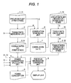
- FIG. 1 is a diagram showing an example of the configuration of a power consumption analysis apparatus
- FIG. 2 is a flow chart showing the design process of a semiconductor circuit
- FIGS. 3A and 3B are flow charts of examples of power consumption analysis processes
- FIGS. 4A and 4B are explanatory diagrams of the examples of power consumption analysis processes shown in FIGS. 3A and 3B ;
- FIGS. 5A and 5B are explanatory diagrams of the examples of power consumption analysis processes shown in FIGS. 3A and 3B ;
- FIG. 6 is a flow chart related to the examples of the respective power consumption analysis processes
- FIGS. 7A to 7C are explanatory diagrams of the power consumption analysis process
- FIG. 8 is an explanatory diagram of the example of the power consumption analysis process
- FIG. 9 is a flow chart of an example of a power consumption analysis process
- FIG. 10 is a flow chart of another example of the power consumption analysis process.
- FIG. 11 is a flow chart of the power consumption analysis process
- FIGS. 12A to 12C are explanatory diagrams of an example of the power consumption analysis process shown in FIG. 9 ;
- FIGS. 13A and 13B are explanatory diagrams of another example of the power consumption analysis process shown in FIG. 9 ;
- FIG. 14 is a flow chart of still another example of the power consumption analysis process
- FIGS. 15A to 15C are explanatory diagrams of the example of the power consumption analysis process shown in FIG. 14 ;
- FIG. 16 is a diagram showing an example of the configuration of a conventional power consumption analysis apparatus.
- FIG. 1 is a diagram showing an example of the configuration of a power consumption analysis apparatus.
- the power consumption analysis apparatus includes an toggle rate measuring unit 2 , a power consumption calculating unit 4 , a correlation generating unit 6 , a previous information comparing unit 8 , a display unit 9 , and an toggle rate calculating unit 10 .
- the power consumption calculating unit 4 is, for example, implemented in the manner that a power consumption analysis program existing in a main memory is executed on a central processing unit (CPU).
- CPU central processing unit
- the toggle rate measuring unit 2 , the correlation generating unit 6 , the previous information comparing unit 8 , and the toggle rate calculating unit 10 are similarly implemented.
- Circuit data sets 1 are preliminarily prepared (preliminarily generated) by a tool, such as a designing apparatus (not shown), and are respectively input into the power consumption analysis apparatus. More specifically, the circuit data sets 11 and 12 , respectively, are stored in circuit storage units or memories ( 11 and 12 ). Toggle rates 3 ( 31 and 32 ) and power consumption 5 are calculated by the power consumption analysis apparatus. Alternatively, the toggle rates 3 ( 31 and 32 ) may each be represented by ⁇ , herebelow.
- the circuit data set 11 is a circuit data set (first or first version circuit data set) of a semiconductor circuit (LSI) that is obtained from first stage circuit design.
- the circuit data set 12 is a circuit data set (second or subsequent version circuit data set) of the semiconductor circuit that is obtained from second or subsequent stage circuit design.
- the toggle rate 31 is an toggle rate (first stage toggle rate) corresponding to the first stage circuit data set 11 .
- the toggle rate 32 is an toggle rate (second or subsequent toggle rate) corresponding to the second or subsequent stage circuit data set 12 .
- the second or subsequent stage circuit design process does not have to be a design process of the entirety of the semiconductor circuit, but may be a design process of a partial modification of the semiconductor circuit.
- the design process of the semiconductor circuit is carried out along a flow such as described in FIG. 2 .
- a first stage circuit data set 11 can be obtained.
- first stage circuit verification (circuit verification # 1 ) is performed for the first stage circuit data set 11 .
- a first power consumption analysis (power consumption analysis # 1 ) is executed by the power consumption analysis apparatus.
- the series of the processes described above is executed as a first series process, and the first series process is iterated n times. More specifically, the circuit verification is executed in each circuit design process, and the power consumption analysis is executed in the course of the design process. As such, for the second or subsequent stage circuit data set 12 , circuit verifications # 2 to #n, and power consumption analyses # 2 to #n are executed in the course of the circuit verifications # 2 to #n.
- the toggle rate measuring unit 2 is a device that measures respective first stage toggle rates 31 in accordance with the first stage circuit data set 11 in response to a command input operation (performed by a user) for initiation of execution of, for example, a simulation program S described further below.
- the respective first stage toggle rate 31 is calculated by a known (conventional) process, and is stored in an toggle rate storage unit or memory ( 31 ). More specifically, the first stage toggle rate 31 is calculated in the manner that operation of the semiconductor circuit is simulated by simulator (not shown) with the use of the first stage circuit data 11 . As such, time and cost are necessary for the toggle rate calculation.
- the configuration may be such that the first stage toggle rate 31 is prepared (preliminarily generated) and input into the power consumption analysis apparatus.
- the simulation program S is loaded into the toggle rate measuring unit 2 and is executed therein to calculate the first stage toggle rate 31 . In this manner, the first stage toggle rate 31 is calculated.
- the toggle rate (%) is the probability of a transition of a signal value from a high/low to low/high level in one clock cycle in a wireline. It is assumed herein that the toggle rate is 100% when the probability is similar as in the clock (i.e., when two transitions occur per one clock cycle).
- the toggle rate calculating unit 10 is a device that, in accordance with the second or subsequent stage circuit data set 12 , calculates a respective toggle rate 32 (second or subsequent stage toggle rate) corresponding to the circuit data set 12 in response to, for example, the command input operation for execution initiation.
- a respective correlation 7 is used for the calculation. More specifically, in accordance with the second or subsequent stage circuit data set 12 and correlation 7 , the toggle rate calculating unit 10 calculates the respective second or subsequent stage toggle rate 32 and stores it into an toggle rate storage unit or memory ( 32 ).
- the first stage first stage toggle rate 31 is calculated by the known process
- the second or subsequent stage toggle rate 32 is calculated in accordance with the inventive manner, thereby to differentiate the toggle rates 31 and 32 from each other.
- the correlation generating unit 6 is a device that, in response to a notification of completion of calculation of the first stage toggle rate 31 , generates the correlation 7 in accordance with the first stage circuit data set 11 and toggle rate 31 .
- the correlation generating unit 6 stores the generated correlation 7 into a correlation storage unit or memory ( 7 ).
- the correlation 7 is generated prior to calculation of the second or subsequent stage toggle rate 32 .
- the correlation 7 is information indicative of the correlation between a load capacity C and toggle rate ⁇ of a respective wireline.
- the correlation 7 will be represented as “r” or “r( ⁇ , C)”, herebelow. As described below in more detail, the correlation 7 is different corresponding to a calculation process therefor.
- the wireline load capacity C in the first stage circuit data set 11 is calculated by a load capacity calculating unit (not shown) before calculation of the first stage first stage toggle rate 31 .
- the load capacity C can be relatively easily calculated when the circuit data set is determined.
- the configuration may be such that the respective first stage circuit data set 11 includes the load capacity C preliminarily calculated by the designing apparatus (not shown).
- a similar arrangement may be made for the wireline load capacity C in the second or subsequent stage circuit data set 12 .
- the power consumption calculating unit 4 is a device that calculates the respective power consumption 5 by use of the toggle rates 3 ( 31 and 32 ) in response to, for example, a command input operation for initiation of execution. Then the power consumption calculating unit 4 either stores the power consumption 5 into a power consumption storage unit or memory ( 5 ) or prints out the power consumption 5 from a printer (not shown). Alternatively, the power consumption 5 may be represented by P, hereinbelow.
- Pd denotes a power consumption in a dynamic mode of the semiconductor circuit (the amount of power consumed in the semiconductor circuit during operation), and dynamically variable
- Ps denotes a power consumption in a static mode of the semiconductor circuit (the amount of power consumed in the semiconductor circuit even during non-operation), and takes substantially a constant value (since Ps is thus constant, calculation thereof can be omitted).
- V denotes an operating voltage
- f denotes an operating frequency
- Ileak denotes a leaking current.
- the operating voltage V, the operating frequency f, and the leaking current are input into the power consumption calculating unit 4 .
- the leaking current Ileak is mainly a leaking current in a PN junction, so that when the circuit data set is determined, the leaking current Ileak can be easily calculated in accordance with the data set.
- the configuration may be such that the leaking current Ileak is calculated by the power consumption calculating unit 4 .
- the circuit data sets 11 and 12 also are input into the power consumption calculating unit 4 . In this case, the load capacity C is similarly input into the power consumption calculating unit 4 .
- the load capacity C is mainly a wireline capacity and junction capacity, so that when the circuit data set is determined, the load capacity C can be easily calculated in accordance with the load capacity C and the correlation r.
- the toggle rate ⁇ is calculated using the load capacity C and the correlation r in accordance with a predetermined manner of the present embodiment.
- the range (section) of one wireline is determined in accordance with the circuit data set.
- circuit elements such as an AND gate and inverter
- the leaking current and load capacity C of the wireline are calculated.
- the leaking current and load capacity C of one wireline include the leaking current and load capacity C of the circuit element connected to the wireline.
- the previous information comparing unit 8 is a device that performs comparison between a power consumption calculated from a latest circuit data set and an immediately previous stage circuit data set to the latest circuit data set in response a notification of the power consumption, which corresponds to the latest circuit data set, from the power consumption calculating unit 4 . More specifically, it is herein assumed that the latest circuit data set is an i-th stage circuit data set ( 12 ). In this case, the previous information comparing unit 8 performs comparison between a power consumption P(i ⁇ 1) calculated regarding an (i ⁇ 1)th circuit data set and a respective power consumption Pi calculated for the i-th circuit data set.
- the power consumption Pi is input into the previous information comparing unit 8 from the power consumption calculating unit 4 .
- the power consumption P(i ⁇ 1) is obtained by the previous information comparing unit 8 from the power consumption storage unit storing the power consumption 5 .
- the previous information comparing unit 8 calculates a differential therebetween and notifies the display unit 9 of the result for display thereon.
- the display unit 9 operates such that a circuit diagram of the semiconductor circuit is generated in accordance with the circuit data sets 11 and 12 , a wireline having a largest differential in the circuit diagram corresponding to the i-th time (latest) circuit data set is highlight-displayed on the display unit 9 .
- circuit data sets 11 and 12 are input into the display unit 9 .
- the (i ⁇ 1)th stage circuit data set is changed to the i-th time, whereby the user is enabled to easily know the wireline having the largest variation in power consumption.
- FIGS. 3A and 3B are flow charts of examples of power consumption analysis processes. More specifically, FIG. 3A is a flow chart of an exemplary power consumption analysis process for the first stage circuit data set 11 , and FIG. 3B is a flow chart of an exemplary power consumption analysis process for the second or subsequent stage circuit data set 12 .
- FIGS. 4A and 4B and FIGS. 5A and 5B are explanatory diagrams of the example power consumption analysis processes shown in FIGS. 3A and 3B .
- toggle rates ⁇ (first toggle rates) of respective wirelines of the first stage circuit data set 11 are calculated in the manner that the first stage circuit data set 11 is simulated with the simulator (in the simulation manner or conventional manner).
- a table t ( FIG. 4B ) of load capacities C and the first toggle rates ⁇ , and respective correlations r are generated in accordance with the table t.
- toggle rates ⁇ are calculated in accordance with the respective correlations r and the load capacities C of the respective wirelines.
- load capacities C ( FIG. 4A ) of the respective wirelines are calculated by the load capacity calculating unit (not shown) (at step S 11 ).
- the toggle rates ⁇ of the respective wirelines are calculated by the toggle rate measuring unit 2 in the simulation manner in accordance with the first stage circuit data set 11 (at step S 11 ).
- the table t of the load capacities C and toggle rates ⁇ of the respective wirelines are generated by the correlation generating unit 6 , and respective correlations r are generated thereby in accordance with the table t (at step S 12 ).
- power consumptions P are calculated by the power consumption calculating unit 4 in accordance with the load capacities C and toggle rates ⁇ of the respective wirelines (at step S 13 ).
- first stage circuit data set 11 As an example, it is assumed that, as shown in FIG. 4A , as a result of completion of first stage circuit design, a semiconductor circuit including nine wirelines A to I is present (hence, first stage circuit data set 11 is present).
- load capacities C of the wirelines A to I are calculated. The calculation is performed in the conventional manner.
- the calculated load capacities C are shown in FIG. 4A .
- the load capacities C are stored together with the first stage circuit data set 11 . In other words, the load capacities C may be considered to configure part of the circuit data set (this applies also in description below).
- toggle rates ⁇ thereof are calculated.
- the calculated toggle rates ⁇ are shown in FIG. 4B (which shows the table t). More specifically, in FIG. 3A , while the generation of the table t is not shown as one step, the table t is generated in practice in a similar manner as at step S 42 in FIG. 9 described below.
- correlations r between the respective load capacities C and toggle rates ⁇ of the wirelines A to I are generated.
- design of the semiconductor circuit, which includes the wirelines A to I is changed. More specifically, as a result of completion of the second or subsequent stage circuit design, the second or subsequent stage circuit data set 12 , as shown in FIG. 5A , of the semiconductor circuit, which includes the wirelines A to I, can be obtained.
- load capacities C of the wirelines A to I are calculated in accordance with the conventional manner.
- the load capacities C thus calculated are shown in FIG. 5A .
- the load capacity C thereof is varied to from 140 in FIG. 4A to 144 in FIG. 5A .
- similar variations occur.
- the toggle rate calculating unit 10 operates as follows.
- a wireline data item of one wireline n is retrieved from the second or subsequent stage circuit data set 12 (at step S 21 ).
- an toggle rate ⁇ thereof is calculated in accordance with a corresponding load capacity C and correlation r (at step S 22 ).
- the toggle rate calculating unit 10 performs processing as follows.
- the correlation r is referenced by use of the load capacity C, and an toggle rate ⁇ corresponding to the load capacity C is calculated.
- the processing determines whether the process of data items of all of the wirelines included in the circuit data set 12 has been completed or not (at step S 23 ).
- step S 21 the routine of the step S 21 and subsequent steps is iteratively executed. Otherwise, if the process has been completed, power consumptions P of the all of the wirelines are calculated by the power consumption calculating unit 4 in accordance with the load capacities C and toggle rates ⁇ calculated for the all of the wirelines (at step S 24 ).
- the toggle rate calculating unit 10 operates as follows. Calculations are performed to obtain toggle rates ⁇ in accordance with the corresponding second or subsequent stage circuit data set 12 of the wirelines A to I. The calculations are performed not in accordance with the simulation manner, but are performed by using the corresponding load capacities C and correlations r in accordance with the process described in the present embodiment. According to the process described in the present embodiment, the respective toggle rate ⁇ can be easily calculated in accordance with the corresponding load capacity C and correlation r.
- FIG. 6 is a flow chart of the power consumption analysis process; and more specifically, it shows the process at step S 13 of FIG. 3A or at step S 24 of FIG. 3B .
- FIGS. 7A to 7C respectively, are explanatory diagrams of an example of the power consumption analysis process.
- FIG. 8 is an explanatory diagram of an example power consumption analysis process.
- the power consumption calculating unit 4 operates in the manner that a data item of one wireline u is retrieved from the first stage circuit data set 11 or 12 (at step S 31 ), and a power consumption Pu of the wireline u is calculated (at step S 32 ). Then, the previous information comparing unit 8 operates in the manner that a differential (that is, an increment) between a power consumption (“previous power consumption Pu”, hereinbelow) calculated in the previous process Pu and the power consumption Pu (“present power consumption Pu”, hereinbelow) calculated at step S 32 is calculated (at step S 33 ). Then, it is determined whether the process of all of wirelines u has been completed (at step S 34 ).
- the routine of the step S 31 and subsequent steps is iteratively executed. Then the display unit 9 specifies a wireline u with a largest differential (or an arbitrarily selected wireline u) and highlight-displays it on a circuit diagram (or a code viewer) of the semiconductor circuit (at step S 35 ).
- present power consumptions Pu are shown in FIG. 7A
- previous power consumptions Pu are shown in FIG. 7B
- present power consumptions Pu are shown in FIG. 7B
- present power consumptions Pu are shown in FIG. 7B
- present power consumptions Pu are shown in FIG. 7B
- present power consumptions Pu are shown in FIG. 7B
- present power consumptions Pu are shown in FIG. 7C
- differentials between the previous and present power consumptions Pu are shown in FIG. 7C .
- the wireline with the largest differential (increment) is the wireline G.
- the wireline G is highlight-displayed on a circuit diagram (wiring diagram or logical circuit diagram (actually, a part of the diagram)) displayed on the display unit 9 .
- the wireline G is list-displayed on the top of a wireline power consumption display field, and highlighted in, for example, a halftone display fashion.
- the wireline G is highlight-displayed using, for example, a thick line in the circuit diagram of the semiconductor circuit.
- the wirelines A to I are arranged not in order from A to I, but is arranged in sequential order from largest to smallest differentials (increments).
- the display mode is not limited to the above-described mode of such highlight display as described above, but may instead be the mode of data display in different sequential order.
- FIGS. 9 and 10 are flow charts of other examples of power consumption analysis processes in accordance with the present invention.
- FIG. 9 is a flow chart showing a power consumption analysis process for the first stage circuit data set 11
- FIG. 10 is a flow chart showing a power consumption analysis process for the second or subsequent stage circuit data set 12
- FIGS. 12 and 13 are explanatory diagrams of the examples of the power consumption analysis processes shown in FIG. 9 .
- the analysis process toggle rates ⁇ regarding the first stage circuit data set 11 are calculated by use the simulation manner described above.
- a table t ( FIG. 12B ) of load capacities C and toggle rates ⁇ is generated, and correlations r ( FIG. 12C ) are generated in accordance with the table t.
- the second or subsequent stage circuit data set 12 it is determined by referencing the table t whether the respective load capacities C of the wirelines are equal to the load capacities C in the first stage circuit data set 11 . If the two are equal, then values corresponding to the load capacities C of the wirelines in the table t are used as toggle rates ⁇ for the second or subsequent stage circuit data set 12 .
- toggle rates ⁇ regarding the first stage circuit data set 11 are respectively calculated in accordance with the load capacities C and the correlations r.
- the load capacity calculating unit calculates respective load capacities C of the wirelines (see FIG. 12A ), and further, as shown in FIG. 9 , in accordance with the first stage circuit data set 11 , toggle rates ⁇ are calculated by the toggle rate measuring unit 2 by use of the simulation manner (at step S 41 ).
- a table t of the load capacities C and toggle rate ⁇ of the respective wirelines is generated by the correlation generating unit 6 (at step S 42 ), and correlations r between the load capacities C and toggle rates ⁇ of the respective wirelines are generated thereby (at step S 43 ).
- power consumptions P are calculated by the power consumption calculating unit 4 in accordance with the load capacities C and the toggle rates ⁇ of the respective wirelines (at step S 44 ).
- the power consumptions P are calculated as shown in FIGS. 7A to 7C , and are highlight-displayed as shown in FIG. 8 (a manner similar to the above described is applied also in step S 56 in FIG. 10 ).
- FIG. 12A is identical to FIG. 4A referenced above.
- load capacities C of the wirelines A to I are calculated. The calculation is performed in the conventional manner. The calculated load capacities C are shown in FIG. 12A .
- toggle rates ⁇ thereof are calculated.
- a table t thereof is generated. The generated table t is shown in FIG. 12B .
- correlations r between the respective load capacities C and toggle rates ⁇ of the wirelines A to I are generated by the correlation generating unit 6 .
- the respective correlation r is generated to include an average and variance of the toggle rates ⁇ .
- the section of the load capacities C is classified into three subsections [70, 100), [100, 130), and [130, 160).
- [70, 100) indicates that load capacities C fall within the subsection of 70 or larger to less than 100.
- Load capacities C falling within the subsection [70, 100) are the wirelines G, H, and I, in which the average of the toggle rates ⁇ thereof is 0.04, and the variance is 0.000009.
- the averages and variances are calculated for the respective subsections. Correlations r thus calculated are shown in FIG. 12C .
- the average (value) is used as the toggle rate ⁇ , and the variance is used as a value indicative of variation in design change. While the average is essential for the correlation r, the variance can be omitted. Nevertheless, however, the variance is effective when used as a reference value for estimating an approximate value of the power consumption P in the generation of subsequent circuit data set obtained from a design change of the circuit data set.
- the design of the semiconductor circuit which includes the wirelines A to I is, is changed. More specifically, as shown in FIG. 13A , as a result of completion of the second or subsequent stage circuit design, the second or subsequent stage circuit data 12 of the semiconductor circuit including 12 wirelines A to L can be obtained. More specifically, the design change increases three wirelines J, K, and L.
- load capacities C of the respective wirelines A to L are calculated. The calculation is performed in accordance with the conventional manner, and the calculated load capacities C are shown in FIG. 13A . For convenience of description, it is herein assumed that the load capacities C of the wirelines A to I remain unchanged.
- the toggle rate calculating unit 10 operates as follows.
- a wireline data item of one wireline n is retrieved from the second or subsequent stage circuit data set 12 (at step S 51 ).
- the retrieved the data item of one wireline n it is determined by referencing the table t whether a corresponding load capacity C thereof is equal to the load capacity C in the first stage circuit data set 11 (at step S 52 ). If the two are not equal, then an toggle rate ⁇ regarding the second or subsequent stage circuit data set 12 in accordance with the load capacity C and correlation r (at step S 53 ).
- a value corresponding to the load capacity C in the table t i.e., the value is the toggle rate ⁇ regarding the first stage circuit data set 11
- an toggle rate ⁇ for the second or subsequent stage circuit data set 12 is used as an toggle rate ⁇ for the second or subsequent stage circuit data set 12 (at step S 54 ).
- the routine of step S 51 and subsequent steps is iteratively executed. What the process has been completed, the power consumption calculating unit 4 calculates the power consumption P for all the wirelines in accordance with the load capacity C and the toggle rate ⁇ calculated for all the wirelines (step S 56 ).
- FIG. 11 is a flow chart of the power consumption analysis process, showing a process at step S 43 of FIG. 9 .
- the correlation generating unit 6 performs processing in the following manner. After the wirelines are classified in units of the subsection of load capacities C (at step S 61 ), the average and variance of the toggle rates ⁇ of the respective wirelines within one subsection s are retrieved (at step S 62 ), and an average and variance of the toggle rates ⁇ are calculated for the wirelines in the section s (at step S 63 ). Thereafter, the processing determines whether all of the subsections s have been processed or not (at step S 64 ). If the all of the subsection s have not as yet been processed, then the routine of the step S 62 and subsequent steps is iteratively executed. Otherwise, if the all of the subsections s have been processed, the processing of the correlation generating unit 6 terminates.
- the power consumption calculating unit 4 performs processing as follows. Calculations are performed to obtain toggle rates ⁇ in accordance with the corresponding second or subsequent stage circuit data set 12 of the wirelines A to L. The calculations are performed not in accordance with the simulation manner, but are performed by using the corresponding load capacities C and correlations r in accordance with the present embodiment. According to the present embodiment, the respective toggle rate ⁇ can be easily calculated in accordance with the corresponding load capacity C and correlation r.
- the [130, 160) of the correlations r is referenced. Since, in the correlations r, the average toggle rate ⁇ corresponding to the [130, 160) is 0.02, the value is used as an toggle rate ⁇ of the wireline J. Also for each of the wirelines K and L, an toggle rate ⁇ is similarly calculated in accordance with the corresponding load capacity C and correlation r. Calculated toggle rates ⁇ are shown in FIG. 13B .
- FIG. 14 is a flow chart of still another example of the power consumption analysis process. More specifically, FIG. 14 shows the power consumption analysis process of the first stage circuit data set 11 and the second or subsequent stage circuit data set 12 .
- FIG. 15 is an explanatory view of an example of the power consumption analysis process shown in FIG. 14 .
- the first stage circuit data set 11 and the second or subsequent stage circuit data set 12 are not differentiated from each other.
- the circuit data set 11 or 12 is divided into two subsets, one subset of wirelines extracted as samples and the other subsets of wireline not extracted as samples.
- toggle rates ⁇ are calculated, correlations r between the load capacities C and the toggle rates ⁇ are calculated ( FIG. 12C ) in accordance with the simulation manner as described above.
- toggle rates ⁇ are calculated in accordance with the corresponding load capacities C and correlations r thereof as described above.
- the circuit data subset of the extracted wirelines are input into the toggle rate measuring unit 2 .
- the toggle rate measuring unit 2 calculates toggle rates ⁇ of the wirelines instead of the first stage toggle rates ⁇ .
- the circuit data subset of the non-extracted wirelines are input into the toggle rate calculating unit 10 .
- the toggle rate calculating unit 10 calculates toggle rates ⁇ of the wirelines instead of the second or subsequent stage toggle rates ⁇ .
- the power consumption calculating unit 4 calculates power consumptions P in accordance with the toggle rates ⁇ of the extracted wirelines and the toggle rates ⁇ of the non-extracted toggle rates ⁇ of the wirelines.
- load capacities C of wirelines are calculated by the load capacity calculating unit (not shown), and further, as shown in FIG. 14 , wirelines as samples are extracted so that load capacities C of the wirelines are appropriately variable (at step S 71 ).
- toggle rates ⁇ of the extracted wirelines are calculated by the toggle rate measuring unit 2 by use of the simulation manner in accordance with data set 11 or 12 of the wirelines (at step S 72 ).
- a table t of load capacities C and the toggle rates ⁇ of the extracted wirelines (only) is generated by the correlation generating unit 6 , and further, correlations r between the load capacities C and toggle rates ⁇ of the respective wirelines are generated thereby (at step S 73 ).
- the toggle rate calculating unit 10 performs processing in the following manner.
- a data item of one wireline n is selected from among non-extracted wirelines (at step S 74 ), and an toggle rate ⁇ of the extracted wireline n is calculated in accordance with the corresponding load capacity C and correlation r (at step S 75 ). More specifically, an toggle rate ⁇ corresponding to the load capacity C is calculated using the load capacity C and thereby referencing the table t.
- the processing determines whether the process of data items of all of the non-extracted wirelines has been completed or not (at step S 76 ). If the process has not been completed, then the routine of the step S 74 and subsequent steps is iteratively executed.
- power consumptions P of the all of the wirelines are calculated by the power consumption calculating unit 4 in accordance with the load capacities C and toggle rates ⁇ (at step S 77 ).
- the power consumptions P are calculated in accordance with the process shown in FIG. 6 as shown in FIG. 7C and are highlight-displayed as shown in FIG. 8 .
- FIG. 15A is identical to FIG. 4A referenced above.
- load capacities C of the wirelines A to I are calculated. The calculation is performed in the conventional manner. The calculated load capacities C are shown in FIG. 15A .
- the wirelines A, D, and G are extracted from among the wirelines A to I.
- load capacities C of the extracted wirelines are appropriately varied.
- the wirelines B, C, E, F, H, and I are non-selected wirelines.
- toggle rates ⁇ of the wirelines are calculated using the simulation manner in accordance with the data set 11 or 12 of the wirelines.
- a table t thereof is generated.
- the generated table t is shown in FIG. 15B .
- the table t lacks in data of some toggle rates ⁇ and is unfinished. However, the table t is not necessarily be generated, but the load capacities C and the toggle rates ⁇ can be retained as sample values.
- correlations r between the respective load capacities C and toggle rates ⁇ of the wirelines A to I are generated.
- toggle rates ⁇ of the non-extracted wirelines B, C, E, F, H, and I, respectively, are calculated in accordance with the corresponding data set 11 or 12 .
- the calculations are performed not in accordance with the simulation manner, but are performed by using the corresponding load capacities C and correlations r in accordance with the process described in the present embodiment.
- each respective toggle rate ⁇ can be easily calculated in accordance with the corresponding load capacity C and correlation r.
Abstract
Description
P=Pd+Ps
Pd=Σ(α×C)×V^2×f
Ps=Ileak×V
In the formulae, Pd denotes a power consumption in a dynamic mode of the semiconductor circuit (the amount of power consumed in the semiconductor circuit during operation), and dynamically variable; Ps denotes a power consumption in a static mode of the semiconductor circuit (the amount of power consumed in the semiconductor circuit even during non-operation), and takes substantially a constant value (since Ps is thus constant, calculation thereof can be omitted).
Claims (16)
Applications Claiming Priority (2)
| Application Number | Priority Date | Filing Date | Title |
|---|---|---|---|
| JP2007081057A JP4908281B2 (en) | 2007-03-27 | 2007-03-27 | Power consumption analysis program, power consumption analysis method, and power consumption analysis apparatus |
| JP2007-081057 | 2007-03-27 |
Publications (2)
| Publication Number | Publication Date |
|---|---|
| US20080243403A1 US20080243403A1 (en) | 2008-10-02 |
| US7756653B2 true US7756653B2 (en) | 2010-07-13 |
Family
ID=39795788
Family Applications (1)
| Application Number | Title | Priority Date | Filing Date |
|---|---|---|---|
| US12/054,158 Expired - Fee Related US7756653B2 (en) | 2007-03-27 | 2008-03-24 | Storage medium storing thereon power consumption analysis program, and power consumption analysis method |
Country Status (2)
| Country | Link |
|---|---|
| US (1) | US7756653B2 (en) |
| JP (1) | JP4908281B2 (en) |
Families Citing this family (6)
| Publication number | Priority date | Publication date | Assignee | Title |
|---|---|---|---|---|
| WO2010116472A1 (en) * | 2009-03-30 | 2010-10-14 | 富士通株式会社 | Power consumption estimation device, power consumption estimation program, and power consumption estimation method |
| JP5423104B2 (en) | 2009-03-31 | 2014-02-19 | 富士通株式会社 | Design support apparatus, design support method, and design support program |
| US9621360B2 (en) * | 2010-01-22 | 2017-04-11 | Alcatel Lucent | System and method for analyzing network power consumption |
| US8458501B2 (en) * | 2010-07-27 | 2013-06-04 | International Business Machines Corporation | Measuring data switching activity in a microprocessor |
| CN105160072B (en) * | 2015-08-06 | 2018-05-18 | 中国北方发动机研究所(天津) | The processing method of the oil consumption Drawing of Curve data such as diesel engine universal characteristic |
| CN108604203B (en) * | 2016-02-24 | 2022-03-18 | 索尼公司 | Signal processing apparatus, signal processing method, and storage medium |
Citations (3)
| Publication number | Priority date | Publication date | Assignee | Title |
|---|---|---|---|---|
| JPH09305648A (en) | 1996-05-15 | 1997-11-28 | Seiko Epson Corp | Logical synthesizing system and semiconductor device produced by using the same |
| JPH1167925A (en) | 1997-08-25 | 1999-03-09 | Nec Corp | Low power consumption automatic laying out method and device |
| US6075932A (en) * | 1994-06-03 | 2000-06-13 | Synopsys, Inc. | Method and apparatus for estimating internal power consumption of an electronic circuit represented as netlist |
Family Cites Families (1)
| Publication number | Priority date | Publication date | Assignee | Title |
|---|---|---|---|---|
| JP2000148833A (en) * | 1998-09-10 | 2000-05-30 | Fujitsu Ltd | Method for estimating power consumption |
-
2007
- 2007-03-27 JP JP2007081057A patent/JP4908281B2/en not_active Expired - Fee Related
-
2008
- 2008-03-24 US US12/054,158 patent/US7756653B2/en not_active Expired - Fee Related
Patent Citations (3)
| Publication number | Priority date | Publication date | Assignee | Title |
|---|---|---|---|---|
| US6075932A (en) * | 1994-06-03 | 2000-06-13 | Synopsys, Inc. | Method and apparatus for estimating internal power consumption of an electronic circuit represented as netlist |
| JPH09305648A (en) | 1996-05-15 | 1997-11-28 | Seiko Epson Corp | Logical synthesizing system and semiconductor device produced by using the same |
| JPH1167925A (en) | 1997-08-25 | 1999-03-09 | Nec Corp | Low power consumption automatic laying out method and device |
Also Published As
| Publication number | Publication date |
|---|---|
| JP4908281B2 (en) | 2012-04-04 |
| US20080243403A1 (en) | 2008-10-02 |
| JP2008242713A (en) | 2008-10-09 |
Similar Documents
| Publication | Publication Date | Title |
|---|---|---|
| US6363515B1 (en) | Early power estimation tool for high performance electronic system design | |
| US7756653B2 (en) | Storage medium storing thereon power consumption analysis program, and power consumption analysis method | |
| US9141736B2 (en) | Method for power estimation for virtual prototyping models for semiconductors | |
| US20030014201A1 (en) | Floor plan development electromigration and voltage drop analysis tool | |
| US8656331B1 (en) | Timing margins for on-chip variations from sensitivity data | |
| US20030066037A1 (en) | Time synthesis for power optimization of high performance circuits | |
| JP2005092885A (en) | System and method for statistical timing analysis of digital circuits | |
| US11120193B2 (en) | Analysis of coupled noise for integrated circuit design | |
| US8627263B2 (en) | Gate configuration determination and selection from standard cell library | |
| US7712055B2 (en) | Designing integrated circuits for yield | |
| US20210157966A1 (en) | Systems And Methods For Predicting And Managing Power And Energy Use Of Semiconductor Devices | |
| US20090132972A1 (en) | Method and apparatus for determining electro-migration in integrated circuit designs | |
| US7856608B2 (en) | Method and apparatus for generating current source noise model for creating semiconductor device model used in power supply noise analysis | |
| US20160364517A1 (en) | Liberty File Generation | |
| US8010930B2 (en) | Extracting consistent compact model parameters for related devices | |
| US6829755B2 (en) | Variable detail automatic invocation of transistor level timing for application specific integrated circuit static timing analysis | |
| JP2005352787A (en) | Method and apparatus for timing analysis | |
| US8612199B2 (en) | Netlist partitioning for characterizing effect of within-die variations | |
| US7086019B2 (en) | Systems and methods for determining activity factors of a circuit design | |
| US20070266355A1 (en) | Distributed simultaneous simulation | |
| US9157956B2 (en) | Adaptive power control using timing canonicals | |
| US7864834B1 (en) | Estimating digital frequency synthesizer jitter | |
| JP5567322B2 (en) | Test flow presentation computer program, test flow presentation computer system | |
| US8818784B1 (en) | Hardware description language (HDL) incorporating statistically derived data and related methods | |
| US6021359A (en) | Method and apparatus for determining an inspection schedule for a production line |
Legal Events
| Date | Code | Title | Description |
|---|---|---|---|
| AS | Assignment |
Owner name: FUJITSU LIMITED, JAPAN Free format text: ASSIGNMENT OF ASSIGNORS INTEREST;ASSIGNOR:FURUKAWA, EIJI;REEL/FRAME:020694/0077 Effective date: 20080305 |
|
| FEPP | Fee payment procedure |
Free format text: PAYOR NUMBER ASSIGNED (ORIGINAL EVENT CODE: ASPN); ENTITY STATUS OF PATENT OWNER: LARGE ENTITY |
|
| FPAY | Fee payment |
Year of fee payment: 4 |
|
| FEPP | Fee payment procedure |
Free format text: MAINTENANCE FEE REMINDER MAILED (ORIGINAL EVENT CODE: REM.) |
|
| LAPS | Lapse for failure to pay maintenance fees |
Free format text: PATENT EXPIRED FOR FAILURE TO PAY MAINTENANCE FEES (ORIGINAL EVENT CODE: EXP.) |
|
| STCH | Information on status: patent discontinuation |
Free format text: PATENT EXPIRED DUE TO NONPAYMENT OF MAINTENANCE FEES UNDER 37 CFR 1.362 |
|
| FP | Lapsed due to failure to pay maintenance fee |
Effective date: 20180713 |