US9153415B2 - Charged particle lithography system with sensor assembly - Google Patents
Charged particle lithography system with sensor assembly Download PDFInfo
- Publication number
- US9153415B2 US9153415B2 US14/581,728 US201414581728A US9153415B2 US 9153415 B2 US9153415 B2 US 9153415B2 US 201414581728 A US201414581728 A US 201414581728A US 9153415 B2 US9153415 B2 US 9153415B2
- Authority
- US
- United States
- Prior art keywords
- charged particle
- compartment
- vacuum chamber
- light
- lithography system
- Prior art date
- Legal status (The legal status is an assumption and is not a legal conclusion. Google has not performed a legal analysis and makes no representation as to the accuracy of the status listed.)
- Active
Links
Images


Classifications
-
- H—ELECTRICITY
- H01—ELECTRIC ELEMENTS
- H01J—ELECTRIC DISCHARGE TUBES OR DISCHARGE LAMPS
- H01J37/00—Discharge tubes with provision for introducing objects or material to be exposed to the discharge, e.g. for the purpose of examination or processing thereof
- H01J37/02—Details
- H01J37/244—Detectors; Associated components or circuits therefor
-
- H—ELECTRICITY
- H01—ELECTRIC ELEMENTS
- H01J—ELECTRIC DISCHARGE TUBES OR DISCHARGE LAMPS
- H01J37/00—Discharge tubes with provision for introducing objects or material to be exposed to the discharge, e.g. for the purpose of examination or processing thereof
- H01J37/02—Details
- H01J37/22—Optical, image processing or photographic arrangements associated with the tube
-
- H—ELECTRICITY
- H01—ELECTRIC ELEMENTS
- H01J—ELECTRIC DISCHARGE TUBES OR DISCHARGE LAMPS
- H01J37/00—Discharge tubes with provision for introducing objects or material to be exposed to the discharge, e.g. for the purpose of examination or processing thereof
- H01J37/02—Details
- H01J37/20—Means for supporting or positioning the object or the material; Means for adjusting diaphragms or lenses associated with the support
-
- H—ELECTRICITY
- H01—ELECTRIC ELEMENTS
- H01J—ELECTRIC DISCHARGE TUBES OR DISCHARGE LAMPS
- H01J37/00—Discharge tubes with provision for introducing objects or material to be exposed to the discharge, e.g. for the purpose of examination or processing thereof
- H01J37/30—Electron-beam or ion-beam tubes for localised treatment of objects
- H01J37/317—Electron-beam or ion-beam tubes for localised treatment of objects for changing properties of the objects or for applying thin layers thereon, e.g. for ion implantation
- H01J37/3174—Particle-beam lithography, e.g. electron beam lithography
- H01J37/3177—Multi-beam, e.g. fly's eye, comb probe
-
- H—ELECTRICITY
- H01—ELECTRIC ELEMENTS
- H01J—ELECTRIC DISCHARGE TUBES OR DISCHARGE LAMPS
- H01J2237/00—Discharge tubes exposing object to beam, e.g. for analysis treatment, etching, imaging
- H01J2237/10—Lenses
-
- H—ELECTRICITY
- H01—ELECTRIC ELEMENTS
- H01J—ELECTRIC DISCHARGE TUBES OR DISCHARGE LAMPS
- H01J2237/00—Discharge tubes exposing object to beam, e.g. for analysis treatment, etching, imaging
- H01J2237/20—Positioning, supporting, modifying or maintaining the physical state of objects being observed or treated
- H01J2237/202—Movement
-
- H—ELECTRICITY
- H01—ELECTRIC ELEMENTS
- H01J—ELECTRIC DISCHARGE TUBES OR DISCHARGE LAMPS
- H01J2237/00—Discharge tubes exposing object to beam, e.g. for analysis treatment, etching, imaging
- H01J2237/244—Detection characterized by the detecting means
- H01J2237/2443—Scintillation detectors
-
- H—ELECTRICITY
- H01—ELECTRIC ELEMENTS
- H01J—ELECTRIC DISCHARGE TUBES OR DISCHARGE LAMPS
- H01J2237/00—Discharge tubes exposing object to beam, e.g. for analysis treatment, etching, imaging
- H01J2237/245—Detection characterised by the variable being measured
- H01J2237/24507—Intensity, dose or other characteristics of particle beams or electromagnetic radiation
Definitions
- the invention relates to a charged particle lithography system with a sensor assembly.
- Such a lithography system is for example disclosed in the International Patent Application WO2007/032670.
- the lithography systems disclosed in this International Patent Application is arranged for transferring a pattern onto the surface of a target, using a charged particle optical unit for generating a plurality of charged particle beams, modulating said charged particle beams, and directing said charged particle beams towards the surface of the target.
- the charged particle beams are scanned in one or more directions over the surface of the target, and during said scanning each charged particle beam writes a part of said pattern on said surface of the target.
- a sensor which is combined with a converter element for converting charged particle beams into a light beams.
- Said sensor comprises an array of light sensitive detectors located in line with said converter element for detecting said light beams.
- the converter element is provided with a blocking element which comprises sharp edges.
- the converter element, in particular the blocking element thereof, is arranged substantially at the same level as the surface of the target.
- the converter element is arranged directly above the array of light sensitive detectors, which provides a very compact assembly.
- the array of light sensitive detectors is provided with cabling for communicating the measured data to a control device comprising a processor for processing the measured data to determine the characteristics of a charged particle beam.
- the assembly of sensor and converter element is arranged in or adjacent to the target holder.
- the assembly is integrated in the target holder.
- the target holder is arranged on top of an assembly of stages for accurately moving the target with respect to the charged particle optical unit, and is arranged inside a vacuum chamber.
- a disadvantage of the integration of the assembly in the target holder inside the vacuum chamber is that the assembly arranged on top of the assembly of stages must be connected to the control device outside the vacuum chamber, without hindering the accurate moving of the target.
- the invention provides a charged particle lithography system for transferring a pattern onto a target, said system comprising:
- a target positioning device comprising a target holder having a first side for holding the target
- a charged particle optical unit for generating a charged particle beam, modulating said charged particle beam, and directing said charged particle beam towards the first side of the target holder
- a sensor assembly comprising a converter element for converting charged particles which impinge on said converter element into light, wherein the converter element is arranged on said target positioning device, a light sensor for detecting the light, wherein the light sensor is arranged at a distance from said target positioning device, and a light optical lens which is arranged between the converter element and the light sensor for directing light originating from said converter element to said sensor.
- the present invention thus provides a solution to the above identified problems by arranging the sensor away from the converter element, for example comprising a blocking element as known from the prior art, and to direct the light originating from said converter element to the sensor using a light optical lens.
- the converter element is arranged on said target positioning device.
- a side of the converter element facing said charged particle optical unit is preferably arranged at substantially the same level as an exposure surface of said target onto which the pattern is to be transferred. Due to the sensor assembly of the invention, the sensor can be arranged at a distance from said target positioning device.
- the sensor of the assembly according to the present invention is arranged at a distance of the target positioning device, in particular at a distance of an assembly of stages of said positioning device.
- the sensor can be arranged apart from the target positioning device and can suitably be connected to a control device outside the vacuum chamber, without hindering the accurate moving of the target position device.
- the light optical lens may be arranged on said target positioning device, just as the converter element. However, it is preferred that the light optical lens is also arranged at a distance from said target positioning device, just as the light sensor.
- At least the sensor can be arranged outside the vacuum chamber when using a vacuum tight window in the wall of the vacuum chamber for transmitting the light from the converter element to the outside of the vacuum chamber.
- the connection of the sensor and the control device can be arranged completely outside the vacuum chamber.
- the lens is arranged to project an image of substantially a side of the converter element facing said charged particle optical unit, onto the light sensor.
- a pixilated sensor in particular a CMOS array, a CCD array or a diode array, for observing the light emitted at said various locations substantially at the same time.
- the light emitted at said various locations on said converter element are imaged on various locations, preferably on various pixels, on the surface of the pixilated sensor.
- the charged particle optical unit is arranged at a first side of the target holder, and wherein the light optical lens and the light sensor are arranged at a second side of the target holder, wherein the second side is substantially opposite to the first side.
- the charged particle optical unit is arranged above the target holder and the light optical lens and the light sensor are arranged below the target holder, or vice versa. In this embodiment the arrangement of the light optical lens and the light sensor does not interfere with the positioning of the charged particle optical unit.
- the charged particle optical unit defines an optical axis, wherein the light optical lens and the light sensor are arranged on said optical axis.
- the light optical lens and the light sensor are arranged at a fixed position at least with respect to the optical charged particle optical unit, and are substantially permanently aligned with the optical axis of the charged particle optical unit.
- said target holder and said charged particle optical unit are at least partially arranged inside a vacuum chamber, and wherein said vacuum chamber comprises a compartment extending to the inside of said vacuum chamber, wherein an inside of said compartment is separate from the inside of the vacuum chamber, wherein said compartment comprises a window at a side facing said target holder, and wherein at least said light optical lens is arranged inside said compartment.
- the inside of said compartment is separate from the inside of the vacuum chamber, and thus can be at atmospheric pressure.
- the compartment comprises a window at a side facing said target holder for transmitting the light from the converter element to the inside of the compartment and thus to the outside of the vacuum chamber.
- the light optical lens is arranged inside said compartment, preferably close to the window. Because the compartment extends to the inside of said vacuum chamber, the light optical lens can be arranged outside the vacuum chamber and at the same time much closer to the target holder.
- the light optical lens By arranging the light optical lens outside the vacuum chamber, the light optical lens does not have to be a vacuum compatible lens. Standard lenses can be applied in the arrangement according to the invention.
- NA Numerical Aperture
- the senor is arranged inside said compartment.
- the light sensor and the light optical lens are arranged in the compartment as one unit.
- the compartment also extends to the outside of the vacuum chamber. In this case the dimensions of the compartment can be chosen so as to be able to conveniently contain the assembly of light optical lens and light sensor.
- the inside of said compartment is substantially open to the outside of said vacuum chamber.
- the inside of said compartment is in fluid connection with the surrounding of the vacuum chamber, which is usually arranged inside a clean room which is substantially at or slightly above atmospheric pressure.
- the compartment may be formed as a part of the wall of the vacuum chamber, in an embodiment, the compartment is arranged in an opening in said wall of said vacuum chamber.
- the compartment of this embodiment can be installed in and removed from the vacuum chamber as one unit.
- the vacuum wall is preferably provided with a shielding facing the inside of said vacuum chamber.
- the shielding comprising one or more layers of a ⁇ -metal. Such shielding is arranged to attenuate the earth magnetic field by a considerable extend, for example an attenuation of a factor of approximately 1000 is possible.
- the shielding is discontinuous at the opening.
- the charged particle lithography system further comprises a tube part substantially surrounding a part of the compartment adjacent to the vacuum wall, wherein said tube part extends along said compartment in an outward direction with respect to the vacuum chamber.
- said tube part comprises at least a layer of ⁇ -metal or permalloy.
- the tube part is connected to the shielding of the wall arranged at the inside of the vacuum chamber.
- said tube part extends along said compartment to an inside of the vacuum chamber, and said tube part comprises a radial extending lip which is arranged at the inside of the vacuum chamber and extends substantially parallel to the vacuum wall around the opening in said vacuum wall.
- the vacuum wall is provided with a shielding facing the inside of said vacuum chamber, and the radial extending lip at least partially covers said shielding around the opening in said vacuum wall, wherein said shielding is arranged between the radial extending lip and the vacuum wall.
- said compartment comprises a flange part which is arranged to connect to the vacuum wall to provide a vacuum seal.
- a flange ring is arranged between the wall of said vacuum chamber and said flange part.
- said flange ring comprises at least a layer of ⁇ -metal or permalloy.
- said flange ring comprises a tube part substantially surrounding a part of the compartment adjacent to the vacuum wall, wherein said tube part extends along said compartment in an outward direction with respect to the vacuum chamber.
- said tube part comprises at least a layer of ⁇ -metal or permalloy. The tube part and the flange ring of this embodiment is formed as one unit.
- the tube part is connected to the shielding of the wall arranged at the inside of the vacuum chamber.
- said tube part is a first tube part
- the flange ring further comprises a second tube part substantially surrounding a part of the compartment adjacent to the vacuum wall, wherein said second tube part extends along said compartment in an inward direction with respect to the vacuum chamber.
- said second tube part comprises at least a layer of ⁇ metal or permalloy.
- said second tube part comprises a radial extending lip which extends substantially parallel to the vacuum wall around the opening in said vacuum wall.
- the vacuum wall is provided with a shielding facing the inside of said vacuum chamber, and wherein radial extending lip at least partially covers said shielding around the opening in said vacuum wall, wherein said shielding is arranged between the radial extending lip and the vacuum wall.
- said flange part of the compartment is arranged at a side of said vacuum wall facing the inside of the vacuum chamber.
- the compartment extending to the inside of said vacuum chamber is arranged at a side of said target holder facing away from the first side for holding the target.
- the sensor is arranged on as side of the converter element, which preferably is arranged at the target holder, facing away from the charged particle optical unit.
- the charged particle optical unit is arranged above the target holder, and the compartment is arranged below the target holder.
- the charged particle optical unit defines an optical axis, wherein the light optical lens and the sensor are arranged on said optical axis.
- the sensor arrangement thus is always in alignment with the charged particle optical unit.
- the assembly of stages move the target holder to a position in which the charged particle beams impinge on a converter element. At that particular position of the assembly of stages, a through opening is provided from the converter element to the window of the compartment in order to allow the light originating from the charged particle beams hitting the converter element, to pass to said compartment, through said window, and to said sensor assembly substantially without obstruction.
- a diameter of a part of the compartment arranged inside said vacuum chamber is larger than a diameter of a part of the compartment adjacent to the wall of said vacuum chamber.
- the invention relates to a method for determining the characteristics of one or more charged particle beams at the level of a target in a charged particle lithography system wherein said system comprising:
- a target positioning device comprising a target holder having a first side for holding the target
- a charged particle optical unit for generating a charged particle beam, modulating said charged particle beam, and directing said charged particle beam towards the first side of the target holder
- a sensor assembly comprising a converter element for converting charged particles which impinge on said converter element into light, wherein the converter element is arranged on said target positioning device, a light sensor for detecting the light, wherein the light sensor is arranged at a distance from said target positioning device, and a light optical lens which is arranged between the converter element and the light sensor for directing light originating from said converter element to said sensor,
- said method comprises the step of moving said target positioning device to a position in which the charged particle beams impinge on the converter element.
- the converter element is moved independently from the light sensor.
- the light sensor is arranged at a substantially fixed position with respect to the charged particle optical unit, and is substantially permanently aligned with the charged particle optical unit.
- the light optical lens is arranged at a substantially fixed position with respect to the charged particle optical unit, and is substantially permanently aligned with the charged particle optical unit.
- FIG. 1 shows a simplified block diagram illustrating the principal elements of a modular lithography system
- FIG. 2 shows a schematic drawing of a part of the lithography system according to a first embodiment of the invention
- FIG. 3 shows a schematic drawing of a part of the lithography system according to a second embodiment of the invention
- FIG. 4 shows a schematic drawing of a part of the lithography system according to a third embodiment of the invention
- FIG. 5 shows a schematic drawing of a part of the lithography system according to a fourth embodiment of the invention.
- FIG. 6 shows a schematic drawing of a part of the lithography system according to a fifth embodiment of the invention.
- FIG. 1 shows a simplified block diagram illustrating the principal elements of a modular lithography system 200 .
- the lithography system is preferably designed in a modular fashion to permit ease of maintenance.
- Major subsystems are preferably constructed in self-contained and removable modules, so that they can be removed from the lithography machine with as little disturbance to other subsystems as possible. This is particularly advantageous for a lithography machine enclosed in a vacuum chamber, where access to the machine is limited. Thus, a faulty subsystem can be removed and replaced quickly, without unnecessarily disconnecting or disturbing other systems.
- these modular subsystems include:
- the alignment frame comprises an alignment inner sub-frame 205 and an alignment outer sub frame 206 .
- a frame 208 supports the alignment sub-frames 205 and 206 via vibration damping mounts 207 .
- the modules 201 , 202 , 203 , 204 together form a charged particle optical unit for generating a charged particle beam, modulating said charged particle beam, and directing said charged particle beam towards the first side of a target holder.
- the target positioning device comprises a target holder 209 , also referred to as wafer table 209 , having a first side 209 ′ facing the charged particle optical unit. On said first side 209 ′ a target, for example a wafer 130 , can be arranged.
- the wafer table 209 is in turn mounted on a chuck 210 .
- the wafer table 209 and chuck 210 are arranged on a short stroke stage 211 which is arranged for driving said chuck 210 over a small distance along all six degrees of freedom.
- the short stroke stage 211 is mounted on top of a long stroke stage 212 which is arranged for driving said short stroke stage 211 and the chuck 210 along two orthogonal directions (X and Y) in an at least substantially horizontal plane.
- the lithography machine 200 is enclosed in vacuum chamber 400 , which includes a mu metal ( ⁇ metal) shielding layer or layers 215 .
- the shielding 215 is in a convenient manner arranged as a lining of the vacuum chamber 400 .
- the machine rests on base plate 220 supported by frame members 221 .
- the frame 208 and the bottom wall 401 of the vacuum chamber 400 are formed as one unit.
- the frame 208 and the bottom wall 401 are machined from a single monolithic block of material.
- the wafer table 209 , the chuck 201 , the short stroke stage 211 and the long stroke stage 212 are mounted on or in the frame (or bottom wall) 208 .
- the position of the wafer 130 and wafer table 209 with respect to the charged particle optical unit 201 , 202 , 203 , 204 is measured with a measuring device 250 which is attached to the alignment sub-frame 205 which monitors the position of the chuck 210 with respect to the measuring device 250 .
- the measuring device 250 comprises, for example, an interferometer system and the chuck 210 is then provided with a mirror 251 for reflecting the light beams 252 from the interferometer system.
- the system 200 further comprises a sensor assembly comprising:
- converter elements 140 , 150 as shown in more detail in FIG. 2 , which converter elements 140 , 150 are arranged on the target position device, in particular on the chuck 210 thereof;
- a light optical lens 302 and a light sensor 303 which are arranged spaced apart from the target positioning device 212 , 211 , 210 , 209 .
- the light optical lens 302 , and the light sensor 303 are arranged inside the vacuum chamber 400 , and the cabling 304 for connecting the sensor 303 with a control unit (not shown) traverses the wall 401 of said vacuum chamber 400 .
- the light optical lens 302 and the light sensor 303 are arranged and need to operate under vacuum conditions.
- the vacuum chamber 400 may be provided with a compartment 300 .
- the compartment 300 is arranged at a side of said wafer table 209 facing away from the first side 209 ′ for holding the wafer 130 .
- the charged particle optical unit 201 , 202 , 203 , 204 is arranged above the wafer table 209 , and the compartment 300 is arranged below the wafer table 209 .
- the charged particle optical unit 201 , 202 , 203 , 204 defines an optical axis 100 , wherein the light optical lens 302 and the sensor 303 are arranged on said optical axis 100 .
- the inside of said compartment 300 is separate from the inside of the vacuum chamber 400 .
- the compartment 300 comprises a window 301 at a side facing said target holder, in particular said chuck 210 .
- the compartment 300 comprising the light optical lens 302 and the sensor 303 , is arranged inside said vacuum chamber 400 .
- a diameter of a part of the compartment 300 facing the target holder is larger than a diameter of a part of the compartment 300 adjacent to the wall 401 of said vacuum chamber 400 .
- the compartment 300 may extend into the vacuum chamber 400 even partially into the space of the long stroke stage 212 , which is then provided with the necessary openings to provide space for the compartment 300 without hindering the movement of the stage.
- the arrangement of the invention provides for a contactless measurement of the light generated by the converter element 140 , 150 by the sensor 303 .
- This provides an addition advantage of the arrangement of the invention: the same sensor 303 can be used to detect the light generated by several converter elements 140 , 150 .
- the chuck 210 onto which the wafer table 209 with a wafer 130 is mounted is provided with at least two converter elements 140 , 150 .
- These converter elements 140 , 150 are arranged at a position next to a mounting position for the wafer table 209 , for example by means of a kinematic mount which is known per se.
- said target positioning device in particular the chuck 210 which is provided with the converter elements 140 , 150 , is moved to a position in which the charged particle beams 106 impinge on the converter element 140 .
- the converter element 140 is moved independently from the light sensor 303 .
- the light sensor 303 and the light optical lens 302 are arranged at a substantially fixed position with respect to the charged particle optical unit 201 , 202 , 203 , 204 , and are substantially permanently aligned with the charged particle optical unit, in particular with the optical axis 100 , and wherein, with regard to the sensor assembly 140 , 302 , 303 , only the converter 140 is moved by said target positioning device into the beam path of the charged particle beam(s) 106 at or near the optical axis 100 of the charged particle optical unit.
- the chuck 210 can be positioned by actuating the short stroke stage 211 and/or the long stroke stage 212 , in order to move the chuck 210 in a direction substantially perpendicular to the optical axis 100 , for positioning either one of the converter elements 140 , 150 at the optical axis 100 .
- a first converter element 140 is arranged at the optical axis 100 .
- the first converter element 140 is irradiated by one or more charged particle beams 106
- the charged particle beams that hit the converter element 140 generate light 160 which is imaged by the light optical lens 302 on the sensor 303 .
- the first converter element 140 comprises, for example, a scintillator in the form of a YAG (Yttrium Aluminum Garnet) material with a blocking layer on top.
- the blocking layer is composed of a heavy material preferably of a tungsten alike material, and is shaped in pattern as disclosed in WO2007/32670 for example for determining the position of the one or more charged particle beams 106 .
- the chuck 210 is provided with a first through opening 210 ′ for passing the light 160 generated by the charged particle beam(s) 106 from the converter element 140 , via the light optical lens 302 to the sensor 303 .
- the second converter element 150 comprises, for example, a scintillator in the form of a YAG material with a mis-cut Si wafer in which a through opening on top as disclosed in WO2013/112041. Due to the mis-cut at least one of the edges of the through opening comprises a side wall at an undercut angle, which is used a knife edge for accurately determining the spot size of the one or more charged particle beams 106 .
- the chuck 201 is provided with a second through opening 210 ′′ for passing the light generated by the charged particle beam(s) 106 from the converter element 150 , via the light optical lens 302 to the sensor 303 , at least when the second converter element 150 is moved into the charged particle beam(s) 106 .
- the first converter element 140 may comprise a plate assembly as disclosed in WO2007/32670 for determining a beam position
- the second converter element 150 may comprise a plate assembly as disclosed in WO2013/112041 for determining the beam spot size.
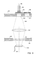
- FIG. 3 A second exemplary embodiment is shown in FIG. 3 .
- the light optical lens 312 is arranged inside the vacuum chamber 400
- the light sensor 313 is arranged outside the vacuum chamber 400 .
- the wall 401 of the vacuum chamber 400 is provided with a window 311 for passing the light 160 generated by the charged particle beam(s) 106 from the converter element 140 , via the light optical lens 312 inside said vacuum chamber 400 , to the sensor 313 outside said vacuum chamber 400 .
- the shielding layer 215 is provided with an opening at least at the position of the window 311 .
- FIG. 4 A third exemplary embodiment is shown in FIG. 4 .
- the light optical lens 322 and the light sensor 323 are arranged inside a compartment 320 .
- the compartment 320 is arranged in an opening in the bottom wall 401 of said vacuum chamber 400 , which is provided with a shielding layer 215 .
- the compartment 320 is part of the bottom wall 401 of the vacuum chamber 400 and is provided with a window 321 at a side facing the target positioning device, in particular the chuck 210 thereof.
- the inside of the compartment 320 is separate from the inside of the vacuum chamber 400 .
- the inside of the compartment 300 can be at ambient pressure, and the light optical lens 322 and/or the sensor 323 do not need to be vacuum compatible.
- the cabling 324 for communicating between the sensor 323 and a control device does not need to be fed through the wall of the vacuum chamber.
- FIG. 5 A fourth exemplary embodiment is shown in FIG. 5 .
- the compartment 330 is arranged in an opening in the bottom wall 401 of said vacuum chamber 400 , which is provided with a shielding layer 215 .
- this embodiment comprising a tube part 334 substantially surrounding a part of the compartment 330 adjacent to the vacuum wall, wherein said tube part 334 extends along said compartment 330 in an outward direction, in particular a downward direction in this example, with respect to the vacuum chamber 400 .
- the tube part 334 comprises at least a layer of ⁇ -metal or permalloy, just as the shielding 215 .
- said tube part 334 extends along said compartment 330 to an inside of the vacuum chamber 400 .
- the tube part 334 comprises a radial extending lip 335 , which is arranged at the inside of the vacuum chamber 400 and extends substantially parallel to the wall of the vacuum chamber 400 around the opening in said wall.
- the radial extending lip 335 at least partially covers the shielding 215 in the vacuum chamber 400 around the opening in said wall of the vacuum chamber 400 , wherein said shielding 215 is arranged between the radial extending lip 335 and the wall 401 .
- the radial extending lip 335 is in contact with the shielding 215 .
- the tube part 334 is tightly arranged between the wall of the vacuum chamber 400 and the circumferential wall of the compartment 330 in order to provide a closure of the vacuum chamber 400 .
- the light optical lens 332 and the sensor 333 are both arranged inside the compartment 330 , and that the compartment 330 is provided with a window 331 at a side facing upwards, toward said chuck 210 .
- FIG. 6 A fifth exemplary embodiment is shown in FIG. 6 .
- the compartment 340 is arranged in an opening in the bottom wall 401 of said vacuum chamber 400 , which is provided with a shielding layer 215 .
- the compartment 340 comprises a flange part 345 which is arranged to connect to the wall of the vacuum chamber 400 to provide a vacuum seal.
- a flange ring 222 is arranged between the wall of said vacuum chamber 400 and said flange part 345 .
- Said flange ring 222 comprises at least a layer of ⁇ -metal or permalloy, just as the shielding 215 of the vacuum chamber 400 .
- said flange ring 222 comprises a first tube part 223 substantially surrounding a part of the compartment 340 adjacent to the wall of the vacuum chamber 400 .
- Said first tube part 223 extends along said compartment 340 in an outward direction, in particular a downward direction, with respect to the vacuum chamber 400 .
- Said first tube part comprises at least a layer of ⁇ -metal or permalloy.
- the flange ring 222 further comprises a second tube part 224 substantially surrounding a part of the compartment 340 adjacent to the wall of the vacuum chamber 400 .
- Said second tube part 224 extends along said compartment 320 in an inward direction with respect to the vacuum chamber 400 .
- the second tube part 224 comprises a radial extending lip 225 which extends substantially parallel to the wall around the opening in said vacuum chamber 400 .
- the wall of the vacuum chamber 400 is provided with a shielding 215 facing the inside of said vacuum chamber 400 .
- the radial extending lip 225 at least partially covers and contacts said shielding 215 around the opening in said wall, wherein said shielding 215 is arranged between the radial extending lip 225 and the wall of the vacuum chamber 400 .
- the second tube part 224 and the radially extending lip 225 comprises at least a layer of ⁇ -metal or permalloy.
- the radial extending lip 225 is in contact with the shielding 215 .
- said flange part 345 of the compartment 340 is arranged at a side of said wall of the vacuum chamber 400 facing to the inside of the vacuum chamber 400 .
- At least the light optical lens 342 is arranged near the window 341 in the compartment 340 , which is substantially open at the bottom side 346 , and that the sensor 343 of the sensor assembly, is arranged outside the compartment 340 and outside the vacuum chamber 400 .
- the compartment 340 of the fifth example having the flange part 345 may also be adapted in order that the sensor 343 can be arranged inside the compartment 340 , as is for example shown in the embodiment of FIGS. 4 and 5 .
- the compartment 320 , 330 of the third and fourth embodiments may also be adapted on order to arrange the sensor 323 , 333 outside the compartment 320 , 330 , as for example shown in the embodiment in FIG. 6 .
Landscapes
- Chemical & Material Sciences (AREA)
- Analytical Chemistry (AREA)
- Exposure And Positioning Against Photoresist Photosensitive Materials (AREA)
- Electron Sources, Ion Sources (AREA)
- Electron Beam Exposure (AREA)
Abstract
Description
-
- an
illumination optics module 201 including the chargedparticle beam source 101 andbeam collimating system 102, - an aperture array and
condenser lens module 202 including aperture array 103 and condenser lens array 104, - a
beam switching module 203 including beamblanker array 105, and -
projection optics module 204 including beam stop array 108, beam deflector array 109, and projection lens arrays 110.
- an
Claims (25)
Priority Applications (1)
| Application Number | Priority Date | Filing Date | Title |
|---|---|---|---|
| US14/581,728 US9153415B2 (en) | 2013-12-24 | 2014-12-23 | Charged particle lithography system with sensor assembly |
Applications Claiming Priority (4)
| Application Number | Priority Date | Filing Date | Title |
|---|---|---|---|
| NL2012029 | 2013-12-24 | ||
| NL2012029A NL2012029C2 (en) | 2013-12-24 | 2013-12-24 | Charged particle lithography system with sensor assembly. |
| US201361921002P | 2013-12-26 | 2013-12-26 | |
| US14/581,728 US9153415B2 (en) | 2013-12-24 | 2014-12-23 | Charged particle lithography system with sensor assembly |
Publications (2)
| Publication Number | Publication Date |
|---|---|
| US20150179398A1 US20150179398A1 (en) | 2015-06-25 |
| US9153415B2 true US9153415B2 (en) | 2015-10-06 |
Family
ID=50391337
Family Applications (1)
| Application Number | Title | Priority Date | Filing Date |
|---|---|---|---|
| US14/581,728 Active US9153415B2 (en) | 2013-12-24 | 2014-12-23 | Charged particle lithography system with sensor assembly |
Country Status (6)
| Country | Link |
|---|---|
| US (1) | US9153415B2 (en) |
| JP (1) | JP6393759B2 (en) |
| CN (1) | CN105849854B (en) |
| NL (1) | NL2012029C2 (en) |
| TW (1) | TWI644179B (en) |
| WO (1) | WO2015099527A1 (en) |
Families Citing this family (1)
| Publication number | Priority date | Publication date | Assignee | Title |
|---|---|---|---|---|
| JP6834817B2 (en) * | 2016-08-08 | 2021-02-24 | 株式会社ニューフレアテクノロジー | Aperture for multi-beam inspection, beam inspection device for multi-beam, and multi-charged particle beam drawing device |
Citations (10)
| Publication number | Priority date | Publication date | Assignee | Title |
|---|---|---|---|---|
| US6218671B1 (en) * | 1998-08-31 | 2001-04-17 | Nikon Corporation | On-line dynamic corrections adjustment method |
| EP1505630A2 (en) | 2003-08-06 | 2005-02-09 | Canon Kabushiki Kaisha | Charged particle beam exposure method and apparatus and device manufacturing method using the apparatus |
| JP2005347054A (en) | 2004-06-02 | 2005-12-15 | Hitachi High-Technologies Corp | Electron beam detector, electron beam writing method and electron beam writing apparatus using the same |
| US20070057204A1 (en) * | 2005-09-15 | 2007-03-15 | Pieter Kruit | Lithography system, sensor and measuring method |
| US20090290139A1 (en) * | 2008-05-21 | 2009-11-26 | Asml Netherlands B.V. | Substrate table, sensor and method |
| US20120069317A1 (en) * | 2010-09-20 | 2012-03-22 | Jerry Peijster | Lithography system arranged on a foundation, and method for arranging a lithography system on said foundation |
| WO2013037802A1 (en) | 2011-09-12 | 2013-03-21 | Mapper Lithography Ip B.V. | Vacuum chamber with base plate |
| WO2013171177A1 (en) | 2012-05-14 | 2013-11-21 | Mapper Lithography Ip B.V. | Method for determining a beamlet position and method for determining a distance between two beamlets in a multi-beamlet exposure apparatus |
| US20150001423A1 (en) * | 2012-01-24 | 2015-01-01 | Mapper Lithography Ip B.V. | Device for spot size measurement at wafer level using a knife edge and a method for manufacturing such a device |
| US20150109601A1 (en) * | 2012-03-08 | 2015-04-23 | Mapper Lithography Ip B.V. | Charged particle lithography system with alignment sensor and beam measurement sensor |
Family Cites Families (6)
| Publication number | Priority date | Publication date | Assignee | Title |
|---|---|---|---|---|
| US6353231B1 (en) * | 1998-08-31 | 2002-03-05 | Nikon Corporation | Pinhole detector for electron intensity distribution |
| NL1027462C2 (en) * | 2004-11-09 | 2006-05-10 | Koninkl Philips Electronics Nv | Method for locating fluorescent markers. |
| CN101248505B (en) * | 2005-07-08 | 2010-12-15 | 耐克斯金思美控股公司 | Apparatus and methods for the manufacture of controlled particle beams |
| KR101433385B1 (en) | 2005-09-15 | 2014-08-26 | 마퍼 리쏘그라피 아이피 비.브이. | Lithography systems, sensors and measuring methods |
| CN101366095B (en) * | 2005-12-02 | 2010-11-10 | 阿利斯公司 | Ion source, system and method |
| JP5352262B2 (en) * | 2009-02-06 | 2013-11-27 | 株式会社日立ハイテクノロジーズ | Charged particle beam equipment |
-
2013
- 2013-12-24 NL NL2012029A patent/NL2012029C2/en active
-
2014
- 2014-12-22 JP JP2016533724A patent/JP6393759B2/en active Active
- 2014-12-22 WO PCT/NL2014/050897 patent/WO2015099527A1/en not_active Ceased
- 2014-12-22 CN CN201480070999.5A patent/CN105849854B/en active Active
- 2014-12-23 US US14/581,728 patent/US9153415B2/en active Active
- 2014-12-23 TW TW103144937A patent/TWI644179B/en active
Patent Citations (10)
| Publication number | Priority date | Publication date | Assignee | Title |
|---|---|---|---|---|
| US6218671B1 (en) * | 1998-08-31 | 2001-04-17 | Nikon Corporation | On-line dynamic corrections adjustment method |
| EP1505630A2 (en) | 2003-08-06 | 2005-02-09 | Canon Kabushiki Kaisha | Charged particle beam exposure method and apparatus and device manufacturing method using the apparatus |
| JP2005347054A (en) | 2004-06-02 | 2005-12-15 | Hitachi High-Technologies Corp | Electron beam detector, electron beam writing method and electron beam writing apparatus using the same |
| US20070057204A1 (en) * | 2005-09-15 | 2007-03-15 | Pieter Kruit | Lithography system, sensor and measuring method |
| US20090290139A1 (en) * | 2008-05-21 | 2009-11-26 | Asml Netherlands B.V. | Substrate table, sensor and method |
| US20120069317A1 (en) * | 2010-09-20 | 2012-03-22 | Jerry Peijster | Lithography system arranged on a foundation, and method for arranging a lithography system on said foundation |
| WO2013037802A1 (en) | 2011-09-12 | 2013-03-21 | Mapper Lithography Ip B.V. | Vacuum chamber with base plate |
| US20150001423A1 (en) * | 2012-01-24 | 2015-01-01 | Mapper Lithography Ip B.V. | Device for spot size measurement at wafer level using a knife edge and a method for manufacturing such a device |
| US20150109601A1 (en) * | 2012-03-08 | 2015-04-23 | Mapper Lithography Ip B.V. | Charged particle lithography system with alignment sensor and beam measurement sensor |
| WO2013171177A1 (en) | 2012-05-14 | 2013-11-21 | Mapper Lithography Ip B.V. | Method for determining a beamlet position and method for determining a distance between two beamlets in a multi-beamlet exposure apparatus |
Also Published As
| Publication number | Publication date |
|---|---|
| TWI644179B (en) | 2018-12-11 |
| CN105849854B (en) | 2018-02-13 |
| TW201535062A (en) | 2015-09-16 |
| JP2017504187A (en) | 2017-02-02 |
| WO2015099527A1 (en) | 2015-07-02 |
| JP6393759B2 (en) | 2018-09-19 |
| NL2012029C2 (en) | 2015-06-26 |
| CN105849854A (en) | 2016-08-10 |
| US20150179398A1 (en) | 2015-06-25 |
Similar Documents
| Publication | Publication Date | Title |
|---|---|---|
| CN111656169B (en) | Position feedback for multi-beam particle detectors | |
| US9812288B2 (en) | Sample holder with light emitting and transferring elements for a charged particle beam apparatus | |
| TWI662582B (en) | Scanning electron microscopy apparatus andmethod for imaging of a photomask through apellicle | |
| KR102184032B1 (en) | System and method for drift compensation of electron beam-based characterization tool | |
| KR102107559B1 (en) | Using multiple sources/detectors for high-throughput x-ray topography measurement | |
| TWI614503B (en) | Inspection system using scanning electron microscope | |
| KR102190328B1 (en) | Coaxial mask alignment device, photolithographic apparatus and alignment method | |
| JP2008197094A (en) | Device for measuring position of at least one structure on object, method of using lighting system in measuring device and method for using protective gas in measuring device | |
| KR102544677B1 (en) | Electron Beam Inspection Equipment and Electron Beam Inspection Assemblies for Semiconductor Devices | |
| JP2022505064A (en) | Multi-beam electronic characterization tool with telecentric lighting | |
| US9153415B2 (en) | Charged particle lithography system with sensor assembly | |
| JP5932023B2 (en) | Lithographic system for processing at least part of a target | |
| US6552341B1 (en) | Installation and method for microscopic observation of a semiconductor electronic circuit | |
| CN113539769B (en) | Electron beam imaging equipment for realizing coaxiality and realization method | |
| JP6214903B2 (en) | Inspection device | |
| JP6931592B2 (en) | Charged particle beam device | |
| KR101727196B1 (en) | Infrared-electron correlative microscope | |
| US12387905B2 (en) | Apparatus and method for detecting one or more scanning charged particle beams | |
| WO2023196133A1 (en) | Extra tall target metrology | |
| US9091525B2 (en) | Method for focusing an object plane and optical assembly | |
| KR102936003B1 (en) | Design Aid Wide Field of View Measurement | |
| US12619162B2 (en) | Extra tall target metrology | |
| CN110709960A (en) | Charged Particle Beam Device | |
| EP2458617A1 (en) | Electron microscope with assistive locating apparatus | |
| KR101237528B1 (en) | Apparatus for Analyzing Optical Characteristic of Panel Display |
Legal Events
| Date | Code | Title | Description |
|---|---|---|---|
| AS | Assignment |
Owner name: MAPPER LITHOGRAPHY IP B.V., NETHERLANDS Free format text: ASSIGNMENT OF ASSIGNORS INTEREST;ASSIGNOR:SCHEFFERS, PAUL IJMERT;REEL/FRAME:036116/0718 Effective date: 20150211 |
|
| STCF | Information on status: patent grant |
Free format text: PATENTED CASE |
|
| MAFP | Maintenance fee payment |
Free format text: PAYMENT OF MAINTENANCE FEE, 4TH YR, SMALL ENTITY (ORIGINAL EVENT CODE: M2551); ENTITY STATUS OF PATENT OWNER: SMALL ENTITY Year of fee payment: 4 |
|
| AS | Assignment |
Owner name: WITTEKAMP, J.J., NETHERLANDS Free format text: COURT APPOINTMENT;ASSIGNORS:MAPPER LITHOGRAPHY HOLDING B.V.;MAPPER LITHOGRAPHY IP B.V.;MAPPER LITHOGRAPHY B.V.;REEL/FRAME:049104/0734 Effective date: 20181228 Owner name: ASML NETHERLANDS B.V., NETHERLANDS Free format text: ASSIGNMENT OF ASSIGNORS INTEREST;ASSIGNOR:WITTEKAMP, J.J.;REEL/FRAME:049296/0606 Effective date: 20190206 |
|
| FEPP | Fee payment procedure |
Free format text: ENTITY STATUS SET TO UNDISCOUNTED (ORIGINAL EVENT CODE: BIG.); ENTITY STATUS OF PATENT OWNER: LARGE ENTITY |
|
| MAFP | Maintenance fee payment |
Free format text: PAYMENT OF MAINTENANCE FEE, 8TH YEAR, LARGE ENTITY (ORIGINAL EVENT CODE: M1552); ENTITY STATUS OF PATENT OWNER: LARGE ENTITY Year of fee payment: 8 |