US9141118B2 - Switching current synthesis circuit for power converter - Google Patents
Switching current synthesis circuit for power converter Download PDFInfo
- Publication number
- US9141118B2 US9141118B2 US13/693,707 US201213693707A US9141118B2 US 9141118 B2 US9141118 B2 US 9141118B2 US 201213693707 A US201213693707 A US 201213693707A US 9141118 B2 US9141118 B2 US 9141118B2
- Authority
- US
- United States
- Prior art keywords
- signal
- current
- switching
- discharge
- inductor
- Prior art date
- Legal status (The legal status is an assumption and is not a legal conclusion. Google has not performed a legal analysis and makes no representation as to the accuracy of the status listed.)
- Active, expires
Links
Images


Classifications
-
- G—PHYSICS
- G05—CONTROLLING; REGULATING
- G05F—SYSTEMS FOR REGULATING ELECTRIC OR MAGNETIC VARIABLES
- G05F1/00—Automatic systems in which deviations of an electric quantity from one or more predetermined values are detected at the output of the system and fed back to a device within the system to restore the detected quantity to its predetermined value or values, i.e. retroactive systems
- G05F1/10—Regulating voltage or current
- G05F1/12—Regulating voltage or current wherein the variable actually regulated by the final control device is ac
- G05F1/40—Regulating voltage or current wherein the variable actually regulated by the final control device is ac using discharge tubes or semiconductor devices as final control devices
- G05F1/44—Regulating voltage or current wherein the variable actually regulated by the final control device is ac using discharge tubes or semiconductor devices as final control devices semiconductor devices only
-
- H—ELECTRICITY
- H02—GENERATION; CONVERSION OR DISTRIBUTION OF ELECTRIC POWER
- H02M—APPARATUS FOR CONVERSION BETWEEN AC AND AC, BETWEEN AC AND DC, OR BETWEEN DC AND DC, AND FOR USE WITH MAINS OR SIMILAR POWER SUPPLY SYSTEMS; CONVERSION OF DC OR AC INPUT POWER INTO SURGE OUTPUT POWER; CONTROL OR REGULATION THEREOF
- H02M1/00—Details of apparatus for conversion
- H02M1/42—Circuits or arrangements for compensating for or adjusting power factor in converters or inverters
- H02M1/4208—Arrangements for improving power factor of AC input
- H02M1/4225—Arrangements for improving power factor of AC input using a non-isolated boost converter
-
- H—ELECTRICITY
- H02—GENERATION; CONVERSION OR DISTRIBUTION OF ELECTRIC POWER
- H02M—APPARATUS FOR CONVERSION BETWEEN AC AND AC, BETWEEN AC AND DC, OR BETWEEN DC AND DC, AND FOR USE WITH MAINS OR SIMILAR POWER SUPPLY SYSTEMS; CONVERSION OF DC OR AC INPUT POWER INTO SURGE OUTPUT POWER; CONTROL OR REGULATION THEREOF
- H02M3/00—Conversion of dc power input into dc power output
- H02M3/02—Conversion of dc power input into dc power output without intermediate conversion into ac
- H02M3/04—Conversion of dc power input into dc power output without intermediate conversion into ac by static converters
- H02M3/10—Conversion of dc power input into dc power output without intermediate conversion into ac by static converters using discharge tubes with control electrode or semiconductor devices with control electrode
- H02M3/145—Conversion of dc power input into dc power output without intermediate conversion into ac by static converters using discharge tubes with control electrode or semiconductor devices with control electrode using devices of a triode or transistor type requiring continuous application of a control signal
- H02M3/155—Conversion of dc power input into dc power output without intermediate conversion into ac by static converters using discharge tubes with control electrode or semiconductor devices with control electrode using devices of a triode or transistor type requiring continuous application of a control signal using semiconductor devices only
- H02M3/156—Conversion of dc power input into dc power output without intermediate conversion into ac by static converters using discharge tubes with control electrode or semiconductor devices with control electrode using devices of a triode or transistor type requiring continuous application of a control signal using semiconductor devices only with automatic control of output voltage or current, e.g. switching regulators
-
- Y—GENERAL TAGGING OF NEW TECHNOLOGICAL DEVELOPMENTS; GENERAL TAGGING OF CROSS-SECTIONAL TECHNOLOGIES SPANNING OVER SEVERAL SECTIONS OF THE IPC; TECHNICAL SUBJECTS COVERED BY FORMER USPC CROSS-REFERENCE ART COLLECTIONS [XRACs] AND DIGESTS
- Y02—TECHNOLOGIES OR APPLICATIONS FOR MITIGATION OR ADAPTATION AGAINST CLIMATE CHANGE
- Y02B—CLIMATE CHANGE MITIGATION TECHNOLOGIES RELATED TO BUILDINGS, e.g. HOUSING, HOUSE APPLIANCES OR RELATED END-USER APPLICATIONS
- Y02B70/00—Technologies for an efficient end-user side electric power management and consumption
- Y02B70/10—Technologies improving the efficiency by using switched-mode power supplies [SMPS], i.e. efficient power electronics conversion e.g. power factor correction or reduction of losses in power supplies or efficient standby modes
-
- Y02B70/126—
-
- Y—GENERAL TAGGING OF NEW TECHNOLOGICAL DEVELOPMENTS; GENERAL TAGGING OF CROSS-SECTIONAL TECHNOLOGIES SPANNING OVER SEVERAL SECTIONS OF THE IPC; TECHNICAL SUBJECTS COVERED BY FORMER USPC CROSS-REFERENCE ART COLLECTIONS [XRACs] AND DIGESTS
- Y02—TECHNOLOGIES OR APPLICATIONS FOR MITIGATION OR ADAPTATION AGAINST CLIMATE CHANGE
- Y02P—CLIMATE CHANGE MITIGATION TECHNOLOGIES IN THE PRODUCTION OR PROCESSING OF GOODS
- Y02P80/00—Climate change mitigation technologies for sector-wide applications
- Y02P80/10—Efficient use of energy, e.g. using compressed air or pressurized fluid as energy carrier
Definitions
- the invention relates to a switching current synthesis circuit, and more particularly to a switching current synthesis circuit for a power converter operating in a continuous current mode (CCM) and a discontinuous current mode (DCM).
- CCM continuous current mode
- DCM discontinuous current mode
- FIG. 1 shows a prior art of a PFC power converter. It includes a resistor 31 coupled to sense a switching current I L of an inductor 20 .
- the resistor 31 is coupled in the charging and discharging path of the inductor 20 .
- the current flowing through the resistor 31 is an average value of the switching current I L . Therefore, the circuit scheme shown in the FIG. 1 is called as “average-current control”.
- the drawback of the average-current control scheme has higher power consumption in the resistor 31 .
- the control circuit comprises a PWM circuit, a sample circuit, and emulation circuit.
- the PWM circuit generates a switching signal for switching an inductor and generating a switching current of the inductor in response to a current feedback signal.
- the sample circuit is coupled to sample a switching current signal into a capacitor during an on time of the switching signal.
- the emulation circuit generates a discharge current couple to discharge the capacitor during an off time of the switching signal for generating the current feedback signal.
- the switching current signal is correlated to the switching current of the inductor, and the discharge current is generated in response to an input voltage of the inductor, an output voltage of the power converter, and the on time of the switching signal.
- An exemplary embodiment of a method for controlling a power converter comprises steps of generating a switching signal for switching an inductor and generating a switching current of the inductor in response to a current feedback signal; sampling a switching current signal into a capacitor during an on time of the switching signal; generating a discharge current to discharge the capacitor during an off time of the switching signal for generating an emulated switching current signal.
- the switching current signal is correlated to the switching current of the inductor, the discharge current is generated in response to an input voltage of the inductor, an output voltage of the power converter, and the on time of the switching signal, and the emulated switching current signal is coupled to generate the current feedback signal.
- FIG. 1 shows a prior art of a PFC power converter
- FIG. 2 shows an exemplary embodiment of a PFC power converter
- FIG. 2A shows discontinuous current mode (DCM) waveforms of a switching signal, a switching current, and a switching current signal of the PFC power converter in FIG. 2 ;
- DCM discontinuous current mode
- FIG. 2B shows continuous current mode (CCM) waveforms of a switching signal, a switching current, and a switching current signal of the PFC power converter in FIG. 2 ;
- FIG. 3 is an exemplary embodiment of a control circuit of the PFC power converter in FIG. 2 ;
- FIG. 4 is an exemplary embodiment of a synthesis circuit of the control circuit in FIG. 3 ;
- FIG. 5 shows waveforms of a synthesis current signal, a pulse signal, a switching current signal, a switching signal, and a signal of the power converter in FIG. 2 in a DCM operation;
- FIG. 6 shows the waveforms of a synthesis current signal, a pulse signal, a switching current signal, a switching signal, and a signal of the power converter in FIG. 2 in a CCM operation.
- FIG. 7 is an exemplary embodiment of an emulation circuit of the synthesis circuit in FIG. 4 ;
- FIG. 8 is an exemplary embodiment of a detection circuit of the control circuit in FIG. 3 ;
- FIG. 9 is an exemplary embodiment of a circuit of the detection circuit in FIG. 8 ;
- FIG. 10 shows an exemplary embodiment of a PWM circuit of the control circuit in FIG. 3 ;
- FIG. 11 shows waveforms of a ramp signal, a pulse signal, and a switching signal of the PWM circuit in FIG. 10 .
- FIG. 2 shows an exemplary embodiment of a power factor correction (PFC) power converter.
- the PFC power converter comprises a current sense resistor 35 coupled to sample a switching current I L of an inductor 20 and generate a switching current signal V S coupled to a PFC control circuit 100 .
- the FPC control circuit 100 will generate a switching signal S W to switch the inductor 20 and generate the switching current I L via a power transistor 30 .
- the switching current I L further generate the switching current signal V S at the resistor 35 , which develops a close current loop for the PFC control.
- a capacitor 53 is used for frequency compensation of the current loop.
- a resistor 50 is coupled to detect an input voltage V IN of the inductor 20 and generate an input-voltage signal I AC coupled to the PFC control circuit 100 .
- the input voltage V IN is obtained from an alternating current (AC) mains V AC through a bridge rectifier 10 .
- the switching current I L of the inductor 20 is discharged to an output capacitor 45 via a rectifier 40 to generate an output voltage V O .
- Resistors 41 and 22 form a voltage divider coupled to the output of the PFC power converter to detect the output voltage V O and generate a signal V FB coupled to the PFC control circuit 100 for regulating of the output voltage V O .
- the signals V FB , S W , and the output voltage V O develop a voltage loop for the PFC control.
- a capacitor 51 is used for frequency compensation of the voltage loop.
- the current sense resistor 35 can only detect the charge signal of the switching current I L during on time of the power transistor 30 .
- the object of this invention is to emulate the discharge signal of the switching current I L and provide an accurate synthesis for the switching current signal V S during the off time of the power transistor 30 . Because the inductance of the inductor 20 is changed in response to the change of the operating temperature and the change of the switching current I L , the synthesis discharge signal must be correlated to the charge signal of the switching current I L .
- FIG. 2A shows discontinuous current mode (DCM) waveforms of the switching signal S W , the switching current I L , and the switching current signal V S .
- the switching current I L of the inductor 20 is fully discharged before the start of the next switching cycle.
- FIG. 2B shows continuous current mode (CCM) waveforms of the switching signal S W , the switching current I L , and the switching current signal V S .
- the switching current I L of the inductor 20 still has a current I 1 existed in the inductor 20 before the start of the next switching cycle.
- the slope of the charge signal (charge current) of the switching current I L is equal to the slope of the discharge signal (discharge current) of the switching current I L , which can be expressed as:
- T ON is the on time of the switching signal S W , also shown in FIGS. 2A and 2B .
- T DS is the discharge time of the inductor 20 .
- Equation (1) shows the switching current I L operated in a DCM, wherein T OFF >T DS , and T OFF is the off time of the switching signal S W .
- Equation (2) shows the switching current I L operated in a CCM, wherein T DS >T OFF . Therefore, the current I 1 is still existed in the inductor 20 when the next switching signal S W starts.
- FIG. 3 is an exemplary embodiment of the PFC control circuit 100 according to the present invention.
- a transconductance amplifier (G M ) 110 is coupled to receive the signal V FB and a reference signal V R for generating a voltage loop signal V EA .
- the capacitor 51 is coupled to the voltage loop signal V EA for the frequency compensation of the voltage loop.
- a multiplier-divider 130 generates a switching-current command signal V M in accordance with the voltage loop signal V EA and the input-voltage signal I AC .
- the skill of the multiplier-divider 130 can be found in some prior arts, such as U.S. Pat. No. 7,057,440 titled “Multiplier-divider circuit for a PFC controller”.
- a synthesis circuit (I AV ) 150 is couple to receive the switching current signal V S for generating a synthesis current signal V I (also referred to as a current feedback signal).
- the switching current signal V S is only available during the on time T ON of the switching signal S W . This is because when the power transistor 30 is turned off (shown in FIG. 2 ), the switching current signal V S has a zero value during the off time of the switching signal S W , which is shown in FIG. 2A and FIG. 2B .
- the synthesis circuit 150 is utilized to sample the switching current signal V S and emulate the switching current I L during the discharge period of the inductor 20 .
- the synthesis current signal V I includes the switching current signal V S in the on time of the switching signal S W and the discharge signal in the off time of the switching signal S W .
- the signal V FB , the input-voltage signal I AC , and the switching signal S W are coupled to the synthesis circuit 150 for emulating the discharge signal.
- the synthesis circuit 150 further generates signals V X , I VO and I VIN , wherein the signals I VO and I VIN are coupled to a detection circuit (DET) 200 .
- the signal I VO is correlated to the level of the output voltage V O .
- the signal I VIN is correlated to the level of the input voltage V IN .
- the signal (also referred to as a first signal) V X is correlated to the switching current signal V S .
- the detection circuit 200 is coupled to receive the switching signal S W , the input-voltage signal I AC , and a pulse signal PLS for generating a control signal N N N O .
- the control signal N N N O is coupled to modulate the discharge signal of the synthesis current signal V I in response to the signal V X .
- a transconductance amplifier (G M ) 120 receives the switching-current command signal V M and the synthesis current signal V I to generate a current loop signal I EA .
- the capacitor 53 is coupled to the current loop signal I EA (shown in FIG. 2 ) for the frequency compensation of the current loop compensation.
- a pulse width modulation (PWM) circuit (PWM) 300 generates the switching signal S W in accordance with the current loop signal I EA .
- the PWM circuit 300 further generates the pulse signal PLS coupled to the detection circuit 200 .
- FIG. 4 is an exemplary embodiment of the synthesis circuit 150 according to the present invention.
- a positive terminal of an amplifier 160 receives the switching current signal V S , and a negative terminal thereof is coupled to a ground via a resistor 161 .
- a resistor 162 is coupled between the negative terminal and an output of the amplifier 160 .
- the amplifier 160 generates the signal V X at the output of the amplifier 160 in accordance with the switching current signal V S .
- the amplifier 160 further generates the synthesis current signal V I by sampling the switching current signal V S via a resistor 163 and a switch 165 during the on time of the switching signal S W .
- the synthesis current signal V I is hold in a capacitor 167 after the switch 165 is turned off.
- An emulation circuit 170 generates a discharge current I DS in response to the signals V FB , the input-voltage signal I AC , and the control signal N N N O .
- the discharge current I DS is coupled to discharge the capacitor 167 for emulating the discharge signal of the synthesis current signal V I during the off time of the switching signal S W .
- the amplifier 160 , the resistors 161 - 163 , the switch 165 , and the capacitor 167 form a sample circuit.
- the sample circuit samples the switching current signal into the capacitor 167 during the on time of the switching signal
- the emulation circuit 170 further generates the signals I VO and I VIN coupled to the detection circuit 200 .
- the emulation circuit 170 is developed for generating the discharge current I DS .
- the detail operation for the discharge (demagnetizing) of the inductor can be found in some prior arts, such as U.S. Pat. No. 7,471,523 titled “Method and apparatus for detecting demagnetizing time of magnetic device”.
- Equation (3) shows the discharge current I DS .
- T DS T ON ⁇ k ⁇ V IN ( V O - V IN ) ( 3 )
- k is a constant, which represents a slope of the discharge signal.
- the discharge current I DS is correlated to the discharge time T DS .
- the input-voltage signal I AC is correlated to the input voltage V IN .
- the signal V FB is correlated to the output voltage V O .
- the discharge current I DS associated with the capacitance of the capacitor 167 determines the discharge time T DS .
- FIG. 5 shows the waveforms of the synthesis current signal V I , the pulse signal PLS, the switching current signal V S , the switching signal S W , and a signal S D operated in the DCM.
- the slope of the discharge signal of the synthesis current signal V I is modulated in accordance with the signal S D (a discharge signal developed in accordance with Equation (3)).
- the signal S D is enabled (logic-high) in response to the turned-off state of the switching signal S W .
- the synthesis current signal V I will be discharged to a zero value when the signal S D is disabled (logic-low).
- a sample-signal SMP 1 indicates the end of the discharge time T DS (the signal S D is disabled). If the synthesis current signal V I cannot be discharged to the zero, then the control signal N N N O will be modulated to increase the discharge slope of the synthesis current signal V I .
- FIG. 6 shows the waveforms of the synthesis current signal V I , the pulse signal PLS, the switching current signal V S , the switching signal S W , and the signal S D operated in the CCM.
- the slope of the discharge signal of the synthesis current signal V I is generated in accordance with the value by sampling the switching current signal V S (by a sample-signal SMP 2 ).
- the sample-signal SMP 2 is applied to sample the initial value of the switching current signal V S when the switching signal S W is turned on.
- a short time-delay is required to avoid the turned-on spike of the switching current signal V S .
- the initial value of the switching current signal V S indicates the continuous current I 1 shown in FIG. 2B .
- the signal S D is still enabled when the switching signal S W is turned on in the CCM operation.
- the signal S D will be disabled in response to the turned-on state of the switching signal S W .
- the synthesis current signal V I will be discharged to the initial value of the switching current signal V S in response to the pulse signal PLS.
- the pulse signal PLS is developed to indicate the end of the switching cycle.
- the sample-signal SMP 1 is utilized to sample the value of the synthesis current signal V I at the end of the switching cycle. If the sampled value of the synthesis current signal V I is not equal to the initial value of the switching current signal V S , then the control signal N N N O will be modulated to change the discharge slope of the synthesis current signal V I .
- FIG. 7 is an exemplary embodiment of the emulation circuit 170 according to the present invention.
- An amplifier 171 , a resistor 173 , and a transistor 172 develop a V-to-I converter for generating a current I 172 in accordance with the signal V FB .
- Transistors 180 , 181 , 182 , 185 , and 186 form a first current mirror to generate the signal I VO and a current I 182 .
- Transistors 192 , 193 , and 194 form a second current mirror to generate the signal I VIN and a current I 192 .
- Transistors 195 and 196 ⁇ 199 develop a third current mirror generates the discharge current I DS in response to the current I 182 and the current I 192 .
- the discharge current I DS is modulated by the control signal N N N O via switches 177 ⁇ 179 .
- R 41 is the resistance of the resistor 41 .
- R 42 is the resistance of the resistor 42 .
- R 50 is the resistance of the resistor 50 .
- R 173 is the resistance of the resistor 173 .
- k1, k2 and K N are current mirror ratio;
- Equation (5) The discharge current I DS shown in Equation (4) can be expressed as Equation (5).
- I DS K N ⁇ ⁇ [ V O ⁇ R 42 R 41 + R 42 ] ⁇ R 173 ⁇ ⁇ k ⁇ ⁇ 1 - ( V IN R 50 ⁇ k ⁇ ⁇ 2 ) ( 5 )
- k1, k2 and K N are current mirror ratios
- the constant K N is determined by the control signal N N N O via the switches 177 ⁇ 179 . Changing the constant K N will change the slope of the discharge current I DS .
- the charge slope of the switching current signal V S should be equal to the discharge slope of the synthesis current signal V I , which is shown in Equation (6).
- Equation (5) Equation (6) can be rewritten as Equation (7) and Equation (8),
- L 20 is the inductance of the inductor 20 .
- C 167 is the capacitance of the capacitor 167 .
- k A ( 1 L 20 ⁇ R 35 ⁇ k ⁇ ⁇ 3 )
- Equation (8) can be rewritten as Equation (3). Changing the constant K N will change the constant k.
- T DS T ON ⁇ k ⁇ V IN ( V O - V IN )
- FIG. 8 is an exemplary embodiment of the detection circuit 200 according to the present invention.
- the detection circuit 200 is developed to generate the control signal N N N O and detect the operation of the DCM or CCM.
- the detection circuit 200 will determine the sample-signals SMP 1 and SMP 2 (shown in FIG. 5 and FIG. 6 ).
- the signal I VIN is coupled to charge a capacitor 230 via transistors 210 , 211 , 215 , and 216 and a switch 220 during on time of the switching signal S W .
- the switching signal S W is turned off, the signal I VO and the signal I VIN are coupled to discharge the capacitor 230 via a switch 225 and a transistor 217 during the discharge time T DS .
- the discharge signal S D controls the switch 225 .
- the enabling of the discharge signal S D indicates the discharge time T DS .
- the switching signal S W controls the switch 220 .
- a circuit 245 generates a pulse signal S P according to the rising edge of the switching signal S W , and the pulse signal S P is coupled to discharge the capacitor 230 through a transistor 246 .
- a saw signal S AW is thus generated in the capacitor 230 in response to the switching signal S W and the discharge signal S D .
- a comparator 240 is utilized to compare the saw signal S AW with a threshold V T .
- the output of the comparator 240 is coupled to enable the discharge signal S D via an AND gate 242 and an inverter 241 when the switching signal S W is turned off and the saw signal S AW is higher than the threshold V T .
- the discharge signal S D , the switching signal S W , the signal V X , and the pulse signal PLS are coupled to a circuit 250 for generating an up-count signal S U .
- the up-count signal S U and the pulse signal PLS are coupled to a flip-flop 248 for generating an up/down signal U/D.
- the rising edge of the pulse signal PLS is applied to enable of the switching signal S W and latch the status of the up-count signal S U .
- the up/down signal U/D is coupled to a counter 249 for generating the control signal N N N O in response to the falling edge of the switching signal S W .
- the control signal N N N O will be increased to change the slope of the discharge signal of the synthesis current signal V I when the up/down signal U/D is enabled (logic-high). Equation (9) shows the operation of the detection circuit 200 .
- I VIN ⁇ ka ) ⁇ T ON ( I VO ⁇ I VIN ⁇ kb ) ⁇ T DS (9)
- Equation (10) will be same as Equation (7).
- Equation (7) ka, kb, kc, kd, ke are the constant determined by the circuit parameters.
- FIG. 9 is an exemplary embodiment of the circuit 250 according to the present invention.
- the circuit is used for generating a CCM signal S CCM (mode signal) when the switching current I L is operated in CCM and generating the up-count signal S U .
- the discharge signal S D and the pulse signal PLS are coupled to generate the sample-signal SMP 1 via an AND gate 253 .
- the sample-signal SMP 1 is coupled to sample the synthesis current signal V I into a capacitor 271 through a buffer 251 , a resistor 252 , and a switch 267 for generating a signal V IH .
- the rising edge of the switching signal S W generates a pulse sample-signal SMP 2 via a pulse generator 256 .
- the sample-signal SMP 2 is coupled to sample the signal V X into a capacitor 272 via a switch 269 for generating a signal V XH .
- the signal V X is correlated to the switching current signal V S .
- the discharge signal S D and the pulse signal PLS are coupled to a flip-flop 263 to generate the CCM signal S CCM . If the discharge signal S D (discharge time T DS ) is still enable (available) in response to the rising edge of the pulse signal PLS (the start of the next switching cycle), then it indicates the CCM operation.
- the CCM signal S CCM is coupled to a DCM/CCM multiplexer for generating the up-count signal SU.
- An inverter 283 , an OR gate 290 , and AND gates 286 and 285 develop the DCM/CCM multiplexer.
- the signal V IH and a threshold V T2 are coupled to a comparator 280 to check if the signal V IH is higher than a zero value when the switching current I L is operated in the DCM.
- the output of the comparator 280 is coupled to the input of the AND gate 285 .
- the signal V IH and the signal V XH are coupled to a comparator 281 to check if the signal V IH is higher than the signal V XH (the initial value of the signal V S ) when the switching current I L is operated in the CCM.
- the output of the comparator 281 is coupled to the input of the AND gate 286 .
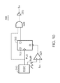
- FIG. 10 shows an exemplary embodiment of the PWM circuit 300 .
- An oscillator (OSC) 310 generates the pulse signal PLS and a ramp signal RMP.
- the pulse signal PLS is coupled to generate the switching signal S W and provide a dead-time for the switching signal S W .
- the ramp signal RMP is coupled to compare with the signal I EA for the reset of a flip-flop 350 via a comparator 320 .
- the flip-flop 350 generates the switching signal S W through an AND gate 360 and an output buffer 365 .
- FIG. 11 shows the waveforms of the ramp signal RMP, the pulse signal PLS, and the switching signal S W .
Abstract
Description
(I VIN ×ka)×T ON=(I VO −I VIN ×kb)×T DS (9)
(V IN ×kc)×T ON=(V O ×kd−V IN ×ke)×T DS (10)
set the kd=ke and
then Equation (10) will be same as Equation (7).
where ka, kb, kc, kd, ke are the constant determined by the circuit parameters.
Claims (16)
Priority Applications (1)
| Application Number | Priority Date | Filing Date | Title |
|---|---|---|---|
| US13/693,707 US9141118B2 (en) | 2011-12-07 | 2012-12-04 | Switching current synthesis circuit for power converter |
Applications Claiming Priority (2)
| Application Number | Priority Date | Filing Date | Title |
|---|---|---|---|
| US201161567864P | 2011-12-07 | 2011-12-07 | |
| US13/693,707 US9141118B2 (en) | 2011-12-07 | 2012-12-04 | Switching current synthesis circuit for power converter |
Publications (2)
| Publication Number | Publication Date |
|---|---|
| US20130147452A1 US20130147452A1 (en) | 2013-06-13 |
| US9141118B2 true US9141118B2 (en) | 2015-09-22 |
Family
ID=48109323
Family Applications (1)
| Application Number | Title | Priority Date | Filing Date |
|---|---|---|---|
| US13/693,707 Active 2033-08-21 US9141118B2 (en) | 2011-12-07 | 2012-12-04 | Switching current synthesis circuit for power converter |
Country Status (3)
| Country | Link |
|---|---|
| US (1) | US9141118B2 (en) |
| CN (1) | CN103066831B (en) |
| TW (1) | TWI473399B (en) |
Cited By (1)
| Publication number | Priority date | Publication date | Assignee | Title |
|---|---|---|---|---|
| US10915730B2 (en) | 2017-09-21 | 2021-02-09 | Lexset.Ai Llc | Detecting one or more objects in an image, or sequence of images, and determining a category and one or more descriptors for each of the one or more objects, generating synthetic training data, and training a neural network with the synthetic training data |
Families Citing this family (8)
| Publication number | Priority date | Publication date | Assignee | Title |
|---|---|---|---|---|
| TWI493848B (en) * | 2013-05-20 | 2015-07-21 | Richtek Technology Corp | Power converter and power factor correction device |
| JP6476572B2 (en) * | 2014-03-27 | 2019-03-06 | セイコーエプソン株式会社 | Driver, electro-optical device and electronic equipment |
| TWI548187B (en) * | 2015-01-23 | 2016-09-01 | Dynamic drive capability adjustment of the power control device | |
| US10564191B2 (en) | 2016-11-22 | 2020-02-18 | Oracle International Corporation | Test tool for power distribution networks |
| US10768211B2 (en) | 2017-08-25 | 2020-09-08 | Oracle International Corporation | System and method for current sense resistor compensation |
| DE102018110696B3 (en) * | 2018-05-04 | 2019-09-12 | Vossloh-Schwabe Deutschland Gmbh | Operating device and method for operating a lamp arrangement |
| CN112532083B (en) * | 2020-12-15 | 2021-11-23 | 南京微盟电子有限公司 | Switching power supply constant current output control system in continuous conduction mode |
| US20240072651A1 (en) * | 2022-08-25 | 2024-02-29 | Apple Inc. | Power supply noise reduction by current cancellation circuit |
Citations (5)
| Publication number | Priority date | Publication date | Assignee | Title |
|---|---|---|---|---|
| US6728121B2 (en) * | 2002-05-31 | 2004-04-27 | Green Power Technologies Ltd. | Method and apparatus for active power factor correction with minimum input current distortion |
| US6958920B2 (en) * | 2003-10-02 | 2005-10-25 | Supertex, Inc. | Switching power converter and method of controlling output voltage thereof using predictive sensing of magnetic flux |
| US7362592B2 (en) * | 2004-09-16 | 2008-04-22 | System General Corp. | Switching control circuit for primary-side controlled power converters |
| US7615981B2 (en) * | 2004-06-09 | 2009-11-10 | O2Micro International Limited | Boost converter with enhanced control capabilities of emulating an inductor current |
| US20120212204A1 (en) * | 2011-02-18 | 2012-08-23 | Intersil Americas Inc. | System and method for improving regulation accuracy of switch mode regulator during dcm |
Family Cites Families (6)
| Publication number | Priority date | Publication date | Assignee | Title |
|---|---|---|---|---|
| US6275397B1 (en) * | 2000-06-27 | 2001-08-14 | Power-One, Inc. | Power factor correction control circuit for regulating the current waveshape in a switching power supply |
| CN100566482C (en) * | 2005-12-28 | 2009-12-02 | 崇贸科技股份有限公司 | Light emitting diode drive device |
| US8063615B2 (en) * | 2007-03-27 | 2011-11-22 | Linear Technology Corporation | Synchronous rectifier control for synchronous boost converter |
| US7944721B2 (en) * | 2008-03-24 | 2011-05-17 | System General Corp. | Switching control circuit for multi-channels and multi-phases power converter operated at continuous current mode |
| JP2010034813A (en) * | 2008-07-29 | 2010-02-12 | Victor Co Of Japan Ltd | Cds circuit of solid-state imaging element |
| CN101951139B (en) * | 2010-09-28 | 2015-09-23 | 矽创电子股份有限公司 | The power factor correction circuit of power converter |
-
2012
- 2012-12-04 US US13/693,707 patent/US9141118B2/en active Active
- 2012-12-06 TW TW101145801A patent/TWI473399B/en active
- 2012-12-07 CN CN201210523728.3A patent/CN103066831B/en active Active
Patent Citations (5)
| Publication number | Priority date | Publication date | Assignee | Title |
|---|---|---|---|---|
| US6728121B2 (en) * | 2002-05-31 | 2004-04-27 | Green Power Technologies Ltd. | Method and apparatus for active power factor correction with minimum input current distortion |
| US6958920B2 (en) * | 2003-10-02 | 2005-10-25 | Supertex, Inc. | Switching power converter and method of controlling output voltage thereof using predictive sensing of magnetic flux |
| US7615981B2 (en) * | 2004-06-09 | 2009-11-10 | O2Micro International Limited | Boost converter with enhanced control capabilities of emulating an inductor current |
| US7362592B2 (en) * | 2004-09-16 | 2008-04-22 | System General Corp. | Switching control circuit for primary-side controlled power converters |
| US20120212204A1 (en) * | 2011-02-18 | 2012-08-23 | Intersil Americas Inc. | System and method for improving regulation accuracy of switch mode regulator during dcm |
Cited By (2)
| Publication number | Priority date | Publication date | Assignee | Title |
|---|---|---|---|---|
| US10915730B2 (en) | 2017-09-21 | 2021-02-09 | Lexset.Ai Llc | Detecting one or more objects in an image, or sequence of images, and determining a category and one or more descriptors for each of the one or more objects, generating synthetic training data, and training a neural network with the synthetic training data |
| US11605235B2 (en) | 2017-09-21 | 2023-03-14 | Lexset.Ai Inc. | Detecting one or more objects in an image, or sequence of images, and determining a category and one or more descriptors for each of the one or more objects, generating synthetic training data, and training a neural network with the synthetic training data |
Also Published As
| Publication number | Publication date |
|---|---|
| TW201325044A (en) | 2013-06-16 |
| CN103066831B (en) | 2015-07-08 |
| CN103066831A (en) | 2013-04-24 |
| US20130147452A1 (en) | 2013-06-13 |
| TWI473399B (en) | 2015-02-11 |
Similar Documents
| Publication | Publication Date | Title |
|---|---|---|
| US9141118B2 (en) | Switching current synthesis circuit for power converter | |
| US10135343B2 (en) | Load responsive jitter | |
| US11121628B2 (en) | Switch control circuit and buck converter comprising the same | |
| US9362833B2 (en) | Constant voltage constant current control circuits and methods with improved load regulation | |
| US8482268B2 (en) | Correction circuit of a switching-current sample for power converters in both CCM and DCM operation | |
| EP3346596B1 (en) | Symmetric time shift control for resonant converters | |
| US9077260B2 (en) | Boost power factor correction controller | |
| CN102570821B (en) | For the control appliance of resonance converter | |
| US8922174B2 (en) | Power factor correction circuit with frequency jittering | |
| US6307361B1 (en) | Method and apparatus for regulating the input impedance of PWM converters | |
| US8144486B2 (en) | Power converter and driving method thereof | |
| US7990127B2 (en) | Method and apparatus for AC to DC power conversion with reduced harmonic current | |
| US20080175026A1 (en) | Control circuit having an impedance modulation controlling power converter for saving power | |
| US7518416B2 (en) | Method and apparatus for detecting switching current of magnetic device operated in continuous current mode | |
| US9154030B2 (en) | Control device of a switching power supply | |
| CN104852582B (en) | The power conversion detected with external parameter | |
| CN103580000A (en) | Overvoltage protection method and circuit for switching power supply output and switching power supply provided with the circuit | |
| US20160336857A1 (en) | Switching-mode power supplies | |
| US20110254537A1 (en) | Method and Apparatus for Detecting CCM Operation of a Magnetic Device | |
| US20130141056A1 (en) | Adaptive frequency compensation for pfc power converter operating in ccm and dcm | |
| KR20160122321A (en) | Pwm controlling apparatus for flyback converter | |
| US20190207515A1 (en) | Method and system of operating switching power converters based on peak current through the switching element | |
| CN108448895A (en) | The simulation demagnetization method of sampling and system of Switching Power Supply output sampling | |
| CN102931830A (en) | inductance charging time control circuit and method and chip and on-off power source | |
| CN112953219A (en) | Boost control circuit |
Legal Events
| Date | Code | Title | Description |
|---|---|---|---|
| AS | Assignment |
Owner name: SYSTEM GENERAL CORPORATION, TAIWAN Free format text: ASSIGNMENT OF ASSIGNORS INTEREST;ASSIGNORS:YANG, TA-YUNG;CHEN, YING-CHI;HSU, CHIEN-TSUN;AND OTHERS;REEL/FRAME:029402/0661 Effective date: 20121130 |
|
| STCF | Information on status: patent grant |
Free format text: PATENTED CASE |
|
| AS | Assignment |
Owner name: FAIRCHILD (TAIWAN) CORPORATION, TAIWAN Free format text: CHANGE OF NAME;ASSIGNOR:SYSTEM GENERAL CORPORATION;REEL/FRAME:038599/0043 Effective date: 20140620 |
|
| AS | Assignment |
Owner name: SEMICONDUCTOR COMPONENTS INDUSTRIES, LLC, ARIZONA Free format text: ASSIGNMENT OF ASSIGNORS INTEREST;ASSIGNOR:FAIRCHILD (TAIWAN) CORPORATION (FORMERLY SYSTEM GENERAL CORPORATION);REEL/FRAME:042328/0318 Effective date: 20161221 |
|
| AS | Assignment |
Owner name: DEUTSCHE BANK AG NEW YORK BRANCH, AS COLLATERAL AGENT, NEW YORK Free format text: PATENT SECURITY AGREEMENT;ASSIGNOR:SEMICONDUCTOR COMPONENTS INDUSTRIES, LLC;REEL/FRAME:046410/0933 Effective date: 20170210 Owner name: DEUTSCHE BANK AG NEW YORK BRANCH, AS COLLATERAL AG Free format text: PATENT SECURITY AGREEMENT;ASSIGNOR:SEMICONDUCTOR COMPONENTS INDUSTRIES, LLC;REEL/FRAME:046410/0933 Effective date: 20170210 |
|
| MAFP | Maintenance fee payment |
Free format text: PAYMENT OF MAINTENANCE FEE, 4TH YEAR, LARGE ENTITY (ORIGINAL EVENT CODE: M1551); ENTITY STATUS OF PATENT OWNER: LARGE ENTITY Year of fee payment: 4 |
|
| MAFP | Maintenance fee payment |
Free format text: PAYMENT OF MAINTENANCE FEE, 8TH YEAR, LARGE ENTITY (ORIGINAL EVENT CODE: M1552); ENTITY STATUS OF PATENT OWNER: LARGE ENTITY Year of fee payment: 8 |
|
| AS | Assignment |
Owner name: FAIRCHILD SEMICONDUCTOR CORPORATION, ARIZONA Free format text: RELEASE OF SECURITY INTEREST IN PATENTS RECORDED AT RECORDED AT REEL 046410, FRAME 0933;ASSIGNOR:DEUTSCHE BANK AG NEW YORK BRANCH, AS COLLATERAL AGENT;REEL/FRAME:064072/0001 Effective date: 20230622 Owner name: SEMICONDUCTOR COMPONENTS INDUSTRIES, LLC, ARIZONA Free format text: RELEASE OF SECURITY INTEREST IN PATENTS RECORDED AT RECORDED AT REEL 046410, FRAME 0933;ASSIGNOR:DEUTSCHE BANK AG NEW YORK BRANCH, AS COLLATERAL AGENT;REEL/FRAME:064072/0001 Effective date: 20230622 |