US9123768B2 - Semiconductor chip carriers with monolithically integrated quantum dot devices and method of manufacture thereof - Google Patents
Semiconductor chip carriers with monolithically integrated quantum dot devices and method of manufacture thereof Download PDFInfo
- Publication number
- US9123768B2 US9123768B2 US13/288,922 US201113288922A US9123768B2 US 9123768 B2 US9123768 B2 US 9123768B2 US 201113288922 A US201113288922 A US 201113288922A US 9123768 B2 US9123768 B2 US 9123768B2
- Authority
- US
- United States
- Prior art keywords
- semiconductor
- polycrystalline
- semiconducting
- insulating
- carrier
- Prior art date
- Legal status (The legal status is an assumption and is not a legal conclusion. Google has not performed a legal analysis and makes no representation as to the accuracy of the status listed.)
- Active, expires
Links
Images


Classifications
-
- H01L29/7395—
-
- H—ELECTRICITY
- H10—SEMICONDUCTOR DEVICES; ELECTRIC SOLID-STATE DEVICES NOT OTHERWISE PROVIDED FOR
- H10P—GENERIC PROCESSES OR APPARATUS FOR THE MANUFACTURE OR TREATMENT OF DEVICES COVERED BY CLASS H10
- H10P14/00—Formation of materials, e.g. in the shape of layers or pillars
- H10P14/20—Formation of materials, e.g. in the shape of layers or pillars of semiconductor materials
- H10P14/34—Deposited materials, e.g. layers
- H10P14/3402—Deposited materials, e.g. layers characterised by the chemical composition
- H10P14/3404—Deposited materials, e.g. layers characterised by the chemical composition being Group IVA materials
- H10P14/3411—Silicon, silicon germanium or germanium
-
- B—PERFORMING OPERATIONS; TRANSPORTING
- B82—NANOTECHNOLOGY
- B82Y—SPECIFIC USES OR APPLICATIONS OF NANOSTRUCTURES; MEASUREMENT OR ANALYSIS OF NANOSTRUCTURES; MANUFACTURE OR TREATMENT OF NANOSTRUCTURES
- B82Y10/00—Nanotechnology for information processing, storage or transmission, e.g. quantum computing or single electron logic
-
- B—PERFORMING OPERATIONS; TRANSPORTING
- B82—NANOTECHNOLOGY
- B82Y—SPECIFIC USES OR APPLICATIONS OF NANOSTRUCTURES; MEASUREMENT OR ANALYSIS OF NANOSTRUCTURES; MANUFACTURE OR TREATMENT OF NANOSTRUCTURES
- B82Y40/00—Manufacture or treatment of nanostructures
-
- H01L29/04—
-
- H01L29/127—
-
- H01L29/151—
-
- H01L29/78—
-
- H—ELECTRICITY
- H10—SEMICONDUCTOR DEVICES; ELECTRIC SOLID-STATE DEVICES NOT OTHERWISE PROVIDED FOR
- H10D—INORGANIC ELECTRIC SEMICONDUCTOR DEVICES
- H10D12/00—Bipolar devices controlled by the field effect, e.g. insulated-gate bipolar transistors [IGBT]
- H10D12/411—Insulated-gate bipolar transistors [IGBT]
- H10D12/441—Vertical IGBTs
-
- H—ELECTRICITY
- H10—SEMICONDUCTOR DEVICES; ELECTRIC SOLID-STATE DEVICES NOT OTHERWISE PROVIDED FOR
- H10D—INORGANIC ELECTRIC SEMICONDUCTOR DEVICES
- H10D30/00—Field-effect transistors [FET]
- H10D30/60—Insulated-gate field-effect transistors [IGFET]
-
- H—ELECTRICITY
- H10—SEMICONDUCTOR DEVICES; ELECTRIC SOLID-STATE DEVICES NOT OTHERWISE PROVIDED FOR
- H10D—INORGANIC ELECTRIC SEMICONDUCTOR DEVICES
- H10D62/00—Semiconductor bodies, or regions thereof, of devices having potential barriers
- H10D62/10—Shapes, relative sizes or dispositions of the regions of the semiconductor bodies; Shapes of the semiconductor bodies
- H10D62/117—Shapes of semiconductor bodies
- H10D62/118—Nanostructure semiconductor bodies
-
- H—ELECTRICITY
- H10—SEMICONDUCTOR DEVICES; ELECTRIC SOLID-STATE DEVICES NOT OTHERWISE PROVIDED FOR
- H10D—INORGANIC ELECTRIC SEMICONDUCTOR DEVICES
- H10D62/00—Semiconductor bodies, or regions thereof, of devices having potential barriers
- H10D62/40—Crystalline structures
-
- H—ELECTRICITY
- H10—SEMICONDUCTOR DEVICES; ELECTRIC SOLID-STATE DEVICES NOT OTHERWISE PROVIDED FOR
- H10D—INORGANIC ELECTRIC SEMICONDUCTOR DEVICES
- H10D62/00—Semiconductor bodies, or regions thereof, of devices having potential barriers
- H10D62/80—Semiconductor bodies, or regions thereof, of devices having potential barriers characterised by the materials
- H10D62/81—Semiconductor bodies, or regions thereof, of devices having potential barriers characterised by the materials of structures exhibiting quantum-confinement effects, e.g. single quantum wells; of structures having periodic or quasi-periodic potential variation
- H10D62/812—Single quantum well structures
- H10D62/814—Quantum box structures
-
- H—ELECTRICITY
- H10—SEMICONDUCTOR DEVICES; ELECTRIC SOLID-STATE DEVICES NOT OTHERWISE PROVIDED FOR
- H10D—INORGANIC ELECTRIC SEMICONDUCTOR DEVICES
- H10D62/00—Semiconductor bodies, or regions thereof, of devices having potential barriers
- H10D62/80—Semiconductor bodies, or regions thereof, of devices having potential barriers characterised by the materials
- H10D62/81—Semiconductor bodies, or regions thereof, of devices having potential barriers characterised by the materials of structures exhibiting quantum-confinement effects, e.g. single quantum wells; of structures having periodic or quasi-periodic potential variation
- H10D62/815—Semiconductor bodies, or regions thereof, of devices having potential barriers characterised by the materials of structures exhibiting quantum-confinement effects, e.g. single quantum wells; of structures having periodic or quasi-periodic potential variation of structures having periodic or quasi-periodic potential variation, e.g. superlattices or multiple quantum wells [MQW]
- H10D62/8161—Semiconductor bodies, or regions thereof, of devices having potential barriers characterised by the materials of structures exhibiting quantum-confinement effects, e.g. single quantum wells; of structures having periodic or quasi-periodic potential variation of structures having periodic or quasi-periodic potential variation, e.g. superlattices or multiple quantum wells [MQW] potential variation due to variations in composition or crystallinity, e.g. heterojunction superlattices
-
- H—ELECTRICITY
- H10—SEMICONDUCTOR DEVICES; ELECTRIC SOLID-STATE DEVICES NOT OTHERWISE PROVIDED FOR
- H10D—INORGANIC ELECTRIC SEMICONDUCTOR DEVICES
- H10D62/00—Semiconductor bodies, or regions thereof, of devices having potential barriers
- H10D62/80—Semiconductor bodies, or regions thereof, of devices having potential barriers characterised by the materials
- H10D62/82—Heterojunctions
- H10D62/824—Heterojunctions comprising only Group III-V materials heterojunctions, e.g. GaN/AlGaN heterojunctions
-
- H—ELECTRICITY
- H10—SEMICONDUCTOR DEVICES; ELECTRIC SOLID-STATE DEVICES NOT OTHERWISE PROVIDED FOR
- H10D—INORGANIC ELECTRIC SEMICONDUCTOR DEVICES
- H10D62/00—Semiconductor bodies, or regions thereof, of devices having potential barriers
- H10D62/80—Semiconductor bodies, or regions thereof, of devices having potential barriers characterised by the materials
- H10D62/83—Semiconductor bodies, or regions thereof, of devices having potential barriers characterised by the materials being Group IV materials, e.g. B-doped Si or undoped Ge
-
- H—ELECTRICITY
- H10—SEMICONDUCTOR DEVICES; ELECTRIC SOLID-STATE DEVICES NOT OTHERWISE PROVIDED FOR
- H10H—INORGANIC LIGHT-EMITTING SEMICONDUCTOR DEVICES HAVING POTENTIAL BARRIERS
- H10H20/00—Individual inorganic light-emitting semiconductor devices having potential barriers, e.g. light-emitting diodes [LED]
- H10H20/80—Constructional details
- H10H20/81—Bodies
- H10H20/811—Bodies having quantum effect structures or superlattices, e.g. tunnel junctions
- H10H20/812—Bodies having quantum effect structures or superlattices, e.g. tunnel junctions within the light-emitting regions, e.g. having quantum confinement structures
-
- H—ELECTRICITY
- H10—SEMICONDUCTOR DEVICES; ELECTRIC SOLID-STATE DEVICES NOT OTHERWISE PROVIDED FOR
- H10H—INORGANIC LIGHT-EMITTING SEMICONDUCTOR DEVICES HAVING POTENTIAL BARRIERS
- H10H20/00—Individual inorganic light-emitting semiconductor devices having potential barriers, e.g. light-emitting diodes [LED]
- H10H20/80—Constructional details
- H10H20/81—Bodies
- H10H20/817—Bodies characterised by the crystal structures or orientations, e.g. polycrystalline, amorphous or porous
- H10H20/818—Bodies characterised by the crystal structures or orientations, e.g. polycrystalline, amorphous or porous within the light-emitting regions
-
- H—ELECTRICITY
- H10—SEMICONDUCTOR DEVICES; ELECTRIC SOLID-STATE DEVICES NOT OTHERWISE PROVIDED FOR
- H10H—INORGANIC LIGHT-EMITTING SEMICONDUCTOR DEVICES HAVING POTENTIAL BARRIERS
- H10H20/00—Individual inorganic light-emitting semiconductor devices having potential barriers, e.g. light-emitting diodes [LED]
- H10H20/80—Constructional details
- H10H20/81—Bodies
- H10H20/822—Materials of the light-emitting regions
- H10H20/826—Materials of the light-emitting regions comprising only Group IV materials
- H10H20/8264—Materials of the light-emitting regions comprising only Group IV materials comprising polycrystalline, amorphous or porous Group IV materials
-
- H—ELECTRICITY
- H10—SEMICONDUCTOR DEVICES; ELECTRIC SOLID-STATE DEVICES NOT OTHERWISE PROVIDED FOR
- H10P—GENERIC PROCESSES OR APPARATUS FOR THE MANUFACTURE OR TREATMENT OF DEVICES COVERED BY CLASS H10
- H10P14/00—Formation of materials, e.g. in the shape of layers or pillars
- H10P14/20—Formation of materials, e.g. in the shape of layers or pillars of semiconductor materials
- H10P14/26—Formation of materials, e.g. in the shape of layers or pillars of semiconductor materials using liquid deposition
- H10P14/265—Formation of materials, e.g. in the shape of layers or pillars of semiconductor materials using liquid deposition using solutions
-
- H—ELECTRICITY
- H10—SEMICONDUCTOR DEVICES; ELECTRIC SOLID-STATE DEVICES NOT OTHERWISE PROVIDED FOR
- H10P—GENERIC PROCESSES OR APPARATUS FOR THE MANUFACTURE OR TREATMENT OF DEVICES COVERED BY CLASS H10
- H10P14/00—Formation of materials, e.g. in the shape of layers or pillars
- H10P14/20—Formation of materials, e.g. in the shape of layers or pillars of semiconductor materials
- H10P14/34—Deposited materials, e.g. layers
- H10P14/3402—Deposited materials, e.g. layers characterised by the chemical composition
- H10P14/3404—Deposited materials, e.g. layers characterised by the chemical composition being Group IVA materials
- H10P14/3412—Deposited materials, e.g. layers characterised by the chemical composition being Group IVA materials including tin
-
- H—ELECTRICITY
- H10—SEMICONDUCTOR DEVICES; ELECTRIC SOLID-STATE DEVICES NOT OTHERWISE PROVIDED FOR
- H10P—GENERIC PROCESSES OR APPARATUS FOR THE MANUFACTURE OR TREATMENT OF DEVICES COVERED BY CLASS H10
- H10P14/00—Formation of materials, e.g. in the shape of layers or pillars
- H10P14/20—Formation of materials, e.g. in the shape of layers or pillars of semiconductor materials
- H10P14/34—Deposited materials, e.g. layers
- H10P14/3451—Structure
- H10P14/3452—Microstructure
- H10P14/3454—Amorphous
-
- H—ELECTRICITY
- H10—SEMICONDUCTOR DEVICES; ELECTRIC SOLID-STATE DEVICES NOT OTHERWISE PROVIDED FOR
- H10P—GENERIC PROCESSES OR APPARATUS FOR THE MANUFACTURE OR TREATMENT OF DEVICES COVERED BY CLASS H10
- H10P14/00—Formation of materials, e.g. in the shape of layers or pillars
- H10P14/20—Formation of materials, e.g. in the shape of layers or pillars of semiconductor materials
- H10P14/34—Deposited materials, e.g. layers
- H10P14/3451—Structure
- H10P14/3452—Microstructure
- H10P14/3456—Polycrystalline
-
- H—ELECTRICITY
- H10—SEMICONDUCTOR DEVICES; ELECTRIC SOLID-STATE DEVICES NOT OTHERWISE PROVIDED FOR
- H10P—GENERIC PROCESSES OR APPARATUS FOR THE MANUFACTURE OR TREATMENT OF DEVICES COVERED BY CLASS H10
- H10P14/00—Formation of materials, e.g. in the shape of layers or pillars
- H10P14/20—Formation of materials, e.g. in the shape of layers or pillars of semiconductor materials
- H10P14/38—Formation of materials, e.g. in the shape of layers or pillars of semiconductor materials characterised by treatments done after the formation of the materials
- H10P14/3802—Crystallisation or recrystallisation of non-monocrystalline semiconductor materials, e.g. regrowth
- H10P14/3806—Crystallisation or recrystallisation of non-monocrystalline semiconductor materials, e.g. regrowth using crystallisation-enhancing elements
-
- H01L21/02521—
-
- H01L21/02532—
-
- H01L21/02535—
-
- H01L21/02628—
-
- H01L33/18—
-
- H—ELECTRICITY
- H10—SEMICONDUCTOR DEVICES; ELECTRIC SOLID-STATE DEVICES NOT OTHERWISE PROVIDED FOR
- H10P—GENERIC PROCESSES OR APPARATUS FOR THE MANUFACTURE OR TREATMENT OF DEVICES COVERED BY CLASS H10
- H10P14/00—Formation of materials, e.g. in the shape of layers or pillars
- H10P14/20—Formation of materials, e.g. in the shape of layers or pillars of semiconductor materials
- H10P14/34—Deposited materials, e.g. layers
- H10P14/3402—Deposited materials, e.g. layers characterised by the chemical composition
Definitions
- the present invention relates generally to bulk semiconducting materials that are structurally designed and chemically engineered at nanometer dimensional scales to exhibit properties of a three-dimensional electron gas, and in particular to the incorporation of these unique semiconductor materials into a semiconductor carrier that is used to electrically interconnect additional semiconductor die comprising a larger microelectronic system with other active electrical or opto-electronic devices monolithically integrated into the carrier surface.
- the present invention relates specifically to a bulk semiconducting material that consists of a uniform distribution of nanoscale polycrystalline grains wherein the diameter of the polycrystalline grains is limited to nanometer physical dimensions such that the nanoscale texture of the semiconducting material induces quantum-size effects within the polycrystalline grains that endow the bulk semiconductor with electrical or optical properties (herein referred to as “general dielectric properties”) of a three-dimensional (3D) electron gas.
- general dielectric properties electrical or optical properties of a three-dimensional (3D) electron gas.
- An additional specific embodiment of the invention relates to methods and processes that diffuse electrically conducting or electrical insulating materials into the grain boundaries of the nanoscale polycrystalline grains.
- the present invention relates generally to the monolithic assembly of an active electronic, photonic, or opto-electronic device that comprises a layer of semiconductor material having thickness greater than 50 nm which exhibits the general dielectric properties of a 3D electron gas onto a semiconductor chip carrier that is used to electrically interconnect various additional semiconductor die into a more sophisticated microelectronic system.
- active electronic or opto-electronic devices may include, but are not limited to, high power density/high-speed power management circuits, stable clock generators, electrical signal modulators, optical sensors, optical power generators, optical signal generators and/or modulators or thermoelectric systems,
- FIG. 1 depicts a vertical cross section of a QWFET 1 that comprises a quantum well region 2 embedded between two wide band gap semiconductor layers 3 , 4 .
- the quantum well region 2 consists of a plurality of differing semiconductor layers 5 , 6 , 7 .
- the central layer 6 forms a primary conduction channel that is bounded by semiconductor materials 5 , 7 forming secondary conduction channels having semiconductor band gaps 21 , 22 greater than the band gap 23 of semiconductor material that is used in the layer forming the primary conduction channel 6 , but less than the band gaps 24 , 25 of the wide band gap semiconductor layers 3 , 4 .
- FIG. 2 shows the representative energy band gap diagram 20 for the layered semiconductor structure depicted in FIG. 1 viewed from cross-sectional perspective defined by X-X′.
- the field effect device is created by inserting the quantum well region 2 between two conductive doped source 8 and drain 9 regions. An electrical bias applied to the gate electrode 10 is then used to modulate current supplied to the source electrode 11 when it is collected by the drain electrode 12 .
- the high charged carrier mobilities available in QWFET devices enable high switching speeds reported in the range between 250 GHz to 1 THz, and thus have value in high switching speed systems or millimeter-wave communications systems.
- the central layer 6 In a QWFET device, the central layer 6 must be sufficiently thin (20-50 nm) to form a 2-D electron gas through quantization effects in the quantum well contained in the primary conduction channel.
- the quantization effects are generated by the nanometer scale thickness of the central layer 6 and the height of the band edges 26 , 27 created by contacting to the semiconductor layers 5 , 7 that form the quantum well 28 . These quantization effects create the discrete energy levels 29 , 30 of the high electron mobility 2-electron gas.
- the semiconductor layers 5 , 7 provide higher ionization thresholds that prevent currents flowing in the primary conduction channel in the central layer 6 from undergoing avalanche breakdown through impact ionization processes.
- low band gap semiconductor materials used in the primary channels are indium antimonide (InSb), indium arsenide (InAs), indium arsenic antimonide (InAs (1-y) Sb y ), indium gallium antimonide (In (1-x) Ga x Sb), and/or indium gallium arsenide (In (1-x) Ga x As).
- active component is herein understood to refer to its conventional definition as an element of an electrical circuit that that does require electrical power to operate and is capable of producing power gain.
- alkali metal is herein understood to refer to its conventional definition meaning the group of metallic elements in column IA of the periodic table, consisting of lithium, sodium, potassium, rubidium, cesium, and francium.
- alkaline earth metal is herein understood to refer to its conventional definition meaning the group of metallic elements found in column IIA of the periodic table, consisting of magnesium, calcium, strontium, barium, and radium.
- amorphous material is herein understood to mean a material that does not comprise a periodic lattice of atomic elements, or lacks mid-range (over distances of 10's of nanometers) to long-range crystalline order (over distances of 100's of nanometers).
- compositional complexity is herein understood to refer to a material, such as a metal or superalloy, compound semiconductor, or ceramic that consists of three (3) or more elements from the periodic table.
- chip carrier is herein understood to refer to an interconnect structure built into a semiconductor substrate that contains wiring elements and embedded active components that route electrical signals between one or more integrated circuits mounted on chip carrier's surface and a larger electrical system that they may be connected to.
- electron gas is herein understood to refer to its generally accepted definition as a collection of electrons (or holes) that are free to move within a modified solid via tunneling processes and have higher mobilities than they would normally have in a similar unmodified solid, wherein quantization effects generated by the solid's modification (typically nanoscale layering) induce a quantum energy well that govern and define the transport properties of the electrons (holes) and minimize interactions between the electron (holes) located within the quantum energy well.
- FET field effect transistor
- halogen is herein understood to refer to its conventional definition meaning the nonmetallic elements contained in column VIIA of the periodic table consisting of fluorine, chlorine, bromine, iodine, and astatine.
- halogenated is herein understood to refer to its conventional definition meaning a molecule or substance that has been treated or combined with a halogen.
- integrated circuit is herein understood to mean a semiconductor chip into which a large, very large, or ultra-large number of transistor elements have been embedded.
- LCD is herein understood to mean a method that uses liquid precursor solutions to fabricate materials of arbitrary compositional or chemical complexity as an amorphous laminate or free-standing body or as a crystalline laminate or free-standing body that has atomic-scale chemical uniformity and a microstructure that is controllable down to nanoscale dimensions.
- liquid precursor solution is herein understood to mean a solution of hydrocarbon molecules that also contains soluble metalorganic compounds that may or may not be organic acid salts of the hydrocarbon molecules into which they are dissolved.
- microstructure is herein understood to define the elemental composition and physical size of crystalline grains forming a material substance.
- mismatched materials is herein understood to define two materials that have dissimilar crystalline lattice structure, or lattice constants that differ by 5% or more, and/or thermal coefficients of expansion that differ by 10% or more.
- nanoscale is herein understood to define physical dimensions measured in lengths ranging from 1 nanometer (nm) to 100's of nanometers (nm).
- optical device is herein understood to refer to any device that uses an electrical signal to modulate an optical signal having energetic characteristics defined by the optical, infrared (near, mid or far), millimeter wave, sub-millimeter wave, or ultraviolet (near or far) regions of the electromagnetic spectrum, or visa-versa.
- passive component is herein understood to refer to its conventional definition as an element of an electrical circuit that that does not require electrical power to operate and is capable of altering an electrical signal's amplitude and/or phase or being used as an energy storage device.
- photonic device is herein understood to refer to a device that uses a signal having energetic characteristics defined by the optical, infrared (near, mid, or far), millimeter wave, sub-millimeter wave, or ultraviolet (near or far) electromagnetic spectrum to modulate one or more additional signal having energetic characteristics defined by the optical, infrared (near, mid, or far), millimeter wave, sub-millimeter wave or ultraviolet (near or far) regions of the electromagnetic spectrum.
- power FET is herein understood to refer to the generally accepted definition for a large signal vertically configured MOSFET and covers multi-channel (MUCHFET), V-groove MOSFET, truncated V-groove MOSFET, double-diffusion DMOSFET, modulation-doped transistors (MODFET), heterojunction transistors (HETFET), and insulated-gate bipolar transistors (IGBT).
- MUCHFET multi-channel
- V-groove MOSFET V-groove MOSFET
- truncated V-groove MOSFET double-diffusion DMOSFET
- MODFET modulation-doped transistors
- HETFET heterojunction transistors
- IGBT insulated-gate bipolar transistors
- quantum dot is herein understood to apply to its conventional meaning of a material domain that is small enough to induce quantum-size effects that exhibit the electronic, optical, or opto-electronic characteristics of an electron gas.
- standard operating temperatures is herein understood to mean the range of temperatures between ⁇ 40° C. and +125° C.
- optical tolerance or “critical tolerance” are herein understood to mean a performance value, such as a capacitance, inductance, or resistance that varies less than ⁇ 1% over standard operating temperatures.
- II-VI compound semiconductor is herein understood to refer to its conventional meaning describing a compound semiconductor comprising at least one element from column IIB of the periodic table consisting of: zinc (Zn), cadmium (Cd), or mercury (Hg); and, at least one element from column VI of the periodic table consisting of oxygen (O), sulfur (S), selenium (Se), or tellurium (Te).
- III-V compound semiconductor is herein understood to refer to its conventional meaning describing a compound semiconductor comprising at least one semi-metallic element from column III of the periodic table consisting of: boron (B), aluminum (Al), gallium (Ga), and indium (In); and, at least one gaseous or semi-metallic element from the column V of the periodic table consisting of: nitrogen (N), phosphorous (P), arsenic (As), antimony (Sb), or bismuth (Bi).
- IV-IV compound semiconductor is herein understood to refer to its conventional meaning describing a compound semiconductor comprising a plurality of elements from column IV of the periodic table consisting of: carbon (C), silicon (Si), germanium (Ge), tin (Sn), or lead (Pb).
- IV-VI compound semiconductor is herein understood to refer to its conventional meaning describing a compound semiconductor comprising at least one element from column IV of the periodic table consisting of: carbon (C), silicon (Si), germanium (Ge), tin (Sn), or lead (Pb); and, at least one element from column VI of the periodic table consisting of: sulfur (S), selenium (Se), or tellurium (Te).
- the present invention generally relates to fully integrated semiconductor chip carriers that contain systems that function at high switching speeds, and in particular to processes and methods that enable the monolithic integration of active devices comprising a bulk material layer exhibiting quantum-size effects or the characteristics of a quantum dot throughout the bulk material layer.
- One embodiment of the present invention provides a three-dimensional polycrystalline semiconductor material, comprising a major ingredient forming individual crystalline grains having a nominal maximum grain diameter less than or equal to 50 nm, and a minor ingredient forming boundaries between the individual crystalline grains.
- the minor ingredient may surround the crystalline grains of the major ingredient. Quantum size effects within the polycrystalline material may induce a free electron gas characteristic of a quantum well.
- the polycrystalline material may form a three-dimensional quantum well structure.
- the molar concentrations of the minor ingredient may be between 0.0001 mol % and 0.75 mol % of the polycrystalline material.
- the major ingredient may comprise the crystalline grains is silicon, germanium, tin, or any admixture thereof.
- the minor ingredient forming the grain boundaries may be an insulating, semi-insulating, or semiconducting material consisting of a metal halide comprising an alkali element from the first (I) column or an alkaline earth element from second (II) column of the periodic table, or a transition-metal having chemical properties similar to an alkali or alkaline earth metal, and a halogen element selected from the seventh (VII) column of the periodic table.
- the insulating or semi-insulating material has an energy band gap may be larger than the band gap of the semiconductor material comprising the polycrystalline grain.
- the minor ingredient forming the grain boundaries may be a conductive material consisting of an alkali element from the first (I) column or an alkaline earth element from second (II) column of the periodic table, or a transition-metal having chemical properties similar to an alkali or alkaline earth metal.
- the major ingredient may comprise crystalline grains is a III-V compound semiconducting material and the minor ingredient forming the boundaries may be an insulating, semi-insulating, or semiconducting material consisting of a metal halide comprising an alkali element from the first (I) column or a transition-metal having chemical properties similar to an alkali metal, and a halogen element selected from the seventh (VII) column of the periodic table.
- the major ingredient of the crystalline grains may be a II-VI compound semiconductor and the minor ingredient forming the boundaries is silicon, silicon carbide, germanium, tin or an admixture thereof.
- the polycrystalline material may have a three dimensional size that is greater than 50 nm in every direction.
- the polycrystalline material may be monolithically integrated into an active device.
- the active device may be a field effect transistor, an opto-electronic device or a photonic device.
- the major ingredient comprising crystalline grains may be a III-V compound semiconducting material and the minor ingredient forming the boundaries may be a conducting material consisting of an alkali element from the first (I) column or a transition-metal having chemical properties similar to an alkali metal.
- a semiconductor carrier comprising an active device including a semiconductor layer that is monolithically integrated into the semiconductor carrier and is comprised of a nanoscale polycrystalline assembly including semiconducting crystalline grains having maximal physical dimensions in the range of 20 nm to 50 nm that are enveloped by a grain boundary material that is 2 nm to 10 nm thick, such that the quantum size effects within the polycrystalline grain induce a free electron gas characteristic of a quantum well.
- the active device may be a field effect transistor, an opto-electronic device or a photonic device.
- the active device may comprise a power management module monolithically integrated on to its surface.
- the active device may comprise a semiconductor die.
- the semiconductor carrier may have active circuitry embedded within the carrier substrate.
- Yet another embodiment of the present invention provides a method of fabricating a semiconductor layer comprised of a nanoscale polycrystalline assembly including semiconducting crystalline grains having maximal physical dimensions in the range of 20 nm to 50 nm that are enveloped by a grain boundary material that is 2 nm to 10 nm thick, such that the quantum size effects within the polycrystalline grain induce a free electron gas characteristic of a quantum well, comprising the steps of forming a solution of low volatility liquid metalorganic precursors having stoichiometric ratios suitable for producing majority phase polycrystalline grains consisting of an elemental semiconductor or a desired compound semiconductor stoichiometry; adding to said solution dopants in concentrations in the range of 0.0001 mol % to 0.5 mol % having stoichiometric ratios suitable for producing an insulating, semi-insulating, or semiconducting secondary phase material in the grain boundary of the majority phase polycrystalline grains; adding to said solution precursors for the dopants to the majority phase polycrystalline grains in the concentrations desired within the
- the semiconducting material of the crystalline grains may be silicon, germanium, tin, or any admixture thereof.
- the grain boundary material may be an insulating, semi-insulating, or semiconducting material consisting of a metal halide comprising an alkali element from the first (I) column or an alkaline earth element from second (II) column of the periodic table, or a transition-metal having chemical properties similar to an alkali or alkaline earth metal, and a halogen element selected from the seventh (VII) column of the periodic table.
- the insulating or semi-insulating material may have an energy band gap that is larger than the band gap of the semiconductor material comprising the polycrystalline grain.
- the semiconductor material of the crystalline grains may be a III-V compound semiconducting material and the grain boundary material is an insulating, semi-insulating, or semiconducting material consisting of a metal halide comprising an alkali element from the first (I) column or a transition-metal having chemical properties similar to an alkali metal, and a halogen element selected from the seventh (VII) column of the periodic table.
- the semiconducting crystalline grains may be a II-VI compound semiconductor and the grain boundary material may be silicon, silicon carbide, germanium, tin or an admixture thereof.
- FIG. 1 depicts the physical structure of a prior art quantum well field effect transistor.
- FIG. 2 depicts the energy band diagram of the quantum well device of FIG. 1 .
- FIG. 3 depicts a fully integrated silicon chip carrier.
- FIG. 4 is a table listing charged carrier mobilities in various elemental and compound semiconductors.
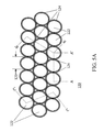
- FIG. 5A depicts a polycrystalline semiconductor containing nanoscale grains that have metallic elements lodged within the grain boundaries.
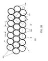
- FIG. 5B depicts a polycrystalline semiconductor containing nanoscale grains that have insulating compounds lodged within the grain boundaries.
- FIG. 6A depicts a two-dimensional (2-D) image of the energy band structure of a three-dimensional (3-D) quantum-dot semiconductor layer formed within a polycrystalline semiconductor matrix comprised of nanoscale grains that have metallic elements lodged within the grain boundaries.
- FIG. 6B depicts a two-dimensional (2-D) image of the energy band structure of a three-dimensional (3-D) quantum-dot semiconductor layer formed within a polycrystalline semiconductor matrix comprised of nanoscale grains that have insulating compounds lodged within the grain boundaries.
- FIG. 7 provides a cross-sectional view of a quantum dot field effect transistor.
- FIGS. 8 A, 8 B, 8 C are cross-sectional substrate views used to depict the method for making the semiconductor layer of a quantum well field effect transistor using a halogenated metalorganic precursor compound.
- FIG. 8D is a chemical diagram of a metalorganic precursor compound that can be used in association with FIGS. 8A-8C .
- FIG. 9 depicts an IGBT power FET that contains a nanoscale polycrystalline 3D electron gas layer.
- FIG. 10 depicts a semiconductor carrier comprising a quantum-dot opto-electronic or photonic device monolithically integrated onto its surface.
- FIG. 11 is a Table I showing Representative Grain—Grain Boundary Combinations for Insulating/Semi-insulating/Semiconducting Grain Boundaries for certain materials.
- FIG. 12 is a Table II showing Representative Grain—Grain Boundary Combinations for Insulating/Semi-insulating/Semiconducting Grain Boundaries for certain materials.
- the counterpart application de Rochemont '654 also instructs the insertion of tight-tolerance electroceramic material within the regions of localized reactive loading to increase or more precisely tune the coupling strength of localized reactive loads.
- the current application is also filed jointly with de Rochemont U.S. Ser. No. 13/216,692, entitled “POWER FET WITH RESONANT TRANSISTOR GATE”, filed Aug. 23, 2011 (de Rochemont '692), which is incorporated herein by reference.
- the co-pending application de Rochemont '692 instructs a power management module that modulates large currents at low current densities at pre-determined frequencies and methods to form the power management module on a semiconductor carrier.
- the '222 application instructs the monolithic integration of a low-loss power management circuit containing a surface FET.
- the '405 application discloses LCD methods to fabricate carbide, nitride and MAX-phase materials, such as silicon carbide, or complex chemistries that incorporate silicon and carbon elements.
- FIG. 3 depicts a semiconductor chip carrier 100 .
- the present invention may be applied to high-speed computing modules, RF radio modules, fully integrated radar modules, photonic modules, and opto-electronic modules. It may also apply to any circuit containing such a module or combination of the aforementioned modules that requires high power densities and high switching speed circuitry.
- the semiconductor chip carrier 100 contains a plurality of integrated circuits (semiconductor chips) 102 A, 102 B, 102 C, 102 D mounted either in discrete or stacked configuration on the carrier substrate 103 .
- the carrier substrate 103 is a larger semiconductor chip that has electrically conductive traces on its surface that are used to interconnect various components mounted or integrated thereupon. Additional low-level active circuitry, (not shown for clarity), may be embedded within the carrier substrate 103 . Such low-level active circuitry may include, but need not be limited to, latching, sensing, switching and signal drift circuitry useful in bus management systems. LCD processes may be used to integrate additional circuitry on the surface of the carrier substrate 103 , that may include, but need not be limited to, critical tolerance inductor coils 104 A, 104 B are used to form a tight tolerance LC circuit that stabilizes or actively tunes circuit clocking speeds, and/or passive networks 106 that are monolithically formed on the surface of the carrier substrate 103 .
- High-efficiency, high-speed fully integrated power management modules 108 are monolithically formed on the chip carrier 100 , using methods and embodiments detailed in the '042, '122, '159, '222, '654, '692, '922 applications incorporated herein by reference. These methods and embodiments may be used to optimize data transfer between memory devices and processor die, or other semiconductor die co-located on the semiconductor carrier 100 .
- FIGS. 4 - 8 A, 8 B, 8 C, 8 D describe how unique attributes of LCD manufacturing methods are applied to integrate semiconductor layers having thicknesses greater than 20-50 nm that are endowed with nanoscale microstructures necessary to generate three-dimensional (3D) electron gases within a semiconductor layer.
- LCD manufacturing methods allow dissimilar and “mismatched” materials with atomic-scale chemical uniformity and stoichiometric precision to be integrated in selected areas on the surface of semiconductor substrate with surface adhesion that is stronger than the tensile strength of the deposited material.
- LCD places no restriction on the number of elemental (chemical) components that can be incorporated with high compositional precision into the deposited material, which enables materials having high chemical complexity to be integrated into a monolithic structure.
- the low process temperatures ( ⁇ 400° C.) used by LCD do not alter dopant profiles of active components buried within the semiconductor substrate. These low deposition temperatures allow the LCD deposit to initially form as a uniform solid solution. This, in turn, provides means to form microstructures in LCD deposits that are restricted to nanoscale dimensions by the subsequent application of rapid thermal annealing processes.
- Uniform chemical distribution and nanoscale microstructures are a necessary condition to integrate electroceramic passive components having functional properties that remain stable with varying temperature, which satisfies critical performance tolerances needed to make the monolithic integration of passive circuitry within system-in-package (SiP) or a system-on-chip (SoC) economically viable.
- SiP system-in-package
- SoC system-on-chip
- FIG. 4 presents a table listing the charged carrier (electron-hole) mobilities of various semiconductors that can be used by the present invention. Higher switching speeds are enabled in semiconductor systems that have higher charged carrier mobility.
- FETs ultra-high speed field effect transistors
- These semiconductor materials typically have low effective electron mass, large ballistic mean free path and high saturation velocities.
- Preferred high carrier mobility semiconductor materials such as indium antimonide (InSb), typically have low band gap energies, which makes them prone to avalanche breakdown generated by impact ionization.
- V DS source-drain voltages
- FIGS. 1 & 2 instructs that runaway currents can be curtailed in low band gap semiconductors by forming a planar quantum well 28 by sandwiching the high carrier mobility/low band gap energy semiconductor as an ultra-thin layer 6 (20-50 nm thick) between layers 5 , 7 of a wider band gap semiconductor material, which in turn are sandwiched by layers 3 , 4 of an even wider band gap semiconductor.
- the narrow thickness of the ultra-thin layer 6 induces quantization effects within the quantum well 28 confined by energy band edges 26 , 27 . These quantization effects produce a 2D-electron gas having high electron mobility within the primary conduction channel defined by the quantum well 28 .
- the adjacent layers 5 , 7 comprising wider band gap semiconductor are selected to have conduction bands 21 , 22 that are close to the impact ionization threshold of the semiconductor material contained in the primary conduction channel 6 .
- This enables a secondary channel. Since the width of the secondary conduction channel 2 is greater than the dimensions needed to induce quantization effects, a 2D-electron gas is only created in the quantum well 28 of the primary conduction channel. This leads to a tradeoff that diminishes switching speeds, but mitigates avalanche currents by allowing some of the carriers that would otherwise reach impact ionization thresholds in the primary conduction channel 28 to be diverted to the secondary channel 2 , which has higher ionization thresholds.
- the prior art instructs that the semiconductor material used in the primary and secondary conduction channels in an ultra-high speed FET be formed using epitaxial methods to produce crystalline semiconductor that maximizes the carrier mobility, velocity and mean free path.
- FIGS. 5 A, 5 B, 6 A, 6 B show cross sections of three dimensional microscopic volumes of polycrystalline semiconductor material 120 that consists of matrix of semiconducting grains 122 that have a maximum physical dimension 123 less than 50 nm in diameter, preferably a maximum physical dimension 123 in the range of 20-50 nm.
- the polycrystalline material may comprise an elemental semiconductor, such as silicon or germanium, a IV-IV semiconductor, containing a plurality of elements from column IV of the periodic table, or consists of III-V semiconducting compounds, more preferably compositionally complex III-V semiconducting compounds.
- an elemental semiconductor such as silicon or germanium
- IV-IV semiconductor containing a plurality of elements from column IV of the periodic table
- III-V semiconducting compounds more preferably compositionally complex III-V semiconducting compounds.
- certain aspects of the present invention would favor the use of II-VI or IV-VI compound semiconductors, preferably compositionally complex II-VI or IV-VI compound semiconductors.
- polycrystalline semiconductors have greatly reduced charge carrier mobilities due to the reduced mean free paths caused by the lattice dislocations encountered as the charge carrier attempts to navigate the grain boundary.
- maximum physical dimensions 123 in the range 20-50 nm are small enough to form quantum wells that induce quantization effects as each grain 122 of the polycrystalline semiconductor material 120 becomes a quantum dot within the bulk material when a chemically distinct material envelops the grain 122 at the grain boundaries 124 , 126 .
- the quantum dot thereby produces a three-dimensional (3D) electron gas within each grain 122 .
- Quantum tunneling mechanisms represent the fastest charge transfer mechanism across an energy barrier, occurring at femtosecond time periods
- an additional preferred aspect of the present invention strengthens the energy barrier by optionally enveloping the semiconducting grains 122 with thin layers (2-10 nm thick, preferably 2-5 nm thick) of metallic grain boundary material 124 ( FIG. 5A ) or insulating grain boundary material 126 ( FIG. 5B ).
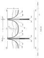
- the quantization effects induced by the phase-separated materials diffused into the grain boundaries are shown in FIGS. 6 A, 6 B.
- FIG. 6A depicts the energy band diagrams 130 of a 3D-electron gas, as viewed along any of the cross-sections A-A′, B-B′, C-C′ ( FIG. 5A ), that are established by the junctions created when 20-50 nm polycrystalline semiconducting grains 122 are enveloped by metallic grain boundary material 124 , which has a thickness ranging from 1 nm to 10 nm, but is preferably in the range of 2-4 nm.
- the metal-semiconductor interfaces 131 A, 131 B, 131 C, 131 D form junction barriers 132 A, 132 B, 132 C, 132 D through the equilibration of the Fermi level 133 in metallic grain boundaries 134 A, 134 B and the semiconducting grains 135 A, 135 B, 135 C.
- the equilibration process will cause electrons in the metallic grain boundaries and holes in the semiconducting grains to collect at the interface.
- the strong depletion fields in the semiconductor regions will cause the conduction bands 136 A, 136 B, 136 C to bend thereby producing energy wells 137 A, 137 B, 137 C that quantize the electron energy levels 138 in the conduction bands to form a 3D-electron gas.
- q is the electron charge
- ⁇ m is the metal work function
- ⁇ is the semiconductor electron affinity.
- Conduction electrons injected into and contained within the quantized energy levels 138 will tunnel through the junction barriers ( ⁇ B ) 132 A, 132 B, 132 C, 132 D at femtosecond transit speeds, which thereby makes very fast semiconductor switching speeds possible when these materials are configured in field effect transistor structures.
- the thin metallic grain boundary material 124 is a limitation in an FET-switched device as it will carry leakage currents that are undesirable in most applications. Therefore, it is preferable to form the polycrystalline semiconductor 121 that has electrically insulating or semi-insulating/semiconducting grain boundary material 126 enveloping the semiconductor grains 122 as depicted in FIG.
- FIG. 6B depicts the energy band diagrams 140 of a 3D-electron gas, as viewed along any of the cross-sections D-D′, E-E′, or F-F′ (see FIG. 5B ) that are established by the junctions created when 20-50 nm polycrystalline semiconducting grains 122 are enveloped by an insulating grain boundary material 126 , which has a thickness ranging from 1 nm to 10 nm, but is preferably in the range of 2-5 nm.
- the insulator may alternatively be a wider band gap semiconductor to produce a heterojunction between the grain 122 and the grain boundary 126 materials.
- the insulator-semiconductor interfaces 141 A, 141 B, 141 C, 141 D form junction barriers 142 A, 142 B through the equilibration of the Fermi level 143 in insulating grain boundaries 144 A, 144 B and the semiconducting grains 145 A, 145 B, 145 C.
- the offsets in the conduction band edges 146 A and valence band edges 146 B between in the semiconductor and insulator regions will create energy wells 147 A, 147 B, 147 C in the semiconductor grains 145 A, 145 B, 145 C that quantize the electron energy levels 148 in the conduction bands 149 to form a 3D-electron gas. Similar quantization occurs in the hole energy levels 150 in the valence bands 151 of the semiconductor grains 147 A, 147 B, 147 C. Since the semiconductor material is polycrystalline, the charge carriers have very short mean free paths (20-50 nm) and ballistic conduction currents never achieve the high velocities needed to generate impact ionization.
- tunneling currents having femtosecond transit times dominate conduction mechanisms between quantum wells in this polycrystalline semiconductor material.
- These transport processes enable fast switching speeds and reduce the risk of avalanche breakdown as ballistic electrons never form and the quantum energy wells distributed throughout the solid effectively shield atoms in the crystal lattice from the conducting electrons.
- a 3D electron (hole) gas is formed since the grains are roughly spherical and trap electrons in a three-dimensional quantum energy well through which the electrons may tunnel in all directions.
- thermodynamic and/or chemical incompatibility is required to phase separate the grain material from the grain boundary material while processing the polycrystalline grains.
- insulating, semi-insulating or semiconducting grain boundary materials 126 that consist primarily of elements found in a column of the periodic table that is separated by at least 2 or 3 columns from the elements comprising the nanoscale polycrystalline grains achieves this thermodynamic/chemical incompatibility.
- Table I lists representative combinations of group IV and III-V compound semiconductors (left hand side) that can be used within grains 122 that are enveloped by insulating, semi-insulating, or wide band gap II-VI and/or I-VII semiconductor materials located in the grain boundaries 126 .
- Table II lists representative combinations of low band gap II-VI compound semiconductors (left hand side) that can be used within grains 122 that are enveloped by insulating, semi-insulating, or wide band gap group VI semiconductor materials located in the grain boundaries 126 . Similar relationships with respect to column ranking apply when enveloping semiconducting grains 122 with conductive grain boundary materials 124 . Since LCD manufacturing methods enable the chemical integration of high chemical complexity materials, it should be clearly understood that III-V and II-VI semiconducting compounds need not be limited to binary compositions, but can easily comprise 3 or more elemental components.
- FIG. 7 depicts a significant aspect of the present invention, which provides means to construct a electrically active field, field effect transistor (FET) device 160 that can carry more substantial currents than the prior art.
- FET field effect transistor
- the primary conduction channel 161 may have polycrystalline semiconductor layer thickness ranging from 20 nm to 10 microns ( ⁇ m), preferably greater than 50 nm and most likely 1-2 ⁇ m, thereby allowing much higher currents to be modulated at significantly lower current densities.
- the conduction channel may optionally have additional layers 162 , 163 comprising a wider band gap semiconductor material inserted between it and the substrate 164 and/or the gate electrode 165 .
- Voltages applied to the gate electrode 165 are used to vary electric fields through the gate oxide 166 to modulate current flow in the primary conduction channel 161 between the source 167 and the drain 168 regions. Electrical contact is made to the source 167 and drain 168 regions using an ohmic source electrode 169 and drain electrode 170 , respectively.
- the high-speed quantum dot field effect transistor may be integrated in any circuit using LCD methods, apparatus, and processes, including, but not limited to, power management devices or silicon carriers that are used in high-speed computing processes or radio applications.
- FIGS. 8 A, 8 B, 8 C, 8 D describe how liquid chemical deposition (LCD) methods are used to form the polycrystalline 3D-electron gas semiconductor layers 161 .
- LCD liquid chemical deposition
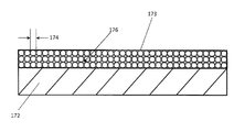
- de Rochemont et al, '112, and '159 describes describe the apparatus, and processes used by the LCD process to form an amorphous layer 171 on a substrate 172 .
- the substrate 172 may comprise an appropriately doped semiconductor wafer or a semiconductor layer.
- the amorphous layer 171 is formed on the substrate 172 by decomposing an aerosol spray of low volatility liquid metalorganic precursors consisting of a stoichiometric mixture of the desired semiconductor compound, its electronic dopants (if desired), and its grain boundary materials in an inert or reducing gas environments.
- the substrate 172 needs to be heated to a temperature that will pyrolyze liquid precursor compounds having the highest decomposition temperature, typically 200° C. to 500° C., preferably 300° C. to 400° C.
- the inert or reducing gas atmosphere may comprise nitrogen or noble gases, hydrogen, and/or reducing partial pressure ratios of carbon monoxide and carbon dioxide (by means of applying an aerosol spray of liquid metalorganic precursors to an appropriately doped semiconductor layer or wafer which functions as the substrate 172 ( FIG. 8A ).
- the amorphous layer may comprise an elemental semiconductor with electrical and other dopants, or it may be a compound semiconductor with electrical and other dopants.
- the LCD process enables the amorphous layer to have a precise ratio of chemical components that is compositionally uniform at the atomic scale. Spray deposition is followed by a bake out step that heats the substrate and deposit to temperatures between 400° C. and 600° C. for 2-20 minutes to remove any residual organic material that did not pyrolyze during the aerosol spray deposition step. The presence of any liquid species in the deposit will accelerate the deterioration of atomic scale chemical uniformity during subsequent annealing steps.
- a plasma annealing step is then used to render the amorphous layer 171 into a polycrystalline layer 173 that has uniform microstructure with grain sizes 174 ranging between 20-50 nm.
- Other thermal processing methods may be used to render the amorphous deposit into a polycrystalline state, but rapid thermal annealing process, and plasma annealing processes in particular, are preferred.
- the substrate 172 and deposit 171 may be pre-heated to temperatures in the range of 40° C. to 400° C. during the ionized plasma annealing step.
- Argon gas is the primary ballast used in the plasma annealing step, with additional gas additives consisting of nitrogen and/or carbon monoxide and carbon dioxide not exceeding 20% partial pressures.
- Total atmospheric pressures in the range of 1500 to 5000 mTorr, with power settings ranging from 50 W to 300 W for periods of 5 to 60 seconds are preferred for generating nanoscale polycrystalline semiconducting grains enveloped with a distinct phase grain boundary material.
- Halogenated metalorganic precursors to alkali metals, alkaline earth metals, or transition metals are added to the liquid precursor solution when it is desirable to form insulating grain boundaries 176 that comprise any of the I-VII grain boundary materials depicted in Tables I and II in the polycrystalline deposit 173 .
- Precursor molecules 177 essentially “carry” a metallic element 178 attached to an organic molecule that decomposes on the surface where the metallic element 178 is eventually deposited.
- Halogenated precursors will substitute one or more of the hydrogen elements 179 in the organic molecule with a halide element 180 from the group: fluorine, chlorine, iodine, or bromine.
- Halogenated alkali or alkaline earth metal precursors allows the elemental constituents of insulating compounds, comprising either a singular alkali or alkaline earth halide or a plurality of alkali or alkaline earth halides, to be transported to the deposition surface and integrated into the amorphous deposit and driven into the grain boundary regions 176 in a subsequent plasma annealing step.
- silicon carbide or aluminum nitride material phases can be introduced to the amorphous deposit 171 by forming a colloidal suspension of liquid metalorganic precursors and silicon carbide or aluminum nitride nanoparticles. These nanoparticle carbide and nitride phases will migrate to the grain boundaries during plasma annealing when their molar concentrations are held between 0.0001 mol % and 0.75 mol %.
- a specific advantage to the present invention is its ability to use the 3D electron gases generated by the nanoscale polycrystalline semiconductors to increase the carrier mobility within a specific layer or in a plurality of layers, which is not possible under the prior art.
- Low band gap semiconductors such as InSb can have very high charge carrier mobility, as shown in FIG.
- the 2D quantum wells create a quantized energy band structure within the planar low band gap semiconductor that effectively shields the valence band electrons from the conduction electrons travelling through the layer at ballistic velocities. Additional layers 3 , 4 of wider band gap semiconductor 24 , 25 can be added to further mitigate impact ionization processes.
- the 2D quantum wells shield valence band electrons and minimize electromagnetic interactions between the free electrons and the valence band electrons bound to the atoms forming the semiconductor material.
- the shielding reduces the conduction electron's effective mass, (“inertia”), which makes it more responsive to drift transport mechanisms under the influence of an applied electric field.
- tunneling processes represent the fastest electron transport mechanism. Tunneling processes are possible between adjacent quantum wells (not shown), but not within a low band gap semiconductor layer since there are no energy barriers within layer forming the bottom of the well. (Adjacent quantum wells can be visualized by imagining a plurality of multilayer structures in the vertical direction of FIG. 1 .)
- the principal benefits to a planar 2D electron gas is a lowered electron (and hole) effective mass and reduced susceptibility to impact ionization within a very thin (20-50 nm) layer of a low-band gap semiconductor layer.
- the 3D quantum wells of the present invention interject an energy barrier at the boundary of every grain. Therefore, the mean free path of any conduction electron is limited to the nanoscale dimension of the grain (20 nm to 50 nm). The drifting electron will then encounter a thin (2 nm to 10 nm) energy barrier through which it will tunnel.
- the combination of reduced mean free path (reduced impact ionization) and tunneling currents in the direction or primary drift currents allows all types of semiconductor materials to support fast transport processes in any direction, without the restriction of limiting the modulated current to a 20-50 nm layer.
- any of the layers 161 , 162 , 163 , 164 may be formed as an arbitrarily thick semiconducting 3D electron gas.
- each individual layer 161 , 162 , 163 , 164 may be composed of semiconducting grains having an energy band gap that is distinct from the band gap in a neighboring polycrystalline semiconducting layer.
- This aspect of the invention is particularly beneficial to device structures where switching speeds are limited by reduced carrier mobility in bulk semiconducting layers by virtue of the layer's electronic doping, as is the case with the insulated gate bipolar transistor (IGBT) where the p + -doping layer will limit switching speeds.
- FIG. 9 depicts a cross-sectional view of an IGBT device 200 integrated on the silicon chip carrier, which may optionally include the semiconductor carrier substrate 202 and electrode 204 that functions as a ground and a heat sink.
- LCD enables the insertion of a very thin amorphous layer 206 that allows a single crystal p + -type semiconductor drain layer comprising a semiconducting 3D electron gas layer 208 to be deposited upon the drain electrode 204 , which may also comprise a 3D electron gas layer.
- a p-n junction 210 forms between the p + -type semiconductor drain layer 208 and an n ⁇ -type semiconductor layer 212 that may optionally consist of 3D electron gas polycrystalline material.
- the n ⁇ -type semiconductor layer is electrically patterned with p-type subchannel 214 A, 214 B, 214 C and n+-type dopant profiles 216 A, 216 B, 216 C, 216 D that are in electrical communication with the source electrode 218 .
- the insulated gate electrode 220 modulates inversion carrier populations in a channel 222 that allow currents to flow from the drain 208 to the source electrode 218 .
- the gate electrode 220 is encapsulated within a low loss high-dielectric breakdown insulating material 224 A, 224 B, preferably an amorphous silica insulating material. Any or all of the semiconductor layers may consist of a nanoscale engineered polycrystalline semiconductor modified to generate a 3D electron gas.
- each of the 3D electron gas semiconductor regions 226 A, 226 B, 228 A, 228 B may comprise polycrystalline grains having energy band gaps that differ from the energy band gaps in any of the adjacent semiconductor material in the IGBT device 200 , thus forming a plurality of heterostructures within the three-dimensionally pattered monolithic structure.
- FIG. 10 depicts a semiconducting carrier 250 that consists of a power management module 252 monolithically integrated upon the surface of the carrier substrate 254 , one or more semiconductor die 256 mounted thereupon, and an opto-electronic or photonic device 258 that contains a 3D electron gas semiconducting layer 260 embedded within it.
- quantum well technology and manufacturing methods described herein may be easily applied to any other form of quantum well devices, including but not limited to multiplexers, signal encoders, and sensors. It is further readily understood that the devices described above embody methods of manufacture and methods of operation which are also new and non-obvious with respect to the prior art.
Landscapes
- Engineering & Computer Science (AREA)
- Chemical & Material Sciences (AREA)
- Nanotechnology (AREA)
- Crystallography & Structural Chemistry (AREA)
- Physics & Mathematics (AREA)
- Mathematical Physics (AREA)
- Theoretical Computer Science (AREA)
- General Physics & Mathematics (AREA)
- Condensed Matter Physics & Semiconductors (AREA)
- Manufacturing & Machinery (AREA)
- Thin Film Transistor (AREA)
- Liquid Deposition Of Substances Of Which Semiconductor Devices Are Composed (AREA)
- Insulated Gate Type Field-Effect Transistor (AREA)
- Junction Field-Effect Transistors (AREA)
- Semiconductor Lasers (AREA)
- Recrystallisation Techniques (AREA)
Abstract
Description
qφ B =q(φm−χ) (1)
Claims (16)
Priority Applications (3)
| Application Number | Priority Date | Filing Date | Title |
|---|---|---|---|
| US13/288,922 US9123768B2 (en) | 2010-11-03 | 2011-11-03 | Semiconductor chip carriers with monolithically integrated quantum dot devices and method of manufacture thereof |
| US14/839,364 US20150372091A1 (en) | 2010-11-03 | 2015-08-28 | Semiconductor chip carriers with monolithically integrated quantum dot devices and method of manufacture thereof |
| US15/496,962 US10777409B2 (en) | 2010-11-03 | 2017-04-25 | Semiconductor chip carriers with monolithically integrated quantum dot devices and method of manufacture thereof |
Applications Claiming Priority (2)
| Application Number | Priority Date | Filing Date | Title |
|---|---|---|---|
| US40984610P | 2010-11-03 | 2010-11-03 | |
| US13/288,922 US9123768B2 (en) | 2010-11-03 | 2011-11-03 | Semiconductor chip carriers with monolithically integrated quantum dot devices and method of manufacture thereof |
Related Child Applications (1)
| Application Number | Title | Priority Date | Filing Date |
|---|---|---|---|
| US14/839,364 Continuation US20150372091A1 (en) | 2010-11-03 | 2015-08-28 | Semiconductor chip carriers with monolithically integrated quantum dot devices and method of manufacture thereof |
Publications (2)
| Publication Number | Publication Date |
|---|---|
| US20120104358A1 US20120104358A1 (en) | 2012-05-03 |
| US9123768B2 true US9123768B2 (en) | 2015-09-01 |
Family
ID=45995653
Family Applications (3)
| Application Number | Title | Priority Date | Filing Date |
|---|---|---|---|
| US13/288,922 Active 2032-08-01 US9123768B2 (en) | 2010-11-03 | 2011-11-03 | Semiconductor chip carriers with monolithically integrated quantum dot devices and method of manufacture thereof |
| US14/839,364 Abandoned US20150372091A1 (en) | 2010-11-03 | 2015-08-28 | Semiconductor chip carriers with monolithically integrated quantum dot devices and method of manufacture thereof |
| US15/496,962 Active 2032-04-21 US10777409B2 (en) | 2010-11-03 | 2017-04-25 | Semiconductor chip carriers with monolithically integrated quantum dot devices and method of manufacture thereof |
Family Applications After (2)
| Application Number | Title | Priority Date | Filing Date |
|---|---|---|---|
| US14/839,364 Abandoned US20150372091A1 (en) | 2010-11-03 | 2015-08-28 | Semiconductor chip carriers with monolithically integrated quantum dot devices and method of manufacture thereof |
| US15/496,962 Active 2032-04-21 US10777409B2 (en) | 2010-11-03 | 2017-04-25 | Semiconductor chip carriers with monolithically integrated quantum dot devices and method of manufacture thereof |
Country Status (5)
| Country | Link |
|---|---|
| US (3) | US9123768B2 (en) |
| EP (1) | EP2636069B1 (en) |
| JP (2) | JP6223828B2 (en) |
| CN (1) | CN103415925A (en) |
| WO (1) | WO2012061656A2 (en) |
Cited By (3)
| Publication number | Priority date | Publication date | Assignee | Title |
|---|---|---|---|---|
| US9348385B2 (en) | 2012-07-09 | 2016-05-24 | L. Pierre deRochement | Hybrid computing module |
| US20160225759A1 (en) * | 2010-08-23 | 2016-08-04 | L. Pierre de Rochemont | Power fet with a resonant transistor gate |
| WO2019236734A1 (en) | 2018-06-05 | 2019-12-12 | De Rochemont L Pierre | Module with high peak bandwidth i/o channels |
Families Citing this family (8)
| Publication number | Priority date | Publication date | Assignee | Title |
|---|---|---|---|---|
| US20140116491A1 (en) * | 2012-10-29 | 2014-05-01 | Alphabet Energy, Inc. | Bulk-size nanostructured materials and methods for making the same by sintering nanowires |
| US9614112B2 (en) | 2013-09-11 | 2017-04-04 | The University Of Connecticut | Imaging cell array integrated circuit |
| WO2017091269A2 (en) * | 2015-08-31 | 2017-06-01 | The Board Of Regents Of The University Of Oklahoma | Semiconductor devices having matrix-embedded nano-structured materials |
| US11313040B2 (en) * | 2017-03-24 | 2022-04-26 | Embraco Indústria De Compressores E Soluçôes Em Refrigeraçâo Ltda. | Plasma-assisted process of ceramization of polymer precursor on surface, surface comprising ceramic polymer |
| KR102196005B1 (en) | 2017-10-18 | 2020-12-30 | 한양대학교 산학협력단 | Layer and Multilevel Element |
| WO2020261471A1 (en) * | 2019-06-27 | 2020-12-30 | 日本電信電話株式会社 | Tunnel field-effect transistor and method for manufacturing same |
| US12310129B2 (en) * | 2020-05-21 | 2025-05-20 | Faquir Chand Jain | Quantum dot channel (QDC) quantum dot gate transistors, memories and other devices |
| US20260047151A1 (en) * | 2024-08-06 | 2026-02-12 | POSTECH Research and Business Development Foundation | Device of removing low frequency noise |
Citations (160)
| Publication number | Priority date | Publication date | Assignee | Title |
|---|---|---|---|---|
| US2283925A (en) | 1937-04-30 | 1942-05-26 | Rca Corp | High frequency core and shield and method of making the same |
| US2886529A (en) | 1952-07-31 | 1959-05-12 | Centre Nat Rech Scient | Magnetic materials and their methods of manufacture |
| GB1125897A (en) | 1965-06-18 | 1968-09-05 | Westinghouse Electric Corp | Frequency selective electronic apparatus |
| US3574114A (en) | 1968-08-05 | 1971-04-06 | Bell Telephone Labor Inc | Fine grain ceramic ferrites |
| US3614554A (en) | 1968-10-24 | 1971-10-19 | Texas Instruments Inc | Miniaturized thin film inductors for use in integrated circuits |
| US3983077A (en) | 1975-05-02 | 1976-09-28 | Texas Instruments Incorporated | Process for making ceramic resistor materials |
| EP0026056A1 (en) | 1979-09-04 | 1981-04-01 | Western Electric Company, Incorporated | Semiconductor integrated circuit protection arrangement |
| US4400683A (en) | 1981-09-18 | 1983-08-23 | Matsushita Electric Industrial Co., Ltd. | Voltage-dependent resistor |
| US4455545A (en) | 1982-11-05 | 1984-06-19 | Sperry Corporation | High frequency output inductor for inverter power supply |
| US4523170A (en) | 1982-11-05 | 1985-06-11 | Spang & Company | Adjustable air gap ferrite structures and methods of manufacture |
| US4646038A (en) | 1986-04-07 | 1987-02-24 | Motorola, Inc. | Ceramic resonator filter with electromagnetic shielding |
| US4759120A (en) | 1986-05-30 | 1988-07-26 | Bel Fuse Inc. | Method for surface mounting a coil |
| US4859492A (en) | 1986-02-24 | 1989-08-22 | Hughes Aircraft Company | Process for forming an environmentally stable optical coating thereby |
| US4880770A (en) | 1987-05-04 | 1989-11-14 | Eastman Kodak Company | Metalorganic deposition process for preparing superconducting oxide films |
| US4967201A (en) | 1987-10-22 | 1990-10-30 | Westinghouse Electric Corp. | Multi-layer single substrate microwave transmit/receive module |
| US5084749A (en) | 1988-08-25 | 1992-01-28 | Eastman Kodak Company | Image sensing device with reduced smear |
| US5130675A (en) | 1990-09-10 | 1992-07-14 | Fujitsu Limited | Voltage-controlled oscillator |
| US5139999A (en) | 1990-03-08 | 1992-08-18 | President And Fellows Of Harvard College | Chemical vapor deposition process where an alkaline earth metal organic precursor material is volatilized in the presence of an amine or ammonia and deposited onto a substrate |
| US5154973A (en) | 1989-12-07 | 1992-10-13 | Murata Manufacturing Co., Ltd. | Composite material for dielectric lens antennas |
| US5198824A (en) | 1992-01-17 | 1993-03-30 | Texas Instruments Incorporated | High temperature co-fired ceramic integrated phased array packaging |
| US5217754A (en) | 1987-07-27 | 1993-06-08 | Trustees Of The University Of Pennsylvania | Organometallic precursors in conjunction with rapid thermal annealing for synthesis of thin film ceramics |
| US5219377A (en) | 1992-01-17 | 1993-06-15 | Texas Instruments Incorporated | High temperature co-fired ceramic integrated phased array package |
| US5263198A (en) | 1991-11-05 | 1993-11-16 | Honeywell Inc. | Resonant loop resistive FET mixer |
| US5272485A (en) | 1992-02-04 | 1993-12-21 | Trimble Navigation Limited | Microstrip antenna with integral low-noise amplifier for use in global positioning system (GPS) receivers |
| US5403797A (en) | 1993-01-21 | 1995-04-04 | Tdk Corporation | Non-reducing dielectric ceramic composition |
| US5427988A (en) | 1993-06-09 | 1995-06-27 | The United States Of America As Represented By The Secretary Of The Army | Ceramic ferroelectric composite material - BSTO-MgO |
| US5456945A (en) | 1988-12-27 | 1995-10-10 | Symetrix Corporation | Method and apparatus for material deposition |
| US5478610A (en) | 1994-09-02 | 1995-12-26 | Ceram Incorporated | Metalorganic chemical vapor deposition of layered structure oxides |
| US5513382A (en) | 1993-03-31 | 1996-04-30 | Motorola, Inc. | Multi-ceramic layer switch circuit |
| US5535445A (en) | 1983-05-09 | 1996-07-09 | The Secretary Of State For Defence In Her Britannic Majesty's Government Of The United Kingdom Of Great Britain And Northern Ireland | Mixer circuit |
| US5543773A (en) | 1990-09-07 | 1996-08-06 | Electrotech Instruments Limited | Transformers and coupled inductors with optimum interleaving of windings |
| US5584053A (en) | 1995-08-04 | 1996-12-10 | Motorola, Inc. | Commonly coupled high frequency transmitting/receiving switching module |
| US5590387A (en) | 1993-10-27 | 1996-12-31 | H. C. Starck, Gmbh & Co, Kg | Method for producing metal and ceramic sintered bodies and coatings |
| US5614252A (en) | 1988-12-27 | 1997-03-25 | Symetrix Corporation | Method of fabricating barium strontium titanate |
| US5625365A (en) | 1995-03-10 | 1997-04-29 | Trimble Navigation Limited | Dual-frequency microwave radio antenna system |
| US5635433A (en) | 1995-09-11 | 1997-06-03 | The United States Of America As Represented By The Secretary Of The Army | Ceramic ferroelectric composite material-BSTO-ZnO |
| US5707459A (en) | 1993-06-24 | 1998-01-13 | Canon Kabushiki Kaisha | Solar cell module provided with a heat-fused portion |
| US5707715A (en) | 1996-08-29 | 1998-01-13 | L. Pierre deRochemont | Metal ceramic composites with improved interfacial properties and methods to make such composites |
| US5747870A (en) | 1994-06-30 | 1998-05-05 | Plessey Semiconductors Limited | Multi-chip module inductor structure |
| US5759923A (en) | 1991-02-25 | 1998-06-02 | Symetrix Corporation | Method and apparatus for fabricating silicon dioxide and silicon glass layers in integrated circuits |
| US5764189A (en) | 1995-09-27 | 1998-06-09 | Siemens Aktiengesellschaft | Doppler radar module |
| US5771567A (en) | 1996-08-29 | 1998-06-30 | Raytheon Company | Methods of fabricating continuous transverse stub radiating structures and antennas |
| US5854608A (en) | 1994-08-25 | 1998-12-29 | Symetri Com, Inc. | Helical antenna having a solid dielectric core |
| US5859621A (en) | 1996-02-23 | 1999-01-12 | Symmetricom, Inc. | Antenna |
| US5889459A (en) | 1995-03-28 | 1999-03-30 | Matsushita Electric Industrial Co., Ltd. | Metal oxide film resistor |
| US5892489A (en) | 1996-04-05 | 1999-04-06 | Murata Manufacturing Co., Ltd. | Chip antenna and method of making same |
| US5903421A (en) | 1996-10-21 | 1999-05-11 | Murata Manufacturing Co., Ltd. | High-frequency composite part |
| US5933121A (en) | 1998-04-07 | 1999-08-03 | Harris Corporation | Antenna array for sensing signals on conductors |
| US5945963A (en) | 1996-01-23 | 1999-08-31 | Symmetricom, Inc. | Dielectrically loaded antenna and a handheld radio communication unit including such an antenna |
| EP0939451A1 (en) | 1998-02-27 | 1999-09-01 | Kyocera Corporation | Slot antenna |
| US6023251A (en) | 1998-06-12 | 2000-02-08 | Korea Electronics Technology Institute | Ceramic chip antenna |
| US6027826A (en) | 1994-06-16 | 2000-02-22 | The United States Of America As Represented By The Secretary Of The Air Force | Method for making ceramic-metal composites and the resulting composites |
| US6028568A (en) | 1997-12-11 | 2000-02-22 | Murata Manufacturing Co., Ltd. | Chip-antenna |
| US6031445A (en) | 1997-11-28 | 2000-02-29 | Stmicroelectronics S.A. | Transformer for integrated circuits |
| US6040805A (en) | 1998-05-08 | 2000-03-21 | Antcom Corp. | Low profile ceramic choke |
| US6046707A (en) | 1997-07-02 | 2000-04-04 | Kyocera America, Inc. | Ceramic multilayer helical antenna for portable radio or microwave communication apparatus |
| US6052040A (en) | 1997-03-03 | 2000-04-18 | Ngk Spark Plug Co., Ltd. | Dielectric duplexer with different capacitive coupling between antenna pad and transmitting and receiving sections |
| US6111544A (en) | 1998-02-13 | 2000-08-29 | Murata Manufacturing Co., Ltd. | Chip antenna, antenna device, and mobile communication apparatus |
| US6130471A (en) * | 1997-08-29 | 2000-10-10 | The Whitaker Corporation | Ballasting of high power silicon-germanium heterojunction biploar transistors |
| US6143432A (en) | 1998-01-09 | 2000-11-07 | L. Pierre deRochemont | Ceramic composites with improved interfacial properties and methods to make such composites |
| US6154176A (en) | 1998-08-07 | 2000-11-28 | Sarnoff Corporation | Antennas formed using multilayer ceramic substrates |
| US6195049B1 (en) | 1998-09-11 | 2001-02-27 | Samsung Electronics Co., Ltd. | Micro-strip patch antenna for transceiver |
| US6204203B1 (en) | 1998-10-14 | 2001-03-20 | Applied Materials, Inc. | Post deposition treatment of dielectric films for interface control |
| US6208843B1 (en) | 1999-06-03 | 2001-03-27 | Cirocomm Technology Corp. | Radio frequency and microwave module for simultaneously transmitting data and audio signal |
| US6222489B1 (en) | 1995-08-07 | 2001-04-24 | Murata Manufacturing Co., Ltd. | Antenna device |
| US6266020B1 (en) | 2000-07-24 | 2001-07-24 | Auden Technology Mfg. Co. Ltd. | Hidden antenna device of a mobile phone |
| US6271803B1 (en) | 1998-07-03 | 2001-08-07 | Murata Manufacturing Co., Ltd. | Chip antenna and radio equipment including the same |
| US20010023779A1 (en) | 2000-02-09 | 2001-09-27 | Yasuhiro Sugaya | Transfer material, method for producing the same and wiring substrate produced by using the same |
| US20010027119A1 (en) | 2000-03-23 | 2001-10-04 | Murata Manufacturing Co., Ltd. Nagaokakyo-Shi, Japan | Mobile communication device and high-frequency composite unit used in the same |
| US6300894B1 (en) | 1999-07-09 | 2001-10-09 | Harris Corporation | Antenna having electrically controllable radar cross-section |
| US6323549B1 (en) | 1996-08-29 | 2001-11-27 | L. Pierre deRochemont | Ceramic composite wiring structures for semiconductor devices and method of manufacture |
| US20010048969A1 (en) | 1997-05-05 | 2001-12-06 | Constantino Stephen A. | Dispersible, metal oxide-coated, barium titanate materials |
| US20020039667A1 (en) | 2000-04-27 | 2002-04-04 | Tdk Corporation | Composite magnetic material and magnetic molding material, magnetic powder compression molding material, and magnetic paint using the composite magnetic material, composite dielectric material and molding material, powder compression molding material, paint, prepreg, and substrate using the composite dielectric material, and electronic part |
| US20020047768A1 (en) | 2000-10-10 | 2002-04-25 | Duffy Thomas P. | Microelectronic magnetic structure, device including the structure, and methods of forming the structure and device |
| US20020070983A1 (en) | 2000-12-07 | 2002-06-13 | Kozub Thomas A. | Automated wafer handling with graphic user interface |
| US20020092472A1 (en) | 1999-02-03 | 2002-07-18 | Symetrix Corporation And Matsushita Electronics Corporation | Method of liquid deposition by selection of liquid viscosity and other precursor properties |
| US20020110004A1 (en) | 1994-10-31 | 2002-08-15 | Parks David B. | Resonant gate driver |
| US6492949B1 (en) | 2000-08-16 | 2002-12-10 | Raytheon Company | Slot antenna element for an array antenna |
| US6496149B1 (en) | 2001-02-01 | 2002-12-17 | Apple Computer, Inc. | Recessed aperture-coupled patch antenna with multiple dielectrics for wireless applications |
| US20020190818A1 (en) | 2000-09-25 | 2002-12-19 | Kenji Endou | High frequency band pass filter |
| US6501415B1 (en) | 2000-08-16 | 2002-12-31 | Raytheon Company | Highly integrated single substrate MMW multi-beam sensor |
| US20030002045A1 (en) | 2001-05-23 | 2003-01-02 | The Regents Of The University Of California | Composite material having low electromagnetic reflection and refraction |
| US20030034124A1 (en) | 2001-06-19 | 2003-02-20 | Yasuhiro Sugaya | Dielectric resonator, dielectric filter and method of producing the same, filter device combined to a transmit-receive antenna and communication apparatus using the same |
| US6541820B1 (en) | 2000-03-28 | 2003-04-01 | International Rectifier Corporation | Low voltage planar power MOSFET with serpentine gate pattern |
| US20030073565A1 (en) | 2001-06-01 | 2003-04-17 | Ellis Marion E. | Tunable dielectric compositions including low loss glass |
| US6552693B1 (en) | 1998-12-29 | 2003-04-22 | Sarantel Limited | Antenna |
| US20030080325A1 (en) | 2001-10-26 | 2003-05-01 | Symetrix Corporation And Matsushita Electric Industrial Co., Ltd. | Chemical vapor deposition method of making layered superlattice materials using trimethylbismuth |
| US6559735B1 (en) | 2000-10-31 | 2003-05-06 | Cts Corporation | Duplexer filter with an alternative signal path |
| US20030107455A1 (en) | 2001-10-23 | 2003-06-12 | Yoshihiko Imanaka | Integrated ceramic module and microwave dielectric composition |
| US20030111714A1 (en) | 2001-12-03 | 2003-06-19 | Dover Capital Formation Group | Surface mount ceramic package |
| US6583699B2 (en) | 2000-10-31 | 2003-06-24 | Tdk Corporation | Magnetic material and inductor |
| US20030122647A1 (en) | 2001-12-28 | 2003-07-03 | Chiung-Ting Ou | Inductor formed on a silicon substrate and method of manufacturing the same |
| US20030148024A1 (en) | 2001-10-05 | 2003-08-07 | Kodas Toivo T. | Low viscosity precursor compositons and methods for the depositon of conductive electronic features |
| US6605151B1 (en) | 1999-11-29 | 2003-08-12 | Northwestern University | Oxide thin films and composites and related methods of deposition |
| US6611419B1 (en) | 2000-07-31 | 2003-08-26 | Intel Corporation | Electronic assembly comprising substrate with embedded capacitors |
| US20030161959A1 (en) | 2001-11-02 | 2003-08-28 | Kodas Toivo T. | Precursor compositions for the deposition of passive electronic features |
| US20030170436A1 (en) | 2001-12-25 | 2003-09-11 | Ngk Spark Plug Co., Ltd. | Dielectric material and dielectric sintered body, and wiring board using the same |
| US6620750B2 (en) | 2001-05-18 | 2003-09-16 | Kook-Sun Hong | Dielectric ceramic composition and method for manufacturing multilayered components using the same |
| CN1450580A (en) | 2003-04-10 | 2003-10-22 | 复旦大学 | Field emission nano material capable of being used in plane display |
| US6639556B2 (en) | 2000-10-10 | 2003-10-28 | Alps Electric Co., Ltd. | Plane patch antenna through which desired resonance frequency can be obtained with stability |
| US6650303B2 (en) | 2001-06-15 | 2003-11-18 | Korea Institute Of Science And Technology | Ceramic chip antenna |
| US20030221621A1 (en) | 2000-04-21 | 2003-12-04 | Applied Materials Inc. | Method and apparatus for processing semiconductor substrates with hydroxyl radicals |
| US6670497B2 (en) | 2000-04-24 | 2003-12-30 | Toho Titanium Co., Ltd. | Phthalic diester derivatives and electron donors |
| US20040001028A1 (en) | 2002-06-27 | 2004-01-01 | Killen William D. | System for improved matching and broadband performance of microwave antennas |
| US20040001027A1 (en) | 2002-06-27 | 2004-01-01 | Killen William D. | Dipole arrangements using dielectric substrates of meta-materials |
| US20040000970A1 (en) | 2002-06-27 | 2004-01-01 | Killen William D. | High efficiency coupled line filters |
| US20040001024A1 (en) | 2002-06-27 | 2004-01-01 | Killen William D. | High efficiency printed circuit array of log-periodic dipole arrays |
| US20040001026A1 (en) | 2002-06-27 | 2004-01-01 | Killen William D. | High efficiency antennas of reduced size on dielectric substrate |
| US20040000975A1 (en) | 2002-06-27 | 2004-01-01 | Killen William D. | High efficiency single port resonant line |
| US20040000976A1 (en) | 2002-06-27 | 2004-01-01 | Killen William D. | High efficiency resonant line |
| US20040000964A1 (en) | 2002-06-27 | 2004-01-01 | Killen William D. | High efficiency directional coupler |
| US20040000972A1 (en) | 2002-06-27 | 2004-01-01 | Killen William D. | High efficiency interdigital filters |
| US20040000966A1 (en) | 2002-06-27 | 2004-01-01 | Killen William D. | High efficiency four port circuit |
| US6680700B2 (en) | 2000-10-09 | 2004-01-20 | Koninklijke Philips Electronics N.V. | Miniaturized microwave antenna |
| US20040012081A1 (en) | 2002-07-19 | 2004-01-22 | Kwon Heung Kyu | Semiconductor wafer having electrically connected passive device chips, passive devices and semiconductor package using the same |
| US6683576B2 (en) | 2001-09-04 | 2004-01-27 | Koninklijke Philips Electronics N.V. | Circuit board and SMD antenna |
| US6686406B2 (en) | 2000-04-26 | 2004-02-03 | The Furukawa Electric Co., Ltd. | Dielectric ceramic, resin-ceramic composite material, electrical part and antenna, and manufacturing method thereof |
| US6690336B1 (en) | 1998-06-16 | 2004-02-10 | Symmetricom, Inc. | Antenna |
| US20040033654A1 (en) | 2002-08-14 | 2004-02-19 | Osamu Yamagata | Semiconductor device and method of fabricating the same |
| US6697605B1 (en) | 1999-06-09 | 2004-02-24 | Murata Manufacturing Co. Ltd. | High-frequency circuit apparatus and communication apparatus |
| US20040070915A1 (en) | 2001-09-06 | 2004-04-15 | Atsushi Nagai | Ceramic electronic component and production method therefor |
| US20040070334A1 (en) * | 2001-02-28 | 2004-04-15 | Buckley Alastair Robert | Encapsulated electrode |
| US20040084080A1 (en) | 2002-06-22 | 2004-05-06 | Nanosolar, Inc. | Optoelectronic device and fabrication method |
| US20040092236A1 (en) | 2002-11-08 | 2004-05-13 | Kiyoshi Irie | Semiconductor integrated circuit device and wireless communication system |
| US6743744B1 (en) | 2000-05-03 | 2004-06-01 | Korea Institute Of Science And Technology | Low temperature sinterable and low loss dielectric ceramic compositions and method thereof |
| US20040113738A1 (en) | 2000-03-10 | 2004-06-17 | Ahn Kie Y | Integrated circuit inductor with a magnetic core |
| US20040118448A1 (en) | 2002-09-05 | 2004-06-24 | Nanosys, Inc. | Nanostructure and nanocomposite based compositions and photovoltaic devices |
| US6762237B2 (en) | 2001-06-08 | 2004-07-13 | Eikos, Inc. | Nanocomposite dielectrics |
| US20040145874A1 (en) * | 2003-01-23 | 2004-07-29 | Stephane Pinel | Method, system, and apparatus for embedding circuits |
| US6791496B1 (en) | 2003-03-31 | 2004-09-14 | Harris Corporation | High efficiency slot fed microstrip antenna having an improved stub |
| US20040189528A1 (en) | 2003-03-31 | 2004-09-30 | Killen William D. | Arangements of microstrip antennas having dielectric substrates including meta-materials |
| US20040195575A1 (en) * | 2002-03-08 | 2004-10-07 | Takuya Komoda | Quantum device |
| US20050036269A1 (en) | 2001-09-07 | 2005-02-17 | Intel Corporation | Vacuum-cavity MEMS resonator |
| US6864848B2 (en) | 2001-12-27 | 2005-03-08 | Hrl Laboratories, Llc | RF MEMs-tuned slot antenna and a method of making same |
| US20050051870A1 (en) | 2002-12-27 | 2005-03-10 | Semiconductor Energy Laboratory Co., Ltd. | Semiconductor device and a method of manufacturing the same |
| US6906674B2 (en) | 2001-06-15 | 2005-06-14 | E-Tenna Corporation | Aperture antenna having a high-impedance backing |
| US20050127389A1 (en) * | 2003-12-04 | 2005-06-16 | Hiroyuki Fujiwara | Semiconductor apparatus, LED print head, and printer |
| US6919119B2 (en) | 2000-05-30 | 2005-07-19 | The Penn State Research Foundation | Electronic and opto-electronic devices fabricated from nanostructured high surface to volume ratio thin films |
| US20060086994A1 (en) | 2004-05-14 | 2006-04-27 | Susanne Viefers | Nanoelectromechanical components |
| US20060092079A1 (en) | 2004-10-01 | 2006-05-04 | De Rochemont L P | Ceramic antenna module and methods of manufacture thereof |
| US20060125681A1 (en) | 2002-08-29 | 2006-06-15 | The Regents Of The University Of California | Indefinite materials |
| US20060134491A1 (en) | 2003-06-10 | 2006-06-22 | Hilchenko Galina V | Zirconium dioxide-based electrode-electrolyte pair (variants), method for the production thereof (variants) and organogel |
| US20060189104A1 (en) * | 2005-02-24 | 2006-08-24 | Hon Hai Precision Industry Co., Ltd. | Method for forming a quantum dot pattern |
| US20070003781A1 (en) | 2005-06-30 | 2007-01-04 | De Rochemont L P | Electrical components and method of manufacture |
| US20070137257A1 (en) | 2005-12-16 | 2007-06-21 | Desantolo Anthony Michael | Apparatus and method for fabricating glass bodies using an aerosol delivery system |
| US20070139976A1 (en) | 2005-06-30 | 2007-06-21 | Derochemont L P | Power management module and method of manufacture |
| US20070166453A1 (en) | 2004-02-19 | 2007-07-19 | Nanosolar, Inc. | High-throughput printing of chalcogen layer |
| US20070170535A1 (en) | 2006-01-24 | 2007-07-26 | De Rochemont L Pierre | Photovoltaic devices with silicon dioxide encapsulation layer and method to make same |
| US20070181906A1 (en) | 2005-12-28 | 2007-08-09 | George Chik | Carbon passivation in solid-state light emitters |
| US20070259768A1 (en) | 2006-05-03 | 2007-11-08 | Kear Bernard H | Nanocomposite ceramic and method for producing the same |
| US20080136395A1 (en) | 2006-11-20 | 2008-06-12 | Bennett Paul T | Methods and apparatus for a spread spectrum switching regulator |
| US20090004370A1 (en) | 2007-05-30 | 2009-01-01 | Fabio Zurcher | Metal Inks, Methods of Making the Same, and Methods for Printing and/or Forming Metal Films |
| US20090015314A1 (en) | 2001-12-15 | 2009-01-15 | Huettinger Elektronik Gmbh + Co. Kg | High frequency excitation system |
| US7564887B2 (en) | 2004-06-30 | 2009-07-21 | Finisar Corporation | Long wavelength vertical cavity surface emitting lasers |
| US20100108986A1 (en) | 2006-12-16 | 2010-05-06 | Helmholtz-Zentrum Berlin Fuer Materialien Und Energie Gmbh | Method for the production of quantum dots embedded in a matrix, and quantum dots embedded in a matrix produced using the method |
| US20100155786A1 (en) * | 2004-06-08 | 2010-06-24 | Nanosys, Inc. | Methods and devices for forming nanostructure monolayers and devices including such monolayers |
| US20110021007A1 (en) | 2006-01-24 | 2011-01-27 | De Rochemont L Pierre | Liquid chemical depostion apparatus and process and products therefrom |
| US20110049394A1 (en) | 2009-09-01 | 2011-03-03 | De Rochemont L Pierre | Ionizing disinfectant surface |
| US20110065224A1 (en) | 2007-12-06 | 2011-03-17 | Brent Bollman | Methods and devices for processing a precursor layer in a group via environment |
| US20110248900A1 (en) | 2009-06-17 | 2011-10-13 | De Rochemont L Pierre | Frequency-selective dipole antennas |
Family Cites Families (31)
| Publication number | Priority date | Publication date | Assignee | Title |
|---|---|---|---|---|
| US5023139A (en) * | 1989-04-04 | 1991-06-11 | Research Corporation Technologies, Inc. | Nonlinear optical materials |
| WO1993011086A1 (en) | 1991-12-03 | 1993-06-10 | Advanced Composite Materials Corporation | Pressureless sintering of whisker reinforced alumina composites |
| EP0592986B1 (en) | 1992-10-12 | 1998-07-08 | Sumitomo Electric Industries, Limited | Ultra-thin film laminate |
| US6344272B1 (en) * | 1997-03-12 | 2002-02-05 | Wm. Marsh Rice University | Metal nanoshells |
| JP3408401B2 (en) * | 1997-05-30 | 2003-05-19 | シャープ株式会社 | Semiconductor memory device and method of manufacturing the same |
| US5865571A (en) | 1997-06-17 | 1999-02-02 | Norton Company | Non-metallic body cutting tools |
| US6294401B1 (en) * | 1998-08-19 | 2001-09-25 | Massachusetts Institute Of Technology | Nanoparticle-based electrical, chemical, and mechanical structures and methods of making same |
| US6241036B1 (en) | 1998-09-16 | 2001-06-05 | Baker Hughes Incorporated | Reinforced abrasive-impregnated cutting elements, drill bits including same |
| EA003852B1 (en) * | 2001-06-29 | 2003-10-30 | Александр Михайлович Ильянок | Quantum super-condenser |
| US20030066998A1 (en) * | 2001-08-02 | 2003-04-10 | Lee Howard Wing Hoon | Quantum dots of Group IV semiconductor materials |
| US20030186636A1 (en) | 2002-03-27 | 2003-10-02 | Devrim Akyuz | Tool for cutting solid materials |
| DE60310032T2 (en) * | 2003-04-30 | 2007-07-05 | Centrum Für Angewandte Nanotechnologie (Can) Gmbh | Core-shell nanoparticles for (F) RET testing |
| JP4378460B2 (en) * | 2003-08-11 | 2009-12-09 | 独立行政法人科学技術振興機構 | Light accumulator |
| GB0404442D0 (en) * | 2004-02-27 | 2004-03-31 | Trackdale Ltd | Composite quantum dot structures |
| US7572313B2 (en) | 2004-05-26 | 2009-08-11 | Drexel University | Ternary carbide and nitride composites having tribological applications and methods of making same |
| AU2005253604B2 (en) * | 2004-06-08 | 2011-09-08 | Scandisk Corporation | Methods and devices for forming nanostructure monolayers and devices including such monolayers |
| US20060071205A1 (en) * | 2004-09-24 | 2006-04-06 | Hewlett-Packard Development Company, L.P. | Nanocrystal switch |
| SE0402865L (en) | 2004-11-04 | 2006-05-05 | Sandvik Intellectual Property | Coated product and method of preparation thereof |
| JP2006310386A (en) * | 2005-04-26 | 2006-11-09 | National Institute Of Advanced Industrial & Technology | Nanocluster substrate for integrated electronic devices |
| WO2007143197A2 (en) * | 2006-06-02 | 2007-12-13 | Qd Vision, Inc. | Light-emitting devices and displays with improved performance |
| JP4176785B2 (en) * | 2006-06-02 | 2008-11-05 | 株式会社東芝 | Switching element, semiconductor device and manufacturing method thereof |
| JP5168824B2 (en) * | 2006-06-23 | 2013-03-27 | ソニー株式会社 | Negative resistance element manufacturing method, single electron tunnel element manufacturing method, optical sensor manufacturing method, and functional element manufacturing method |
| US7753143B1 (en) | 2006-12-13 | 2010-07-13 | Us Synthetic Corporation | Superabrasive element, structures utilizing same, and method of fabricating same |
| US7917311B2 (en) | 2007-06-04 | 2011-03-29 | Drexel University | Method for structural health monitoring using a smart sensor system |
| JP5682880B2 (en) * | 2008-04-28 | 2015-03-11 | 独立行政法人物質・材料研究機構 | Nanocrystal particle dispersion, electronic device and method for producing the same |
| US20100055492A1 (en) | 2008-06-03 | 2010-03-04 | Drexel University | Max-based metal matrix composites |
| US7892659B2 (en) | 2008-07-30 | 2011-02-22 | Honeywell International Inc. | Coating precursor materials, turbomachinery components, and methods of forming the turbomachinery components |
| JP2010067803A (en) * | 2008-09-11 | 2010-03-25 | Seiko Epson Corp | Photoelectric conversion device, electronic apparatus, method for manufacturing photoelectric conversion device, and method for manufacturing electronic apparatus |
| CN102264630B (en) * | 2008-10-24 | 2016-10-19 | 生命科技公司 | Stable nanoparticles and methods of making and using such particles |
| JP5423952B2 (en) * | 2009-03-04 | 2014-02-19 | セイコーエプソン株式会社 | Photoelectric conversion device and electronic device |
| KR101711085B1 (en) * | 2009-10-09 | 2017-03-14 | 삼성전자 주식회사 | Nano complex particle, method of manufacturing the same, and device including the nano complex particle |
-
2011
- 2011-11-03 US US13/288,922 patent/US9123768B2/en active Active
- 2011-11-03 EP EP11838840.4A patent/EP2636069B1/en active Active
- 2011-11-03 WO PCT/US2011/059236 patent/WO2012061656A2/en not_active Ceased
- 2011-11-03 CN CN2011800640375A patent/CN103415925A/en active Pending
- 2011-11-03 JP JP2013537841A patent/JP6223828B2/en not_active Expired - Fee Related
-
2015
- 2015-08-28 US US14/839,364 patent/US20150372091A1/en not_active Abandoned
-
2017
- 2017-04-25 US US15/496,962 patent/US10777409B2/en active Active
- 2017-10-12 JP JP2017198534A patent/JP6567626B2/en not_active Expired - Fee Related
Patent Citations (174)
| Publication number | Priority date | Publication date | Assignee | Title |
|---|---|---|---|---|
| US2283925A (en) | 1937-04-30 | 1942-05-26 | Rca Corp | High frequency core and shield and method of making the same |
| US2886529A (en) | 1952-07-31 | 1959-05-12 | Centre Nat Rech Scient | Magnetic materials and their methods of manufacture |
| GB1125897A (en) | 1965-06-18 | 1968-09-05 | Westinghouse Electric Corp | Frequency selective electronic apparatus |
| US3574114A (en) | 1968-08-05 | 1971-04-06 | Bell Telephone Labor Inc | Fine grain ceramic ferrites |
| US3614554A (en) | 1968-10-24 | 1971-10-19 | Texas Instruments Inc | Miniaturized thin film inductors for use in integrated circuits |
| US3983077A (en) | 1975-05-02 | 1976-09-28 | Texas Instruments Incorporated | Process for making ceramic resistor materials |
| EP0026056A1 (en) | 1979-09-04 | 1981-04-01 | Western Electric Company, Incorporated | Semiconductor integrated circuit protection arrangement |
| US4400683A (en) | 1981-09-18 | 1983-08-23 | Matsushita Electric Industrial Co., Ltd. | Voltage-dependent resistor |
| US4455545A (en) | 1982-11-05 | 1984-06-19 | Sperry Corporation | High frequency output inductor for inverter power supply |
| US4523170A (en) | 1982-11-05 | 1985-06-11 | Spang & Company | Adjustable air gap ferrite structures and methods of manufacture |
| US5535445A (en) | 1983-05-09 | 1996-07-09 | The Secretary Of State For Defence In Her Britannic Majesty's Government Of The United Kingdom Of Great Britain And Northern Ireland | Mixer circuit |
| US4859492A (en) | 1986-02-24 | 1989-08-22 | Hughes Aircraft Company | Process for forming an environmentally stable optical coating thereby |
| US4646038A (en) | 1986-04-07 | 1987-02-24 | Motorola, Inc. | Ceramic resonator filter with electromagnetic shielding |
| US4759120A (en) | 1986-05-30 | 1988-07-26 | Bel Fuse Inc. | Method for surface mounting a coil |
| US4880770A (en) | 1987-05-04 | 1989-11-14 | Eastman Kodak Company | Metalorganic deposition process for preparing superconducting oxide films |
| US5217754A (en) | 1987-07-27 | 1993-06-08 | Trustees Of The University Of Pennsylvania | Organometallic precursors in conjunction with rapid thermal annealing for synthesis of thin film ceramics |
| US4967201A (en) | 1987-10-22 | 1990-10-30 | Westinghouse Electric Corp. | Multi-layer single substrate microwave transmit/receive module |
| US5084749A (en) | 1988-08-25 | 1992-01-28 | Eastman Kodak Company | Image sensing device with reduced smear |
| US5540772A (en) | 1988-12-27 | 1996-07-30 | Symetrix Corporation | Misted deposition apparatus for fabricating an integrated circuit |
| US5614252A (en) | 1988-12-27 | 1997-03-25 | Symetrix Corporation | Method of fabricating barium strontium titanate |
| US5888583A (en) | 1988-12-27 | 1999-03-30 | Symetrix Corporation | Misted deposition method of fabricating integrated circuits |
| US5456945A (en) | 1988-12-27 | 1995-10-10 | Symetrix Corporation | Method and apparatus for material deposition |
| US5154973A (en) | 1989-12-07 | 1992-10-13 | Murata Manufacturing Co., Ltd. | Composite material for dielectric lens antennas |
| US5139999A (en) | 1990-03-08 | 1992-08-18 | President And Fellows Of Harvard College | Chemical vapor deposition process where an alkaline earth metal organic precursor material is volatilized in the presence of an amine or ammonia and deposited onto a substrate |
| US5543773A (en) | 1990-09-07 | 1996-08-06 | Electrotech Instruments Limited | Transformers and coupled inductors with optimum interleaving of windings |
| US5130675A (en) | 1990-09-10 | 1992-07-14 | Fujitsu Limited | Voltage-controlled oscillator |
| US5759923A (en) | 1991-02-25 | 1998-06-02 | Symetrix Corporation | Method and apparatus for fabricating silicon dioxide and silicon glass layers in integrated circuits |
| US5263198A (en) | 1991-11-05 | 1993-11-16 | Honeywell Inc. | Resonant loop resistive FET mixer |
| US5219377A (en) | 1992-01-17 | 1993-06-15 | Texas Instruments Incorporated | High temperature co-fired ceramic integrated phased array package |
| US5198824A (en) | 1992-01-17 | 1993-03-30 | Texas Instruments Incorporated | High temperature co-fired ceramic integrated phased array packaging |
| US5272485A (en) | 1992-02-04 | 1993-12-21 | Trimble Navigation Limited | Microstrip antenna with integral low-noise amplifier for use in global positioning system (GPS) receivers |
| US5403797A (en) | 1993-01-21 | 1995-04-04 | Tdk Corporation | Non-reducing dielectric ceramic composition |
| US5513382A (en) | 1993-03-31 | 1996-04-30 | Motorola, Inc. | Multi-ceramic layer switch circuit |
| US5427988A (en) | 1993-06-09 | 1995-06-27 | The United States Of America As Represented By The Secretary Of The Army | Ceramic ferroelectric composite material - BSTO-MgO |
| US5707459A (en) | 1993-06-24 | 1998-01-13 | Canon Kabushiki Kaisha | Solar cell module provided with a heat-fused portion |
| US5590387A (en) | 1993-10-27 | 1996-12-31 | H. C. Starck, Gmbh & Co, Kg | Method for producing metal and ceramic sintered bodies and coatings |
| US6027826A (en) | 1994-06-16 | 2000-02-22 | The United States Of America As Represented By The Secretary Of The Air Force | Method for making ceramic-metal composites and the resulting composites |
| US5747870A (en) | 1994-06-30 | 1998-05-05 | Plessey Semiconductors Limited | Multi-chip module inductor structure |
| US6181297B1 (en) | 1994-08-25 | 2001-01-30 | Symmetricom, Inc. | Antenna |
| US5854608A (en) | 1994-08-25 | 1998-12-29 | Symetri Com, Inc. | Helical antenna having a solid dielectric core |
| US5478610A (en) | 1994-09-02 | 1995-12-26 | Ceram Incorporated | Metalorganic chemical vapor deposition of layered structure oxides |
| US20020110004A1 (en) | 1994-10-31 | 2002-08-15 | Parks David B. | Resonant gate driver |
| US5625365A (en) | 1995-03-10 | 1997-04-29 | Trimble Navigation Limited | Dual-frequency microwave radio antenna system |
| US5889459A (en) | 1995-03-28 | 1999-03-30 | Matsushita Electric Industrial Co., Ltd. | Metal oxide film resistor |
| US5584053A (en) | 1995-08-04 | 1996-12-10 | Motorola, Inc. | Commonly coupled high frequency transmitting/receiving switching module |
| US6222489B1 (en) | 1995-08-07 | 2001-04-24 | Murata Manufacturing Co., Ltd. | Antenna device |
| US5635433A (en) | 1995-09-11 | 1997-06-03 | The United States Of America As Represented By The Secretary Of The Army | Ceramic ferroelectric composite material-BSTO-ZnO |
| US5764189A (en) | 1995-09-27 | 1998-06-09 | Siemens Aktiengesellschaft | Doppler radar module |
| US5945963A (en) | 1996-01-23 | 1999-08-31 | Symmetricom, Inc. | Dielectrically loaded antenna and a handheld radio communication unit including such an antenna |
| US5859621A (en) | 1996-02-23 | 1999-01-12 | Symmetricom, Inc. | Antenna |
| US5892489A (en) | 1996-04-05 | 1999-04-06 | Murata Manufacturing Co., Ltd. | Chip antenna and method of making same |
| US5707715A (en) | 1996-08-29 | 1998-01-13 | L. Pierre deRochemont | Metal ceramic composites with improved interfacial properties and methods to make such composites |
| US7047637B2 (en) | 1996-08-29 | 2006-05-23 | Derochemont L Pierre | Method of manufacture of ceramic composite wiring structures for semiconductor devices |
| US6742249B2 (en) | 1996-08-29 | 2004-06-01 | Derochemont L. Pierre | Method of manufacture of ceramic composite wiring structures for semiconductor devices |
| US6323549B1 (en) | 1996-08-29 | 2001-11-27 | L. Pierre deRochemont | Ceramic composite wiring structures for semiconductor devices and method of manufacture |
| US5771567A (en) | 1996-08-29 | 1998-06-30 | Raytheon Company | Methods of fabricating continuous transverse stub radiating structures and antennas |
| US5903421A (en) | 1996-10-21 | 1999-05-11 | Murata Manufacturing Co., Ltd. | High-frequency composite part |
| US6052040A (en) | 1997-03-03 | 2000-04-18 | Ngk Spark Plug Co., Ltd. | Dielectric duplexer with different capacitive coupling between antenna pad and transmitting and receiving sections |
| US20010048969A1 (en) | 1997-05-05 | 2001-12-06 | Constantino Stephen A. | Dispersible, metal oxide-coated, barium titanate materials |
| US6046707A (en) | 1997-07-02 | 2000-04-04 | Kyocera America, Inc. | Ceramic multilayer helical antenna for portable radio or microwave communication apparatus |
| US6130471A (en) * | 1997-08-29 | 2000-10-10 | The Whitaker Corporation | Ballasting of high power silicon-germanium heterojunction biploar transistors |
| US6031445A (en) | 1997-11-28 | 2000-02-29 | Stmicroelectronics S.A. | Transformer for integrated circuits |
| US6028568A (en) | 1997-12-11 | 2000-02-22 | Murata Manufacturing Co., Ltd. | Chip-antenna |
| US6143432A (en) | 1998-01-09 | 2000-11-07 | L. Pierre deRochemont | Ceramic composites with improved interfacial properties and methods to make such composites |
| US6111544A (en) | 1998-02-13 | 2000-08-29 | Murata Manufacturing Co., Ltd. | Chip antenna, antenna device, and mobile communication apparatus |
| US6188368B1 (en) | 1998-02-27 | 2001-02-13 | Shinichi Koriyama | Slot antenna |
| EP0939451A1 (en) | 1998-02-27 | 1999-09-01 | Kyocera Corporation | Slot antenna |
| US6176004B1 (en) | 1998-04-07 | 2001-01-23 | Harris Corporation | Method of forming a sensor for sensing signals on conductors |
| US5933121A (en) | 1998-04-07 | 1999-08-03 | Harris Corporation | Antenna array for sensing signals on conductors |
| US6040805A (en) | 1998-05-08 | 2000-03-21 | Antcom Corp. | Low profile ceramic choke |
| US6023251A (en) | 1998-06-12 | 2000-02-08 | Korea Electronics Technology Institute | Ceramic chip antenna |
| US6690336B1 (en) | 1998-06-16 | 2004-02-10 | Symmetricom, Inc. | Antenna |
| US6271803B1 (en) | 1998-07-03 | 2001-08-07 | Murata Manufacturing Co., Ltd. | Chip antenna and radio equipment including the same |
| US6154176A (en) | 1998-08-07 | 2000-11-28 | Sarnoff Corporation | Antennas formed using multilayer ceramic substrates |
| US6320547B1 (en) | 1998-08-07 | 2001-11-20 | Sarnoff Corporation | Switch structure for antennas formed on multilayer ceramic substrates |
| US6195049B1 (en) | 1998-09-11 | 2001-02-27 | Samsung Electronics Co., Ltd. | Micro-strip patch antenna for transceiver |
| US6204203B1 (en) | 1998-10-14 | 2001-03-20 | Applied Materials, Inc. | Post deposition treatment of dielectric films for interface control |
| US6552693B1 (en) | 1998-12-29 | 2003-04-22 | Sarantel Limited | Antenna |
| US20020092472A1 (en) | 1999-02-03 | 2002-07-18 | Symetrix Corporation And Matsushita Electronics Corporation | Method of liquid deposition by selection of liquid viscosity and other precursor properties |
| US6208843B1 (en) | 1999-06-03 | 2001-03-27 | Cirocomm Technology Corp. | Radio frequency and microwave module for simultaneously transmitting data and audio signal |
| US6697605B1 (en) | 1999-06-09 | 2004-02-24 | Murata Manufacturing Co. Ltd. | High-frequency circuit apparatus and communication apparatus |
| US6300894B1 (en) | 1999-07-09 | 2001-10-09 | Harris Corporation | Antenna having electrically controllable radar cross-section |
| US6605151B1 (en) | 1999-11-29 | 2003-08-12 | Northwestern University | Oxide thin films and composites and related methods of deposition |
| US20010023779A1 (en) | 2000-02-09 | 2001-09-27 | Yasuhiro Sugaya | Transfer material, method for producing the same and wiring substrate produced by using the same |
| US20040113738A1 (en) | 2000-03-10 | 2004-06-17 | Ahn Kie Y | Integrated circuit inductor with a magnetic core |
| US20010027119A1 (en) | 2000-03-23 | 2001-10-04 | Murata Manufacturing Co., Ltd. Nagaokakyo-Shi, Japan | Mobile communication device and high-frequency composite unit used in the same |
| US6541820B1 (en) | 2000-03-28 | 2003-04-01 | International Rectifier Corporation | Low voltage planar power MOSFET with serpentine gate pattern |
| US20030221621A1 (en) | 2000-04-21 | 2003-12-04 | Applied Materials Inc. | Method and apparatus for processing semiconductor substrates with hydroxyl radicals |
| US6670497B2 (en) | 2000-04-24 | 2003-12-30 | Toho Titanium Co., Ltd. | Phthalic diester derivatives and electron donors |
| US6686406B2 (en) | 2000-04-26 | 2004-02-03 | The Furukawa Electric Co., Ltd. | Dielectric ceramic, resin-ceramic composite material, electrical part and antenna, and manufacturing method thereof |
| US20020039667A1 (en) | 2000-04-27 | 2002-04-04 | Tdk Corporation | Composite magnetic material and magnetic molding material, magnetic powder compression molding material, and magnetic paint using the composite magnetic material, composite dielectric material and molding material, powder compression molding material, paint, prepreg, and substrate using the composite dielectric material, and electronic part |
| US6743744B1 (en) | 2000-05-03 | 2004-06-01 | Korea Institute Of Science And Technology | Low temperature sinterable and low loss dielectric ceramic compositions and method thereof |
| US6919119B2 (en) | 2000-05-30 | 2005-07-19 | The Penn State Research Foundation | Electronic and opto-electronic devices fabricated from nanostructured high surface to volume ratio thin films |
| US6266020B1 (en) | 2000-07-24 | 2001-07-24 | Auden Technology Mfg. Co. Ltd. | Hidden antenna device of a mobile phone |
| US6611419B1 (en) | 2000-07-31 | 2003-08-26 | Intel Corporation | Electronic assembly comprising substrate with embedded capacitors |
| US6492949B1 (en) | 2000-08-16 | 2002-12-10 | Raytheon Company | Slot antenna element for an array antenna |
| US6501415B1 (en) | 2000-08-16 | 2002-12-31 | Raytheon Company | Highly integrated single substrate MMW multi-beam sensor |
| US6642908B2 (en) | 2000-08-16 | 2003-11-04 | Raytheon Company | Switched beam antenna architecture |
| US20020190818A1 (en) | 2000-09-25 | 2002-12-19 | Kenji Endou | High frequency band pass filter |
| US6680700B2 (en) | 2000-10-09 | 2004-01-20 | Koninklijke Philips Electronics N.V. | Miniaturized microwave antenna |
| US20020047768A1 (en) | 2000-10-10 | 2002-04-25 | Duffy Thomas P. | Microelectronic magnetic structure, device including the structure, and methods of forming the structure and device |
| US6639556B2 (en) | 2000-10-10 | 2003-10-28 | Alps Electric Co., Ltd. | Plane patch antenna through which desired resonance frequency can be obtained with stability |
| US6559735B1 (en) | 2000-10-31 | 2003-05-06 | Cts Corporation | Duplexer filter with an alternative signal path |
| US6583699B2 (en) | 2000-10-31 | 2003-06-24 | Tdk Corporation | Magnetic material and inductor |
| US20020070983A1 (en) | 2000-12-07 | 2002-06-13 | Kozub Thomas A. | Automated wafer handling with graphic user interface |
| US6496149B1 (en) | 2001-02-01 | 2002-12-17 | Apple Computer, Inc. | Recessed aperture-coupled patch antenna with multiple dielectrics for wireless applications |
| US20040070334A1 (en) * | 2001-02-28 | 2004-04-15 | Buckley Alastair Robert | Encapsulated electrode |
| US6620750B2 (en) | 2001-05-18 | 2003-09-16 | Kook-Sun Hong | Dielectric ceramic composition and method for manufacturing multilayered components using the same |
| US20030002045A1 (en) | 2001-05-23 | 2003-01-02 | The Regents Of The University Of California | Composite material having low electromagnetic reflection and refraction |
| US20030073565A1 (en) | 2001-06-01 | 2003-04-17 | Ellis Marion E. | Tunable dielectric compositions including low loss glass |
| US6762237B2 (en) | 2001-06-08 | 2004-07-13 | Eikos, Inc. | Nanocomposite dielectrics |
| US6650303B2 (en) | 2001-06-15 | 2003-11-18 | Korea Institute Of Science And Technology | Ceramic chip antenna |
| US6906674B2 (en) | 2001-06-15 | 2005-06-14 | E-Tenna Corporation | Aperture antenna having a high-impedance backing |
| US20030034124A1 (en) | 2001-06-19 | 2003-02-20 | Yasuhiro Sugaya | Dielectric resonator, dielectric filter and method of producing the same, filter device combined to a transmit-receive antenna and communication apparatus using the same |
| US6683576B2 (en) | 2001-09-04 | 2004-01-27 | Koninklijke Philips Electronics N.V. | Circuit board and SMD antenna |
| US20040070915A1 (en) | 2001-09-06 | 2004-04-15 | Atsushi Nagai | Ceramic electronic component and production method therefor |
| US20050036269A1 (en) | 2001-09-07 | 2005-02-17 | Intel Corporation | Vacuum-cavity MEMS resonator |
| US20030148024A1 (en) | 2001-10-05 | 2003-08-07 | Kodas Toivo T. | Low viscosity precursor compositons and methods for the depositon of conductive electronic features |
| US20030107455A1 (en) | 2001-10-23 | 2003-06-12 | Yoshihiko Imanaka | Integrated ceramic module and microwave dielectric composition |
| US20030080325A1 (en) | 2001-10-26 | 2003-05-01 | Symetrix Corporation And Matsushita Electric Industrial Co., Ltd. | Chemical vapor deposition method of making layered superlattice materials using trimethylbismuth |
| US20030161959A1 (en) | 2001-11-02 | 2003-08-28 | Kodas Toivo T. | Precursor compositions for the deposition of passive electronic features |
| US20030111714A1 (en) | 2001-12-03 | 2003-06-19 | Dover Capital Formation Group | Surface mount ceramic package |
| US20090015314A1 (en) | 2001-12-15 | 2009-01-15 | Huettinger Elektronik Gmbh + Co. Kg | High frequency excitation system |
| US20030170436A1 (en) | 2001-12-25 | 2003-09-11 | Ngk Spark Plug Co., Ltd. | Dielectric material and dielectric sintered body, and wiring board using the same |
| US6864848B2 (en) | 2001-12-27 | 2005-03-08 | Hrl Laboratories, Llc | RF MEMs-tuned slot antenna and a method of making same |
| US20030122647A1 (en) | 2001-12-28 | 2003-07-03 | Chiung-Ting Ou | Inductor formed on a silicon substrate and method of manufacturing the same |
| US20040195575A1 (en) * | 2002-03-08 | 2004-10-07 | Takuya Komoda | Quantum device |
| US6940087B2 (en) | 2002-03-08 | 2005-09-06 | Matsushita Electric Works, Ltd. | Quantum device |
| US20040084080A1 (en) | 2002-06-22 | 2004-05-06 | Nanosolar, Inc. | Optoelectronic device and fabrication method |
| US20040000964A1 (en) | 2002-06-27 | 2004-01-01 | Killen William D. | High efficiency directional coupler |
| US20040000972A1 (en) | 2002-06-27 | 2004-01-01 | Killen William D. | High efficiency interdigital filters |
| US20040001026A1 (en) | 2002-06-27 | 2004-01-01 | Killen William D. | High efficiency antennas of reduced size on dielectric substrate |
| US20040000975A1 (en) | 2002-06-27 | 2004-01-01 | Killen William D. | High efficiency single port resonant line |
| EP1376759A2 (en) | 2002-06-27 | 2004-01-02 | Harris Corporation | Antenna on dielectric substrate comprising regions with different permittivity and permeability |
| US20040000966A1 (en) | 2002-06-27 | 2004-01-01 | Killen William D. | High efficiency four port circuit |
| US20040001028A1 (en) | 2002-06-27 | 2004-01-01 | Killen William D. | System for improved matching and broadband performance of microwave antennas |
| US20040001024A1 (en) | 2002-06-27 | 2004-01-01 | Killen William D. | High efficiency printed circuit array of log-periodic dipole arrays |
| US20040000976A1 (en) | 2002-06-27 | 2004-01-01 | Killen William D. | High efficiency resonant line |
| US20040001027A1 (en) | 2002-06-27 | 2004-01-01 | Killen William D. | Dipole arrangements using dielectric substrates of meta-materials |
| US20040000970A1 (en) | 2002-06-27 | 2004-01-01 | Killen William D. | High efficiency coupled line filters |
| US20040012081A1 (en) | 2002-07-19 | 2004-01-22 | Kwon Heung Kyu | Semiconductor wafer having electrically connected passive device chips, passive devices and semiconductor package using the same |
| US20040033654A1 (en) | 2002-08-14 | 2004-02-19 | Osamu Yamagata | Semiconductor device and method of fabricating the same |
| US20060125681A1 (en) | 2002-08-29 | 2006-06-15 | The Regents Of The University Of California | Indefinite materials |
| US20040118448A1 (en) | 2002-09-05 | 2004-06-24 | Nanosys, Inc. | Nanostructure and nanocomposite based compositions and photovoltaic devices |
| US20040092236A1 (en) | 2002-11-08 | 2004-05-13 | Kiyoshi Irie | Semiconductor integrated circuit device and wireless communication system |
| US20050051870A1 (en) | 2002-12-27 | 2005-03-10 | Semiconductor Energy Laboratory Co., Ltd. | Semiconductor device and a method of manufacturing the same |
| US20040145874A1 (en) * | 2003-01-23 | 2004-07-29 | Stephane Pinel | Method, system, and apparatus for embedding circuits |
| US20040189528A1 (en) | 2003-03-31 | 2004-09-30 | Killen William D. | Arangements of microstrip antennas having dielectric substrates including meta-materials |
| US6791496B1 (en) | 2003-03-31 | 2004-09-14 | Harris Corporation | High efficiency slot fed microstrip antenna having an improved stub |
| CN1450580A (en) | 2003-04-10 | 2003-10-22 | 复旦大学 | Field emission nano material capable of being used in plane display |
| US20060134491A1 (en) | 2003-06-10 | 2006-06-22 | Hilchenko Galina V | Zirconium dioxide-based electrode-electrolyte pair (variants), method for the production thereof (variants) and organogel |
| US20050127389A1 (en) * | 2003-12-04 | 2005-06-16 | Hiroyuki Fujiwara | Semiconductor apparatus, LED print head, and printer |
| US20070166453A1 (en) | 2004-02-19 | 2007-07-19 | Nanosolar, Inc. | High-throughput printing of chalcogen layer |
| US20060086994A1 (en) | 2004-05-14 | 2006-04-27 | Susanne Viefers | Nanoelectromechanical components |
| US20100155786A1 (en) * | 2004-06-08 | 2010-06-24 | Nanosys, Inc. | Methods and devices for forming nanostructure monolayers and devices including such monolayers |
| US7564887B2 (en) | 2004-06-30 | 2009-07-21 | Finisar Corporation | Long wavelength vertical cavity surface emitting lasers |
| US7405698B2 (en) | 2004-10-01 | 2008-07-29 | De Rochemont L Pierre | Ceramic antenna module and methods of manufacture thereof |
| US20060092079A1 (en) | 2004-10-01 | 2006-05-04 | De Rochemont L P | Ceramic antenna module and methods of manufacture thereof |
| US20090011922A1 (en) | 2004-10-01 | 2009-01-08 | De Rochemont L Pierre | Ceramic antenna module and methods of manufacture thereof |
| US20060189104A1 (en) * | 2005-02-24 | 2006-08-24 | Hon Hai Precision Industry Co., Ltd. | Method for forming a quantum dot pattern |
| US20070139976A1 (en) | 2005-06-30 | 2007-06-21 | Derochemont L P | Power management module and method of manufacture |
| US20070003781A1 (en) | 2005-06-30 | 2007-01-04 | De Rochemont L P | Electrical components and method of manufacture |
| US20070137257A1 (en) | 2005-12-16 | 2007-06-21 | Desantolo Anthony Michael | Apparatus and method for fabricating glass bodies using an aerosol delivery system |
| US20070181906A1 (en) | 2005-12-28 | 2007-08-09 | George Chik | Carbon passivation in solid-state light emitters |
| US20110021007A1 (en) | 2006-01-24 | 2011-01-27 | De Rochemont L Pierre | Liquid chemical depostion apparatus and process and products therefrom |
| US20070170535A1 (en) | 2006-01-24 | 2007-07-26 | De Rochemont L Pierre | Photovoltaic devices with silicon dioxide encapsulation layer and method to make same |
| US7763917B2 (en) | 2006-01-24 | 2010-07-27 | De Rochemont L Pierre | Photovoltaic devices with silicon dioxide encapsulation layer and method to make same |
| US20070259768A1 (en) | 2006-05-03 | 2007-11-08 | Kear Bernard H | Nanocomposite ceramic and method for producing the same |
| US20080136395A1 (en) | 2006-11-20 | 2008-06-12 | Bennett Paul T | Methods and apparatus for a spread spectrum switching regulator |
| US20100108986A1 (en) | 2006-12-16 | 2010-05-06 | Helmholtz-Zentrum Berlin Fuer Materialien Und Energie Gmbh | Method for the production of quantum dots embedded in a matrix, and quantum dots embedded in a matrix produced using the method |
| US20090004370A1 (en) | 2007-05-30 | 2009-01-01 | Fabio Zurcher | Metal Inks, Methods of Making the Same, and Methods for Printing and/or Forming Metal Films |
| US20110065224A1 (en) | 2007-12-06 | 2011-03-17 | Brent Bollman | Methods and devices for processing a precursor layer in a group via environment |
| US20110248900A1 (en) | 2009-06-17 | 2011-10-13 | De Rochemont L Pierre | Frequency-selective dipole antennas |
| US20110049394A1 (en) | 2009-09-01 | 2011-03-03 | De Rochemont L Pierre | Ionizing disinfectant surface |
Non-Patent Citations (32)
| Title |
|---|
| 13288922-20130920-CN 11450580 A. * |
| Andrenko, A.S. et al. EM Analysis of PBG Substrate Microstrip Circuits for Integrated Transmitter Front End. MMET 2000 Proceedings pp. 295-297. |
| Bardi, I. et al. Plane Wave Scattering From Frequency-Selective Surfaces by the Finite-Element Method. IEEE Transactions on Magnetics 38(2) Mar. 2002. pp. 641-644. |
| Chappell, W. et al. Composite Metamaterial Systems for Two-Dimensional Periodic Structures. © 2002 IEEE pp. 384-387. |
| Cheng, Y.L. et al. Preparation and Characterization of (Ba.Sr)TiO3 thin films using interdigital electrodes. Microelectronic Engineering vol. 66 (2003) 872-879. |
| Clavijo, S. et al. Design Methodology for Sievenpiper High-Impedance Surfaces: An Artificial Magnetic Conductor for Positive Gain Electrically Small Antennas. IEEE Transactions on Antennas and Propagation 51(10). Oct. 2003. pp. 2678-2690. |
| Diaz, R. et al. Magnetic Loading of Artificial Magnetic Conductors for Bandwidth Enhancement. © 2003 IEEE pp. 431-434. |
| Hansen, R.C. Effects of a High-Impedance Screen on a Dipole Antenna. IEEE Antennas and Wireless Propagation Letters vol. 1 2002 pp. 46-49. |
| International Search Report and Written Opinion dated Feb. 21, 2012 for PCT/US11/059236. |
| Joshi, P.C. et al. Processing and Characterization of Pure and Doped Ba0.6Sr 0.4TiO3 thin films for tunable microwave applications. Mat. Res. Soc. Symp. Proc. vol. 656E (2001) DD4.9.1-DD4.9.6. |
| Kern, D.J. et al. Active Negative Impedance Loaded EBG Structures for the Realization of Ultra-Wideband Artificial Magnetic Conductors. © 2003 IEEE pp. 427-430. |
| Kern, D.J. et al. The Synthesis of Metamaterial Ferrites for RF Applications Using Electromagnetic Bandgap Structures. © 2003 IEEE pp. 497-500. |
| Kern, D.J. et al. Ultra-thin Electromagnetic Bandgap Absorbers Synthesized via Genetic Algorithms. © 2003 IEEE pp. 1119-1122. |
| Khun, R. et al., Characterization of Novel Mono- and Bifacially Active Semi-Transparent Crystalline Silicon Solar Cells, IEEE Transactions on Electron Devices, 46(10), Oct. 1999. 2013-2017. |
| Kretly, L.C. et al. The Influence of the Height Variation on the Frequency Bandgap in an AMC Artificial Magnetic Conductor for Wireless Applications: an EM Experimental Design Approach. Proceedings SBMO/IEEE MTT-SIMOC 2003 pp. 219-223. |
| Lee, Y. et al. Investigation of Electromagnetic Bandgap (EBG) Structures for Antenna Pattern Control. © 2003 IEEE, pp. 1115-1118. |
| McKinzie III, W.E. et al. Mitigation of Multipath Through the Use of an Artificial Magnetic Conductor for Precision CPS Surveying Antennas. © 2002 IEEE pp. 640-643. |
| McKinzie, W. et al. A Multi-Band Artificial Magnetic Conductor Comprised of Multiple FSS Layers. © 2003 IEEE pp. 423-426. |
| Monorchio, A. et al. Synthesis of Artificial Magnetic Conductors by Using Multilayered Frequency Selective Surfaces. IEEE Antennas and Wireless Propagation Letters vol. 1 2002 pp. 196-199. |
| Mosallaei, H. et al. Periodic Bandgap and Effective Dielectric Materials in Electromagnetics: Characterization and Applications in Nanocavities and Waveguides. IEEE Transactions on Antennas and Propagation 51(3). Mar. 2003. pp. 549-563. |
| Pontes, F.M. et al. Study of the dielectric and ferroelectric properties of chemically processed BaxSrl-xTiO3 thin films. Thin Solid Films, vol. 386, No. 1 (2001) 91-98. |
| Rogers, S. et al. AMCs Comprised of Interdigital Capacitor FSS Layers Enable Lower Cost Applications. © 2003 IEEE pp. 411-414. |
| Rogers, S. et al. An AMC-Based 802.11a/b Antenna for Laptop Computers. © 2003 IEEE pp. 10-13. |
| Sievenpiper, D.F. et al. Two-Dimensional Beam Steering Using an Electrically Tunable Impedance Surface. IEEE Transactions on Antennas and Propagation 51(10). Oct. 2003. pp. 2713-2722. |
| Sun, J. et al. Efficiency of Various Photonic Bandgap (PBG) Structures. 3rd Int'l. Conf. on Microwave and Millimeter Wave Technology Proceedings 2002. pp. 1055-1058. |
| Tsunemine, Y. et al. Pt/BaxSr(1-x)TiO3/Pt Capacitor Technology for 0.15 micron Embedded Dynamic Random Access Memory. Jap. J. Appl. Phys. vol. 43 No. 5A (2004) 2457-2461. |
| Vest, R.W. Metallo-organic decomposition (MOD) processing of ferroelectric and electro-optic films: A review. Ferroelectrics, 102:1, 53-68. |
| Viviani, M. et al. Positive Temperature Coefficient of Electrical Resistivity below 150k of Barium Strontium Titanate. J. Amer. Ceram. Soc. vol. 87 (2004) 756-758. |
| Weily, A.R. et al. Antennas Based on 2-D and 3-D Electromagnetic Bandgap Materials. © 2003 IEEE pp. 847-850. |
| Yang, H-Y. D. et al. Surface Waves of Printed Antennas on Planar Artificial Periodic Dielectric Structures. IEEE Transactions on Antennas and Propagation 49(3). Mar. 2001. pp. 444-450. |
| Zhang, Y. et al. Planar Artificial Magnetic Conductors and Patch Antennas. IEEE Transactions on Antennas and Propagation 51(10). Oct. 2003. pp. 2704-2712. |
| Ziroff, A. et al. A Novel Approach for LTCC Packaging Using a PBG Structure for Shielding and Package Mode Suppression. 33rd European Microwave Conference-Munich 2003 pp. 419-422. |
Cited By (7)
| Publication number | Priority date | Publication date | Assignee | Title |
|---|---|---|---|---|
| US20160225759A1 (en) * | 2010-08-23 | 2016-08-04 | L. Pierre de Rochemont | Power fet with a resonant transistor gate |
| US9881915B2 (en) * | 2010-08-23 | 2018-01-30 | L. Pierre de Rochemont | Power FET with a resonant transistor gate |
| US10651167B2 (en) | 2010-08-23 | 2020-05-12 | L. Pierre de Rochemont | Power FET with a resonant transistor gate |
| US9348385B2 (en) | 2012-07-09 | 2016-05-24 | L. Pierre deRochement | Hybrid computing module |
| US9710181B2 (en) | 2012-07-09 | 2017-07-18 | L. Pierre de Rochemont | Hybrid computing module |
| US10620680B2 (en) | 2012-07-09 | 2020-04-14 | L. Pierre de Rochemont | Hybrid computing module |
| WO2019236734A1 (en) | 2018-06-05 | 2019-12-12 | De Rochemont L Pierre | Module with high peak bandwidth i/o channels |
Also Published As
| Publication number | Publication date |
|---|---|
| WO2012061656A3 (en) | 2013-08-15 |
| US20170229302A1 (en) | 2017-08-10 |
| JP2018041970A (en) | 2018-03-15 |
| EP2636069B1 (en) | 2021-07-07 |
| EP2636069A2 (en) | 2013-09-11 |
| CN103415925A (en) | 2013-11-27 |
| US20150372091A1 (en) | 2015-12-24 |
| US10777409B2 (en) | 2020-09-15 |
| WO2012061656A2 (en) | 2012-05-10 |
| EP2636069A4 (en) | 2017-06-14 |
| JP2014502417A (en) | 2014-01-30 |
| JP6567626B2 (en) | 2019-08-28 |
| JP6223828B2 (en) | 2017-11-01 |
| US20120104358A1 (en) | 2012-05-03 |
Similar Documents
| Publication | Publication Date | Title |
|---|---|---|
| US10777409B2 (en) | Semiconductor chip carriers with monolithically integrated quantum dot devices and method of manufacture thereof | |
| Xia et al. | Design of transistors using high-permittivity materials | |
| US9190509B2 (en) | High mobility, thin film transistors using semiconductor/insulator transition-metal dichalcogenide based interfaces | |
| US9640667B1 (en) | III-V vertical field effect transistors with tunable bandgap source/drain regions | |
| US7951684B2 (en) | Semiconductor device method of manfacturing a quantum well structure and a semiconductor device comprising such a quantum well structure | |
| US10553708B2 (en) | Twin gate tunnel field-effect transistor (FET) | |
| US11081555B2 (en) | Electronic devices with ultra-high dielectric constant passivation and high mobility materials | |
| KR20210094330A (en) | Semiconductor device including two dimensional semiconductor material | |
| JPH0444362A (en) | Organic quantum semiconductor and quantum semiconductor element | |
| CN115298832A (en) | Super junction gating AlGaN GaN HEMT | |
| US9312128B2 (en) | Compound semiconductor integrated circuit and method to fabricate same | |
| WO2017151148A1 (en) | Field effect transistors with a gated oxide semiconductor source/drain spacer | |
| WO2019103698A1 (en) | Vertical gan transistor with insulating channel and the method of forming the same | |
| US12381148B1 (en) | Buried pad for use with gate-all-around device | |
| WO2021192727A1 (en) | Etch-less algan gan trigate transistor | |
| US20250048683A1 (en) | Methods of forming electronic devices having a strained transistor channel | |
| DE4303598C2 (en) | Semiconductor component, in particular a field effect transistor with a buried gate | |
| Mritunjay et al. | Emerging Potential of GaN HEMTs: Advancements, Challenges, and Future Prospects | |
| KR20240136786A (en) | Semiconductor device and method of manufacturing the same | |
| Kim et al. | crystals MDPI | |
| Wernersson | Properties of III–V nanowires: MOSFETs and TunnelFETs | |
| CN118251013A (en) | Vertical NAND Flash Device | |
| Zhou | Tunneling Field-Effect Transistors Based on Two-Dimensional Materials |
Legal Events
| Date | Code | Title | Description |
|---|---|---|---|
| STCF | Information on status: patent grant |
Free format text: PATENTED CASE |
|
| FEPP | Fee payment procedure |
Free format text: MAINTENANCE FEE REMINDER MAILED (ORIGINAL EVENT CODE: REM.); ENTITY STATUS OF PATENT OWNER: SMALL ENTITY |
|
| FEPP | Fee payment procedure |
Free format text: SURCHARGE FOR LATE PAYMENT, SMALL ENTITY (ORIGINAL EVENT CODE: M2554); ENTITY STATUS OF PATENT OWNER: SMALL ENTITY |
|
| MAFP | Maintenance fee payment |
Free format text: PAYMENT OF MAINTENANCE FEE, 4TH YR, SMALL ENTITY (ORIGINAL EVENT CODE: M2551); ENTITY STATUS OF PATENT OWNER: SMALL ENTITY Year of fee payment: 4 |
|
| FEPP | Fee payment procedure |
Free format text: MAINTENANCE FEE REMINDER MAILED (ORIGINAL EVENT CODE: REM.); ENTITY STATUS OF PATENT OWNER: SMALL ENTITY |
|
| FEPP | Fee payment procedure |
Free format text: 7.5 YR SURCHARGE - LATE PMT W/IN 6 MO, SMALL ENTITY (ORIGINAL EVENT CODE: M2555); ENTITY STATUS OF PATENT OWNER: SMALL ENTITY |
|
| MAFP | Maintenance fee payment |
Free format text: PAYMENT OF MAINTENANCE FEE, 8TH YR, SMALL ENTITY (ORIGINAL EVENT CODE: M2552); ENTITY STATUS OF PATENT OWNER: SMALL ENTITY Year of fee payment: 8 |