US9116270B2 - Optical element, light source device, and projection display device - Google Patents
Optical element, light source device, and projection display device Download PDFInfo
- Publication number
- US9116270B2 US9116270B2 US13/580,697 US201013580697A US9116270B2 US 9116270 B2 US9116270 B2 US 9116270B2 US 201013580697 A US201013580697 A US 201013580697A US 9116270 B2 US9116270 B2 US 9116270B2
- Authority
- US
- United States
- Prior art keywords
- layer
- light
- dielectric constant
- plasmon excitation
- guide body
- Prior art date
- Legal status (The legal status is an assumption and is not a legal conclusion. Google has not performed a legal analysis and makes no representation as to the accuracy of the status listed.)
- Active, expires
Links
Images


Classifications
-
- G—PHYSICS
- G02—OPTICS
- G02B—OPTICAL ELEMENTS, SYSTEMS OR APPARATUS
- G02B6/00—Light guides; Structural details of arrangements comprising light guides and other optical elements, e.g. couplings
- G02B6/0001—Light guides; Structural details of arrangements comprising light guides and other optical elements, e.g. couplings specially adapted for lighting devices or systems
- G02B6/0011—Light guides; Structural details of arrangements comprising light guides and other optical elements, e.g. couplings specially adapted for lighting devices or systems the light guides being planar or of plate-like form
- G02B6/0033—Means for improving the coupling-out of light from the light guide
- G02B6/005—Means for improving the coupling-out of light from the light guide provided by one optical element, or plurality thereof, placed on the light output side of the light guide
-
- B—PERFORMING OPERATIONS; TRANSPORTING
- B82—NANOTECHNOLOGY
- B82Y—SPECIFIC USES OR APPLICATIONS OF NANOSTRUCTURES; MEASUREMENT OR ANALYSIS OF NANOSTRUCTURES; MANUFACTURE OR TREATMENT OF NANOSTRUCTURES
- B82Y20/00—Nanooptics, e.g. quantum optics or photonic crystals
Definitions
- the present invention relates to an optical element that uses surface plasmon to output light, a light source device, and a projection display device.
- the LED projector of this type includes a light source device having a LED, an illumination optical system into which light from the light source device enters, a light valve having a liquid crystal display plate into which light from the illumination optical system enters, and a projection optical system for projecting light from the light valve to a projection surface.
- Nonpatent Literature 1 there are restrictions based on etendue that are determined by the product of the area of the light source device and an emission angle.
- the light from the light source device is not used as projection light unless the value of the product of the light-emitting area of the light source device and the emission angle is set equal to or less than the value of the product of an incident surface area of the light valve and a capture angle (solid angle) determined by the F number of a projection lens.
- the light source device that includes the LED and an optical element into which light from the LED enters, reducing the light loss by lowering the etendue of light output from the optical element is an issue that requires attention.
- the light source device included in the LED projector it is essential to achieve a projected luminous flux of about several thousand lumina by using a plurality of LEDs to compensate for a shortage of the amount of light emitted by a single LED.
- Patent Literature 1 discloses a light source unit that includes a plurality of monochromatic light source devices 203 a to 203 f having LEDs 204 a to 204 f , optical axis matching members 202 a to 202 d for matching optical axes of lights output from monochromatic light sources 203 a to 203 f , light source sets 201 a and 201 b into which lights from optical axis matching members 202 a to 202 d enter, and light guiding device 200 into which the lights from light source sets 201 a and 201 b enter.
- lights from the plurality of monochromatic light source devices 203 a to 203 f are synthesized, and lights that have emission angles narrowed by light source sets 201 a and 201 b enter light guiding device 200 .
- light loss is reduced by narrowing the emission angles of the light incident on light guiding device 200 by light source sets 201 a and 201 b.
- Patent Literature 2 discloses a light source device that includes light source substrate 301 having a plurality of LEDs 300 arranged on a plane.
- This light source device includes an optical element having two prism sheets 304 and 305 each having prism columns formed on one surface and arranged by setting the prism columns to intersect each other, and frame body 303 for supporting prism sheets 304 and 305 .
- lights from the plurality of LEDs 300 are synthesized by two prism sheets 304 and 305 .
- Patent Literature 1 JP2008-145510A
- Patent Literature 2 JP2009-87695A
- Nonpatent Literature 1 PhlatLightTM Photonic Grating LEDs for RPTV Light Engines Christian Hoepfner, SID Symposium Digest 37, 1808 (2006)
- an optical element includes: a light guide body into which light from a light-emitting element enters; a carrier generation layer formed in the light guide body, in which carriers are generated by the light from the light guide body; a plasmon excitation layer stacked above the carrier generation layer, which has a plasma frequency higher than the frequency of light generated when the carrier generation layer is excited by the light from the light-emitting element; and an exit layer stacked above the plasmon excitation layer, which converts light incident from the plasmon excitation layer into light having a predetermined exit angle to output the light.
- the plasmon excitation layer is sandwiched between two layers having dielectric properties.
- the effective dielectric constant of the incident side portion of the plasmon excitation layer including the entire structure stacked above the light guide body side is higher than that of the exit side portion of the plasmon excitation layer including the entire structure stacked above the exit layer side and a medium in contact with the exit layer.
- a light source device includes the optical element of the present invention, and a light-emitting element located on an outer circumference of the light guide body.
- a projection display device includes the light source device of the present invention, a display element that modulates light output from the light source device, and a projection optical system that projects a projected image by light output from the display element.
- the etendue of the light from the optical element can be reduced without any dependence on the etendue of the light-emitting element.
- FIG. 1 is an explanatory schematic view showing a configuration according to Patent Literature 1.
- FIG. 2 is an explanatory exploded perspective view showing a configuration according to Patent Literature 2.
- FIG. 3 is a perspective view schematically showing a light source device according to a first embodiment.
- FIG. 4 is an explanatory sectional view showing behavior of light in the light source device according to the first embodiment.
- FIG. 5 is a perspective view schematically showing a directional control layer included in the light source device according to the first embodiment.
- FIG. 6A is an explanatory sectional view showing a manufacturing process in the light source device according to the first embodiment.
- FIG. 6B is an explanatory sectional view showing the manufacturing process in the light source device according to the first embodiment.
- FIG. 6C is an explanatory sectional view showing the manufacturing process in the light source device according to the first embodiment.
- FIG. 6D is an explanatory sectional view showing the manufacturing process in the light source device according to the first embodiment.
- FIG. 6E is an explanatory sectional view showing the manufacturing process in the light source device according to the first embodiment.
- FIG. 6F is an explanatory sectional view showing the manufacturing process in the light source device according to the first embodiment.
- FIG. 6G is an explanatory sectional view showing the manufacturing process in the light source device according to the first embodiment.
- FIG. 7 is a perspective view schematically showing a light source device according to a second embodiment.
- FIG. 8A is an explanatory sectional view showing a forming process of the microlens array in the light source device according to the second embodiment.
- FIG. 8B is an explanatory sectional view showing the forming process of the microlens array in the light source device according to the second embodiment.
- FIG. 9 is a perspective view schematically showing a directional control layer included in a light source device according to a third embodiment.
- FIG. 10 is a perspective view schematically showing a directional control layer included in a light source device according to a fourth embodiment.
- FIG. 11 is a perspective view schematically showing a directional control layer included in a light source device according to a fifth embodiment.
- FIG. 12 is a perspective view schematically showing a directional control layer included in a light source device according to a sixth embodiment.
- FIG. 13 is a perspective view schematically showing a directional control layer included in 25 a light source device according to a seventh embodiment.
- FIG. 14 is a perspective view schematically showing a directional control layer included in a light source device according to an eighth embodiment.
- FIG. 15 is a perspective view schematically showing a directional control layer included in a light source device according to a ninth embodiment.
- FIG. 16 is a perspective view showing a light source unit according to a tenth embodiment.
- FIG. 17 is a vertical sectional view showing a structure of a 1 ⁇ 2 wavelength plate for axially symmetric polarization included in the light source unit according to the tenth embodiment.
- FIG. 18A is an explanatory perspective view showing the 1 ⁇ 2 wavelength plate for axially symmetric polarization included in the light source device according to the tenth embodiment.
- FIG. 18B is an explanatory perspective view showing the 1 ⁇ 2 wavelength plate for axially symmetric polarization included in the light source device according to the tenth embodiment.
- FIG. 19 is a schematic view showing a far-field pattern and a polarizing direction of output light when no 1 ⁇ 2 wavelength plate for axially symmetric polarization is included in the light source unit according to the embodiment.
- FIG. 20 is a perspective view showing a far-field pattern and a polarizing direction of output light when a 1 ⁇ 2 wavelength plate for axially symmetric polarization is included in the light source device according to the embodiment.
- FIG. 21 shows an angle distribution in the output light of the light source device according to the first embodiment.
- FIG. 22 shows an angle distribution in the output light of the light source device according to the fifth embodiment.
- FIG. 23 shows comparison of a plasmon resonance angle obtained from an effective dielectric constant with a plasmon resonance angle obtained from multilayer film reflection calculation in the light source device according to the fifth embodiment.
- FIG. 24 is a perspective view schematically showing the LED projector of the embodiment.
- FIG. 3 is a schematic perspective view showing a configuration of a light source device according to a first embodiment.
- FIG. 4 is an explanatory sectional view showing behavior of light in the light source device according to the present invention.
- individual layers actually have very large thicknesses, and there is a large difference in thickness among the layers. It is therefore difficult to draw the layers in accurate scale and proportion. Thus, in the drawings, the layers are not drawn in actual proportion, and hence are schematically shown.
- light source device 2 includes a plurality of light-emitting elements 11 ( 11 a to 11 n ) and optical element 1 into which lights output from light-emitting elements 11 enter.
- Optical element 1 includes light guide body 12 into which the lights output from light-emitting elements 11 enter, and directional control layer 13 for emitting output light by the light that enters from light guide body 12 .
- Directional control layer 13 is for improving directionality of output light from light source device 2 .
- directional control layer 13 includes carrier generation layer 16 formed in light guide body 12 , in which carriers are generated by a part of light incident from light guide body 12 , plasmon excitation layer 17 stacked on carrier generation layer 16 , which has a plasma frequency higher than the frequency of light generated when carrier generation layer 16 is excited by the light from the light-emitting element 11 , and wave vector conversion layer 18 stacked on plasmon excitation layer 17 , which is an exit layer for converting a wave vector of incident light of the surface plasmon generated by plasmon excitation layer 17 to output the light having a predetermined exit angle.
- wave vector conversion layer 18 is disposed directly on plasmon excitation layer 17 .
- a dielectric layer having a thickness smaller than 1 micrometer can be formed between wave vector conversion layer 18 and plasmon excitation layer 17 .
- Plasmon excitation layer 17 is sandwiched between two layers having dielectric properties.
- the two layers correspond to carrier generation layer 16 and wave vector conversion layer 18 .
- Optical element 1 according to the present embodiment is configured such that the effective dielectric constant of the incident side portion including the entire structure stacked on light guide body 12 side of plasmon excitation layer 17 (hereinafter, simply referred to as the incident side portion) is higher than that of the exit side portion including the entire structure stacked on wave vector conversion layer 18 side of plasmon excitation layer 17 and a medium brought into contact with wave vector conversion layer 18 (hereinafter, simply referred to as the exit side portion).
- the entire structure stacked on light guide body 12 side of plasmon excitation layer 17 includes light guide body 12 .
- the entire structure stacked on wave vector conversion layer 18 side of plasmon excitation layer 17 includes wave vector conversion layer 18 .
- the effective dielectric constant of the incident side portion including light guide body 12 and carrier generation layer 16 with respect to plasmon excitation layer 17 is higher than that of the exit side portion including wave vector conversion layer 180 and the medium with respect to plasmon excitation layer 17 .
- the real part of the complex effective dielectric constant of the incident side portion (light-emitting element 11 side) of plasmon excitation layer 17 is set higher than that of the complex effective dielectric constant of the exit side portion (wave vector conversion layer 18 side) of plasmon excitation layer 17 .
- the complex effective dielectric constant ⁇ eff is represented by the following formula (1), in which an x axis and a y axis are directions parallel to the interface of plasmon excitation layer 17 , a z axis is a direction vertical to the interface of plasmon excitation layer 17 , ⁇ is an angular frequency of light output from carrier generation layer 16 , ⁇ ( ⁇ , x, y, and z) is a dielectric constant distribution of dielectrics in the incident side portion and the exit side portion with respect to plasmon excitation layer 17 , k spp,z is a z component of a wave number of a surface plasmon, and j is an imaginary unit:
- An integration range D is a range of three-dimensional coordinates of the incident side portion or the exit side portion with respect to plasmon excitation layer 17 .
- the range of the x-axis and y-axis directions in the integration range D is a range up to the outer circumferential surface of the structure included in the incident side portion not including the medium, or the outer circumferential surface of the structure included in the exit surface portion not including the medium, and a range up to the outer edge in a plane parallel to the interface of plasmon excitation layer 17 .
- the range of the z-axis direction in the integration range D is the range of the incident side portion or the exit side portion (including medium).
- a direction away from the interface is a (+) z direction in formula (1).
- the z component k spp,z of the wave number of the surface plasmon and x and y components k spp of the wave number of the surface plasmon are represented by the following formulas (2) and (3), in which ⁇ metal is a real part of a dielectric constant of plasmon excitation layer 17 , and k 0 is a wave number of light in vacuum:
- the z component k spp,z of the wave number of the surface plasmon in the interface becomes a real number. This is equivalent to not generating any surface plasmon in the interface.
- the dielectric constant of the layer in contact with plasmon excitation layer 17 accordingly corresponds to the effective dielectric constant in this case.
- the imaginary part of a complex dielectric constant is set as small as possible at the medium adjacent to any layers including light guide body 12 or wave vector layer 18 , excluding carrier generation layer 16 and plasmon excitation layer 17 . Setting the imaginary part of the complex dielectric constant as small as possible facilitates plasmon coupling, enabling reduction of light loss.
- the medium around light source device 2 namely, the medium in contact with light guide body 12 or wave vector conversion layer 18 , can be anyone from among a solid substance, liquid, and gas. Media between light guide body 12 side and wave vector conversion layer 18 side can be different.
- the plurality of light-emitting elements 11 a to 11 n are arranged at predetermined intervals on four side faces of flat-plate light guide body 12 .
- Surfaces where light-emitting elements 11 a to 11 n are in contact with the side faces are light incident surfaces 14 .
- a laser diode, or a super luminescent diode is used, for light-emitting element 11 , for example, the light-emitting diode (LED) for emitting light of a wavelength that carrier generation layer 16 can absorb.
- Light-emitting element 11 can be located away from light incident surface 14 of light guide body 12 . For example, it can be optically connected to light guide body 12 by a light guiding member such as a light valve.
- light guide body 12 is formed into the flat-pate shape.
- the shape of light guide body 12 is not limited to a rectangular parallelepiped shape.
- a structure such as a microprism for controlling light distribution characteristics can be formed in light guide body 12 .
- a reflection film can be formed on the full surface or a part of the outer circumference excluding light exit part 15 and light incident surface 14 .
- a reflection film (not shown) can be formed on the full surface or a part of the outer circumference excluding light exit part 15 and light incident surface 14 .
- a metallic material such as silver or aluminum or a dielectric multilayer film is used for the reflection film.
- carrier generation layer 16 for example, an organic phosphor such as rhodamine (Rhodamine 6G) or sulforhodamine (sulphorhofdamine 101), a fluorescent substance such as a CdSe or CdSe/ZnS quantum-dot phosphor, an inorganic material (semiconductor) such as GaN or GaAs, (thiophene/phenylene) co-oligomer, or an organic material (semiconductor material) such as Alq3 is used.
- an organic phosphor such as rhodamine (Rhodamine 6G) or sulforhodamine (sulphorhofdamine 101)
- a fluorescent substance such as a CdSe or CdSe/ZnS quantum-dot phosphor
- an inorganic material semiconductor
- inorganic material semiconductor
- materials for generating fluorescence of a plurality of wavelengths that are equal or different in emission wavelength can be mixed
- Plasmon excitation layer 17 is a particulate layer or a thin-film layer made of a material having a plasma frequency higher than the frequency (emission frequency) of light generated when single carrier generation layer 16 is excited by light of light-emitting element 1 .
- plasmon excitation layer 17 has a negative dielectric constant at an emission frequency generated when single carrier generation layer 16 is excited by the light of light-emitting element 1 .
- Materials used for plasmon excitation layer 17 are, for example, gold, silver, copper, platinum, palladium, rhodium, osmium, ruthenium, iridium, iron, tin, zinc, cobalt, nickel, chromium, titanium, tantalum, tungsten, indium, and aluminum, or an alloy of these.
- gold, silver, copper, platinum, and aluminum, and an alloy mainly containing these materials is preferable, and gold, silver, and aluminum, and an alloy mainly containing these materials is particularly preferable.
- Plasmon excitation layer 17 is preferably formed with a thickness of 200 nanometers or less, more preferably 10 nanometers to 100 nanometers.
- Wave vector conversion layer 18 is an exit layer for taking, by converting a wave vector of a surface plasmon excited on the interface between plasmon excitation layer 17 and wave vector conversion layer 18 , light from the interface between plasmon excitation layer 17 and wave vector conversion layer 18 and outputting the light from optical element 1 .
- wave vector conversion unit 18 converts the surface plasmon into light of a predetermined angle to output the light from optical element 1 . That is, wave vector conversion layer 18 functions to output the light from optical element 1 to be almost orthogonal to the interface between plasmon excitation layer 17 and wave vector conversion layer 18 .
- wave vector conversion layer 18 for example, a surface-relief grating, a periodic structure represented by a photonic crystal, a quasi-periodic structure or a quasi-crystal structure, a texture structure larger than a wavelength of light from optical element 1 , such as a surface structure having a rough surface, a hologram, or a microlens array is used.
- the quasi-periodic structure is, for example, an incomplete periodic structure in which a part of a periodic structure is omitted.
- the periodic structure represented by the photonic crystal, the quasi-periodic structure, the quasi-crystal structure, and the microlens array are preferably used. This is because not only light taking-out efficiency can be increased but also directionality can be controlled.
- a crystal structure desirably employs a triangular grating structure.
- Wave vector conversion layer 18 can employ a structure that includes a convex part formed on a flat-plate base.
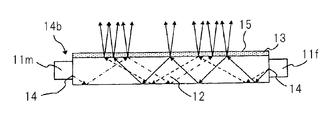
- light output from, for example, light-emitting element 11 f among the plurality of light-emitting elements 11 is transmitted through light incident surface 14 of light guide body 12 , and propagated in light guide body 12 in a condition of total reflection.
- a part of the light incident on the interface between light guide body 12 and directional control layer 13 is output from light exit part 15 with a wavelength in a direction corresponding to characteristics, described below, of plasmon excitation layer 17 of directional control layer 13 .
- Light not output from light exit part 15 is returned to light guide body 12 , and a part of the light incident on the interface between light guide body 12 and directional control layer 13 is transmitted again through directional control layer 13 and output from light exit part 15 .
- light exit part 15 Light output from, among the plurality of light-emitting elements 11 , light-emitting element 11 m located opposite light-emitting element 11 f that sandwiches light guide body 12 and that is transmitted through light incident surface 14 is similarly output from light exit part 15 .
- the direction and wavelength of the light output from light exit part 15 depend only on the characteristics of directional control layer 13 . The direction and the wavelength of this light are not dependent on the location of light-emitting element 11 and an incident angle on the interface between light guide body 12 and directional control layer 13 .
- wave vector conversion layer 18 has a photonic crystal structure
- the condition of total reflection is broken on the interface between light guide body 12 and carrier generation layer 16 , and the light from light-emitting element 11 enters into carrier generation layer 16 .
- the light incident on carrier generation layer 16 generates carriers in carrier generation layer 16 .
- the generated carrier causes plasmon coupling with free electrons in plasmon excitation layer 17 .
- surface plasmon is excited on the interface between plasmon excitation layer 17 and wave vector conversion layer 18 .
- the excited surface plasmon is diffracted by wave vector conversion layer 18 to exit from light source device 2 .
- the surface plasmon generated on the interface cannot be removed.
- the surface plasmon can be diffracted to be removed as light.
- the light output from one point of wave vector conversion layer 18 has an annular intensity distribution where the light concentrically spreads while being propagated.
- a center exit angle ⁇ rad of the light output from wave vector conversion layer 18 is represented by the following formula (5), in which ⁇ is a pitch of the periodic structure of wave vector conversion layer 18 , and i is a positive or negative integer:
- FIGS. 6A to 6G show a manufacturing process of optical element 1 included in light source device 2 .
- This process is only an example, and thus the present invention is not limited to this manufacturing method.
- carrier generation layer 16 is deposited on light guide body 12 by spin-coating.
- plasmon excitation layer 17 is formed on carrier generation layer 16 by, for example, physical vapor deposition, electron beam deposition, or sputtering.
- wave vector conversion layer 1 is formed on carrier generation layer 16 by a photonic crystal.
- resist film 21 is deposited on wave vector conversion layer 18 by spin coating.
- the negative pattern of the photonic crystal is transferred to resist film 21 by nano-imprinting.
- wave vector conversion layer 18 is etched to a desired depth by dry etching.
- resist film 12 is peeled off from wave vector conversion layer 18 .
- a plurality of light-emitting elements 11 is arranged on the outer circumferential surface of light guide body 12 to complete light source device 2 .
- light source device 2 has a relatively simple configuration that includes directional control layer 13 formed in light guide body 12 , and hence entire light source device 2 can be miniaturized.
- the exit angle of the light output from wave vector conversion layer 18 is determined by the complex dielectric constant of plasmon excitation layer 17 , the effective dielectric constant of the incident side portion and the effective dielectric constant of the exit side portion sandwiching plasmon excitation layer 17 , and a light emission spectrum of light generated in light source device 2 .
- directionality of the light output from optical element 1 is not limited by that of light-emitting element 11 .
- the etendue of the light output from light source device 2 can be reduced without any dependence on the etendue of light-emitting element 11 .
- the etendue of the light output from light source device 2 is not limited by the etendue of light-emitting element 11 .
- lights incident from the plurality of light-emitting elements 11 can be synthesized while maintaining a small etendue of the light output from light source device 2 .
- the configuration disclosed in Japanese Patent Application Laid-Open No. 2009-87695 has a problem, namely, the bending of the lights from the plurality of LEDs 300 in various directions at cross prism sheets 304 and 305 causes light loss.
- optical element 1 of the present embodiment use efficiency of the lights from the plurality of light-emitting elements 11 can be improved.
- light source devices of other embodiments will be described.
- the light source devices of the other embodiments are different only as regards the configuration of directional control layer 13 from light source device 2 of the first embodiment, and thus only the directional control layer will be described.
- layers similar to those of directional control layer 13 of the first embodiment are denoted by reference numerals similar to those of the first embodiment, and will not be described.
- FIG. 7 is a perspective view schematically showing a directional control layer included in a light source device according to a second embodiment.
- wave vector conversion layer 28 including a microlens array is disposed on the surface of plasmon excitation layer 17 .
- directional control layer 23 can provide the same effects as those in the configuration that includes wave vector conversion layer 18 made of the photonic crystal.
- FIGS. 8A and 8B are explanatory sectional views showing the manufacturing process of a configuration where the microlens array is stacked on plasmon excitation layer 17 .
- carrier generation layer 16 and plasmon excitation layer 17 are stacked on light guide body 12 , and thus description of the manufacturing process thereof will be omitted.
- wave vector conversion layer 28 is formed on the surface of plasmon excitation layer 17 by the microlens array.
- This forming method is only an example, and thus the present invention is not limited to this method.
- UV (ultraviolet) cured resin 31 is deposited on the surface of the plasmon excitation layer 17 by spin-coating. Then, by using nano-printing, the desired lens array pattern is formed in UV cured resin 31 . UV cured resin 31 is then irradiated with light to form a microlens array.
- directional control layer 23 of the second embodiment thus configured, by including wave vector conversion layer 28 that includes the microlens array, the same effects as those of the first embodiment can be provided.
- wave vector conversion layer 18 is made of a photonic crystal.
- wave vector conversion layer 18 can be substituted with wave vector conversion layer 28 including a microlens array, and effects similar to those of each embodiment can be provided.
- FIG. 9 is a perspective view showing a directional control layer included in a light source device according to a third embodiment.
- carrier generation layer 16 plasmon excitation layer 17 , dielectric constant layer 19 , and wave vector conversion layer 18 are stacked in order on light guide body 12 .
- the third embodiment is different from the first embodiment in that dielectric constant layer 19 is independently disposed between plasmon excitation layer 17 and wave vector conversion layer 18 .
- Dielectric constant layer 19 has a dielectric constant set lower than that of dielectric constant layer 20 (high dielectric constant layer 20 ) in a fourth embodiment described below, and thus will be referred to as low dielectric constant layer 19 .
- the dielectric constant of low dielectric constant layer 19 a range where the effective dielectric constant of the exit side portion is maintained lower than that of the effective dielectric constant of the incident side portion with respect to plasmon excitation layer 17 is permitted. In other words, the dielectric constant of low dielectric constant layer 19 does not need to be smaller than the effective dielectric constant of the incident side portion with respect to plasmon excitation layer 17 .
- Low dielectric constant layer 19 can be made of a material different from that of wave vector conversion layer 18 .
- the freedom of material selection can be increased for wave vector conversion layer 18 .
- low dielectric constant layer 19 preferably, a thin film or a porous film made of, for example, SiO 2 , AlF 3 , MgF 2 , Na 3 AlF 6 , NaF, LiF, CaF 2 , BaF 2 , and low dielectric constant plastic, is used.
- Low dielectric constant layer 19 is desirably thin as much as possible.
- the permitted maximum value of the thickness corresponds to the steeping length of the surface plasmon in the thickness direction of low dielectric constant layer 19 , and is calculated by using formula (4). When the thickness of low dielectric constant layer 19 exceeds the value calculated by formula (4), it is difficult to remove the surface plasmon as light.
- the effective dielectric constant of the incident side portion including light guide body 12 and carrier excitation layer 16 is set higher than that of the exit side portion including wave vector conversion layer 18 and low dielectric constant layer 19 and the medium in contact with t wave vector conversion layer 18 .
- FIG. 10 is a perspective view showing a directional control layer included in a light source device according to the fourth embodiment.
- carrier generation layer 16 dielectric constant layer 20 , plasmon excitation layer 17 , and wave vector conversion layer 18 made of photonic crystal are stacked in order on light guide body 12 .
- the fourth embodiment is different from the first embodiment in that dielectric constant layer 20 is independently disposed between plasmon excitation layer 17 and wave vector conversion layer 18 .
- Dielectric constant layer 20 has a dielectric constant set higher than that of low dielectric constant layer 19 in the third embodiment, and thus will be referred to as high dielectric constant layer 20 .
- high dielectric constant layer 20 For the dielectric constant of high dielectric constant layer 20 , a range where the effective dielectric constant of the exit side portion is maintained lower than that of the effective dielectric constant of the incident side portion with respect to plasmon excitation layer 17 is permitted. In other words, the dielectric constant of high dielectric constant layer 20 does not need to be larger than the effective dielectric constant of the exit side portion with respect to plasmon excitation layer 17 .
- High dielectric constant layer 20 can be made of a material different from that of carrier generation layer 16 .
- the freedom of material selection can be increased for carrier generation layer 16 .
- high dielectric constant layer 20 preferably, a thin film or a porous film made of a high dielectric constant material such as TiO 2 , CeO 2 , Ta 2 O 5 , ZrO 2 , Sb 2 O 3 , HfO 2 , La2O 3 , NdO 3 , Y 2 O 3 , ZnO, Nb 2 O 5 is used.
- High dielectric constant layer 20 is preferably made of a conductive material. High dielectric constant layer 20 is desirably as thin as possible. The permitted maximum value of the thickness corresponds to distance causing plasmon coupling between carrier generation layer 16 and plasmon excitation layer 17 , and is calculated by formula (4).
- the effective dielectric constant of the incident side portion including light guide body 12 , carrier excitation layer 16 , and high dielectric constant layer 20 is set higher than that of the exit side portion including wave vector conversion layer 18 and the medium in contact with t wave vector conversion layer 18 .
- FIG. 11 is a perspective view showing a directional control layer included in a light source device according to the fifth embodiment.
- directional control layer 53 includes low dielectric constant layer 19 sandwiched between plasmon excitation layer 17 and wave vector conversion layer 18 , and high dielectric constant layer 20 sandwiched between carrier generation layer 16 and plasmon excitation layer 17 and having a dielectric constant higher than that of low dielectric constant layer 19 .
- the effective dielectric constant of the incident side portion including light guide body 12 , carrier excitation layer 16 , and high dielectric constant layer 20 is set higher than that of the exit side portion including wave vector conversion layer 18 , low dielectric constant layer 19 , and the medium contacted with wave vector conversion layer 18 .
- directional control layer 53 of the fifth embodiment effects similar to those of the first embodiment can be provided, and the inclusion of independent low dielectric constant layer 19 and high dielectric constant layer 20 facilitates adjustment of the effective dielectric constant of the exit side portion of plasmon excitation layer 17 and the effective dielectric constant of the incident side portion of plasmon excitation layer 17 .
- Directional control layer 53 of the fifth embodiment can provide the same effects as those of the first embodiment.
- low dielectric constant layer 19 is located on wave vector conversion layer 18 side of plasmon excitation layer 17
- high dielectric layer 20 is located on carrier generation layer 16 side of plasmon excitation layer 17 .
- the present invention is not limited to this configuration. To set the effective dielectric constant of the incident side portion of plasmon excitation layer 17 higher than that of the effective dielectric constant of the exit side portion of plasmon excitation layer 17 , when necessary, the arrangement of low dielectric constant layer 19 and high dielectric constant layer 20 with respect to plasmon excitation layer 17 can be reversed from that of the fifth embodiment.
- FIG. 11 is a perspective view showing the directional control layer included in a light source device according to the sixth embodiment.
- directional control layer 63 according to the sixth embodiment is similar in configuration to directional control layer 53 of the fifth embodiment, but is different in that each of low dielectric constant layer 19 and high dielectric constant layer 20 is configured by stacking a plurality of dielectric layers.
- directional control layer 63 includes low dielectric constant layer group 29 formed by stacking a plurality of dielectric layers 29 a to 29 c and high dielectric constant layer group 30 formed by stacking a plurality of dielectric layers 30 a to 30 c.
- the plurality of dielectric layers 29 a to 29 c are arranged so that dielectric constants can be monotonously decreased from near plasmon excitation layer 17 to wave vector conversion layer 18 side.
- the plurality of dielectric layers 30 a to 30 c are arranged so that dielectric constants can be monotonously increased from near carrier generation layer 16 to plasmon excitation layer 17 .
- the overall thickness of low dielectric constant layer group 29 is equal to the thickness of the low dielectric constant layer in an embodiment where the directional control layer independently includes the low dielectric constant layer.
- the overall thickness of high dielectric constant layer group 30 is equal to the thickness of the high dielectric constant layer in an embodiment where the directional control layer independently includes the high dielectric constant layer.
- Each of low dielectric constant layer group 29 and high dielectric constant layer group 30 is shown to have a three-layer structure. However, for example, a layer structure having two to five layers can be employed.
- a configuration where the numbers of dielectric layers included in the low dielectric constant layer group and the high dielectric constant layer group are different or a configuration where only the low dielectric constant layer or the high dielectric constant layer includes a plurality of dielectric constant layers can be employed.
- high dielectric layer constant group 30 can reduce the refractive index difference from wave vector conversion layer 18 or a medium such as air on the interface, while low dielectric layer constant group 29 can reduce the refractive index difference from carrier generation layer 16 on the interface.
- the appropriate dielectric constant of each dielectric layer adjacent to plasmon excitation layer 17 can be set, and refractive index differences from carrier generation layer 16 and wave vector conversion layer 18 on the interface can be set small. As a result, light losses can be further reduced, and use efficiency of the light from light-emitting element 11 can be improved.
- a single-layer film having a dielectric constant monotonously changed therein can be used.
- a high dielectric constant layer has a dielectric constant distribution gradually increased from carrier generation layer 16 side to plasmon excitation layer 17 side.
- a low dielectric constant layer has a dielectric constant distribution gradually reduced from plasmon excitation layer 17 side to wave vector conversion layer 18 side.
- FIG. 13 is a perspective view showing a directional control layer included in a light source device according to the seventh embodiment.
- directional control layer 73 according to the seventh embodiment is similar in configuration to directional control layer 13 of the first embodiment, but different in that plasmon excitation layer group 37 includes a plurality of stacked metal layers 37 a and 37 b.
- metal layers 37 a and 37 b are made of different metallic materials to be stacked. This enables plasmon excitation layer group 37 to adjust the plasma frequency.
- metal layers 37 a and 37 b are respectively made of Ag and Al.
- metal layers 37 a and 37 b are respectively made of Ag and Au.
- Plasmon excitation layer group 37 is shown to have a two-layered structure as an example.
- Plasmon excitation layer group 37 can include three or more metal layers when necessary. Plasmon excitation layer group 37 is preferably formed with a thickness equal to or less than 200 nanometers, more preferably about 10 nanometers to 100 nanometers.
- plasmon excitation layer group 37 includes the plurality of metal layers 37 a and 37 b . This enables adjustment of an effective plasma frequency on plasmon excitation layer 37 close to the frequency of light incident on plasmon excitation layer group 37 from carrier generation layer 16 . As a result, use efficiency of the light incident on optical element 1 from light-emitting element 11 can be further improved.
- FIG. 14 is a perspective view showing the directional control layer included in the light source device according to the eighth embodiment.
- directional control layer 83 according to the eighth embodiment includes plasmon excitation layer 27 as another plasmon excitation layer in addition to plasmon excitation layer 17 of the first embodiment.
- plasmon excitation layer 27 is disposed between carrier generation layer 16 and light guide body 12 .
- a plasmon is excited on plasmon excitation layer 27 by light that enters from light guide body 12 , and carriers are generated on carrier generation layer 16 by the excited plasmon.
- a dielectric constant of carrier generation layer 16 is set lower than that of light guide body 12 .
- a low dielectric constant layer where the real part of a complex dielectric constant is lower than light guide body 12 can be disposed between plasmon excitation layer 27 and carrier generation layer 16 .
- Plasmon excitation layer 27 has a plasma frequency higher than the light emission frequency generated when excitation occurs on single carrier generation layer 16 by light from light-emitting element 11 . Plasmon excitation layer 27 has a plasma frequency higher than the light emission frequency of light-emitting element 11 .
- carrier generation layer 16 having a plurality of different light emission frequencies is used, plasmon excitation layer 27 has a plasma frequency higher than any one of light emission frequencies of light generated when excitation occurs on single carrier generation layer 16 by light from light-emitting element 11 .
- plasmon excitation layer 27 has a plasma frequency higher than any one of the different light emission frequencies of the light-emitting elements.
- carriers can be efficiently generated on carrier generation layer 16 by the fluorescence enhancement effect of the plasmon, increasing the number of carriers, use efficiency of the light from light-emitting element 11 can be increased more.
- plasmon excitation layer 27 can be configured by stacking a plurality of metal layers.
- FIG. 15 is a perspective view showing a directional control layer included in a light source device according to the ninth embodiment.
- directional control layer 93 according to the ninth embodiment is similar in configuration to directional control layer 13 of the first embodiment, but different in that low dielectric constant layer 39 is disposed between carrier generation layer 16 and light guide body 12 to operate differently from low dielectric constant layer 19 of the aforementioned embodiment.
- low dielectric constant layer 39 is located directly below carrier generation layer 16 .
- a dielectric constant of low dielectric constant layer 93 is set lower than that of light guide body 12 .
- the incident angle with respect to light incident surface 14 of light guide body 12 is set to a predetermined angle so that light incident from light-emitting element 11 can be in a condition of total reflection on the interface between light guide body 12 and low dielectric constant layer 39 .
- the light incident on light guide body 12 from light-emitting element 11 is in a condition of total reflection on the interface between light guide body 12 and low dielectric constant layer 39 . This total-reflection is accompanied by the generation of an evanescent wave.
- the evanescent wave acts on carrier generation layer 16 to generate carriers in carrier generation layer 16 .
- a part of the light output from light-emitting element 11 is transmitted through each layer and exits from each layer.
- two types of lights that are different by 30 nanometers to 300 nanometers in wavelength are caused to exit from the light source device.
- the light corresponding to the emission wavelength of carrier generation layer 16 can be increased while the light corresponding to the emission wavelength of light-emitting element 11 is reduced.
- use efficiency of the light from light-emitting element 11 can be improved.
- FIG. 16 is a perspective view showing a light source unit according to the tenth embodiment.
- the light source unit according to the tenth embodiment includes, as a polarizing conversion element for arranging axially symmetric polarized light incident from optical element 1 in a predetermined polarized state, axially symmetric polarization 1 ⁇ 2 wavelength plate 100 for linearly polarizing the light incident from optical element 1 .
- Linearly polarizing light output from light source device 2 by axially symmetric polarization 1 ⁇ 2 wavelength plate 100 can realize a light source unit, where a polarized state of the output light is uniform.
- Arranging the axially symmetric polarized light in the predetermined state by the polarizing conversion element is not limited to linear polarizing. Circular polarizing is also included.
- a directional control layer included in the light guide device of the present embodiment needless to say, any of the directional control layers according to the first to ninth embodiments can be applied.
- FIG. 17 is a vertical sectional view showing the structure of 1 ⁇ 2 wavelength plate 100 for axially symmetric polarization.
- the configuration of axially symmetric polarization 1 ⁇ 2 wavelength plate 100 is only an example, and thus is in no way limitative.
- axially symmetric polarization 1 ⁇ 2 wavelength plate 100 includes a pair of glass substrates 101 and 106 in which oriented films 102 and 105 are respectively formed, liquid crystal layer 104 located by sandwiching oriented films 102 and 105 of glass substrates 101 and 106 opposite each other between glass substrates 101 and 106 , and spacer 103 located between glass substrates 101 and 106 .
- a refractive index ne is larger than a refractive index no, where no is the refractive index for ordinary light, and ne is the refractive index for extraordinary light.
- FIGS. 18A and 18B are explanatory schematic views showing axially symmetric polarization 1 ⁇ 2 wavelength plate 100 .
- FIG. 18A is a transverse sectional view showing a state where liquid crystal layer 104 of axially symmetric polarization 1 ⁇ 2 wavelength plate 100 is cut in parallel to the principal surface of glass substrate 101 .
- FIG. 18B is an explanatory schematic view showing the light direction of liquid crystal molecules 107 .
- liquid crystal molecules 107 are concentrically arranged around axially symmetric polarization 1 ⁇ 2 wavelength plate 100 .
- FIGS. 18A and 18B show the inside of the same plane.
- FIG. 19 shows far-field pattern 109 of output light when the light source device does not include axially symmetric polarization 1 ⁇ 2 wavelength plate 100 .
- far-field pattern 109 of the output light from the light source device becomes axially polarized light where polarizing direction 108 is radial around the optical axis of the light output from the light source device.
- FIG. 20 shows far-field pattern 109 of output light that passes through axially symmetric polarization 1 ⁇ 2 wavelength plate 100 .
- the use of axially symmetric polarization 1 ⁇ 2 wavelength plate 100 enables acquisition of output light where polarizing direction 110 is uniform.
- FIG. 21 shows the angle distribution in the output light of the light source device according to the first embodiment.
- a horizontal axis indicates the exit angle of output light
- the vertical axis indicates the intensity of the output light.
- SiO 2 a phosphor of base material PVA (polyvinyl alcohol), Ag, and PMMA (polymethylmethacrylate) were respectively used for light guide body 12 , carrier generation layer 16 , plasmon excitation layer 17 , and wave vector conversion layer 18 , and thicknesses thereof were respectively set to 0.5 millimeters, 100 nanometers, 50 nanometers, and 100 nanometers. Calculation was carried out with the emission wavelength of carrier generation layer 16 set to 460 nanometers. In this case, the depth, the pitch, and the duty ratio of the periodic structure of wave vector conversion layer 18 were respectively set to 100 nanometers, 325 nanometers, and 0.5. The output light under these conditions has an light distribution not annular but near a gauss function. However, by shifting the pitch by 325 nanometers, the peak is broken, and annular light distribution can be acquired.
- PVA polyvinyl alcohol
- Ag silver
- PMMA polymethylmethacrylate
- directionality by enhancing directionality of the emission angle of the output light from light source device 2 and by appropriately adjusting the grating structure of wave vector conversion layer 18 to narrow the emission angle by ⁇ 5 degrees, directionality can be further improved.
- FIG. 22 shows the angle distribution in the output light of the light source device according to the fifth embodiment.
- a horizontal axis indicates the exit angle of output light
- a vertical axis indicates the intensity of the output light.
- SiO 2 a phosphor of a base material PVA (polyvinyl alcohol), Al 2 O 3 , Ag, and porous SiO 2 were respectively used for light guide body 12 , carrier generation layer 16 , high dielectric constant layer 20 , plasmon excitation layer 17 , and low dielectric constant layer 19 , and thicknesses thereof were respectively set to 0.5 millimeters, 100 nanometers, 10 nanometers, 50 nanometers, and 10 nanometers.
- the dielectric constant of porous SiO 2 was set to 1.12.
- Example 2 As a material of wave vector conversion layer 18 , PMMA (polymethylmethacrylate) was used, and the depth, the pitch, and the duty ratio of the periodic structure were respectively set to 100 nanometers, 421 nanometers, and 0.5.
- the output light under these conditions does not have a annular light distribution but has a light distribution which is near a gauss function. However, by shifting the pitch by 421 nanometers, a peak is broken, and an annular light distribution can be acquired.
- Example 2 by arranging high dielectric constant layer 20 and low dielectric constant layer 19 to sandwich plasmon excitation layer 17 , light distribution having directionality higher than that of Example 1 was acquired.
- the effective dielectric constants of the exit side portion and the incident side portion of plasmon excitation layer 17 are respectively set to 1.48 and 2.52 by formula (1).
- the imaginary parts of z-direction wave numbers on the exit side and the incident side of the surface plasmon are respectively set to 8.96 ⁇ 10 6 and 1.71 ⁇ 10 7 by formula (2).
- the effective interactive distance of the surface plasmon is a distance where the intensity of the surface plasmon is e ⁇ 2 , by 1/1 meters (k spp,z )
- the effective interactive distances of the surface plasmon are respectively 112 nanometers and 58 nanometers on the exit side and the incident side.
- FIG. 23 shows comparison of a plasmon resonance angle ( ⁇ in the drawing) obtained from an effective dielectric constant calculated by using formula (1) with a plasmon resonance angle ( ⁇ in the drawing) obtained from multilayer film reflection calculation in light source device 2 according to the fifth embodiment.
- Calculation conditions are similar to those except for the thickness of low dielectric constant layer 19 when the angle distribution was calculated.
- a horizontal axis indicates the thickness of low dielectric constant layer 19
- a vertical axis indicates the plasmon resonance angle.
- the value calculated by an effective dielectric constant and the value calculated by multilayer film reflection match each other, and the condition of plasmon resonance can apparently be defined by the effective dielectric constant defined by formula (1).
- the light source device which is suitably used as a light source device of an image display device, can be used for a light source device included in a projection display device, a near-field light source device of a liquid crystal panel (LCD), a mobile phone as a backlight, and an electronic device such as a PDA (Personal Data Assistant).
- a light source device included in a projection display device a near-field light source device of a liquid crystal panel (LCD), a mobile phone as a backlight, and an electronic device such as a PDA (Personal Data Assistant).
- LCD liquid crystal panel
- PDA Personal Data Assistant
- FIG. 24 is a perspective view schematically showing the LED projector of the embodiment.
- the LED projector includes red (R) light source device 2 r , green (G) light source device 2 g , and blue (B) light source device 2 b , illumination optical systems 120 r , 120 g , and 120 b into which lights output from light source devices 2 r , 2 g , and 2 b enter, and light valves 121 r , 121 g , and 121 B as display elements into which the lights that passes through illumination optical systems 120 r , 120 g , and 120 b enter.
- R red
- G green
- B blue
- the LED projector further includes cross dichroic prism 122 that synthesizes R, G, and B lights entered after modulation by light valves 121 r , 121 g , and 121 b , and projection optical system 123 that includes a projection lens (not shown) for projecting the light output from cross dichroic prism 122 to a projection surface such as a screen.
- cross dichroic prism 122 that synthesizes R, G, and B lights entered after modulation by light valves 121 r , 121 g , and 121 b
- projection optical system 123 that includes a projection lens (not shown) for projecting the light output from cross dichroic prism 122 to a projection surface such as a screen.
- Illumination optical systems 120 r , 120 g , and 120 b include, for example, rod lenses (not shown) for making luminance uniform.
- Light valves 121 r , 121 g , and 121 b include, for example, liquid crystal display plates or DMDs. Needless to say, the light source device of the abovementioned embodiment can be applied to a single-plate projector.
- the luminance of a projected image can be improved.
- axially symmetric polarization 1 ⁇ 2 wavelength plate 100 shown in FIG. 17 and FIGS. 18A and 18B is preferably located on the optical path of the light output from each of light source devices 2 r , 2 g , and 2 b . This can suppress polarized light loss at light valves 121 r , 121 g , and 121 b .
- the illumination optical system includes a polarizer
- axially symmetric polarization 1 ⁇ 2 wavelength plate 100 is preferably located between the polarizer and light source device 2 .
Landscapes
- Physics & Mathematics (AREA)
- Engineering & Computer Science (AREA)
- Nanotechnology (AREA)
- Optics & Photonics (AREA)
- Chemical & Material Sciences (AREA)
- Crystallography & Structural Chemistry (AREA)
- Biophysics (AREA)
- Life Sciences & Earth Sciences (AREA)
- General Physics & Mathematics (AREA)
- Planar Illumination Modules (AREA)
- Optical Modulation, Optical Deflection, Nonlinear Optics, Optical Demodulation, Optical Logic Elements (AREA)
- Non-Portable Lighting Devices Or Systems Thereof (AREA)
- Projection Apparatus (AREA)
Applications Claiming Priority (3)
| Application Number | Priority Date | Filing Date | Title |
|---|---|---|---|
| JP2010-047944 | 2010-03-04 | ||
| JP2010047944 | 2010-03-04 | ||
| PCT/JP2010/068012 WO2011108138A1 (ja) | 2010-03-04 | 2010-10-14 | 光学素子、光源装置及び投射型表示装置 |
Publications (2)
| Publication Number | Publication Date |
|---|---|
| US20130033678A1 US20130033678A1 (en) | 2013-02-07 |
| US9116270B2 true US9116270B2 (en) | 2015-08-25 |
Family
ID=44541813
Family Applications (1)
| Application Number | Title | Priority Date | Filing Date |
|---|---|---|---|
| US13/580,697 Active 2031-10-30 US9116270B2 (en) | 2010-03-04 | 2010-10-14 | Optical element, light source device, and projection display device |
Country Status (4)
| Country | Link |
|---|---|
| US (1) | US9116270B2 (zh) |
| JP (1) | JP5605426B2 (zh) |
| CN (1) | CN102782394B (zh) |
| WO (1) | WO2011108138A1 (zh) |
Cited By (1)
| Publication number | Priority date | Publication date | Assignee | Title |
|---|---|---|---|---|
| US20150301282A1 (en) * | 2012-07-31 | 2015-10-22 | Nec Corporation | Optical element, illumination device, image display device, method of operating optical element |
Families Citing this family (11)
| Publication number | Priority date | Publication date | Assignee | Title |
|---|---|---|---|---|
| US9039201B2 (en) * | 2010-05-14 | 2015-05-26 | Nec Corporation | Display element, display device, and projection display device |
| CN103154804B (zh) * | 2010-10-15 | 2015-12-02 | 日本电气株式会社 | 光学装置、光源以及投影型显示装置 |
| JPWO2012137583A1 (ja) * | 2011-04-07 | 2014-07-28 | 日本電気株式会社 | 光学素子、カラーホイール、照明装置および投射型表示装置 |
| WO2012172858A1 (ja) * | 2011-06-17 | 2012-12-20 | 日本電気株式会社 | 光学素子、光源装置及び投射型表示装置 |
| US20140226197A1 (en) * | 2011-09-27 | 2014-08-14 | Nec Corporation | Optical element and projection-type display device using same |
| WO2014013712A1 (ja) * | 2012-07-19 | 2014-01-23 | 日本電気株式会社 | 光学装置およびそれを用いた表示装置 |
| FR3000811B1 (fr) * | 2013-01-07 | 2015-01-30 | Peugeot Citroen Automobiles Sa | Systeme de signalisation holographique comprenant une unite de generation d'au moins une image holographique |
| US9851497B2 (en) * | 2014-06-11 | 2017-12-26 | Samsung Electronics Co., Ltd. | Light mixing chamber for use with color converting material and light guide plate and assembly |
| US10739110B2 (en) * | 2016-11-10 | 2020-08-11 | Kiho Military Acquisition Consulting, Inc. | Composite telescopic sight, sight mount, and electroluminescent digitally adjustable reticle |
| US10641115B2 (en) * | 2017-08-29 | 2020-05-05 | United Technologies Corporation | Segmented conduit with airfoil geometry |
| JP7007923B2 (ja) * | 2018-01-16 | 2022-01-25 | 日機装株式会社 | 半導体発光素子および半導体発光素子の製造方法 |
Citations (9)
| Publication number | Priority date | Publication date | Assignee | Title |
|---|---|---|---|---|
| CN1216114A (zh) | 1996-02-29 | 1999-05-05 | 美国3M公司 | 增亮膜 |
| JP2001067685A (ja) | 1999-09-01 | 2001-03-16 | Sharp Corp | 光学装置 |
| JP2002063722A (ja) | 2000-08-21 | 2002-02-28 | Taiyo Yuden Co Ltd | 光情報記録方法および光情報記録媒体 |
| US20030184989A1 (en) | 2002-03-29 | 2003-10-02 | Citizen Watch Co., Ltd. & Citizen Electronics Co., Ltd. | Lighting device for lighting a liquid crystal display |
| US20060278888A1 (en) * | 2005-05-31 | 2006-12-14 | Samsung Electro-Mechanics Co., Ltd. | Vertically-structured nitride semiconductor light emitting diode |
| US20070181889A1 (en) * | 2006-02-08 | 2007-08-09 | Kenji Orita | Semiconductor light emitting device and method for manufacturing the same |
| JP2008145510A (ja) | 2006-12-06 | 2008-06-26 | Casio Comput Co Ltd | 光源ユニット及びプロジェクタ |
| US20090086477A1 (en) * | 2007-09-28 | 2009-04-02 | Citizen Electronics Co., Ltd. | Planar light source and method of manufacturing planar light source |
| CN102549328A (zh) | 2009-09-30 | 2012-07-04 | 日本电气株式会社 | 光学元件、光源装置以及投射显示装置 |
-
2010
- 2010-10-14 JP JP2012502958A patent/JP5605426B2/ja not_active Expired - Fee Related
- 2010-10-14 WO PCT/JP2010/068012 patent/WO2011108138A1/ja active Application Filing
- 2010-10-14 CN CN201080065176.5A patent/CN102782394B/zh not_active Expired - Fee Related
- 2010-10-14 US US13/580,697 patent/US9116270B2/en active Active
Patent Citations (12)
| Publication number | Priority date | Publication date | Assignee | Title |
|---|---|---|---|---|
| CN1216114A (zh) | 1996-02-29 | 1999-05-05 | 美国3M公司 | 增亮膜 |
| JP2001067685A (ja) | 1999-09-01 | 2001-03-16 | Sharp Corp | 光学装置 |
| JP2002063722A (ja) | 2000-08-21 | 2002-02-28 | Taiyo Yuden Co Ltd | 光情報記録方法および光情報記録媒体 |
| US20030184989A1 (en) | 2002-03-29 | 2003-10-02 | Citizen Watch Co., Ltd. & Citizen Electronics Co., Ltd. | Lighting device for lighting a liquid crystal display |
| JP2003295183A (ja) | 2002-03-29 | 2003-10-15 | Citizen Watch Co Ltd | 液晶表示装置の平面照明装置 |
| US20060278888A1 (en) * | 2005-05-31 | 2006-12-14 | Samsung Electro-Mechanics Co., Ltd. | Vertically-structured nitride semiconductor light emitting diode |
| US20070181889A1 (en) * | 2006-02-08 | 2007-08-09 | Kenji Orita | Semiconductor light emitting device and method for manufacturing the same |
| JP2008145510A (ja) | 2006-12-06 | 2008-06-26 | Casio Comput Co Ltd | 光源ユニット及びプロジェクタ |
| US20090086477A1 (en) * | 2007-09-28 | 2009-04-02 | Citizen Electronics Co., Ltd. | Planar light source and method of manufacturing planar light source |
| JP2009087695A (ja) | 2007-09-28 | 2009-04-23 | Citizen Electronics Co Ltd | 面光源装置及び面光源装置の製造方法 |
| CN102549328A (zh) | 2009-09-30 | 2012-07-04 | 日本电气株式会社 | 光学元件、光源装置以及投射显示装置 |
| US20120176766A1 (en) * | 2009-09-30 | 2012-07-12 | Nec Corporation | Optical element, light source device, and projection display device |
Non-Patent Citations (4)
| Title |
|---|
| Chinese Office Action for CN Application No. 201080065176.5 issued on Mar. 21, 2014 with English Translation. |
| PhlatLight TM Photonic Grating LEDs for RPTV Light Engines Christian Hoepfner, SID Symposium Digest 37, 1808 (2006). |
| The international search report for PCT/JP2010/068012 dated Nov. 16, 2010. |
| Wang, Guo-Xung et al. "The Research of MEMS Infrared Radiation Source Characteristics Based on Surface Plasmon Resonance Effect" Chinese Journal of Sensors and Actuators, Aug. 2008, vol. 21, No. 8, pp. 1353-1356, with English Abstract. |
Cited By (1)
| Publication number | Priority date | Publication date | Assignee | Title |
|---|---|---|---|---|
| US20150301282A1 (en) * | 2012-07-31 | 2015-10-22 | Nec Corporation | Optical element, illumination device, image display device, method of operating optical element |
Also Published As
| Publication number | Publication date |
|---|---|
| US20130033678A1 (en) | 2013-02-07 |
| JP5605426B2 (ja) | 2014-10-15 |
| CN102782394B (zh) | 2015-05-20 |
| CN102782394A (zh) | 2012-11-14 |
| WO2011108138A1 (ja) | 2011-09-09 |
| JPWO2011108138A1 (ja) | 2013-06-20 |
Similar Documents
| Publication | Publication Date | Title |
|---|---|---|
| US9146350B2 (en) | Optical element, light source device, and projection display device | |
| US9116270B2 (en) | Optical element, light source device, and projection display device | |
| US9028071B2 (en) | Light emitting element, light source device, and projection display device | |
| US9170351B2 (en) | Optical element, light source apparatus, and projection-type display apparatus | |
| US11442222B2 (en) | Evacuated gratings and methods of manufacturing | |
| US7573546B2 (en) | Wire grid polarizer having dual layer structure and method of fabricating the same | |
| JP5664657B2 (ja) | 光学素子、光源および投射型表示装置 | |
| JP5605427B2 (ja) | 発光素子、光源装置及び投射型表示装置 | |
| JP5776689B2 (ja) | 表示素子、表示器及び投射型表示装置 | |
| US9041041B2 (en) | Optical device, optical element, and image display device | |
| WO2013046872A1 (ja) | 光学素子、光源装置及び投射型表示装置 | |
| WO2013046865A1 (ja) | 光学素子、光源装置及び投射型表示装置 | |
| WO2013103038A1 (ja) | 光学装置および画像表示装置 |
Legal Events
| Date | Code | Title | Description |
|---|---|---|---|
| AS | Assignment |
Owner name: NEC CORPORATION, JAPAN Free format text: ASSIGNMENT OF ASSIGNORS INTEREST;ASSIGNORS:NATSUMEDA, MASANAO;IMAI, MASAO;SAITOH, GOROH;AND OTHERS;REEL/FRAME:029110/0904 Effective date: 20121001 |
|
| STCF | Information on status: patent grant |
Free format text: PATENTED CASE |
|
| MAFP | Maintenance fee payment |
Free format text: PAYMENT OF MAINTENANCE FEE, 4TH YEAR, LARGE ENTITY (ORIGINAL EVENT CODE: M1551); ENTITY STATUS OF PATENT OWNER: LARGE ENTITY Year of fee payment: 4 |
|
| MAFP | Maintenance fee payment |
Free format text: PAYMENT OF MAINTENANCE FEE, 8TH YEAR, LARGE ENTITY (ORIGINAL EVENT CODE: M1552); ENTITY STATUS OF PATENT OWNER: LARGE ENTITY Year of fee payment: 8 |