US9111818B2 - Packaging substrate - Google Patents
Packaging substrate Download PDFInfo
- Publication number
- US9111818B2 US9111818B2 US14/018,757 US201314018757A US9111818B2 US 9111818 B2 US9111818 B2 US 9111818B2 US 201314018757 A US201314018757 A US 201314018757A US 9111818 B2 US9111818 B2 US 9111818B2
- Authority
- US
- United States
- Prior art keywords
- conductive
- packaging substrate
- substrate
- conductive pads
- pillars
- Prior art date
- Legal status (The legal status is an assumption and is not a legal conclusion. Google has not performed a legal analysis and makes no representation as to the accuracy of the status listed.)
- Expired - Fee Related
Links
Images


Classifications
-
- H—ELECTRICITY
- H01—ELECTRIC ELEMENTS
- H01L—SEMICONDUCTOR DEVICES NOT COVERED BY CLASS H10
- H01L24/00—Arrangements for connecting or disconnecting semiconductor or solid-state bodies; Methods or apparatus related thereto
- H01L24/01—Means for bonding being attached to, or being formed on, the surface to be connected, e.g. chip-to-package, die-attach, "first-level" interconnects; Manufacturing methods related thereto
- H01L24/10—Bump connectors ; Manufacturing methods related thereto
- H01L24/12—Structure, shape, material or disposition of the bump connectors prior to the connecting process
- H01L24/13—Structure, shape, material or disposition of the bump connectors prior to the connecting process of an individual bump connector
-
- H—ELECTRICITY
- H01—ELECTRIC ELEMENTS
- H01L—SEMICONDUCTOR DEVICES NOT COVERED BY CLASS H10
- H01L21/00—Processes or apparatus adapted for the manufacture or treatment of semiconductor or solid state devices or of parts thereof
- H01L21/02—Manufacture or treatment of semiconductor devices or of parts thereof
- H01L21/04—Manufacture or treatment of semiconductor devices or of parts thereof the devices having at least one potential-jump barrier or surface barrier, e.g. PN junction, depletion layer or carrier concentration layer
- H01L21/48—Manufacture or treatment of parts, e.g. containers, prior to assembly of the devices, using processes not provided for in a single one of the subgroups H01L21/06 - H01L21/326
- H01L21/4814—Conductive parts
- H01L21/4846—Leads on or in insulating or insulated substrates, e.g. metallisation
- H01L21/4853—Connection or disconnection of other leads to or from a metallisation, e.g. pins, wires, bumps
-
- H—ELECTRICITY
- H01—ELECTRIC ELEMENTS
- H01L—SEMICONDUCTOR DEVICES NOT COVERED BY CLASS H10
- H01L23/00—Details of semiconductor or other solid state devices
- H01L23/48—Arrangements for conducting electric current to or from the solid state body in operation, e.g. leads, terminal arrangements ; Selection of materials therefor
- H01L23/488—Arrangements for conducting electric current to or from the solid state body in operation, e.g. leads, terminal arrangements ; Selection of materials therefor consisting of soldered or bonded constructions
- H01L23/498—Leads, i.e. metallisations or lead-frames on insulating substrates, e.g. chip carriers
- H01L23/49811—Additional leads joined to the metallisation on the insulating substrate, e.g. pins, bumps, wires, flat leads
- H01L23/49816—Spherical bumps on the substrate for external connection, e.g. ball grid arrays [BGA]
-
- H—ELECTRICITY
- H01—ELECTRIC ELEMENTS
- H01L—SEMICONDUCTOR DEVICES NOT COVERED BY CLASS H10
- H01L23/00—Details of semiconductor or other solid state devices
- H01L23/48—Arrangements for conducting electric current to or from the solid state body in operation, e.g. leads, terminal arrangements ; Selection of materials therefor
- H01L23/488—Arrangements for conducting electric current to or from the solid state body in operation, e.g. leads, terminal arrangements ; Selection of materials therefor consisting of soldered or bonded constructions
- H01L23/498—Leads, i.e. metallisations or lead-frames on insulating substrates, e.g. chip carriers
- H01L23/49838—Geometry or layout
-
- H—ELECTRICITY
- H01—ELECTRIC ELEMENTS
- H01L—SEMICONDUCTOR DEVICES NOT COVERED BY CLASS H10
- H01L24/00—Arrangements for connecting or disconnecting semiconductor or solid-state bodies; Methods or apparatus related thereto
- H01L24/01—Means for bonding being attached to, or being formed on, the surface to be connected, e.g. chip-to-package, die-attach, "first-level" interconnects; Manufacturing methods related thereto
- H01L24/10—Bump connectors ; Manufacturing methods related thereto
- H01L24/11—Manufacturing methods
-
- H—ELECTRICITY
- H01—ELECTRIC ELEMENTS
- H01L—SEMICONDUCTOR DEVICES NOT COVERED BY CLASS H10
- H01L2224/00—Indexing scheme for arrangements for connecting or disconnecting semiconductor or solid-state bodies and methods related thereto as covered by H01L24/00
- H01L2224/01—Means for bonding being attached to, or being formed on, the surface to be connected, e.g. chip-to-package, die-attach, "first-level" interconnects; Manufacturing methods related thereto
- H01L2224/10—Bump connectors; Manufacturing methods related thereto
- H01L2224/11—Manufacturing methods
- H01L2224/113—Manufacturing methods by local deposition of the material of the bump connector
- H01L2224/1131—Manufacturing methods by local deposition of the material of the bump connector in liquid form
- H01L2224/1132—Screen printing, i.e. using a stencil
-
- H—ELECTRICITY
- H01—ELECTRIC ELEMENTS
- H01L—SEMICONDUCTOR DEVICES NOT COVERED BY CLASS H10
- H01L2224/00—Indexing scheme for arrangements for connecting or disconnecting semiconductor or solid-state bodies and methods related thereto as covered by H01L24/00
- H01L2224/01—Means for bonding being attached to, or being formed on, the surface to be connected, e.g. chip-to-package, die-attach, "first-level" interconnects; Manufacturing methods related thereto
- H01L2224/10—Bump connectors; Manufacturing methods related thereto
- H01L2224/11—Manufacturing methods
- H01L2224/114—Manufacturing methods by blanket deposition of the material of the bump connector
- H01L2224/1141—Manufacturing methods by blanket deposition of the material of the bump connector in liquid form
- H01L2224/11422—Manufacturing methods by blanket deposition of the material of the bump connector in liquid form by dipping, e.g. in a solder bath
-
- H—ELECTRICITY
- H01—ELECTRIC ELEMENTS
- H01L—SEMICONDUCTOR DEVICES NOT COVERED BY CLASS H10
- H01L2224/00—Indexing scheme for arrangements for connecting or disconnecting semiconductor or solid-state bodies and methods related thereto as covered by H01L24/00
- H01L2224/01—Means for bonding being attached to, or being formed on, the surface to be connected, e.g. chip-to-package, die-attach, "first-level" interconnects; Manufacturing methods related thereto
- H01L2224/10—Bump connectors; Manufacturing methods related thereto
- H01L2224/11—Manufacturing methods
- H01L2224/114—Manufacturing methods by blanket deposition of the material of the bump connector
- H01L2224/1146—Plating
- H01L2224/11462—Electroplating
-
- H—ELECTRICITY
- H01—ELECTRIC ELEMENTS
- H01L—SEMICONDUCTOR DEVICES NOT COVERED BY CLASS H10
- H01L2224/00—Indexing scheme for arrangements for connecting or disconnecting semiconductor or solid-state bodies and methods related thereto as covered by H01L24/00
- H01L2224/01—Means for bonding being attached to, or being formed on, the surface to be connected, e.g. chip-to-package, die-attach, "first-level" interconnects; Manufacturing methods related thereto
- H01L2224/10—Bump connectors; Manufacturing methods related thereto
- H01L2224/11—Manufacturing methods
- H01L2224/114—Manufacturing methods by blanket deposition of the material of the bump connector
- H01L2224/1146—Plating
- H01L2224/11464—Electroless plating
-
- H—ELECTRICITY
- H01—ELECTRIC ELEMENTS
- H01L—SEMICONDUCTOR DEVICES NOT COVERED BY CLASS H10
- H01L2224/00—Indexing scheme for arrangements for connecting or disconnecting semiconductor or solid-state bodies and methods related thereto as covered by H01L24/00
- H01L2224/01—Means for bonding being attached to, or being formed on, the surface to be connected, e.g. chip-to-package, die-attach, "first-level" interconnects; Manufacturing methods related thereto
- H01L2224/10—Bump connectors; Manufacturing methods related thereto
- H01L2224/11—Manufacturing methods
- H01L2224/116—Manufacturing methods by patterning a pre-deposited material
- H01L2224/1161—Physical or chemical etching
-
- H—ELECTRICITY
- H01—ELECTRIC ELEMENTS
- H01L—SEMICONDUCTOR DEVICES NOT COVERED BY CLASS H10
- H01L2224/00—Indexing scheme for arrangements for connecting or disconnecting semiconductor or solid-state bodies and methods related thereto as covered by H01L24/00
- H01L2224/01—Means for bonding being attached to, or being formed on, the surface to be connected, e.g. chip-to-package, die-attach, "first-level" interconnects; Manufacturing methods related thereto
- H01L2224/10—Bump connectors; Manufacturing methods related thereto
- H01L2224/11—Manufacturing methods
- H01L2224/116—Manufacturing methods by patterning a pre-deposited material
- H01L2224/1162—Manufacturing methods by patterning a pre-deposited material using masks
- H01L2224/11622—Photolithography
-
- H—ELECTRICITY
- H01—ELECTRIC ELEMENTS
- H01L—SEMICONDUCTOR DEVICES NOT COVERED BY CLASS H10
- H01L2224/00—Indexing scheme for arrangements for connecting or disconnecting semiconductor or solid-state bodies and methods related thereto as covered by H01L24/00
- H01L2224/01—Means for bonding being attached to, or being formed on, the surface to be connected, e.g. chip-to-package, die-attach, "first-level" interconnects; Manufacturing methods related thereto
- H01L2224/10—Bump connectors; Manufacturing methods related thereto
- H01L2224/11—Manufacturing methods
- H01L2224/118—Post-treatment of the bump connector
- H01L2224/1182—Applying permanent coating, e.g. in-situ coating
- H01L2224/11823—Immersion coating, e.g. in a solder bath
-
- H—ELECTRICITY
- H01—ELECTRIC ELEMENTS
- H01L—SEMICONDUCTOR DEVICES NOT COVERED BY CLASS H10
- H01L2224/00—Indexing scheme for arrangements for connecting or disconnecting semiconductor or solid-state bodies and methods related thereto as covered by H01L24/00
- H01L2224/01—Means for bonding being attached to, or being formed on, the surface to be connected, e.g. chip-to-package, die-attach, "first-level" interconnects; Manufacturing methods related thereto
- H01L2224/10—Bump connectors; Manufacturing methods related thereto
- H01L2224/11—Manufacturing methods
- H01L2224/118—Post-treatment of the bump connector
- H01L2224/1182—Applying permanent coating, e.g. in-situ coating
- H01L2224/11825—Plating, e.g. electroplating, electroless plating
-
- H—ELECTRICITY
- H01—ELECTRIC ELEMENTS
- H01L—SEMICONDUCTOR DEVICES NOT COVERED BY CLASS H10
- H01L2224/00—Indexing scheme for arrangements for connecting or disconnecting semiconductor or solid-state bodies and methods related thereto as covered by H01L24/00
- H01L2224/01—Means for bonding being attached to, or being formed on, the surface to be connected, e.g. chip-to-package, die-attach, "first-level" interconnects; Manufacturing methods related thereto
- H01L2224/10—Bump connectors; Manufacturing methods related thereto
- H01L2224/12—Structure, shape, material or disposition of the bump connectors prior to the connecting process
- H01L2224/13—Structure, shape, material or disposition of the bump connectors prior to the connecting process of an individual bump connector
- H01L2224/13001—Core members of the bump connector
- H01L2224/1301—Shape
- H01L2224/13016—Shape in side view
- H01L2224/13017—Shape in side view being non uniform along the bump connector
-
- H—ELECTRICITY
- H01—ELECTRIC ELEMENTS
- H01L—SEMICONDUCTOR DEVICES NOT COVERED BY CLASS H10
- H01L2224/00—Indexing scheme for arrangements for connecting or disconnecting semiconductor or solid-state bodies and methods related thereto as covered by H01L24/00
- H01L2224/01—Means for bonding being attached to, or being formed on, the surface to be connected, e.g. chip-to-package, die-attach, "first-level" interconnects; Manufacturing methods related thereto
- H01L2224/10—Bump connectors; Manufacturing methods related thereto
- H01L2224/12—Structure, shape, material or disposition of the bump connectors prior to the connecting process
- H01L2224/13—Structure, shape, material or disposition of the bump connectors prior to the connecting process of an individual bump connector
- H01L2224/13001—Core members of the bump connector
- H01L2224/1301—Shape
- H01L2224/13016—Shape in side view
- H01L2224/13018—Shape in side view comprising protrusions or indentations
- H01L2224/13019—Shape in side view comprising protrusions or indentations at the bonding interface of the bump connector, i.e. on the surface of the bump connector
-
- H—ELECTRICITY
- H01—ELECTRIC ELEMENTS
- H01L—SEMICONDUCTOR DEVICES NOT COVERED BY CLASS H10
- H01L2224/00—Indexing scheme for arrangements for connecting or disconnecting semiconductor or solid-state bodies and methods related thereto as covered by H01L24/00
- H01L2224/01—Means for bonding being attached to, or being formed on, the surface to be connected, e.g. chip-to-package, die-attach, "first-level" interconnects; Manufacturing methods related thereto
- H01L2224/10—Bump connectors; Manufacturing methods related thereto
- H01L2224/12—Structure, shape, material or disposition of the bump connectors prior to the connecting process
- H01L2224/13—Structure, shape, material or disposition of the bump connectors prior to the connecting process of an individual bump connector
- H01L2224/13001—Core members of the bump connector
- H01L2224/1302—Disposition
- H01L2224/13022—Disposition the bump connector being at least partially embedded in the surface
-
- H—ELECTRICITY
- H01—ELECTRIC ELEMENTS
- H01L—SEMICONDUCTOR DEVICES NOT COVERED BY CLASS H10
- H01L2224/00—Indexing scheme for arrangements for connecting or disconnecting semiconductor or solid-state bodies and methods related thereto as covered by H01L24/00
- H01L2224/01—Means for bonding being attached to, or being formed on, the surface to be connected, e.g. chip-to-package, die-attach, "first-level" interconnects; Manufacturing methods related thereto
- H01L2224/10—Bump connectors; Manufacturing methods related thereto
- H01L2224/12—Structure, shape, material or disposition of the bump connectors prior to the connecting process
- H01L2224/13—Structure, shape, material or disposition of the bump connectors prior to the connecting process of an individual bump connector
- H01L2224/13001—Core members of the bump connector
- H01L2224/1302—Disposition
- H01L2224/13026—Disposition relative to the bonding area, e.g. bond pad, of the semiconductor or solid-state body
-
- H—ELECTRICITY
- H01—ELECTRIC ELEMENTS
- H01L—SEMICONDUCTOR DEVICES NOT COVERED BY CLASS H10
- H01L2224/00—Indexing scheme for arrangements for connecting or disconnecting semiconductor or solid-state bodies and methods related thereto as covered by H01L24/00
- H01L2224/01—Means for bonding being attached to, or being formed on, the surface to be connected, e.g. chip-to-package, die-attach, "first-level" interconnects; Manufacturing methods related thereto
- H01L2224/10—Bump connectors; Manufacturing methods related thereto
- H01L2224/12—Structure, shape, material or disposition of the bump connectors prior to the connecting process
- H01L2224/13—Structure, shape, material or disposition of the bump connectors prior to the connecting process of an individual bump connector
- H01L2224/13001—Core members of the bump connector
- H01L2224/13075—Plural core members
- H01L2224/13076—Plural core members being mutually engaged together, e.g. through inserts
-
- H—ELECTRICITY
- H01—ELECTRIC ELEMENTS
- H01L—SEMICONDUCTOR DEVICES NOT COVERED BY CLASS H10
- H01L2224/00—Indexing scheme for arrangements for connecting or disconnecting semiconductor or solid-state bodies and methods related thereto as covered by H01L24/00
- H01L2224/01—Means for bonding being attached to, or being formed on, the surface to be connected, e.g. chip-to-package, die-attach, "first-level" interconnects; Manufacturing methods related thereto
- H01L2224/10—Bump connectors; Manufacturing methods related thereto
- H01L2224/12—Structure, shape, material or disposition of the bump connectors prior to the connecting process
- H01L2224/13—Structure, shape, material or disposition of the bump connectors prior to the connecting process of an individual bump connector
- H01L2224/13001—Core members of the bump connector
- H01L2224/13075—Plural core members
- H01L2224/1308—Plural core members being stacked
- H01L2224/13082—Two-layer arrangements
-
- H—ELECTRICITY
- H01—ELECTRIC ELEMENTS
- H01L—SEMICONDUCTOR DEVICES NOT COVERED BY CLASS H10
- H01L2224/00—Indexing scheme for arrangements for connecting or disconnecting semiconductor or solid-state bodies and methods related thereto as covered by H01L24/00
- H01L2224/01—Means for bonding being attached to, or being formed on, the surface to be connected, e.g. chip-to-package, die-attach, "first-level" interconnects; Manufacturing methods related thereto
- H01L2224/10—Bump connectors; Manufacturing methods related thereto
- H01L2224/12—Structure, shape, material or disposition of the bump connectors prior to the connecting process
- H01L2224/13—Structure, shape, material or disposition of the bump connectors prior to the connecting process of an individual bump connector
- H01L2224/13001—Core members of the bump connector
- H01L2224/13099—Material
- H01L2224/131—Material with a principal constituent of the material being a metal or a metalloid, e.g. boron [B], silicon [Si], germanium [Ge], arsenic [As], antimony [Sb], tellurium [Te] and polonium [Po], and alloys thereof
- H01L2224/13138—Material with a principal constituent of the material being a metal or a metalloid, e.g. boron [B], silicon [Si], germanium [Ge], arsenic [As], antimony [Sb], tellurium [Te] and polonium [Po], and alloys thereof the principal constituent melting at a temperature of greater than or equal to 950°C and less than 1550°C
- H01L2224/13147—Copper [Cu] as principal constituent
-
- H—ELECTRICITY
- H01—ELECTRIC ELEMENTS
- H01L—SEMICONDUCTOR DEVICES NOT COVERED BY CLASS H10
- H01L2224/00—Indexing scheme for arrangements for connecting or disconnecting semiconductor or solid-state bodies and methods related thereto as covered by H01L24/00
- H01L2224/01—Means for bonding being attached to, or being formed on, the surface to be connected, e.g. chip-to-package, die-attach, "first-level" interconnects; Manufacturing methods related thereto
- H01L2224/10—Bump connectors; Manufacturing methods related thereto
- H01L2224/12—Structure, shape, material or disposition of the bump connectors prior to the connecting process
- H01L2224/13—Structure, shape, material or disposition of the bump connectors prior to the connecting process of an individual bump connector
- H01L2224/1354—Coating
- H01L2224/1357—Single coating layer
-
- H—ELECTRICITY
- H01—ELECTRIC ELEMENTS
- H01L—SEMICONDUCTOR DEVICES NOT COVERED BY CLASS H10
- H01L2224/00—Indexing scheme for arrangements for connecting or disconnecting semiconductor or solid-state bodies and methods related thereto as covered by H01L24/00
- H01L2224/01—Means for bonding being attached to, or being formed on, the surface to be connected, e.g. chip-to-package, die-attach, "first-level" interconnects; Manufacturing methods related thereto
- H01L2224/10—Bump connectors; Manufacturing methods related thereto
- H01L2224/12—Structure, shape, material or disposition of the bump connectors prior to the connecting process
- H01L2224/13—Structure, shape, material or disposition of the bump connectors prior to the connecting process of an individual bump connector
- H01L2224/1354—Coating
- H01L2224/13575—Plural coating layers
- H01L2224/1358—Plural coating layers being stacked
- H01L2224/13582—Two-layer coating
-
- H—ELECTRICITY
- H01—ELECTRIC ELEMENTS
- H01L—SEMICONDUCTOR DEVICES NOT COVERED BY CLASS H10
- H01L2224/00—Indexing scheme for arrangements for connecting or disconnecting semiconductor or solid-state bodies and methods related thereto as covered by H01L24/00
- H01L2224/01—Means for bonding being attached to, or being formed on, the surface to be connected, e.g. chip-to-package, die-attach, "first-level" interconnects; Manufacturing methods related thereto
- H01L2224/10—Bump connectors; Manufacturing methods related thereto
- H01L2224/12—Structure, shape, material or disposition of the bump connectors prior to the connecting process
- H01L2224/13—Structure, shape, material or disposition of the bump connectors prior to the connecting process of an individual bump connector
- H01L2224/1354—Coating
- H01L2224/13575—Plural coating layers
- H01L2224/1358—Plural coating layers being stacked
- H01L2224/13583—Three-layer coating
-
- H—ELECTRICITY
- H01—ELECTRIC ELEMENTS
- H01L—SEMICONDUCTOR DEVICES NOT COVERED BY CLASS H10
- H01L2224/00—Indexing scheme for arrangements for connecting or disconnecting semiconductor or solid-state bodies and methods related thereto as covered by H01L24/00
- H01L2224/01—Means for bonding being attached to, or being formed on, the surface to be connected, e.g. chip-to-package, die-attach, "first-level" interconnects; Manufacturing methods related thereto
- H01L2224/10—Bump connectors; Manufacturing methods related thereto
- H01L2224/12—Structure, shape, material or disposition of the bump connectors prior to the connecting process
- H01L2224/13—Structure, shape, material or disposition of the bump connectors prior to the connecting process of an individual bump connector
- H01L2224/1354—Coating
- H01L2224/13599—Material
- H01L2224/136—Material with a principal constituent of the material being a metal or a metalloid, e.g. boron [B], silicon [Si], germanium [Ge], arsenic [As], antimony [Sb], tellurium [Te] and polonium [Po], and alloys thereof
- H01L2224/13601—Material with a principal constituent of the material being a metal or a metalloid, e.g. boron [B], silicon [Si], germanium [Ge], arsenic [As], antimony [Sb], tellurium [Te] and polonium [Po], and alloys thereof the principal constituent melting at a temperature of less than 400°C
- H01L2224/13611—Tin [Sn] as principal constituent
-
- H—ELECTRICITY
- H01—ELECTRIC ELEMENTS
- H01L—SEMICONDUCTOR DEVICES NOT COVERED BY CLASS H10
- H01L2224/00—Indexing scheme for arrangements for connecting or disconnecting semiconductor or solid-state bodies and methods related thereto as covered by H01L24/00
- H01L2224/01—Means for bonding being attached to, or being formed on, the surface to be connected, e.g. chip-to-package, die-attach, "first-level" interconnects; Manufacturing methods related thereto
- H01L2224/10—Bump connectors; Manufacturing methods related thereto
- H01L2224/12—Structure, shape, material or disposition of the bump connectors prior to the connecting process
- H01L2224/13—Structure, shape, material or disposition of the bump connectors prior to the connecting process of an individual bump connector
- H01L2224/1354—Coating
- H01L2224/13599—Material
- H01L2224/136—Material with a principal constituent of the material being a metal or a metalloid, e.g. boron [B], silicon [Si], germanium [Ge], arsenic [As], antimony [Sb], tellurium [Te] and polonium [Po], and alloys thereof
- H01L2224/13638—Material with a principal constituent of the material being a metal or a metalloid, e.g. boron [B], silicon [Si], germanium [Ge], arsenic [As], antimony [Sb], tellurium [Te] and polonium [Po], and alloys thereof the principal constituent melting at a temperature of greater than or equal to 950°C and less than 1550°C
- H01L2224/13644—Gold [Au] as principal constituent
-
- H—ELECTRICITY
- H01—ELECTRIC ELEMENTS
- H01L—SEMICONDUCTOR DEVICES NOT COVERED BY CLASS H10
- H01L2224/00—Indexing scheme for arrangements for connecting or disconnecting semiconductor or solid-state bodies and methods related thereto as covered by H01L24/00
- H01L2224/01—Means for bonding being attached to, or being formed on, the surface to be connected, e.g. chip-to-package, die-attach, "first-level" interconnects; Manufacturing methods related thereto
- H01L2224/10—Bump connectors; Manufacturing methods related thereto
- H01L2224/12—Structure, shape, material or disposition of the bump connectors prior to the connecting process
- H01L2224/13—Structure, shape, material or disposition of the bump connectors prior to the connecting process of an individual bump connector
- H01L2224/1354—Coating
- H01L2224/13599—Material
- H01L2224/136—Material with a principal constituent of the material being a metal or a metalloid, e.g. boron [B], silicon [Si], germanium [Ge], arsenic [As], antimony [Sb], tellurium [Te] and polonium [Po], and alloys thereof
- H01L2224/13638—Material with a principal constituent of the material being a metal or a metalloid, e.g. boron [B], silicon [Si], germanium [Ge], arsenic [As], antimony [Sb], tellurium [Te] and polonium [Po], and alloys thereof the principal constituent melting at a temperature of greater than or equal to 950°C and less than 1550°C
- H01L2224/13655—Nickel [Ni] as principal constituent
-
- H—ELECTRICITY
- H01—ELECTRIC ELEMENTS
- H01L—SEMICONDUCTOR DEVICES NOT COVERED BY CLASS H10
- H01L2224/00—Indexing scheme for arrangements for connecting or disconnecting semiconductor or solid-state bodies and methods related thereto as covered by H01L24/00
- H01L2224/01—Means for bonding being attached to, or being formed on, the surface to be connected, e.g. chip-to-package, die-attach, "first-level" interconnects; Manufacturing methods related thereto
- H01L2224/10—Bump connectors; Manufacturing methods related thereto
- H01L2224/12—Structure, shape, material or disposition of the bump connectors prior to the connecting process
- H01L2224/13—Structure, shape, material or disposition of the bump connectors prior to the connecting process of an individual bump connector
- H01L2224/1354—Coating
- H01L2224/13599—Material
- H01L2224/136—Material with a principal constituent of the material being a metal or a metalloid, e.g. boron [B], silicon [Si], germanium [Ge], arsenic [As], antimony [Sb], tellurium [Te] and polonium [Po], and alloys thereof
- H01L2224/13663—Material with a principal constituent of the material being a metal or a metalloid, e.g. boron [B], silicon [Si], germanium [Ge], arsenic [As], antimony [Sb], tellurium [Te] and polonium [Po], and alloys thereof the principal constituent melting at a temperature of greater than 1550°C
- H01L2224/13664—Palladium [Pd] as principal constituent
-
- H—ELECTRICITY
- H01—ELECTRIC ELEMENTS
- H01L—SEMICONDUCTOR DEVICES NOT COVERED BY CLASS H10
- H01L2224/00—Indexing scheme for arrangements for connecting or disconnecting semiconductor or solid-state bodies and methods related thereto as covered by H01L24/00
- H01L2224/01—Means for bonding being attached to, or being formed on, the surface to be connected, e.g. chip-to-package, die-attach, "first-level" interconnects; Manufacturing methods related thereto
- H01L2224/10—Bump connectors; Manufacturing methods related thereto
- H01L2224/12—Structure, shape, material or disposition of the bump connectors prior to the connecting process
- H01L2224/13—Structure, shape, material or disposition of the bump connectors prior to the connecting process of an individual bump connector
- H01L2224/1354—Coating
- H01L2224/13599—Material
- H01L2224/1369—Material with a principal constituent of the material being a polymer, e.g. polyester, phenolic based polymer, epoxy
-
- H—ELECTRICITY
- H01—ELECTRIC ELEMENTS
- H01L—SEMICONDUCTOR DEVICES NOT COVERED BY CLASS H10
- H01L2224/00—Indexing scheme for arrangements for connecting or disconnecting semiconductor or solid-state bodies and methods related thereto as covered by H01L24/00
- H01L2224/01—Means for bonding being attached to, or being formed on, the surface to be connected, e.g. chip-to-package, die-attach, "first-level" interconnects; Manufacturing methods related thereto
- H01L2224/10—Bump connectors; Manufacturing methods related thereto
- H01L2224/15—Structure, shape, material or disposition of the bump connectors after the connecting process
- H01L2224/16—Structure, shape, material or disposition of the bump connectors after the connecting process of an individual bump connector
- H01L2224/161—Disposition
- H01L2224/16151—Disposition the bump connector connecting between a semiconductor or solid-state body and an item not being a semiconductor or solid-state body, e.g. chip-to-substrate, chip-to-passive
- H01L2224/16221—Disposition the bump connector connecting between a semiconductor or solid-state body and an item not being a semiconductor or solid-state body, e.g. chip-to-substrate, chip-to-passive the body and the item being stacked
- H01L2224/16225—Disposition the bump connector connecting between a semiconductor or solid-state body and an item not being a semiconductor or solid-state body, e.g. chip-to-substrate, chip-to-passive the body and the item being stacked the item being non-metallic, e.g. insulating substrate with or without metallisation
- H01L2224/16227—Disposition the bump connector connecting between a semiconductor or solid-state body and an item not being a semiconductor or solid-state body, e.g. chip-to-substrate, chip-to-passive the body and the item being stacked the item being non-metallic, e.g. insulating substrate with or without metallisation the bump connector connecting to a bond pad of the item
-
- H—ELECTRICITY
- H01—ELECTRIC ELEMENTS
- H01L—SEMICONDUCTOR DEVICES NOT COVERED BY CLASS H10
- H01L2224/00—Indexing scheme for arrangements for connecting or disconnecting semiconductor or solid-state bodies and methods related thereto as covered by H01L24/00
- H01L2224/80—Methods for connecting semiconductor or other solid state bodies using means for bonding being attached to, or being formed on, the surface to be connected
- H01L2224/81—Methods for connecting semiconductor or other solid state bodies using means for bonding being attached to, or being formed on, the surface to be connected using a bump connector
- H01L2224/8119—Arrangement of the bump connectors prior to mounting
- H01L2224/81192—Arrangement of the bump connectors prior to mounting wherein the bump connectors are disposed only on another item or body to be connected to the semiconductor or solid-state body
-
- H—ELECTRICITY
- H01—ELECTRIC ELEMENTS
- H01L—SEMICONDUCTOR DEVICES NOT COVERED BY CLASS H10
- H01L24/00—Arrangements for connecting or disconnecting semiconductor or solid-state bodies; Methods or apparatus related thereto
- H01L24/01—Means for bonding being attached to, or being formed on, the surface to be connected, e.g. chip-to-package, die-attach, "first-level" interconnects; Manufacturing methods related thereto
- H01L24/10—Bump connectors ; Manufacturing methods related thereto
- H01L24/15—Structure, shape, material or disposition of the bump connectors after the connecting process
- H01L24/16—Structure, shape, material or disposition of the bump connectors after the connecting process of an individual bump connector
-
- H—ELECTRICITY
- H01—ELECTRIC ELEMENTS
- H01L—SEMICONDUCTOR DEVICES NOT COVERED BY CLASS H10
- H01L2924/00—Indexing scheme for arrangements or methods for connecting or disconnecting semiconductor or solid-state bodies as covered by H01L24/00
- H01L2924/0001—Technical content checked by a classifier
- H01L2924/00012—Relevant to the scope of the group, the symbol of which is combined with the symbol of this group
-
- H—ELECTRICITY
- H01—ELECTRIC ELEMENTS
- H01L—SEMICONDUCTOR DEVICES NOT COVERED BY CLASS H10
- H01L2924/00—Indexing scheme for arrangements or methods for connecting or disconnecting semiconductor or solid-state bodies as covered by H01L24/00
- H01L2924/0001—Technical content checked by a classifier
- H01L2924/00014—Technical content checked by a classifier the subject-matter covered by the group, the symbol of which is combined with the symbol of this group, being disclosed without further technical details
-
- H—ELECTRICITY
- H01—ELECTRIC ELEMENTS
- H01L—SEMICONDUCTOR DEVICES NOT COVERED BY CLASS H10
- H01L2924/00—Indexing scheme for arrangements or methods for connecting or disconnecting semiconductor or solid-state bodies as covered by H01L24/00
- H01L2924/013—Alloys
- H01L2924/014—Solder alloys
-
- H—ELECTRICITY
- H01—ELECTRIC ELEMENTS
- H01L—SEMICONDUCTOR DEVICES NOT COVERED BY CLASS H10
- H01L2924/00—Indexing scheme for arrangements or methods for connecting or disconnecting semiconductor or solid-state bodies as covered by H01L24/00
- H01L2924/30—Technical effects
- H01L2924/35—Mechanical effects
- H01L2924/351—Thermal stress
-
- H—ELECTRICITY
- H01—ELECTRIC ELEMENTS
- H01L—SEMICONDUCTOR DEVICES NOT COVERED BY CLASS H10
- H01L2924/00—Indexing scheme for arrangements or methods for connecting or disconnecting semiconductor or solid-state bodies as covered by H01L24/00
- H01L2924/30—Technical effects
- H01L2924/38—Effects and problems related to the device integration
- H01L2924/381—Pitch distance
-
- H—ELECTRICITY
- H01—ELECTRIC ELEMENTS
- H01L—SEMICONDUCTOR DEVICES NOT COVERED BY CLASS H10
- H01L2924/00—Indexing scheme for arrangements or methods for connecting or disconnecting semiconductor or solid-state bodies as covered by H01L24/00
- H01L2924/30—Technical effects
- H01L2924/38—Effects and problems related to the device integration
- H01L2924/384—Bump effects
- H01L2924/3841—Solder bridging
-
- H—ELECTRICITY
- H05—ELECTRIC TECHNIQUES NOT OTHERWISE PROVIDED FOR
- H05K—PRINTED CIRCUITS; CASINGS OR CONSTRUCTIONAL DETAILS OF ELECTRIC APPARATUS; MANUFACTURE OF ASSEMBLAGES OF ELECTRICAL COMPONENTS
- H05K3/00—Apparatus or processes for manufacturing printed circuits
- H05K3/40—Forming printed elements for providing electric connections to or between printed circuits
- H05K3/4007—Surface contacts, e.g. bumps
Definitions
- the present invention relates to packaging substrates, and, more particularly, to a packaging substrate having reliability improved.
- a conventional flip-chip packaging substrate has a chip placement region on a surface of the substrate body, a plurality of conductive pads are disposed in the chip placement region, and a solder mask having a plurality of openings for exposing the conductive pads respectively is formed on the substrate body.
- a semiconductor chip is placed in the chip placement region, and electrically connected to the conductive pads by a flip-chip method.
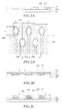
- FIGS. 1A-1E are cross-sectional views illustrating a method for fabricating a packaging substrate 1 according to the prior art.
- a substrate body 10 covered by an insulating protective layer 11 is provided, the substrate body 10 has a plurality of conductive pads 100 disposed on a surface thereof, and the insulating protective layer 11 is utilized as a solder mask and has a plurality of openings 110 such that a portion of end surfaces of the conductive pads 100 are exposed by the openings 110 , causing the conductive pads 100 to be solder-mask-defined (SMD).
- SMD solder-mask-defined
- the substrate body 10 includes a dielectric layer 10 b and a circuit layer 10 a disposed on the dielectric layer 10 b (as shown in FIG. 1 A′).
- the circuit layer 10 a has a plurality of conductive traces 101 and the conductive pads 100 connected to the conductive traces 101 .
- the end surfaces of the conductive pads 100 are round, and the openings 110 are also round.
- openings 110 of the insulating protective layer 11 can also expose all end surfaces of the conductive pads 100 ′ such that the conductive pads 100 ′ are non-solder-mask-defined.
- FIG. 1B shows a subsequent process of FIGS. 1 A and 1 A′.
- a resist layer 12 is formed on the insulating protective layer 11 , and has a plurality of openings 120 exposing the conductive pads 100 by exposure and development methods.
- a diameter w of the opening 120 is bigger than a diameter v of the opening 110 .
- copper bumps 13 are formed by electroplating on the openings 120 such that the conductive pads 100 are electrically connected to the copper bumps 13 .
- the resist layer 12 is removed.
- a solder bump 15 is formed on the copper bump 13 to cover the copper bump 13 .
- the uneven thermal stress may easily cause a crack c at the insulating protective layer 11 under the wing structure 130 , as shown in FIG. 1D .
- the crack c not only reduces the reliability of the packaging substrate 1 , but also causes the failure of test for the packaging substrate 1 .
- the diameter v of the opening 110 is less than the greatest diameter of the copper bump 13 (as the diameter w of the wing structure 130 ) such that the diameter v of the opening 110 may not equal to the greatest diameter of the copper bump 13 , as shown in FIG. 1D . Therefore, the reliability of the copper bump 13 cannot be enhanced so that a solder ball may be left off during the push-pull bond test for the solder bump 15 .
- the spacing S between the conductive pad 100 and the conductive traces 101 directly effects the yield. If the spacing S is small, the yield of a circuit is low. However, in the conventional packaging substrate 1 , the yield cannot be promoted due to the fact that the spacing S cannot be increased any further.
- the present invention provides a packaging substrate, comprising: a substrate body having a plurality of conductive pads disposed on a surface thereof; an insulating protective layer formed on the surface of the substrate body and having openings for the conductive pads to be exposed therefrom; and conductive pillars disposed on end surfaces of the conductive pads exposed from the openings and having first ends and opposite second ends, therewith the first ends being closer than the second ends from the conductive pads, and the first ends having a width bigger than a width of the second ends.
- the openings are round, and each of the end surfaces of the conductive pads has a length and a width less than the length, and are oval or rectangular.
- a non-solder-mask-defined (NSMD) type is designed in the width direction of the end surface between the insulating protective layer and the conductive pad
- a solder-mask-defined (SMD) type is designed in the length direction of the end surface. That is, to replace a portion of a design of the conventional SMD with a design of the NSMD, so the spacing between the conductive pad and the conductive trace can be increased thereby to raise the density of wiring layout on the substrate body surface or therefore to promote the flexibility of wiring layout.
- the conductive pad is disposed on the surface of the substrate body or embedded in the substrate body to expose the end surface on the substrate body.
- the conductive pad is solder-mask-defined (SMD) or non-solder-mask-defined (NSMD).
- SMD solder-mask-defined
- NSMD non-solder-mask-defined
- the end surface width is non-solder-mask-defined and the end surface length is solder-mask-defined. Therefore, in comparison with conventional NSMD design, the present invention covers the dielectric surface of the substrate body by forming the conductive pillars in the openings, and increases the bonding ability to the conductive pad.
- the conductive pad is located on the substrate body, the opening does not penetrate the insulating protective layer, and the bottom surface of the opening of the insulating protective layer is lower than or flush with the surface of the conductive pad.
- the first end of the conductive pillar is in contact with the conductive pad.
- the conductive pillar further has a seat body in the opening, and the seat body extends from the first end of the conductive pillar and is in contact with the conductive pad.
- the surface of the seat body is lower than or flush with the rim of the opening.
- the width of the seat body is bigger than, less than or equal to the width of the first end.
- the conductive pillar further has a lateral surface between the first end and the second end, and the lateral surface is a flat or arced.
- the packaging substrate further comprises metal pillars disposed on the substrate body and surrounding the conductive pillars, and the metal pillar has a first segment and a second segment.
- the first segment of the metal pillar and the conductive pillar have similar structures.
- the packaging substrate according to the present invention has a conductive pillar, in which the first end is wider than the second end so that the conductive pillar does not form a wing structure, and therefore spacing between contacts can be decreased to satisfy the demands for fine-pitch and multi-joints.
- the conductive pillar does not form a wing structure, there is no metal material on the insulating protective layer during the performance of temperature cycling test (TCT).
- TCT temperature cycling test
- the conductive pillar forms a cone-shaped structure so that the diameter of the opening is equal to the greatest diameter of the conductive pillar (as the first end).
- the reliability of the conductive pillar can therefore be enhanced to avoid a solder ball to be left off during the performance of the push-pull bond test.
- the cone-shaped structure of the conductive pillar increases the surface areas such that that the adhesion areas between the conductive pillar and a solder material can be increased to enhance the bonding ability between the conductive pillar and a solder material.
- FIGS. 1A-1E are cross-sectional views of a method for fabricating a packaging substrate according to the prior art, wherein FIG. 1 A′ is a local top view of FIG. 1A , and FIG. 1 A′′ is another pattern of FIG. 1 A′;
- FIGS. 2A-2F are cross-sectional views of a method for fabricating a packaging substrate according the present invention, wherein FIG. 2 A′ is a local top view of another embodiment of FIG. 2A , FIGS. 2 D′ and 2 D′′ are yet another embodiments of FIG. 2D , FIGS. 2 E′, 2 F and 2 F′ are further another embodiments of FIG. 2E ;
- FIGS. 3A-3E are cross-sectional views of various patterns of a first embodiment of a method for fabricating a packaging substrate according to the present invention.
- FIGS. 4A-4E are cross-sectional views of patterns of a second embodiment of a method for fabricating a packaging substrate according to the present invention.
- FIGS. 5A-5E are cross-sectional views of patterns of a third embodiment of a method for fabricating a packaging substrate according to the present invention.
- FIGS. 6A-6E are cross-sectional views of patterns of a fourth embodiment of a method for fabricating a packaging substrate according to the present invention.
- FIGS. 7A-7E are cross-sectional views of patterns of a fifth embodiment of a method for fabricating a packaging substrate according to the present invention.
- FIGS. 8A-8E are cross-sectional views of patterns of a sixth embodiment of a method for fabricating a packaging substrate according to the present invention.
- FIGS. 2A-2F are cross-sectional views of a method for fabricating a packaging substrate according to the present invention.
- a substrate body 20 having a plurality of conductive pads 200 is provided, and an insulating protective layer 21 is formed on the surface of substrate body 20 and the conductive pads 200 .
- the insulating protective layer 21 also has a plurality of openings such that a portion of end surfaces of the conductive pads 200 is exposed from the openings 210 , causing the conductive pads 200 to be solder-mask-defined (SMD).
- SMD solder-mask-defined
- the substrate body 20 has a dielectric layer, and a circuit layer 20 a is formed on the dielectric layer.
- the circuit layer 20 a has a plurality of conductive traces 201 (as shown in FIG. 2 A′) and the conductive pads 200 connected to the conductive traces 201 . That is, the conductive pads 200 are disposed on the dielectric layer of the substrate body.
- the end surface of the conductive pad 200 is round, and the opening 210 is also round.
- the length Y of the end surface is bigger than the width X of the end surface of the conductive pad 200 ′ such that the end surface of the conductive pad 200 ′ is preferably oval or rectangular (not illustrated).
- a non-solder-mask-defined (NSMD) type is designed in the axial direction of the width X of the end surface
- a solder-mask-defined (SMD) type is designed in the direction of the length Y of the end surface. That is, to replace a portion of a design of the conventional SMD with a design of the NSMD, so the spacing S′ between the conductive pad 200 ′ and the conductive trace 201 can be increased to raise the density of wiring layout on the surface of the substrate body 20 or therefore to promote the flexibility of wiring layout.
- the length Y of the end surface of the conductive pad 200 ′ is, for example, 80 ⁇ m
- the width X of the end surface is, for example, 40 ⁇ m
- the diameter of the opening 210 is, for example, 60 ⁇ m such that the spacing z between the conductive pad 200 ′ and the opening 210 is, for example, 10 ⁇ m.
- the spacing b between the opening 210 and the conductive trace 201 is, for example, 13 ⁇ m
- the trace width a of the conductive trace 201 is, for example, 14 ⁇ m
- the spacing between the conductive pads 200 ′ is, for example, 100 ⁇ m.
- FIG. 2B shows a subsequent process of FIG. 2A .
- a conductive seedlayer 23 ′′ is formed on the insulating protective layer 21 and the conductive pads 200 to thereby form a metal layer 23 ′ by electroplating.
- a resist layer 22 is formed on the metal layer 23 ′, and the resist layer 22 has a patterned open region 220 formed to expose the metal layer 23 ′ such that the remaining resist layer 22 covers the metal layer 23 ′ on the conductive pads 200 .
- a photo-resist layer it is not limited to use a photo-resist layer, and is not limited by the lithography machine, so the limitation that alligning accuracy should be less than or equal to, for example, 12.5 ⁇ m may be eliminated.
- the metal layer 23 ′ in the patterned open region 220 is removed by etching, and the remained metal layer 23 ′ serves as the conductive pillar 23 .
- the conductive pillar 23 is a copper pillar and disposed on the conductive pad 200 , and the conductive pillar 23 has opposite first end 23 a and second end 23 b .
- the first end 23 a is closer to the conductive pad 200 than the second end 23 b.
- the conductive pillar 23 further has a seat body 230 in the opening 210 , and the seat body 230 is located between the conductive pad 200 and the first end 23 a.
- a resist layer 22 is removed to expose the second end 23 b of the conductive pillar 23 provided for bonding a semiconductor chip (not illustrated).
- the periphery of the substrate body 20 further has a plurality of conductive pads 202 , and correspondingly a plurality of metal pillars 26 such as copper pillars disposed on the conductive pads 202 to surround the conductive pillars, and thus provided to stack and bond a package (not illustrated) to form package on package (POP).
- a package not illustrated
- POP package on package
- the conductive pillars 23 may be formed first, and the metal pillars 26 are formed by electroplating. Alternatively, the conductive pillars 23 and the first segments 261 of the metal pillars 26 ′ may be formed simultaneously, then the second segments 262 of the metal pillars 26 ′ are formed thereafter, as shown in FIG. 2 D′′. Therefore, the first segments 261 of the metal pillars 26 ′ and the conductive pillars 23 have similar structures such as a cone-shaped structure.
- a surface finish layer 24 is formed on the conductive pillars 23 in a subsequent process, and is then covered by a solder material 25 .
- a material forming the surface finish layer 24 is one selected from the group consisting of electroplated nickel/gold, electroless plated nickel/gold, electroless nickel immersion gold (ENIG), electroless nickel electroless palladium immersion gold (ENEPIG), immersion tin and organic solderability preservative (OSP).
- solder material 25 can be formed by electroplating, electroless plating, hot air solder leveling (HASL), or printing such as stencil printing or dry film printing.
- HASL hot air solder leveling
- a surface finish layer 24 or a solder material 25 may also be formed on the metal pillars 26 , 26 ′.
- FIG. 2 E′ is a subsequent process of FIG. 2 A′.
- the surface finish layer 24 is formed both on the metal pillar 26 , 26 ′ and the conductive pillar 23 , and the surface finish layer 24 both on the conductive pillar 23 and the metal pillar 26 , 26 ′ are covered by the solder material 25 , as shown in FIG. 2F .
- the surface finish layer 24 is formed both on the metal pillar 26 , 26 ′ and the conductive pillar 23 , while the solder material 25 is not formed on the surface finish layer 24 on the metal pillar 26 , 26 ′, as shown in FIG. 2 F′.
- metal layer etching is utilized such that the width d of the first end 23 a (the lower end) is bigger than the width r of the second end 23 b (the upper end) of the conductive pillar 23 . Therefore, the conductive pillar does not form a wing structure, and the spacing P′ between the solder material 25 can be reduced to be equal to or less than, for example, 130 ⁇ m, as shown in FIG. 2E , to satisfy demands for fine-pitch and multi-joints.
- the conductive pillar 23 does not form a wing structure, there is no metal material on the insulating protective layer 11 during the performance of temperature cycling test (TCT). The crack is hence avoided. Therefore, the reliability of the packaging substrate 2 is improved, and the successful test of the packaging substrate 2 can be expected.
- TCT temperature cycling test
- the conductive pillar 23 forms a cone-shaped structure such that the rim diameter of the opening 210 is equal to the greatest diameter of the conductive pillar 23 (for example, the width d of the first end 23 a of the conductive pillar 23 ) as shown in FIG. 2D .
- the reliability of the conductive pillar 23 can therefore be enhanced, and a solder ball can be avoided to be left off during the performance of the push-pull bond test for the joint structure consisting of the solder material 25 and the conductive pillar 23 .
- the cone-shaped structure of the conductive pillar 23 has more surface areas. Therefore, the adhesion areas of the conductive pillar 23 and the solder material 25 are increased, and the bonding ability between the conductive pillar 23 and the solder material 25 is thus enhanced.
- FIGS. 3A-3E are various patterns of a first embodiment for the packaging substrate according to the present invention.
- the conductive pad 200 is disposed on the substrate body 20 , and the opening 210 of the insulating protective layer 21 exposes a portion of surface of the conductive pad 200 such that the conductive pad 200 is SMD-type.
- the first end 33 a of the conductive pillar 33 is in contact with the conductive pad 200 , and the conductive pillar 33 further has a lateral surface 33 c between the first end 33 a and the second end 33 b .
- the lateral surface 33 c is an arced surface such as a concave face, and the solder material 25 covers the conductive pillar 33 .
- the conductive pillar 33 ′ has a seat body 330 in the opening 210 .
- the seat body 330 extends from the first end 33 a of the conductive pillar 33 ′ and is in contact with the conductive pad 200 , and the height t of the seat body 330 is less than the height h of the opening 210 .
- the height t′ of the seat body 330 ′ is equal to the height h of the opening 210
- the width m of the seat body 330 ′ is equal to the width n of the first end 33 a .
- the process of FIG. 3C may refers to the process of FIG. 2D .
- the width m of the seat body 330 ′ is less than the width n′ of the first end 33 a ′. That is, the first end 33 a ′ of the conductive pillar 33 ′ is partially located on the insulating protective layer 21 .
- the metal material bonded to the surface on the insulating protective layer 21 is not sufficient to influence results of contact pitch, temperature cycling test and push-pull bond test since the conductive pillar 33 ′ has a structure tapered upward.
- the lateral surface 33 c ′ of the conductive pillar 33 ′ is flat.
- the width of the seat body 330 may be bigger than the width of the first end 33 a (not illustrated).
- FIGS. 4A-4E show a second embodiment of the packaging substrate of the present invention.
- the second embodiment differs from the first embodiment in that the conductive pad 400 of the second embodiment is non-solder-mask-defined (NSMD), and the rest structures in FIGS. 4A-4E correspond to the rest structures in FIGS. 3A-3E .
- NSMD non-solder-mask-defined
- the opening 210 of the insulating protective layer 21 exposes the entire surface of the conductive pad 400 and dielectric materials around (as the substrate body 20 surface) such that the conductive pillar 43 (or the seat body 430 , 430 ′ of the conductive pillar 43 ′) wraps the conductive pad 400 , and the solder material 25 covers the conductive pillar 43 ′.
- FIGS. 5A-5E show a third embodiment of a packaging substrate according to the present invention.
- the third embodiment differs from the first embodiment in that the conductive pad 500 of the third embodiment is embedded in the substrate body 20 and exposes the end surface thereof on the substrate body 20 surface, and the rest structures (such as the conductive pillar 53 , 53 ′) in FIGS. 5A-5E correspond to the rest structures (such as the conductive pillar 33 , 33 ′) in FIGS. 3A-3E .
- the rest structures such as the conductive pillar 53 , 53 ′
- FIGS. 5A-5E correspond to the rest structures (such as the conductive pillar 33 , 33 ′) in FIGS. 3A-3E .
- the same parts are therefore not specified again.
- FIGS. 6A-6E show a fourth embodiment of a packaging substrate according to the present invention.
- the fourth embodiment differs from the second embodiment in that the conductive pad 600 is embedded in the substrate body 20 and exposes the end surface thereof on the substrate body 20 surface, and the rest structures (such as the conductive pillar 63 , 63 ′) in FIGS. 6A-6E correspond to the rest structures (such as the conductive pillar 43 , 43 ′) in FIGS. 4A-4E .
- the rest structures such as the conductive pillar 63 , 63 ′
- FIGS. 6A-6E correspond to the rest structures (such as the conductive pillar 43 , 43 ′) in FIGS. 4A-4E .
- the same parts are therefore not specified again.
- FIGS. 7A-7E show a fifth embodiment of a packaging substrate according to the present invention.
- the fifth embodiment differs from the second embodiment mainly in that the opening 710 of the fifth embodiment is ‘recess’-like so does not penetrate the insulate protection layer 71 , and the rest structures (such as the conductive pillar 73 , 73 ′) in FIGS. 7A-7E correspond to the rest structures (such as the conductive pillar 43 , 43 ′) in FIGS. 4A-4E .
- the same parts are therefore not specified again.
- the substrate is NSMD design, and the bottom face of the opening 710 of the insulating protective layer 71 is lower than the conductive pad surface 700 , a height difference k is therefore generated so that the conductive pad 700 protrudes the bottom face of the opening 710 of the insulating protective layer 71 .
- FIGS. 8A-8E show a sixth embodiment of a packaging substrate according to the present invention.
- the sixth embodiment differs from the fifth embodiment in that the bottom face of the opening 810 of the insulating protective layer 81 of the sixth embodiment is flush with the conductive pad surface 800 , and the rest structures (such as the conductive pillar 83 , 83 ′) in FIGS. 8A-8E correspond to the rest structures (such as the conductive pillar 73 , 73 ′) in FIGS. 7A-7E .
- the rest structures such as the conductive pillar 83 , 83 ′
- FIGS. 8A-8E correspond to the rest structures (such as the conductive pillar 73 , 73 ′) in FIGS. 7A-7E .
- the same parts are therefore not specified again.
- the conductive pillar being higher than the insulating protective layer facilitates the subsequent process of forming the solder material and the promotion of the yield thereof.
- the first end of the conductive pillar is lower than the rim of the opening.
- the seventh to tenth embodiments may be obtained by incorporating the structure of FIG. 2 A′ in the first to sixth embodiments.
- the seventh embodiment corresponds the length Y of the end surface of the conductive pad 200 ′ to the structure of the first embodiment (as FIGS. 3A-3E ), and corresponds the width X of the end surface of the conductive pad 200 ′ to the structure of the second embodiment (as FIG. 4 A′ and FIGS. 4B-4E ).
- the eighth embodiment corresponds the length Y of the end surface of the conductive pad 200 ′ to the structure of the third embodiment (as FIGS. 5A-5E ), and corresponds the width X of the end surface of the conductive pad 200 ′ to the structure of the fourth embodiment (as FIGS. 6A-6E ).
- the ninth embodiment corresponds the width X of the end surface of the conductive pad 200 ′ to the structure of the fifth embodiment (as FIGS. 7A-7E ).
- the tenth embodiment corresponds the width X of the end surface of the conductive pad 200 ′ to the structure of the sixth embodiment (as FIGS. 8A-8E ).
- the first end of The surface of The surface of the conductive the seat body of the seat body of pillar is bigger
- the lateral the conductive the conductive than the width of surface of the Conductive pillar is lower pillar is flush the seat body conductive pillar has no than the rim of with the rim of (the rim of pillar is a seat body the opening the opening the opening) flat bevel.
- circuit is on the FIG. 3A FIG. 3B FIG. 3C FIG. 3D
- FIG. 3E dielectric layer (SMD) circuit is on the FIG. 4A FIG. 4B FIG. 4C FIG. 4D
- FIG. 4E dielectric layer (NSMD) circuit is buried in FIG. 5A FIG. 5B FIG. 5C FIG. 5D FIG.
- FIG. 5E the dielectric layer (SMD) circuit is buried in FIG. 6A FIG. 6B FIG. 6C FIG. 6D
- FIG. 6E the dielectric layer (NSMD) opening bottom is FIG. 7A FIG. 7B FIG. 7C FIG. 7D FIG. 7E lower than the pad surface (NSMD) opening bottom is FIG. 8A FIG. 8B FIG. 8C FIG. 8D FIG. 8E flush with the pad surface (NSMD)
- the present invention also provides a packaging substrate 2 , 2 ′, comprising: a substrate body 20 having a plurality of conductive pads 200 , 200 ′ disposed on a surface thereof; an insulating protective layer 21 formed on the substrate body 20 ; and conductive pillars 23 disposed on surfaces of the conductive pads 200 .
- the insulating protective layer 21 has a plurality of openings for conductive pads 200 , 200 ′ to be exposed therefrom, and the opening 210 is preferably round.
- the conductive pillar 23 has the first end 23 a opposite to the second end 23 b .
- the first end 23 a is closer to the conductive pad 200 than the second end 23 b , and the width d of the first end 23 a is bigger than the width r of the second end 23 b.
- the length Y of the end surface of the conductive pad 200 ′ is bigger than the width X of the end surface of the conductive pad 200 ′ such that the end surface of the conductive pad 200 ′ is preferably oval or rectangular.
- the conductive pad 200 , 400 is disposed on a surface of the substrate body 20 .
- the conductive pad 500 , 600 is embedded in the substrate body 20 to expose the end surface on the surface of the substrate body 20 .
- the conductive pad 200 is solder-mask-defined (SMD).
- the conductive pad 500 , 600 is non-solder-mask-defined (NSMD).
- the conductive pad 200 ′ performs a non-solder-mask-defined (NSMD) type in the direction of the end surface width, and performs a solder-mask-defined (SMD) type in the direction of the end surface length.
- NSMD non-solder-mask-defined
- SMD solder-mask-defined
- the conductive pad 700 , 800 is located on the substrate body 20 , the opening 710 , 810 is ‘recess’-like so does not penetrate the insulating protective layer 71 , 81 , and the bottom surface of the opening 710 of the insulating protective layer 71 is lower than the conductive pad surface 700 .
- the bottom surface of the opening 810 of the insulating protective layer 81 is flush with the conductive pad surface 800
- the pillar 23 , 33 , 33 ′ further has a lateral surface 33 c , 33 c ′ between the first end 23 a , 33 a , 33 a ′ and the second end 23 b , 33 b , and the lateral surface 33 c is an arced surface or a flat surface.
- the first end 33 a of the conductive pillar 33 is in contact with the conductive pad 200 .
- the conductive pillar 23 , 33 ′ further has a seat body 230 , 330 , 330 ′ in the opening 210 .
- the seat body 230 , 330 , 330 ′ extends from the first end 23 a , 33 a , 33 a ′ of the conductive pillar 23 , 33 ′ and is in contact with the conductive pad 200 .
- the height t of the seat body 330 is less than the rim height h of the opening 210 .
- the height t′ of the seat body 330 ′ is equal to the rim height h of the opening 210 .
- the width m of the seat body 330 ′ is less than the width n of the first end 33 a .
- the width m of the seat body 330 ′ is equal to the width n′ of the first end 33 a ′, or the width m (not illustrated) of the seat body 330 ′ is bigger than the width of the first end.
- a metal pillars 26 , 26 ′ is further disposed on the substrate body 20 to surround the conductive pillars 23 .
- the metal pillar 26 ′ has the first segment 261 and the second segment 262 , and the first segment 261 of the metal pillar 26 ′ and the conductive pillar 23 have similar structures.
- the packaging substrate according to the present invention utilizes that the width of the first end is bigger than the width of the second to form a structure without a wing structure to reduce the distance between contact points and satisfy the demands for fine-pitch and multi-joints.
- the conductive pillar does not form a wing structure, the crack of the insulating protective layer, while the temperature cycling test is performed, is therefore avoided, and the reliability of the packaging substrate is improved.
- the conductive pillar forms a cone-shaped structure such that the diameter of the opening is equal to the width of the first end of the conductive pillar. Therefore the reliability of the conductive pillar can be enhanced to avoid the issue of leaving solder balls.
- the cone-shaped structure of the conductive pillar increases the adhesion areas between the conductive pillar and a solder material to enhance the bonding ability between both two.
Abstract
Description
| The first end of | ||||||
| The surface of | The surface of | the conductive | ||||
| the seat body of | the seat body of | pillar is bigger | The lateral | |||
| the conductive | the conductive | than the width of | surface of the | |||
| Conductive | pillar is lower | pillar is flush | the seat body | conductive | ||
| pillar has no | than the rim of | with the rim of | (the rim of | pillar is a | ||
| seat body | the opening | the opening | the opening) | flat bevel. | ||
| circuit is on the | FIG. 3A | FIG. 3B | FIG. 3C | FIG. 3D | FIG. 3E |
| dielectric layer | |||||
| (SMD) | |||||
| circuit is on the | FIG. 4A | FIG. 4B | FIG. 4C | FIG. 4D | FIG. 4E |
| dielectric layer | |||||
| (NSMD) | |||||
| circuit is buried in | FIG. 5A | FIG. 5B | FIG. 5C | FIG. 5D | FIG. 5E |
| the dielectric | |||||
| layer (SMD) | |||||
| circuit is buried in | FIG. 6A | FIG. 6B | FIG. 6C | FIG. 6D | FIG. 6E |
| the dielectric | |||||
| layer (NSMD) | |||||
| opening bottom is | FIG. 7A | FIG. 7B | FIG. 7C | FIG. 7D | FIG. 7E |
| lower than the pad | |||||
| surface (NSMD) | |||||
| opening bottom is | FIG. 8A | FIG. 8B | FIG. 8C | FIG. 8D | FIG. 8E |
| flush with the pad | |||||
| surface (NSMD) | |||||
Claims (19)
Priority Applications (1)
| Application Number | Priority Date | Filing Date | Title |
|---|---|---|---|
| US14/174,858 US9408313B2 (en) | 2012-12-28 | 2014-02-07 | Packaging substrate and method of fabricating the same |
Applications Claiming Priority (3)
| Application Number | Priority Date | Filing Date | Title |
|---|---|---|---|
| TW101225514 | 2012-12-28 | ||
| TW101225514U | 2012-12-28 | ||
| TW101225514U TWM459517U (en) | 2012-12-28 | 2012-12-28 | Package substrate |
Related Child Applications (1)
| Application Number | Title | Priority Date | Filing Date |
|---|---|---|---|
| US14/174,858 Continuation-In-Part US9408313B2 (en) | 2012-12-28 | 2014-02-07 | Packaging substrate and method of fabricating the same |
Publications (2)
| Publication Number | Publication Date |
|---|---|
| US20140182912A1 US20140182912A1 (en) | 2014-07-03 |
| US9111818B2 true US9111818B2 (en) | 2015-08-18 |
Family
ID=49481085
Family Applications (1)
| Application Number | Title | Priority Date | Filing Date |
|---|---|---|---|
| US14/018,757 Expired - Fee Related US9111818B2 (en) | 2012-12-28 | 2013-09-05 | Packaging substrate |
Country Status (2)
| Country | Link |
|---|---|
| US (1) | US9111818B2 (en) |
| TW (1) | TWM459517U (en) |
Cited By (2)
| Publication number | Priority date | Publication date | Assignee | Title |
|---|---|---|---|---|
| USRE45932E1 (en) * | 2008-03-06 | 2016-03-15 | Ps4 Luxco S.A.R.L. | Semiconductor device and method of manufacturing the same |
| US10897820B2 (en) * | 2016-09-01 | 2021-01-19 | Canon Kabushiki Kaisha | Printed wiring board, printed circuit board, and electronic device |
Families Citing this family (14)
| Publication number | Priority date | Publication date | Assignee | Title |
|---|---|---|---|---|
| US10833033B2 (en) * | 2011-07-27 | 2020-11-10 | Taiwan Semiconductor Manufacturing Co., Ltd. | Bump structure having a side recess and semiconductor structure including the same |
| TWI548011B (en) * | 2014-05-13 | 2016-09-01 | 矽品精密工業股份有限公司 | Package substrates and methods for fabricating the same |
| US10468363B2 (en) | 2015-08-10 | 2019-11-05 | X-Celeprint Limited | Chiplets with connection posts |
| TWI562256B (en) * | 2015-09-07 | 2016-12-11 | Siliconware Precision Industries Co Ltd | Substrate structure |
| TWI585925B (en) * | 2016-02-05 | 2017-06-01 | 矽品精密工業股份有限公司 | Substrate structure |
| DE102016103585B4 (en) * | 2016-02-29 | 2022-01-13 | Infineon Technologies Ag | Process for manufacturing a package with solderable electrical contact |
| US10103069B2 (en) | 2016-04-01 | 2018-10-16 | X-Celeprint Limited | Pressure-activated electrical interconnection by micro-transfer printing |
| DE102016107792B4 (en) * | 2016-04-27 | 2022-01-27 | Infineon Technologies Ag | Pack and semi-finished product with a vertical connection between support and bracket and method of making a pack and a batch of packs |
| TWI577248B (en) * | 2016-07-19 | 2017-04-01 | 欣興電子股份有限公司 | Circuit carrier and manufacturing mtheod thereof |
| US10222698B2 (en) | 2016-07-28 | 2019-03-05 | X-Celeprint Limited | Chiplets with wicking posts |
| US11064609B2 (en) | 2016-08-04 | 2021-07-13 | X Display Company Technology Limited | Printable 3D electronic structure |
| US10115692B2 (en) | 2016-09-14 | 2018-10-30 | International Business Machines Corporation | Method of forming solder bumps |
| US10276480B1 (en) * | 2017-10-26 | 2019-04-30 | Advanced Semiconductor Engineering, Inc. | Semiconductor structure |
| JP2021093431A (en) * | 2019-12-10 | 2021-06-17 | イビデン株式会社 | Printed wiring board and manufacturing method of printed wiring board |
Citations (1)
| Publication number | Priority date | Publication date | Assignee | Title |
|---|---|---|---|---|
| US20080253097A1 (en) * | 2007-04-10 | 2008-10-16 | Ibiden Co., Ltd | Interposer |
-
2012
- 2012-12-28 TW TW101225514U patent/TWM459517U/en not_active IP Right Cessation
-
2013
- 2013-09-05 US US14/018,757 patent/US9111818B2/en not_active Expired - Fee Related
Patent Citations (1)
| Publication number | Priority date | Publication date | Assignee | Title |
|---|---|---|---|---|
| US20080253097A1 (en) * | 2007-04-10 | 2008-10-16 | Ibiden Co., Ltd | Interposer |
Cited By (2)
| Publication number | Priority date | Publication date | Assignee | Title |
|---|---|---|---|---|
| USRE45932E1 (en) * | 2008-03-06 | 2016-03-15 | Ps4 Luxco S.A.R.L. | Semiconductor device and method of manufacturing the same |
| US10897820B2 (en) * | 2016-09-01 | 2021-01-19 | Canon Kabushiki Kaisha | Printed wiring board, printed circuit board, and electronic device |
Also Published As
| Publication number | Publication date |
|---|---|
| US20140182912A1 (en) | 2014-07-03 |
| TWM459517U (en) | 2013-08-11 |
Similar Documents
| Publication | Publication Date | Title |
|---|---|---|
| US9111818B2 (en) | Packaging substrate | |
| US10930625B2 (en) | Semiconductor package and method of fabricating the same | |
| KR101548428B1 (en) | Package having substrate with embedded metal trace overlapped by landing pad | |
| US20120267779A1 (en) | Semiconductor package | |
| US20080142993A1 (en) | Flip-chip mounting substrate | |
| US20130249083A1 (en) | Packaging substrate | |
| US20080265411A1 (en) | Structure of packaging substrate and method for making the same | |
| TWI397358B (en) | Wire bonding substrate and fabrication thereof | |
| US20090102050A1 (en) | Solder ball disposing surface structure of package substrate | |
| US20130334684A1 (en) | Substrate structure and package structure | |
| US7554197B2 (en) | High frequency IC package and method for fabricating the same | |
| JP2009194079A (en) | Wiring substrate for use in semiconductor apparatus, method for fabricating the same, and semiconductor apparatus using the same | |
| TWI636536B (en) | Semiconductor package | |
| US20070111499A1 (en) | Wafer redistribution structure with metallic pillar and method for fabricating the same | |
| JP4494249B2 (en) | Semiconductor device | |
| US9559076B2 (en) | Package having substrate with embedded metal trace overlapped by landing pad | |
| TWI646639B (en) | Semiconductor package | |
| US9408313B2 (en) | Packaging substrate and method of fabricating the same | |
| JP2014504034A (en) | Electronic device tape with enhanced lead cracks | |
| JP2010232616A (en) | Semiconductor device, and wiring board | |
| US20060252249A1 (en) | Solder ball pad surface finish structure of circuit board and fabrication method thereof | |
| KR102633431B1 (en) | Semiconductor device and manufacturing method thereof | |
| KR20110017153A (en) | Ball grid array(bga) package board and method for manufacturing the same | |
| TWI575619B (en) | Semiconductor package structure and manufacturing method thereof | |
| US11670574B2 (en) | Semiconductor device |
Legal Events
| Date | Code | Title | Description |
|---|---|---|---|
| AS | Assignment |
Owner name: UNIMICRON TECHNOLOGY CORPORATION, TAIWAN Free format text: ASSIGNMENT OF ASSIGNORS INTEREST;ASSIGNORS:LIN, CHUN-TING;HSIEH, YU-CHUNG;WANG, YING-TUNG;AND OTHERS;REEL/FRAME:031143/0224 Effective date: 20130523 |
|
| STCF | Information on status: patent grant |
Free format text: PATENTED CASE |
|
| FEPP | Fee payment procedure |
Free format text: MAINTENANCE FEE REMINDER MAILED (ORIGINAL EVENT CODE: REM.); ENTITY STATUS OF PATENT OWNER: LARGE ENTITY |
|
| LAPS | Lapse for failure to pay maintenance fees |
Free format text: PATENT EXPIRED FOR FAILURE TO PAY MAINTENANCE FEES (ORIGINAL EVENT CODE: EXP.); ENTITY STATUS OF PATENT OWNER: LARGE ENTITY |
|
| STCH | Information on status: patent discontinuation |
Free format text: PATENT EXPIRED DUE TO NONPAYMENT OF MAINTENANCE FEES UNDER 37 CFR 1.362 |
|
| FP | Lapsed due to failure to pay maintenance fee |
Effective date: 20190818 |