US9082717B2 - Isolation region, semiconductor device and methods for forming the same - Google Patents

Isolation region, semiconductor device and methods for forming the same Download PDF

Info

Publication number
US9082717B2
US9082717B2 US13/119,129 US201113119129A US9082717B2 US 9082717 B2 US9082717 B2 US 9082717B2 US 201113119129 A US201113119129 A US 201113119129A US 9082717 B2 US9082717 B2 US 9082717B2
Authority
US
United States
Prior art keywords
semiconductor substrate
sidewall
isolation region
region
groove
Prior art date
Legal status (The legal status is an assumption and is not a legal conclusion. Google has not performed a legal analysis and makes no representation as to the accuracy of the status listed.)
Active, expires
Application number
US13/119,129
Other versions
US20120001198A1 (en
Inventor
Haizhou Yin
Huilong Zhu
Zhijiong Luo
Current Assignee (The listed assignees may be inaccurate. Google has not performed a legal analysis and makes no representation or warranty as to the accuracy of the list.)
Institute of Microelectronics of CAS
Original Assignee
Institute of Microelectronics of CAS
Priority date (The priority date is an assumption and is not a legal conclusion. Google has not performed a legal analysis and makes no representation as to the accuracy of the date listed.)
Filing date
Publication date
Application filed by Institute of Microelectronics of CAS filed Critical Institute of Microelectronics of CAS
Assigned to Institute of Microelectronics, Chinese Academy of Sciences reassignment Institute of Microelectronics, Chinese Academy of Sciences ASSIGNMENT OF ASSIGNORS INTEREST (SEE DOCUMENT FOR DETAILS). Assignors: ZHU, HUILONG, LUO, ZHIJIONG, YIN, HAIZHOU
Publication of US20120001198A1 publication Critical patent/US20120001198A1/en
Application granted granted Critical
Publication of US9082717B2 publication Critical patent/US9082717B2/en
Active legal-status Critical Current
Adjusted expiration legal-status Critical

Links

Images

Classifications

    • HELECTRICITY
    • H01ELECTRIC ELEMENTS
    • H01LSEMICONDUCTOR DEVICES NOT COVERED BY CLASS H10
    • H01L21/00Processes or apparatus adapted for the manufacture or treatment of semiconductor or solid state devices or of parts thereof
    • H01L21/02Manufacture or treatment of semiconductor devices or of parts thereof
    • H01L21/04Manufacture or treatment of semiconductor devices or of parts thereof the devices having potential barriers, e.g. a PN junction, depletion layer or carrier concentration layer
    • H01L21/18Manufacture or treatment of semiconductor devices or of parts thereof the devices having potential barriers, e.g. a PN junction, depletion layer or carrier concentration layer the devices having semiconductor bodies comprising elements of Group IV of the Periodic Table or AIIIBV compounds with or without impurities, e.g. doping materials
    • H01L21/30Treatment of semiconductor bodies using processes or apparatus not provided for in groups H01L21/20 - H01L21/26
    • H01L21/302Treatment of semiconductor bodies using processes or apparatus not provided for in groups H01L21/20 - H01L21/26 to change their surface-physical characteristics or shape, e.g. etching, polishing, cutting
    • H01L21/306Chemical or electrical treatment, e.g. electrolytic etching
    • H01L21/308Chemical or electrical treatment, e.g. electrolytic etching using masks
    • H01L21/3083Chemical or electrical treatment, e.g. electrolytic etching using masks characterised by their size, orientation, disposition, behaviour, shape, in horizontal or vertical plane
    • HELECTRICITY
    • H01ELECTRIC ELEMENTS
    • H01LSEMICONDUCTOR DEVICES NOT COVERED BY CLASS H10
    • H01L21/00Processes or apparatus adapted for the manufacture or treatment of semiconductor or solid state devices or of parts thereof
    • H01L21/70Manufacture or treatment of devices consisting of a plurality of solid state components formed in or on a common substrate or of parts thereof; Manufacture of integrated circuit devices or of parts thereof
    • H01L21/71Manufacture of specific parts of devices defined in group H01L21/70
    • H01L21/76Making of isolation regions between components
    • H01L21/762Dielectric regions, e.g. EPIC dielectric isolation, LOCOS; Trench refilling techniques, SOI technology, use of channel stoppers
    • H01L21/76224Dielectric regions, e.g. EPIC dielectric isolation, LOCOS; Trench refilling techniques, SOI technology, use of channel stoppers using trench refilling with dielectric materials
    • H01L21/76232Dielectric regions, e.g. EPIC dielectric isolation, LOCOS; Trench refilling techniques, SOI technology, use of channel stoppers using trench refilling with dielectric materials of trenches having a shape other than rectangular or V-shape, e.g. rounded corners, oblique or rounded trench walls
    • HELECTRICITY
    • H01ELECTRIC ELEMENTS
    • H01LSEMICONDUCTOR DEVICES NOT COVERED BY CLASS H10
    • H01L29/00Semiconductor devices specially adapted for rectifying, amplifying, oscillating or switching and having potential barriers; Capacitors or resistors having potential barriers, e.g. a PN-junction depletion layer or carrier concentration layer; Details of semiconductor bodies or of electrodes thereof ; Multistep manufacturing processes therefor
    • H01L29/66Types of semiconductor device ; Multistep manufacturing processes therefor
    • H01L29/66007Multistep manufacturing processes
    • H01L29/66075Multistep manufacturing processes of devices having semiconductor bodies comprising group 14 or group 13/15 materials
    • H01L29/66227Multistep manufacturing processes of devices having semiconductor bodies comprising group 14 or group 13/15 materials the devices being controllable only by the electric current supplied or the electric potential applied, to an electrode which does not carry the current to be rectified, amplified or switched, e.g. three-terminal devices
    • H01L29/66409Unipolar field-effect transistors
    • H01L29/66477Unipolar field-effect transistors with an insulated gate, i.e. MISFET
    • H01L29/66568Lateral single gate silicon transistors
    • H01L29/66636Lateral single gate silicon transistors with source or drain recessed by etching or first recessed by etching and then refilled
    • HELECTRICITY
    • H01ELECTRIC ELEMENTS
    • H01LSEMICONDUCTOR DEVICES NOT COVERED BY CLASS H10
    • H01L29/00Semiconductor devices specially adapted for rectifying, amplifying, oscillating or switching and having potential barriers; Capacitors or resistors having potential barriers, e.g. a PN-junction depletion layer or carrier concentration layer; Details of semiconductor bodies or of electrodes thereof ; Multistep manufacturing processes therefor
    • H01L29/66Types of semiconductor device ; Multistep manufacturing processes therefor
    • H01L29/68Types of semiconductor device ; Multistep manufacturing processes therefor controllable by only the electric current supplied, or only the electric potential applied, to an electrode which does not carry the current to be rectified, amplified or switched
    • H01L29/76Unipolar devices, e.g. field effect transistors
    • H01L29/772Field effect transistors
    • H01L29/78Field effect transistors with field effect produced by an insulated gate

Definitions

  • the present invention relates to a technical field of semiconductors, and particularly, to an isolation region, a semiconductor device and methods for forming the same.
  • a method for forming a semiconductor device comprises the following steps. Firstly, as illustrated in FIGS. 1 and 2 , an active region 20 and an isolation region 12 surrounding the active region 20 are formed on a semiconductor substrate 10 . Next, as illustrated in FIGS. 3 and 4 , a gate stack structure is formed on the active region 20 and extends to the isolation region 12 (the gate stack structure comprises a gate dielectric layer 22 , a gate 24 formed on the gate dielectric layer 22 , and sidewalls 26 surrounding the gate dielectric layer 22 and the gate 24 .
  • the gate stack structure comprises a gate dielectric layer 22 , a gate 24 formed on the gate dielectric layer 22 , and sidewalls 26 surrounding the gate dielectric layer 22 and the gate 24 .
  • a cap layer is further formed on the gate for preventing the gate from being damaged during the operation.
  • the cap layer is usually made of silicon nitride.
  • the cap layer is not indicated in the text and drawings of this specification for the convenience of description).
  • the gate stack structure and the isolation region 12 are used as a mask, and the semiconductor substrate 10 of a partial thickness in the active region 20 is removed to form a groove 30 .
  • a semiconductor material is produced in the groove 30 for filling into the groove 30 so as to form a source/drain (S/D) region.
  • a slot 34 is defined at an interface between the S/D region 32 and the isolation region 12 . Consequently, as illustrated in FIGS. 10 to 12 , when a contact region 36 (e.g., metal silicide layer) is formed subsequently on the S/D region 32 , the contact region 36 may likely reach a junction region via the slot 34 , thereby causing a leakage current.
  • a contact region 36 e.g., metal silicide layer
  • the present invention provides an isolation region, a semiconductor device and methods for forming the same, which are beneficial to reduce the leakage current.
  • the present invention provides an isolation region, comprising: a first groove and an insulation layer filling the first groove, wherein the first groove is embedded into a semiconductor substrate and comprises a first sidewall, a bottom surface and a second sidewall that extends from the bottom surface and joins to the first sidewall, and an angle between the first sidewall and a normal line of the semiconductor substrate is larger than a standard value.
  • the angle between the first sidewall and the normal line of the semiconductor substrate is in the range from about 5° to about 20° (5° ⁇ 20°.
  • the second sidewall is joined to the first sidewall at a first joint and a second joint, and an angle between the second sidewall and the normal line of the semiconductor substrate increases from the first joint to the second joint.
  • a semiconductor device comprising the above isolation region, the semiconductor device further comprises an S/D region, and the S/D region comprises a second groove and a semiconductor layer filling the second groove, wherein there is material of the semiconductor substrate interposed between the second groove and the first and second sidewalls.
  • the semiconductor layer is Si 1-x Ge x
  • the semiconductor layer is Si:C.
  • a method for forming an isolation region comprising: forming a first trench on a semiconductor substrate, wherein an angle between a sidewall of the first trench and a normal line of the semiconductor substrate is larger than a standard value; forming a mask on the sidewall to form a second trench on the semiconductor substrate by using the mask; and forming an insulation layer to fill the first and second trenches.
  • the angle between the sidewall and the normal line of the semiconductor substrate is about 5° ⁇ about 20°.
  • the method further comprises performing an etching operation on the second trench to expand the second trench.
  • a method for forming a semiconductor device comprising: forming the isolation region using the above method, so as to isolate active regions; forming on the semiconductor substrate a gate stack structure that resides on the active region and extends to the isolation region; using the gate stack structure and the isolation region as a mask to form a third trench in the active region, wherein there is material of the semiconductor substrate interposed between the third trench and the isolation region; and filling a semiconductor layer into the third trench to form an S/D region.
  • the semiconductor layer is Si 1-X Ge X
  • the semiconductor layer is Si:C.
  • the cross-sectional area of the embedded isolation region is made to be smaller than the opening area by increasing the angle between the first sidewall (i.e., the sidewall of the first trench) and the nominal line of the semiconductor substrate.
  • the S/D region is formed by using the opening of the isolation region as the mask.
  • an anisotropic etching process is adopted, so that the active region connected to the isolation region is removed at the opening of the isolation region.
  • each wall of the groove is made of the material of the semiconductor substrate (wherein, the sidewall of the groove close to the isolation region is made of the material of the semiconductor substrate, instead of the material of the isolation region, due to the material of the semiconductor substrate remaining between the groove and the isolation region).
  • the material of the semiconductor substrate is used as seed crystal to grow the material of the S/D region in the groove (when the material of the semiconductor substrate is Si, for a PMOS device, the semiconductor layer is Si 1-X Ge X , and for an NMOS device, the semiconductor layer is Si:C).
  • the semiconductor layer is Si 1-X Ge X , and for an NMOS device, the semiconductor layer is Si:C.
  • any cross-sectional plane perpendicular to the semiconductor substrate from the first joint to the second joint, the angle between the second sidewall and the normal line of the semiconductor substrate increases. This is beneficial to expand the cross-sectional area of a region defined by the second sidewall. Then, the above region is filled with the insulation layer to form the isolation region, and this is beneficial to enhance the isolation effect; or before the insulation layer is formed, an etching operation is performed on the second groove to expand the second groove, which may increase the cross-section area of the second groove. Then, the second groove is filled with the insulation layer, and this is beneficial to enhance the isolation effect.
  • FIGS. 1 ⁇ 2 illustrate structural diagrams after an active region is formed according to the prior art.
  • FIGS. 3 ⁇ 4 illustrate structural diagrams after a gate stack structure is formed according to the prior art.
  • FIGS. 5 ⁇ 6 illustrate structural diagrams after a groove is formed according to the prior art.
  • FIGS. 7 ⁇ 9 illustrate structural diagrams after an S/D region is formed according to the prior art.
  • FIGS. 10 ⁇ 12 illustrate structural diagrams after a contact region is formed according to the prior art.
  • FIG. 13 illustrates a structural diagram of a first embodiment of an isolation region according to the present invention.
  • FIG. 14 illustrates a structural diagram of a second embodiment of an isolation region according to the present invention.
  • FIG. 15 illustrates a structural diagram of an embodiment of a semiconductor device according to the present invention.
  • FIG. 16 illustrates a structural diagram after a first trench is formed in a first embodiment of a method for forming an isolation region according to the present invention.
  • FIG. 17 illustrates a structural diagram after a second trench is formed in the first embodiment of a method for forming an isolation region according to the present invention.
  • FIG. 18 illustrates a structural diagram after a second trench is formed in a second embodiment of a method for forming an isolation region according to the present invention.
  • FIG. 19 illustrates a structural diagram after an insulation layer is formed in the first embodiment of a method for forming an isolation region according to the present invention.
  • FIG. 20 illustrates a structural diagram after an isolation region is formed in an embodiment of a method for forming a semiconductor device according to the present invention.
  • FIG. 21 illustrates a structural diagram after a gate stack structure is formed in an embodiment of a method for forming a semiconductor device according to the present invention.
  • FIG. 22 illustrates a structural diagram after a third trench is formed in an embodiment of a method for forming a semiconductor device according to the present invention.
  • FIG. 23 illustrates a structural diagram after a semiconductor layer is formed in an embodiment of a method for forming a semiconductor device according to the present invention.
  • reference numbers and/or letters can be repeatedly used in different embodiments of the present invention for the purposes of simplification and clearness, without indicating the relationships between the discussed embodiments and/or arrangements.
  • the present invention provides an isolation region comprising a first groove 120 and an insulation layer 140 filling the first groove 120 .
  • the first groove 120 is embedded into a semiconductor substrate 100 and comprises a first sidewall 122 , a bottom surface 126 and a second sidewall 124 that extends from the bottom surface 126 and joins to the first sidewall 122 .
  • an angle between the first sidewall 122 and a normal line of the semiconductor substrate 100 is larger than a standard value.
  • the standard value means that when the groove 120 is to be etched in practice, if an angle between the sidewall of the groove 120 and the normal line of the semiconductor substrate 100 is designed to be ⁇ , while an angle actually obtained to meet the design requirement is ⁇ + ⁇ due to the demand of the process or procedure (e.g., there exists a process error or the subsequent filling effect needs to be improved), then ⁇ is a standard value.
  • the semiconductor substrate 100 is a substrate of silicon, and in other embodiments, the semiconductor substrate 100 may also be made of other compound semiconductor, such as silicon carbide (SiC), gallium arsenide (GaAs), indium arsenide (InAs) or indium phosphide (InP).
  • the semiconductor substrate 100 preferably includes an epitaxial layer.
  • the semiconductor substrate 100 may also include a silicon on insulator (SOI) structure.
  • SOI silicon on insulator
  • the insulation layer 140 may be made of silicon nitride, silicon oxynitride or non-doped silicon oxide.
  • the angle between the first sidewall 122 and the normal line of the semiconductor substrate 100 may be about 5° ⁇ about 20°, such as 8°, 10° or 15°.
  • the cross-sectional area of the embedded isolation region is made to be smaller than the opening area.
  • the material of the semiconductor substrate 100 may be residual between the groove bearing the material of an S/D region and the isolation region, i.e., each wall of the groove is made of the material of the semiconductor substrate 100 . This is beneficial to reduce the possibility of defining a slot at an interface between the formed S/D region and the isolation region.
  • the present invention further provides an isolation region.
  • the second sidewall 124 in any cross-sectional plane perpendicular to the semiconductor substrate 100 (for example, the cross-section as illustrated in FIG. 14 ), the second sidewall 124 is joined to the first sidewall 122 at a first joint 1224 and a second joint 1242 . From the first joint 1224 to the second joint 1242 , an angle between the second sidewall 124 and the normal line of the semiconductor substrate 100 increases. This is beneficial to expand a cross-sectional area of a region defined by the second sidewall 124 . Then, the above region is filled with the insulation layer 140 to form the isolation region, and this is beneficial to enhance the isolation effect.
  • the second sidewall 124 may have an arc shape, a fold line shape (not shown), etc.
  • the present invention provides a semiconductor device comprising the above isolation region (taking the second embodiment for example).
  • the semiconductor device further comprises a gate stack structure (the gate stack structure comprises a gate dielectric layer 102 , a gate 104 formed on the gate dielectric layer 102 , and sidewalls 106 surrounding the gate dielectric layer 102 and the gate 104 , which are beneficial to reduce a parasitic capacitance; and in other embodiments, the sidewalls 106 may be located on the gate dielectric layer 102 and surround the gate 104 ) and an S/D region (taking an embedded source/drain region for example).
  • the S/D region comprises a second groove 144 and a semiconductor layer 146 filling the second groove 144 .
  • the material of the semiconductor substrate 100 is interposed between the second groove 144 and the first and second sidewalls 122 , 124 (indicated by a dashed frame in the drawing). That is to say, when the second groove 144 bearing the material of the S/D region is formed, each wall of the second groove 144 is made of the material of the semiconductor substrate 100 , and then the material of the semiconductor substrate 100 is used as seed crystal. This is beneficial for a uniform growth of the semiconductor layer 146 for forming the S/D region along each direction in the second groove 144 , so as to reduce the possibility of defining a slot at an interface between the formed S/D region and the isolation region 142 .
  • the semiconductor layer may be Si 1-X Ge X (the value range of X may be about 0.1 ⁇ about 0.7, which can be flexibly adjusted according to a process requirement, such as 0.2, 0.3, 0.4, 0.5 or 0.6, and the value of X in this specification is the same as that indicated herein unless otherwise specified);
  • the semiconductor layer may be Si:C (the atomic percentage of C may be about 0.2% ⁇ about 2%, such as 0.5%, 1% or 1.5%, the content of C may be flexibly adjusted according to a process requirement, and the atomic percentage of C in this specification is the same as that indicated herein unless otherwise specified).
  • the semiconductor layer may be made of a semiconductor material doped with ions, e.g., Si 1-X Ge X or Si:C of N type or P type.
  • the ion doping operation may be performed directly during the production of the semiconductor material (e.g., adding a reactant containing the doped ion components into reactants for producing the semiconductor material), or performed through an ion implantation process after the semiconductor material is produced. Any conventional ion implantation process may be adopted to perform the ion doping operation, which herein is not described in detail.
  • Forming the S/D region with the above material is beneficial to adjust the stress in the channel region of the semiconductor device by using the stress provided by the S/D region, so as to improve the mobility of carriers in the channel region.
  • Forming the S/D region using the method provided by the present invention is beneficial to reduce the stress loss of the S/D region.
  • the invention further provides a method for forming an isolation region, comprising:
  • a first trench 220 is formed on a semiconductor substrate 200 .
  • An angle between a sidewall 222 of the first trench 220 and a normal line of the semiconductor substrate 200 is larger than a standard value.
  • the semiconductor substrate 200 is a substrate of silicon, and in other embodiments, the semiconductor substrate 200 may also be made of other compound semiconductor such as silicon carbide (SiC), gallium arsenide (GaAs), indium arsenide (InAs) or indium phosphide (InP).
  • the semiconductor substrate 200 preferably includes an epitaxial layer.
  • the semiconductor substrate 200 may also include a silicon on insulator (SOI) structure.
  • the step of forming the first trench 220 comprises: forming silicon oxide (using a thermal oxidation process or a deposition process) and silicon nitride in sequence on the semiconductor substrate 200 (using a deposition process); next, forming a patterned photoresist layer on the silicon nitride; next, using the patterned photoresist layer as a mask to pattern the silicon nitride and the silicon oxide, so as to form a hard mask 224 (i.e., in order to make the structure clear, the illustrated hard mask 224 contains the silicon oxide and the silicon nitride formed thereon); next, removing the patterned photoresist layer; and finally, etching the semiconductor substrate 200 of a partial thickness by using the hard mask 224 .
  • the S/D region is formed by filling a semiconductor material into a trench, and the semiconductor material is produced through an epitaxial process.
  • the gate stack structure and the isolation region are used as the mask when the trench is formed. That is, the sidewalls of the isolation region will be exposed after the trench is formed.
  • walls of the trench include both the material of the semiconductor substrate and the sidewall of the isolation region.
  • the semiconductor material has different growth rates along different crystal orientations. Specifically, as compared with orientations ( 100 ) and ( 110 ), the semiconductor material has a slower growth rate along the orientation ( 111 ).
  • an orientation perpendicular to the semiconductor substrate 100 generally is the orientation ( 100 )
  • an orientation parallel to the semiconductor substrate 100 is the orientation ( 110 ).
  • the orientation ( 111 ) obliquely crosses the orientations ( 100 ) and ( 110 ). That is, since the semiconductor material has a slower growth rate along the orientation ( 111 ), the semiconductor material will form an oblique side surface (along the orientation ( 111 )), and a slot will be defined between the oblique side surface and the sidewalls of the isolation region 120 .
  • the proportion of the material of the semiconductor substrate in the walls of the trench is increased. That is, by supplying the material of the semiconductor substrate having different crystal orientations as the seed crystal, the above slot is filled by the semiconductor material formed by the epitaxial growth of the supplied seed crystal.
  • the first trench 220 may be formed through an etching process.
  • the angle between the sidewall 222 and the normal line of the semiconductor substrate 200 may be about 5° ⁇ about 20°, such as 8°, 10° or 15°.
  • a mask 240 is formed on the sidewall 222 , and a second trench 260 is formed on the semiconductor substrate 200 by using the mask 240 .
  • the mask 240 may be any semiconductor material rather than the material of the semiconductor substrate 200 , such as silicon nitride, silicon oxynitride or non-doped silicon oxide.
  • the material of the mask 240 may be the same as the material of the insulation layer for filling the trench subsequently so as to form the isolation region, e.g., when the material of the insulation layer for filling the trench subsequently so as to form the isolation region is the non-doped silicon oxide, the material of the mask may also be the non-doped silicon oxide. This is beneficial for compatibility of the technical solution of the present invention with the conventional process.
  • the mask 240 may be formed by using a selective deposition process.
  • the second trench 260 may be formed by using an etching process.
  • Other embodiments may further comprise: performing an etching operation on the second trench 260 to expand the second trench 260 .
  • An isotropic or anisotropic etching process may be adopted to perform the operation for expansion of the second trench 260 . Taking the operation for expansion being performed by using the isotropic etching process for example, as illustrated in FIG. 18 , herein in any cross-sectional plane (e.g., the cross-section as illustrated in the drawing) perpendicular to the top surface of the semiconductor substrate 200 , the sidewall 262 of the second trench 260 may have an arc shape. When the operation for expansion is performed by using the anisotropic etching process, the sidewall of the second trench 260 may have a fold line shape (not shown).
  • the cross-sectional area of the second trench 260 may be increased by performing an etching operation on the second trench 260 to expand the second trench 260 . Consequently, the second trench 260 is filled by the insulation layer and this is beneficial to enhance the insulation effect.
  • an insulation layer 280 is formed to fill the first trench 220 and the second trench 260 .
  • the insulation layer 280 may be silicon nitride, silicon oxynitride or non-doped silicon oxide.
  • the mask 240 may be removed or not removed (in this embodiment, an example is taken to remove the mask, or wherein the material of the mask is the same as that of the insulation layer).
  • the hard mask 224 will also be removed before subsequent steps.
  • the present invention further provides a method for forming a semiconductor device, and the method comprises the following steps. Firstly, as illustrated in FIG. 20 , an isolation region 142 is formed using the above method (e.g., see the second embodiment of the isolation region) to isolate active regions 148 . Next, as illustrated in FIG. 21 , a gate stack structure (the same as that described in the embodiment of the aforementioned semiconductor device, and herein is not repeated) is formed on the semiconductor substrate 100 . The gate stack structure passes through the active region 148 and extends to the isolation region 142 . Next, as illustrated in FIG. 22 , the gate stack structure and the isolation region are used as the mask to form a third trench 150 in the active region. Finally, as illustrated in FIG.
  • a semiconductor layer 152 is filled into the third trench 150 to form an S/D region.
  • the third trench 150 may be formed by using an anisotropic etching process.
  • the material of the semiconductor layer 152 is the same as that described in the embodiment of the aforementioned semiconductor device, and herein is not repeated.
  • the cross-sectional area of the embedded isolation region is made to be smaller than the opening area by increasing the angle between the sidewall of the first trench and the nominal line of the semiconductor substrate.
  • the S/D region is formed by using the opening of the isolation region as the mask.
  • the anisotropic etching process is adopted, so that the active region connected to the isolation region is removed at the opening of the isolation region.
  • the active region joined to the isolation region will no longer be removed since the cross-section area of the isolation region is reduced, i.e., the embedded isolation region is still joined to the material of the active region (i.e., the material of the semiconductor substrate).
  • the material of the semiconductor substrate is residual between the third trench and the isolation region. That is to say, each wall of the third trench is made of the material of the semiconductor substrate. Then the material of the semiconductor substrate is used as seed crystal. This is beneficial for a uniform growth of the semiconductor material for forming the S/D region along each direction in the trench, and thus beneficial to reduce the possibility of defining a slot at an interface between the formed S/D region and the isolation region.
  • the scope of the present invention is not limited to the processes, structures, manufacturing, compositions, means, methods and steps of the specific embodiments as described in the specification. According to the disclosure of present invention, a person skilled in the art will easily appreciate that, when the processes, structures, manufacturing, compositions, means, methods and steps currently existing or to be developed in future are adopted to perform functions substantially the same as corresponding embodiments described in the present invention, or achieve substantially the same effects, a person skilled in the art can make applications of them under the teaching of the present invention, without deviating from the scope of the present invention.

Landscapes

  • Engineering & Computer Science (AREA)
  • Microelectronics & Electronic Packaging (AREA)
  • Power Engineering (AREA)
  • Physics & Mathematics (AREA)
  • Condensed Matter Physics & Semiconductors (AREA)
  • General Physics & Mathematics (AREA)
  • Computer Hardware Design (AREA)
  • Manufacturing & Machinery (AREA)
  • Ceramic Engineering (AREA)
  • Insulated Gate Type Field-Effect Transistor (AREA)
  • Element Separation (AREA)

Abstract

An isolation region is provided. The isolation region includes a first groove and an insulation layer filling the first groove. The first groove is embedded into a semiconductor substrate and includes a first sidewall, a bottom surface and a second sidewall that extends from the bottom surface and joins to the first sidewall. An angle between the first sidewall and a normal line of the semiconductor substrate is larger than a standard value. A method for forming an isolation region is further provided. The method includes: forming a first trench on a semiconductor substrate, wherein an angle between a sidewall of the first trench and a normal line of the semiconductor substrate is larger than a standard value; forming a mask on the sidewall to form a second trench on the semiconductor substrate by using the mask; and forming an insulation layer to fill the first and second trenches. A semiconductor device and a method for forming the same are still further provided. In the semiconductor device, a material of the semiconductor substrate is interposed between a second groove bearing a semiconductor layer for forming an S/D region and the first and second sidewalls. The present invention is beneficial to reduce leakage current.

Description

BENEFIT CLAIMS
This application is a US National Stage of International Application No. PCT/CN2011/071093, filed Feb. 18, 2011, which claims the benefit of CN 201010223894.2, filed Jul. 1, 2010.
FIELD OF THE INVENTION
The present invention relates to a technical field of semiconductors, and particularly, to an isolation region, a semiconductor device and methods for forming the same.
BACKGROUND OF THE INVENTION
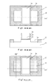
Currently, a method for forming a semiconductor device comprises the following steps. Firstly, as illustrated in FIGS. 1 and 2, an active region 20 and an isolation region 12 surrounding the active region 20 are formed on a semiconductor substrate 10. Next, as illustrated in FIGS. 3 and 4, a gate stack structure is formed on the active region 20 and extends to the isolation region 12 (the gate stack structure comprises a gate dielectric layer 22, a gate 24 formed on the gate dielectric layer 22, and sidewalls 26 surrounding the gate dielectric layer 22 and the gate 24. In practice, a cap layer is further formed on the gate for preventing the gate from being damaged during the operation. The cap layer is usually made of silicon nitride. The cap layer is not indicated in the text and drawings of this specification for the convenience of description). Next, as illustrated in FIGS. 5 and 6, the gate stack structure and the isolation region 12 are used as a mask, and the semiconductor substrate 10 of a partial thickness in the active region 20 is removed to form a groove 30. Finally, a semiconductor material is produced in the groove 30 for filling into the groove 30 so as to form a source/drain (S/D) region.
However, as illustrated in FIGS. 7 to 9, it is found in practice that a slot 34 is defined at an interface between the S/D region 32 and the isolation region 12. Consequently, as illustrated in FIGS. 10 to 12, when a contact region 36 (e.g., metal silicide layer) is formed subsequently on the S/D region 32, the contact region 36 may likely reach a junction region via the slot 34, thereby causing a leakage current.
SUMMARY OF THE INVENTION
In order to solve the above problem, the present invention provides an isolation region, a semiconductor device and methods for forming the same, which are beneficial to reduce the leakage current.
The present invention provides an isolation region, comprising: a first groove and an insulation layer filling the first groove, wherein the first groove is embedded into a semiconductor substrate and comprises a first sidewall, a bottom surface and a second sidewall that extends from the bottom surface and joins to the first sidewall, and an angle between the first sidewall and a normal line of the semiconductor substrate is larger than a standard value.
Optionally, the angle between the first sidewall and the normal line of the semiconductor substrate is in the range from about 5° to about 20° (5°˜20°.
Optionally, in any cross-sectional plane perpendicular to the semiconductor substrate, the second sidewall is joined to the first sidewall at a first joint and a second joint, and an angle between the second sidewall and the normal line of the semiconductor substrate increases from the first joint to the second joint.
A semiconductor device comprising the above isolation region, the semiconductor device further comprises an S/D region, and the S/D region comprises a second groove and a semiconductor layer filling the second groove, wherein there is material of the semiconductor substrate interposed between the second groove and the first and second sidewalls.
Optionally, when the material of the semiconductor substrate is Si, for a PMOS device, the semiconductor layer is Si1-xGex, and for an NMOS device, the semiconductor layer is Si:C.
A method for forming an isolation region, comprising: forming a first trench on a semiconductor substrate, wherein an angle between a sidewall of the first trench and a normal line of the semiconductor substrate is larger than a standard value; forming a mask on the sidewall to form a second trench on the semiconductor substrate by using the mask; and forming an insulation layer to fill the first and second trenches.
Optionally, the angle between the sidewall and the normal line of the semiconductor substrate is about 5°˜about 20°.
Optionally, before the insulation layer is formed, the method further comprises performing an etching operation on the second trench to expand the second trench.
A method for forming a semiconductor device, comprising: forming the isolation region using the above method, so as to isolate active regions; forming on the semiconductor substrate a gate stack structure that resides on the active region and extends to the isolation region; using the gate stack structure and the isolation region as a mask to form a third trench in the active region, wherein there is material of the semiconductor substrate interposed between the third trench and the isolation region; and filling a semiconductor layer into the third trench to form an S/D region.
Optionally, when the material of the semiconductor substrate is Si, for a PMOS device, the semiconductor layer is Si1-XGeX, and for an NMOS device, the semiconductor layer is Si:C.
As compared with the prior art, the technical solution of the present invention has the following advantages:
On the premise that opening areas of the isolation region are the same, the cross-sectional area of the embedded isolation region is made to be smaller than the opening area by increasing the angle between the first sidewall (i.e., the sidewall of the first trench) and the nominal line of the semiconductor substrate. In the subsequent steps, the S/D region is formed by using the opening of the isolation region as the mask. In addition, when the groove bearing the material of the S/D region is formed, an anisotropic etching process is adopted, so that the active region connected to the isolation region is removed at the opening of the isolation region. In any cross-sectional plane parallel to the top surface of the semiconductor substrate, the active region joined to the isolation region will no longer be removed since the cross-section area of the isolation region is reduced, i.e., the embedded isolation region is still joined to the material of the active region (i.e., the material of the semiconductor substrate). In other words, the material of the semiconductor substrate is retained between the groove and the isolation region. That is to say, each wall of the groove is made of the material of the semiconductor substrate (wherein, the sidewall of the groove close to the isolation region is made of the material of the semiconductor substrate, instead of the material of the isolation region, due to the material of the semiconductor substrate remaining between the groove and the isolation region). Then the material of the semiconductor substrate is used as seed crystal to grow the material of the S/D region in the groove (when the material of the semiconductor substrate is Si, for a PMOS device, the semiconductor layer is Si1-XGeX, and for an NMOS device, the semiconductor layer is Si:C). This is beneficial to reduce the possibility of defining a slot at an interface between the formed S/D region and the isolation region. Furthermore, due to the reduction of the possibility of defining the slot, a stress loss will also be reduced when the material of the S/D region is formed in the groove.
In any cross-sectional plane perpendicular to the semiconductor substrate, from the first joint to the second joint, the angle between the second sidewall and the normal line of the semiconductor substrate increases. This is beneficial to expand the cross-sectional area of a region defined by the second sidewall. Then, the above region is filled with the insulation layer to form the isolation region, and this is beneficial to enhance the isolation effect; or before the insulation layer is formed, an etching operation is performed on the second groove to expand the second groove, which may increase the cross-section area of the second groove. Then, the second groove is filled with the insulation layer, and this is beneficial to enhance the isolation effect.
BRIEF DESCRIPTION OF THE DRAWINGS
The following sectional views are all obtained by cutting the formed structures along lines AA′ and BB′ shown in corresponding top views.
FIGS. 1˜2 illustrate structural diagrams after an active region is formed according to the prior art.
FIGS. 3˜4 illustrate structural diagrams after a gate stack structure is formed according to the prior art.
FIGS. 5˜6 illustrate structural diagrams after a groove is formed according to the prior art.
FIGS. 7˜9 illustrate structural diagrams after an S/D region is formed according to the prior art.
FIGS. 10˜12 illustrate structural diagrams after a contact region is formed according to the prior art.
FIG. 13 illustrates a structural diagram of a first embodiment of an isolation region according to the present invention.
FIG. 14 illustrates a structural diagram of a second embodiment of an isolation region according to the present invention.
FIG. 15 illustrates a structural diagram of an embodiment of a semiconductor device according to the present invention.
FIG. 16 illustrates a structural diagram after a first trench is formed in a first embodiment of a method for forming an isolation region according to the present invention.
FIG. 17 illustrates a structural diagram after a second trench is formed in the first embodiment of a method for forming an isolation region according to the present invention.
FIG. 18 illustrates a structural diagram after a second trench is formed in a second embodiment of a method for forming an isolation region according to the present invention.
FIG. 19 illustrates a structural diagram after an insulation layer is formed in the first embodiment of a method for forming an isolation region according to the present invention.
FIG. 20 illustrates a structural diagram after an isolation region is formed in an embodiment of a method for forming a semiconductor device according to the present invention.
FIG. 21 illustrates a structural diagram after a gate stack structure is formed in an embodiment of a method for forming a semiconductor device according to the present invention.
FIG. 22 illustrates a structural diagram after a third trench is formed in an embodiment of a method for forming a semiconductor device according to the present invention.
FIG. 23 illustrates a structural diagram after a semiconductor layer is formed in an embodiment of a method for forming a semiconductor device according to the present invention.
DETAILED DESCRIPTION OF THE EMBODIMENTS
The following text provides many different embodiments or examples to implement the technical solution of the present invention. Although descriptions of the components and arrangements of specific examples are given as follows, they are just exemplary, and do not intend to limit the present invention.
In addition, reference numbers and/or letters can be repeatedly used in different embodiments of the present invention for the purposes of simplification and clearness, without indicating the relationships between the discussed embodiments and/or arrangements.
The present invention provides examples of various specific processes and/or materials. But it is apparent that substitutive applications of other processes and/or materials conceivable by a person skilled in the art do not deviate from the scope of the present invention. To be emphasized, the interfaces of various regions described in this specification include necessary extensions made according to the requirements of the processes or procedures.
As illustrated in FIG. 13, the present invention provides an isolation region comprising a first groove 120 and an insulation layer 140 filling the first groove 120. The first groove 120 is embedded into a semiconductor substrate 100 and comprises a first sidewall 122, a bottom surface 126 and a second sidewall 124 that extends from the bottom surface 126 and joins to the first sidewall 122. In which, an angle between the first sidewall 122 and a normal line of the semiconductor substrate 100 (as indicated by a dashed line in the drawing) is larger than a standard value.
Herein the standard value means that when the groove 120 is to be etched in practice, if an angle between the sidewall of the groove 120 and the normal line of the semiconductor substrate 100 is designed to be α, while an angle actually obtained to meet the design requirement is α+ α due to the demand of the process or procedure (e.g., there exists a process error or the subsequent filling effect needs to be improved), then α is a standard value.
In the present embodiment, the semiconductor substrate 100 is a substrate of silicon, and in other embodiments, the semiconductor substrate 100 may also be made of other compound semiconductor, such as silicon carbide (SiC), gallium arsenide (GaAs), indium arsenide (InAs) or indium phosphide (InP). In addition, the semiconductor substrate 100 preferably includes an epitaxial layer. The semiconductor substrate 100 may also include a silicon on insulator (SOI) structure. The insulation layer 140 may be made of silicon nitride, silicon oxynitride or non-doped silicon oxide.
In the present embodiment, the angle between the first sidewall 122 and the normal line of the semiconductor substrate 100 may be about 5°˜about 20°, such as 8°, 10° or 15°. On the premise that the opening areas of the isolation region are the same, the cross-sectional area of the embedded isolation region is made to be smaller than the opening area. Then, in the following step, the material of the semiconductor substrate 100 may be residual between the groove bearing the material of an S/D region and the isolation region, i.e., each wall of the groove is made of the material of the semiconductor substrate 100. This is beneficial to reduce the possibility of defining a slot at an interface between the formed S/D region and the isolation region.
Particularly, in a second embodiment of the isolation region, the present invention further provides an isolation region. In which, in any cross-sectional plane perpendicular to the semiconductor substrate 100 (for example, the cross-section as illustrated in FIG. 14), the second sidewall 124 is joined to the first sidewall 122 at a first joint 1224 and a second joint 1242. From the first joint 1224 to the second joint 1242, an angle between the second sidewall 124 and the normal line of the semiconductor substrate 100 increases. This is beneficial to expand a cross-sectional area of a region defined by the second sidewall 124. Then, the above region is filled with the insulation layer 140 to form the isolation region, and this is beneficial to enhance the isolation effect. To be noted, in any cross-sectional plane perpendicular to the semiconductor substrate 100, the second sidewall 124 may have an arc shape, a fold line shape (not shown), etc.
As illustrated in FIG. 15, the present invention provides a semiconductor device comprising the above isolation region (taking the second embodiment for example). The semiconductor device further comprises a gate stack structure (the gate stack structure comprises a gate dielectric layer 102, a gate 104 formed on the gate dielectric layer 102, and sidewalls 106 surrounding the gate dielectric layer 102 and the gate 104, which are beneficial to reduce a parasitic capacitance; and in other embodiments, the sidewalls 106 may be located on the gate dielectric layer 102 and surround the gate 104) and an S/D region (taking an embedded source/drain region for example). In which, the S/D region comprises a second groove 144 and a semiconductor layer 146 filling the second groove 144. The material of the semiconductor substrate 100 is interposed between the second groove 144 and the first and second sidewalls 122, 124 (indicated by a dashed frame in the drawing). That is to say, when the second groove 144 bearing the material of the S/D region is formed, each wall of the second groove 144 is made of the material of the semiconductor substrate 100, and then the material of the semiconductor substrate 100 is used as seed crystal. This is beneficial for a uniform growth of the semiconductor layer 146 for forming the S/D region along each direction in the second groove 144, so as to reduce the possibility of defining a slot at an interface between the formed S/D region and the isolation region 142.
When the semiconductor substrate 100 is Si, for the PMOS device, the semiconductor layer may be Si1-XGeX (the value range of X may be about 0.1˜about 0.7, which can be flexibly adjusted according to a process requirement, such as 0.2, 0.3, 0.4, 0.5 or 0.6, and the value of X in this specification is the same as that indicated herein unless otherwise specified); for the NMOS device, the semiconductor layer may be Si:C (the atomic percentage of C may be about 0.2%˜about 2%, such as 0.5%, 1% or 1.5%, the content of C may be flexibly adjusted according to a process requirement, and the atomic percentage of C in this specification is the same as that indicated herein unless otherwise specified). To be noted, the semiconductor layer may be made of a semiconductor material doped with ions, e.g., Si1-XGeX or Si:C of N type or P type. The ion doping operation may be performed directly during the production of the semiconductor material (e.g., adding a reactant containing the doped ion components into reactants for producing the semiconductor material), or performed through an ion implantation process after the semiconductor material is produced. Any conventional ion implantation process may be adopted to perform the ion doping operation, which herein is not described in detail.
Forming the S/D region with the above material is beneficial to adjust the stress in the channel region of the semiconductor device by using the stress provided by the S/D region, so as to improve the mobility of carriers in the channel region. Forming the S/D region using the method provided by the present invention is beneficial to reduce the stress loss of the S/D region.
The invention further provides a method for forming an isolation region, comprising:
Firstly, as illustrated in FIG. 16, a first trench 220 is formed on a semiconductor substrate 200. An angle between a sidewall 222 of the first trench 220 and a normal line of the semiconductor substrate 200 (as indicated by a dashed line in the drawing) is larger than a standard value.
The semiconductor substrate 200 is a substrate of silicon, and in other embodiments, the semiconductor substrate 200 may also be made of other compound semiconductor such as silicon carbide (SiC), gallium arsenide (GaAs), indium arsenide (InAs) or indium phosphide (InP). In addition, the semiconductor substrate 200 preferably includes an epitaxial layer. The semiconductor substrate 200 may also include a silicon on insulator (SOI) structure.
The step of forming the first trench 220 comprises: forming silicon oxide (using a thermal oxidation process or a deposition process) and silicon nitride in sequence on the semiconductor substrate 200 (using a deposition process); next, forming a patterned photoresist layer on the silicon nitride; next, using the patterned photoresist layer as a mask to pattern the silicon nitride and the silicon oxide, so as to form a hard mask 224 (i.e., in order to make the structure clear, the illustrated hard mask 224 contains the silicon oxide and the silicon nitride formed thereon); next, removing the patterned photoresist layer; and finally, etching the semiconductor substrate 200 of a partial thickness by using the hard mask 224.
In the prior art, the reasons why a slot is defined between the S/D region and the isolation region are as follows. The S/D region is formed by filling a semiconductor material into a trench, and the semiconductor material is produced through an epitaxial process. The gate stack structure and the isolation region are used as the mask when the trench is formed. That is, the sidewalls of the isolation region will be exposed after the trench is formed. In other words, walls of the trench include both the material of the semiconductor substrate and the sidewall of the isolation region. When the semiconductor material is produced through the epitaxial process, the material of the semiconductor substrate is used as the seed crystal, i.e., the sidewall of the isolation region used as the wall of the trench cannot provide the seed crystal. In addition, it is found that the semiconductor material has different growth rates along different crystal orientations. Specifically, as compared with orientations (100) and (110), the semiconductor material has a slower growth rate along the orientation (111). In practice, an orientation perpendicular to the semiconductor substrate 100 generally is the orientation (100), and an orientation parallel to the semiconductor substrate 100 is the orientation (110). Then the orientation (111) obliquely crosses the orientations (100) and (110). That is, since the semiconductor material has a slower growth rate along the orientation (111), the semiconductor material will form an oblique side surface (along the orientation (111)), and a slot will be defined between the oblique side surface and the sidewalls of the isolation region 120.
It is considered that it is beneficial to reduce or even eliminate the slot between the S/D region and the isolation region so as to reduce the leakage current when the material of the semiconductor substrate is retained or formed on the sidewalls of the isolation region. In other words, the proportion of the material of the semiconductor substrate in the walls of the trench is increased. That is, by supplying the material of the semiconductor substrate having different crystal orientations as the seed crystal, the above slot is filled by the semiconductor material formed by the epitaxial growth of the supplied seed crystal.
In the present embodiment, the first trench 220 may be formed through an etching process. The angle between the sidewall 222 and the normal line of the semiconductor substrate 200 may be about 5°˜about 20°, such as 8°, 10° or 15°.
Subsequently, as illustrated in FIG. 17, a mask 240 is formed on the sidewall 222, and a second trench 260 is formed on the semiconductor substrate 200 by using the mask 240.
The mask 240 may be any semiconductor material rather than the material of the semiconductor substrate 200, such as silicon nitride, silicon oxynitride or non-doped silicon oxide. The material of the mask 240 may be the same as the material of the insulation layer for filling the trench subsequently so as to form the isolation region, e.g., when the material of the insulation layer for filling the trench subsequently so as to form the isolation region is the non-doped silicon oxide, the material of the mask may also be the non-doped silicon oxide. This is beneficial for compatibility of the technical solution of the present invention with the conventional process. The mask 240 may be formed by using a selective deposition process. The second trench 260 may be formed by using an etching process.
Other embodiments may further comprise: performing an etching operation on the second trench 260 to expand the second trench 260. An isotropic or anisotropic etching process may be adopted to perform the operation for expansion of the second trench 260. Taking the operation for expansion being performed by using the isotropic etching process for example, as illustrated in FIG. 18, herein in any cross-sectional plane (e.g., the cross-section as illustrated in the drawing) perpendicular to the top surface of the semiconductor substrate 200, the sidewall 262 of the second trench 260 may have an arc shape. When the operation for expansion is performed by using the anisotropic etching process, the sidewall of the second trench 260 may have a fold line shape (not shown).
The cross-sectional area of the second trench 260 may be increased by performing an etching operation on the second trench 260 to expand the second trench 260. Consequently, the second trench 260 is filled by the insulation layer and this is beneficial to enhance the insulation effect.
Next, as illustrated in FIG. 19, an insulation layer 280 is formed to fill the first trench 220 and the second trench 260.
The insulation layer 280 may be silicon nitride, silicon oxynitride or non-doped silicon oxide. Before the insulation layer 280 is formed, the mask 240 may be removed or not removed (in this embodiment, an example is taken to remove the mask, or wherein the material of the mask is the same as that of the insulation layer). The hard mask 224 will also be removed before subsequent steps.
The present invention further provides a method for forming a semiconductor device, and the method comprises the following steps. Firstly, as illustrated in FIG. 20, an isolation region 142 is formed using the above method (e.g., see the second embodiment of the isolation region) to isolate active regions 148. Next, as illustrated in FIG. 21, a gate stack structure (the same as that described in the embodiment of the aforementioned semiconductor device, and herein is not repeated) is formed on the semiconductor substrate 100. The gate stack structure passes through the active region 148 and extends to the isolation region 142. Next, as illustrated in FIG. 22, the gate stack structure and the isolation region are used as the mask to form a third trench 150 in the active region. Finally, as illustrated in FIG. 23, a semiconductor layer 152 is filled into the third trench 150 to form an S/D region. The third trench 150 may be formed by using an anisotropic etching process. The material of the semiconductor layer 152 is the same as that described in the embodiment of the aforementioned semiconductor device, and herein is not repeated.
On the premise that the opening areas of the isolation region are the same, the cross-sectional area of the embedded isolation region is made to be smaller than the opening area by increasing the angle between the sidewall of the first trench and the nominal line of the semiconductor substrate. In the subsequent steps, the S/D region is formed by using the opening of the isolation region as the mask. In addition, when the third trench bearing the material of the S/D region is formed, the anisotropic etching process is adopted, so that the active region connected to the isolation region is removed at the opening of the isolation region. On any cross-section parallel to the semiconductor substrate, the active region joined to the isolation region will no longer be removed since the cross-section area of the isolation region is reduced, i.e., the embedded isolation region is still joined to the material of the active region (i.e., the material of the semiconductor substrate). In other words, the material of the semiconductor substrate is residual between the third trench and the isolation region. That is to say, each wall of the third trench is made of the material of the semiconductor substrate. Then the material of the semiconductor substrate is used as seed crystal. This is beneficial for a uniform growth of the semiconductor material for forming the S/D region along each direction in the trench, and thus beneficial to reduce the possibility of defining a slot at an interface between the formed S/D region and the isolation region.
Furthermore, the scope of the present invention is not limited to the processes, structures, manufacturing, compositions, means, methods and steps of the specific embodiments as described in the specification. According to the disclosure of present invention, a person skilled in the art will easily appreciate that, when the processes, structures, manufacturing, compositions, means, methods and steps currently existing or to be developed in future are adopted to perform functions substantially the same as corresponding embodiments described in the present invention, or achieve substantially the same effects, a person skilled in the art can make applications of them under the teaching of the present invention, without deviating from the scope of the present invention.

Claims (3)

What is claimed is:
1. A semiconductor structure, comprising:
a first groove and an insulation layer filling the first groove, wherein the first groove is embedded into a semiconductor substrate and includes a top portion and a bottom portion, wherein the top portion is surrounded by a first sidewall, wherein the bottom portion is surrounded by a second sidewall and includes a bottom surface, wherein the first sidewall, the second sidewall, and the bottom surface are arranged along a thicknesses direction of the semiconductor substrate; and wherein in any cross-sectional plane perpendicular to the semiconductor substrate, the second sidewall has a cross-section view with an arc profile or a fold-line profile, wherein an angle between the first sidewall and a normal line of the semiconductor substrate is larger than an angle between the second sidewall and the normal line of the semiconductor substrate; and
a source/drain (S/D) region, wherein the S/D region comprises a second groove and a semiconductor layer filling the second groove,
wherein the material of the semiconductor substrate is interposed between the first groove and the second groove in both a length direction and a width direction of a gate.
2. The semiconductor structure according to claim 1, wherein the angle between the first sidewall and the normal line of the semiconductor substrate is in a range from about 5° to about 20°.
3. The semiconductor according to claim 1, wherein when a material of the semiconductor substrate is Si, for a PMOS device, the semiconductor layer is Si1-XGeX; and for an NMOS device, the semiconductor layer is Si:C.
US13/119,129 2010-07-01 2011-02-18 Isolation region, semiconductor device and methods for forming the same Active 2031-09-14 US9082717B2 (en)

Applications Claiming Priority (4)

Application Number Priority Date Filing Date Title
CN201010223894.2 2010-07-01
CN201010223894 2010-07-01
CN2010102238942A CN102315152A (en) 2010-07-01 2010-07-01 Isolation area, semiconductor device and forming method thereof
PCT/CN2011/071093 WO2012000316A1 (en) 2010-07-01 2011-02-18 Isolation region, semiconductor device and manufacturing method thereof

Publications (2)

Publication Number Publication Date
US20120001198A1 US20120001198A1 (en) 2012-01-05
US9082717B2 true US9082717B2 (en) 2015-07-14

Family

ID=45401367

Family Applications (1)

Application Number Title Priority Date Filing Date
US13/119,129 Active 2031-09-14 US9082717B2 (en) 2010-07-01 2011-02-18 Isolation region, semiconductor device and methods for forming the same

Country Status (4)

Country Link
US (1) US9082717B2 (en)
CN (2) CN102315152A (en)
GB (1) GB2486978B (en)
WO (1) WO2012000316A1 (en)

Families Citing this family (6)

* Cited by examiner, † Cited by third party
Publication number Priority date Publication date Assignee Title
CN102237396B (en) 2010-04-27 2014-04-09 中国科学院微电子研究所 Semiconductor device and manufacturing method thereof
US8623713B2 (en) * 2011-09-15 2014-01-07 International Business Machines Corporation Trench isolation structure
US8629008B2 (en) * 2012-01-11 2014-01-14 International Business Machines Corporation Electrical isolation structures for ultra-thin semiconductor-on-insulator devices
CN104392956A (en) * 2014-11-26 2015-03-04 上海华力微电子有限公司 Semiconductor device manufacturing method
CN104409412A (en) * 2014-11-26 2015-03-11 上海华力微电子有限公司 STI (shallow trench isolation) edge epitaxial layer performance improving method and corresponding semiconductor structure
CN113345805A (en) * 2021-06-04 2021-09-03 长江存储科技有限责任公司 Manufacturing method of semiconductor device and semiconductor device

Citations (6)

* Cited by examiner, † Cited by third party
Publication number Priority date Publication date Assignee Title
CN1953141A (en) 2005-10-17 2007-04-25 恩益禧电子股份有限公司 Fabrication method of semiconductor device
JP2008192821A (en) 2007-02-05 2008-08-21 Matsushita Electric Ind Co Ltd Semiconductor device and manufacturing method therefor
CN101540315A (en) 2008-03-17 2009-09-23 联华电子股份有限公司 Semiconductor device and forming method thereof
US20100203692A1 (en) * 2007-02-12 2010-08-12 Samsung Electronics Co., Ltd. Methods of fabricating integrated circuit devices including strained channel regions and related devices
US20110278646A1 (en) * 2008-11-03 2011-11-17 Taiwan Semiconductor Manufacturing Company, Ltd. Balance Step-Height Selective Bi-Channel Structure on HKMG Devices
US20110303982A1 (en) * 2008-09-10 2011-12-15 Taiwan Semiconductor Manufacturing Company, Ltd. Resistive Device for High-K Metal Gate Technology and Method of Making the Same

Family Cites Families (4)

* Cited by examiner, † Cited by third party
Publication number Priority date Publication date Assignee Title
JPH1174339A (en) * 1997-08-28 1999-03-16 Mitsubishi Electric Corp Semiconductor device and manufacture thereof
US20070224775A1 (en) * 2006-03-27 2007-09-27 Nick Lindert Trench isolation structure having an expanded portion thereof
US20080242032A1 (en) * 2007-03-29 2008-10-02 Texas Instruments Incorporated Carbon-Doped Epitaxial SiGe
US7772095B2 (en) * 2008-05-28 2010-08-10 International Business Machines Corporation Integrated circuit having localized embedded SiGe and method of manufacturing

Patent Citations (6)

* Cited by examiner, † Cited by third party
Publication number Priority date Publication date Assignee Title
CN1953141A (en) 2005-10-17 2007-04-25 恩益禧电子股份有限公司 Fabrication method of semiconductor device
JP2008192821A (en) 2007-02-05 2008-08-21 Matsushita Electric Ind Co Ltd Semiconductor device and manufacturing method therefor
US20100203692A1 (en) * 2007-02-12 2010-08-12 Samsung Electronics Co., Ltd. Methods of fabricating integrated circuit devices including strained channel regions and related devices
CN101540315A (en) 2008-03-17 2009-09-23 联华电子股份有限公司 Semiconductor device and forming method thereof
US20110303982A1 (en) * 2008-09-10 2011-12-15 Taiwan Semiconductor Manufacturing Company, Ltd. Resistive Device for High-K Metal Gate Technology and Method of Making the Same
US20110278646A1 (en) * 2008-11-03 2011-11-17 Taiwan Semiconductor Manufacturing Company, Ltd. Balance Step-Height Selective Bi-Channel Structure on HKMG Devices

Non-Patent Citations (3)

* Cited by examiner, † Cited by third party
Title
Examination Report from Great Britain Intellectual Property Office dated Aug. 13, 2014.
Internation Search Report to PCT/CN2011/071093.
Office Action to Great Britain Equivalent GB 1122114.0 dated Jan. 31, 2014.

Also Published As

Publication number Publication date
CN202585379U (en) 2012-12-05
GB2486978B (en) 2015-02-11
WO2012000316A1 (en) 2012-01-05
GB2486978A (en) 2012-07-04
GB201122114D0 (en) 2012-02-01
US20120001198A1 (en) 2012-01-05
CN102315152A (en) 2012-01-11

Similar Documents

Publication Publication Date Title
KR101756536B1 (en) Semiconductor structures and methods of forming the same
US20200051871A1 (en) Method of forming source/drain regions of transistors
CN102194755B (en) Fin field effect transistor and method of making the same
KR100657395B1 (en) Semiconductor device and manufacturing method of the same
KR101115091B1 (en) Semiconductor structure with different lattice constant materials and method for forming the same
US9006057B2 (en) Method of manufacturing semiconductor device
US9082717B2 (en) Isolation region, semiconductor device and methods for forming the same
US20120043624A1 (en) Ultra-thin body transistor and method for manufcturing the same
US10236216B2 (en) Method for manufacturing a semiconductor device having a fin located on a substrate
KR20190003295A (en) Semiconductor device and method
US20100327329A1 (en) Semiconductor device and method of fabricating the same
US20120187501A1 (en) Semiconductor structure and method for manufacturing the same
KR20060059088A (en) Method of fabricating transistor including buried insulating layer and transistor fabricated thereby
US8692335B2 (en) Source/drain region, contact hole and method for forming the same
US20130313655A1 (en) Semiconductor device and a method for manufacturing the same
US8927352B2 (en) Channel epitaxial regrowth flow (CRF)
US10325813B2 (en) Fin cut process and fin structure
US20060121687A1 (en) Semiconductor device having a multi-bridge-channel and method for fabricating the same
US8524565B2 (en) Semiconductor device and method for forming the same
US9099309B2 (en) Method providing an epitaxial growth having a reduction in defects and resulting structure
US8264017B2 (en) Junction field effect transistor having a double gate structure
US8703567B2 (en) Method for manufacturing a semiconductor device
CN105719971B (en) The forming method of semiconductor devices
US10600890B2 (en) Contact to metal gate isolation structure
US9349808B2 (en) Double aspect ratio trapping

Legal Events

Date Code Title Description
AS Assignment

Owner name: INSTITUTE OF MICROELECTRONICS, CHINESE ACADEMY OF

Free format text: ASSIGNMENT OF ASSIGNORS INTEREST;ASSIGNORS:YIN, HAIZHOU;ZHU, HUILONG;LUO, ZHIJIONG;SIGNING DATES FROM 20110309 TO 20110310;REEL/FRAME:025959/0129

STCF Information on status: patent grant

Free format text: PATENTED CASE

MAFP Maintenance fee payment

Free format text: PAYMENT OF MAINTENANCE FEE, 4TH YR, SMALL ENTITY (ORIGINAL EVENT CODE: M2551); ENTITY STATUS OF PATENT OWNER: SMALL ENTITY

Year of fee payment: 4

MAFP Maintenance fee payment

Free format text: PAYMENT OF MAINTENANCE FEE, 8TH YR, SMALL ENTITY (ORIGINAL EVENT CODE: M2552); ENTITY STATUS OF PATENT OWNER: SMALL ENTITY

Year of fee payment: 8