US9054068B2 - Etchstop layers and capacitors - Google Patents
Etchstop layers and capacitors Download PDFInfo
- Publication number
- US9054068B2 US9054068B2 US13/977,647 US201113977647A US9054068B2 US 9054068 B2 US9054068 B2 US 9054068B2 US 201113977647 A US201113977647 A US 201113977647A US 9054068 B2 US9054068 B2 US 9054068B2
- Authority
- US
- United States
- Prior art keywords
- layer
- etchstop
- dielectric
- comprised
- conducting material
- Prior art date
- Legal status (The legal status is an assumption and is not a legal conclusion. Google has not performed a legal analysis and makes no representation as to the accuracy of the status listed.)
- Active, expires
Links
Images


Classifications
-
- H—ELECTRICITY
- H01—ELECTRIC ELEMENTS
- H01L—SEMICONDUCTOR DEVICES NOT COVERED BY CLASS H10
- H01L28/00—Passive two-terminal components without a potential-jump or surface barrier for integrated circuits; Details thereof; Multistep manufacturing processes therefor
- H01L28/40—Capacitors
-
- H—ELECTRICITY
- H01—ELECTRIC ELEMENTS
- H01L—SEMICONDUCTOR DEVICES NOT COVERED BY CLASS H10
- H01L28/00—Passive two-terminal components without a potential-jump or surface barrier for integrated circuits; Details thereof; Multistep manufacturing processes therefor
- H01L28/40—Capacitors
- H01L28/60—Electrodes
-
- G—PHYSICS
- G06—COMPUTING; CALCULATING OR COUNTING
- G06F—ELECTRIC DIGITAL DATA PROCESSING
- G06F1/00—Details not covered by groups G06F3/00 - G06F13/00 and G06F21/00
- G06F1/16—Constructional details or arrangements
- G06F1/18—Packaging or power distribution
- G06F1/183—Internal mounting support structures, e.g. for printed circuit boards, internal connecting means
- G06F1/184—Mounting of motherboards
-
- H—ELECTRICITY
- H01—ELECTRIC ELEMENTS
- H01L—SEMICONDUCTOR DEVICES NOT COVERED BY CLASS H10
- H01L21/00—Processes or apparatus adapted for the manufacture or treatment of semiconductor or solid state devices or of parts thereof
- H01L21/02—Manufacture or treatment of semiconductor devices or of parts thereof
- H01L21/02104—Forming layers
- H01L21/02107—Forming insulating materials on a substrate
- H01L21/02109—Forming insulating materials on a substrate characterised by the type of layer, e.g. type of material, porous/non-porous, pre-cursors, mixtures or laminates
- H01L21/02112—Forming insulating materials on a substrate characterised by the type of layer, e.g. type of material, porous/non-porous, pre-cursors, mixtures or laminates characterised by the material of the layer
- H01L21/02172—Forming insulating materials on a substrate characterised by the type of layer, e.g. type of material, porous/non-porous, pre-cursors, mixtures or laminates characterised by the material of the layer the material containing at least one metal element, e.g. metal oxides, metal nitrides, metal oxynitrides or metal carbides
- H01L21/02175—Forming insulating materials on a substrate characterised by the type of layer, e.g. type of material, porous/non-porous, pre-cursors, mixtures or laminates characterised by the material of the layer the material containing at least one metal element, e.g. metal oxides, metal nitrides, metal oxynitrides or metal carbides characterised by the metal
- H01L21/02178—Forming insulating materials on a substrate characterised by the type of layer, e.g. type of material, porous/non-porous, pre-cursors, mixtures or laminates characterised by the material of the layer the material containing at least one metal element, e.g. metal oxides, metal nitrides, metal oxynitrides or metal carbides characterised by the metal the material containing aluminium, e.g. Al2O3
-
- H—ELECTRICITY
- H01—ELECTRIC ELEMENTS
- H01L—SEMICONDUCTOR DEVICES NOT COVERED BY CLASS H10
- H01L21/00—Processes or apparatus adapted for the manufacture or treatment of semiconductor or solid state devices or of parts thereof
- H01L21/02—Manufacture or treatment of semiconductor devices or of parts thereof
- H01L21/02104—Forming layers
- H01L21/02107—Forming insulating materials on a substrate
- H01L21/02109—Forming insulating materials on a substrate characterised by the type of layer, e.g. type of material, porous/non-porous, pre-cursors, mixtures or laminates
- H01L21/02112—Forming insulating materials on a substrate characterised by the type of layer, e.g. type of material, porous/non-porous, pre-cursors, mixtures or laminates characterised by the material of the layer
- H01L21/02172—Forming insulating materials on a substrate characterised by the type of layer, e.g. type of material, porous/non-porous, pre-cursors, mixtures or laminates characterised by the material of the layer the material containing at least one metal element, e.g. metal oxides, metal nitrides, metal oxynitrides or metal carbides
- H01L21/02175—Forming insulating materials on a substrate characterised by the type of layer, e.g. type of material, porous/non-porous, pre-cursors, mixtures or laminates characterised by the material of the layer the material containing at least one metal element, e.g. metal oxides, metal nitrides, metal oxynitrides or metal carbides characterised by the metal
- H01L21/02181—Forming insulating materials on a substrate characterised by the type of layer, e.g. type of material, porous/non-porous, pre-cursors, mixtures or laminates characterised by the material of the layer the material containing at least one metal element, e.g. metal oxides, metal nitrides, metal oxynitrides or metal carbides characterised by the metal the material containing hafnium, e.g. HfO2
-
- H—ELECTRICITY
- H01—ELECTRIC ELEMENTS
- H01L—SEMICONDUCTOR DEVICES NOT COVERED BY CLASS H10
- H01L21/00—Processes or apparatus adapted for the manufacture or treatment of semiconductor or solid state devices or of parts thereof
- H01L21/02—Manufacture or treatment of semiconductor devices or of parts thereof
- H01L21/02104—Forming layers
- H01L21/02107—Forming insulating materials on a substrate
- H01L21/02109—Forming insulating materials on a substrate characterised by the type of layer, e.g. type of material, porous/non-porous, pre-cursors, mixtures or laminates
- H01L21/02112—Forming insulating materials on a substrate characterised by the type of layer, e.g. type of material, porous/non-porous, pre-cursors, mixtures or laminates characterised by the material of the layer
- H01L21/02172—Forming insulating materials on a substrate characterised by the type of layer, e.g. type of material, porous/non-porous, pre-cursors, mixtures or laminates characterised by the material of the layer the material containing at least one metal element, e.g. metal oxides, metal nitrides, metal oxynitrides or metal carbides
- H01L21/02175—Forming insulating materials on a substrate characterised by the type of layer, e.g. type of material, porous/non-porous, pre-cursors, mixtures or laminates characterised by the material of the layer the material containing at least one metal element, e.g. metal oxides, metal nitrides, metal oxynitrides or metal carbides characterised by the metal
- H01L21/02186—Forming insulating materials on a substrate characterised by the type of layer, e.g. type of material, porous/non-porous, pre-cursors, mixtures or laminates characterised by the material of the layer the material containing at least one metal element, e.g. metal oxides, metal nitrides, metal oxynitrides or metal carbides characterised by the metal the material containing titanium, e.g. TiO2
-
- H—ELECTRICITY
- H01—ELECTRIC ELEMENTS
- H01L—SEMICONDUCTOR DEVICES NOT COVERED BY CLASS H10
- H01L21/00—Processes or apparatus adapted for the manufacture or treatment of semiconductor or solid state devices or of parts thereof
- H01L21/02—Manufacture or treatment of semiconductor devices or of parts thereof
- H01L21/04—Manufacture or treatment of semiconductor devices or of parts thereof the devices having at least one potential-jump barrier or surface barrier, e.g. PN junction, depletion layer or carrier concentration layer
- H01L21/18—Manufacture or treatment of semiconductor devices or of parts thereof the devices having at least one potential-jump barrier or surface barrier, e.g. PN junction, depletion layer or carrier concentration layer the devices having semiconductor bodies comprising elements of Group IV of the Periodic System or AIIIBV compounds with or without impurities, e.g. doping materials
- H01L21/30—Treatment of semiconductor bodies using processes or apparatus not provided for in groups H01L21/20 - H01L21/26
- H01L21/31—Treatment of semiconductor bodies using processes or apparatus not provided for in groups H01L21/20 - H01L21/26 to form insulating layers thereon, e.g. for masking or by using photolithographic techniques; After treatment of these layers; Selection of materials for these layers
- H01L21/3105—After-treatment
- H01L21/311—Etching the insulating layers by chemical or physical means
- H01L21/31144—Etching the insulating layers by chemical or physical means using masks
-
- H—ELECTRICITY
- H01—ELECTRIC ELEMENTS
- H01L—SEMICONDUCTOR DEVICES NOT COVERED BY CLASS H10
- H01L21/00—Processes or apparatus adapted for the manufacture or treatment of semiconductor or solid state devices or of parts thereof
- H01L21/70—Manufacture or treatment of devices consisting of a plurality of solid state components formed in or on a common substrate or of parts thereof; Manufacture of integrated circuit devices or of parts thereof
- H01L21/71—Manufacture of specific parts of devices defined in group H01L21/70
- H01L21/768—Applying interconnections to be used for carrying current between separate components within a device comprising conductors and dielectrics
- H01L21/76801—Applying interconnections to be used for carrying current between separate components within a device comprising conductors and dielectrics characterised by the formation and the after-treatment of the dielectrics, e.g. smoothing
- H01L21/76829—Applying interconnections to be used for carrying current between separate components within a device comprising conductors and dielectrics characterised by the formation and the after-treatment of the dielectrics, e.g. smoothing characterised by the formation of thin functional dielectric layers, e.g. dielectric etch-stop, barrier, capping or liner layers
- H01L21/76832—Multiple layers
-
- H—ELECTRICITY
- H01—ELECTRIC ELEMENTS
- H01L—SEMICONDUCTOR DEVICES NOT COVERED BY CLASS H10
- H01L21/00—Processes or apparatus adapted for the manufacture or treatment of semiconductor or solid state devices or of parts thereof
- H01L21/70—Manufacture or treatment of devices consisting of a plurality of solid state components formed in or on a common substrate or of parts thereof; Manufacture of integrated circuit devices or of parts thereof
- H01L21/71—Manufacture of specific parts of devices defined in group H01L21/70
- H01L21/768—Applying interconnections to be used for carrying current between separate components within a device comprising conductors and dielectrics
- H01L21/76838—Applying interconnections to be used for carrying current between separate components within a device comprising conductors and dielectrics characterised by the formation and the after-treatment of the conductors
- H01L21/76877—Filling of holes, grooves or trenches, e.g. vias, with conductive material
-
- H—ELECTRICITY
- H01—ELECTRIC ELEMENTS
- H01L—SEMICONDUCTOR DEVICES NOT COVERED BY CLASS H10
- H01L23/00—Details of semiconductor or other solid state devices
- H01L23/52—Arrangements for conducting electric current within the device in operation from one component to another, i.e. interconnections, e.g. wires, lead frames
- H01L23/522—Arrangements for conducting electric current within the device in operation from one component to another, i.e. interconnections, e.g. wires, lead frames including external interconnections consisting of a multilayer structure of conductive and insulating layers inseparably formed on the semiconductor body
- H01L23/5222—Capacitive arrangements or effects of, or between wiring layers
- H01L23/5223—Capacitor integral with wiring layers
-
- H—ELECTRICITY
- H01—ELECTRIC ELEMENTS
- H01L—SEMICONDUCTOR DEVICES NOT COVERED BY CLASS H10
- H01L23/00—Details of semiconductor or other solid state devices
- H01L23/52—Arrangements for conducting electric current within the device in operation from one component to another, i.e. interconnections, e.g. wires, lead frames
- H01L23/522—Arrangements for conducting electric current within the device in operation from one component to another, i.e. interconnections, e.g. wires, lead frames including external interconnections consisting of a multilayer structure of conductive and insulating layers inseparably formed on the semiconductor body
- H01L23/5226—Via connections in a multilevel interconnection structure
-
- H—ELECTRICITY
- H01—ELECTRIC ELEMENTS
- H01L—SEMICONDUCTOR DEVICES NOT COVERED BY CLASS H10
- H01L23/00—Details of semiconductor or other solid state devices
- H01L23/52—Arrangements for conducting electric current within the device in operation from one component to another, i.e. interconnections, e.g. wires, lead frames
- H01L23/522—Arrangements for conducting electric current within the device in operation from one component to another, i.e. interconnections, e.g. wires, lead frames including external interconnections consisting of a multilayer structure of conductive and insulating layers inseparably formed on the semiconductor body
- H01L23/528—Geometry or layout of the interconnection structure
- H01L23/5283—Cross-sectional geometry
-
- H—ELECTRICITY
- H01—ELECTRIC ELEMENTS
- H01L—SEMICONDUCTOR DEVICES NOT COVERED BY CLASS H10
- H01L23/00—Details of semiconductor or other solid state devices
- H01L23/52—Arrangements for conducting electric current within the device in operation from one component to another, i.e. interconnections, e.g. wires, lead frames
- H01L23/522—Arrangements for conducting electric current within the device in operation from one component to another, i.e. interconnections, e.g. wires, lead frames including external interconnections consisting of a multilayer structure of conductive and insulating layers inseparably formed on the semiconductor body
- H01L23/532—Arrangements for conducting electric current within the device in operation from one component to another, i.e. interconnections, e.g. wires, lead frames including external interconnections consisting of a multilayer structure of conductive and insulating layers inseparably formed on the semiconductor body characterised by the materials
- H01L23/53204—Conductive materials
- H01L23/53209—Conductive materials based on metals, e.g. alloys, metal silicides
- H01L23/53228—Conductive materials based on metals, e.g. alloys, metal silicides the principal metal being copper
-
- H—ELECTRICITY
- H01—ELECTRIC ELEMENTS
- H01L—SEMICONDUCTOR DEVICES NOT COVERED BY CLASS H10
- H01L23/00—Details of semiconductor or other solid state devices
- H01L23/52—Arrangements for conducting electric current within the device in operation from one component to another, i.e. interconnections, e.g. wires, lead frames
- H01L23/522—Arrangements for conducting electric current within the device in operation from one component to another, i.e. interconnections, e.g. wires, lead frames including external interconnections consisting of a multilayer structure of conductive and insulating layers inseparably formed on the semiconductor body
- H01L23/532—Arrangements for conducting electric current within the device in operation from one component to another, i.e. interconnections, e.g. wires, lead frames including external interconnections consisting of a multilayer structure of conductive and insulating layers inseparably formed on the semiconductor body characterised by the materials
- H01L23/5329—Insulating materials
-
- H—ELECTRICITY
- H01—ELECTRIC ELEMENTS
- H01L—SEMICONDUCTOR DEVICES NOT COVERED BY CLASS H10
- H01L28/00—Passive two-terminal components without a potential-jump or surface barrier for integrated circuits; Details thereof; Multistep manufacturing processes therefor
- H01L28/40—Capacitors
- H01L28/60—Electrodes
- H01L28/82—Electrodes with an enlarged surface, e.g. formed by texturisation
- H01L28/90—Electrodes with an enlarged surface, e.g. formed by texturisation having vertical extensions
- H01L28/91—Electrodes with an enlarged surface, e.g. formed by texturisation having vertical extensions made by depositing layers, e.g. by depositing alternating conductive and insulating layers
-
- H—ELECTRICITY
- H10—SEMICONDUCTOR DEVICES; ELECTRIC SOLID-STATE DEVICES NOT OTHERWISE PROVIDED FOR
- H10B—ELECTRONIC MEMORY DEVICES
- H10B12/00—Dynamic random access memory [DRAM] devices
- H10B12/01—Manufacture or treatment
- H10B12/02—Manufacture or treatment for one transistor one-capacitor [1T-1C] memory cells
- H10B12/03—Making the capacitor or connections thereto
- H10B12/033—Making the capacitor or connections thereto the capacitor extending over the transistor
-
- H—ELECTRICITY
- H10—SEMICONDUCTOR DEVICES; ELECTRIC SOLID-STATE DEVICES NOT OTHERWISE PROVIDED FOR
- H10B—ELECTRONIC MEMORY DEVICES
- H10B12/00—Dynamic random access memory [DRAM] devices
- H10B12/30—DRAM devices comprising one-transistor - one-capacitor [1T-1C] memory cells
-
- H—ELECTRICITY
- H10—SEMICONDUCTOR DEVICES; ELECTRIC SOLID-STATE DEVICES NOT OTHERWISE PROVIDED FOR
- H10B—ELECTRONIC MEMORY DEVICES
- H10B12/00—Dynamic random access memory [DRAM] devices
- H10B12/30—DRAM devices comprising one-transistor - one-capacitor [1T-1C] memory cells
- H10B12/31—DRAM devices comprising one-transistor - one-capacitor [1T-1C] memory cells having a storage electrode stacked over the transistor
- H10B12/315—DRAM devices comprising one-transistor - one-capacitor [1T-1C] memory cells having a storage electrode stacked over the transistor with the capacitor higher than a bit line
-
- H—ELECTRICITY
- H10—SEMICONDUCTOR DEVICES; ELECTRIC SOLID-STATE DEVICES NOT OTHERWISE PROVIDED FOR
- H10B—ELECTRONIC MEMORY DEVICES
- H10B12/00—Dynamic random access memory [DRAM] devices
- H10B12/30—DRAM devices comprising one-transistor - one-capacitor [1T-1C] memory cells
- H10B12/48—Data lines or contacts therefor
- H10B12/482—Bit lines
-
- H—ELECTRICITY
- H01—ELECTRIC ELEMENTS
- H01L—SEMICONDUCTOR DEVICES NOT COVERED BY CLASS H10
- H01L21/00—Processes or apparatus adapted for the manufacture or treatment of semiconductor or solid state devices or of parts thereof
- H01L21/02—Manufacture or treatment of semiconductor devices or of parts thereof
- H01L21/02104—Forming layers
- H01L21/02107—Forming insulating materials on a substrate
- H01L21/02109—Forming insulating materials on a substrate characterised by the type of layer, e.g. type of material, porous/non-porous, pre-cursors, mixtures or laminates
- H01L21/02112—Forming insulating materials on a substrate characterised by the type of layer, e.g. type of material, porous/non-porous, pre-cursors, mixtures or laminates characterised by the material of the layer
- H01L21/02123—Forming insulating materials on a substrate characterised by the type of layer, e.g. type of material, porous/non-porous, pre-cursors, mixtures or laminates characterised by the material of the layer the material containing silicon
- H01L21/02142—Forming insulating materials on a substrate characterised by the type of layer, e.g. type of material, porous/non-porous, pre-cursors, mixtures or laminates characterised by the material of the layer the material containing silicon the material containing silicon and at least one metal element, e.g. metal silicate based insulators or metal silicon oxynitrides
- H01L21/02148—Forming insulating materials on a substrate characterised by the type of layer, e.g. type of material, porous/non-porous, pre-cursors, mixtures or laminates characterised by the material of the layer the material containing silicon the material containing silicon and at least one metal element, e.g. metal silicate based insulators or metal silicon oxynitrides the material containing hafnium, e.g. HfSiOx or HfSiON
-
- H—ELECTRICITY
- H01—ELECTRIC ELEMENTS
- H01L—SEMICONDUCTOR DEVICES NOT COVERED BY CLASS H10
- H01L21/00—Processes or apparatus adapted for the manufacture or treatment of semiconductor or solid state devices or of parts thereof
- H01L21/02—Manufacture or treatment of semiconductor devices or of parts thereof
- H01L21/02104—Forming layers
- H01L21/02107—Forming insulating materials on a substrate
- H01L21/02109—Forming insulating materials on a substrate characterised by the type of layer, e.g. type of material, porous/non-porous, pre-cursors, mixtures or laminates
- H01L21/02112—Forming insulating materials on a substrate characterised by the type of layer, e.g. type of material, porous/non-porous, pre-cursors, mixtures or laminates characterised by the material of the layer
- H01L21/02123—Forming insulating materials on a substrate characterised by the type of layer, e.g. type of material, porous/non-porous, pre-cursors, mixtures or laminates characterised by the material of the layer the material containing silicon
- H01L21/0217—Forming insulating materials on a substrate characterised by the type of layer, e.g. type of material, porous/non-porous, pre-cursors, mixtures or laminates characterised by the material of the layer the material containing silicon the material being a silicon nitride not containing oxygen, e.g. SixNy or SixByNz
-
- H—ELECTRICITY
- H01—ELECTRIC ELEMENTS
- H01L—SEMICONDUCTOR DEVICES NOT COVERED BY CLASS H10
- H01L21/00—Processes or apparatus adapted for the manufacture or treatment of semiconductor or solid state devices or of parts thereof
- H01L21/02—Manufacture or treatment of semiconductor devices or of parts thereof
- H01L21/02104—Forming layers
- H01L21/02107—Forming insulating materials on a substrate
- H01L21/02109—Forming insulating materials on a substrate characterised by the type of layer, e.g. type of material, porous/non-porous, pre-cursors, mixtures or laminates
- H01L21/02112—Forming insulating materials on a substrate characterised by the type of layer, e.g. type of material, porous/non-porous, pre-cursors, mixtures or laminates characterised by the material of the layer
- H01L21/02172—Forming insulating materials on a substrate characterised by the type of layer, e.g. type of material, porous/non-porous, pre-cursors, mixtures or laminates characterised by the material of the layer the material containing at least one metal element, e.g. metal oxides, metal nitrides, metal oxynitrides or metal carbides
- H01L21/02175—Forming insulating materials on a substrate characterised by the type of layer, e.g. type of material, porous/non-porous, pre-cursors, mixtures or laminates characterised by the material of the layer the material containing at least one metal element, e.g. metal oxides, metal nitrides, metal oxynitrides or metal carbides characterised by the metal
- H01L21/02189—Forming insulating materials on a substrate characterised by the type of layer, e.g. type of material, porous/non-porous, pre-cursors, mixtures or laminates characterised by the material of the layer the material containing at least one metal element, e.g. metal oxides, metal nitrides, metal oxynitrides or metal carbides characterised by the metal the material containing zirconium, e.g. ZrO2
-
- H—ELECTRICITY
- H01—ELECTRIC ELEMENTS
- H01L—SEMICONDUCTOR DEVICES NOT COVERED BY CLASS H10
- H01L21/00—Processes or apparatus adapted for the manufacture or treatment of semiconductor or solid state devices or of parts thereof
- H01L21/02—Manufacture or treatment of semiconductor devices or of parts thereof
- H01L21/02104—Forming layers
- H01L21/02107—Forming insulating materials on a substrate
- H01L21/02109—Forming insulating materials on a substrate characterised by the type of layer, e.g. type of material, porous/non-porous, pre-cursors, mixtures or laminates
- H01L21/02112—Forming insulating materials on a substrate characterised by the type of layer, e.g. type of material, porous/non-porous, pre-cursors, mixtures or laminates characterised by the material of the layer
- H01L21/02172—Forming insulating materials on a substrate characterised by the type of layer, e.g. type of material, porous/non-porous, pre-cursors, mixtures or laminates characterised by the material of the layer the material containing at least one metal element, e.g. metal oxides, metal nitrides, metal oxynitrides or metal carbides
- H01L21/02175—Forming insulating materials on a substrate characterised by the type of layer, e.g. type of material, porous/non-porous, pre-cursors, mixtures or laminates characterised by the material of the layer the material containing at least one metal element, e.g. metal oxides, metal nitrides, metal oxynitrides or metal carbides characterised by the metal
- H01L21/02192—Forming insulating materials on a substrate characterised by the type of layer, e.g. type of material, porous/non-porous, pre-cursors, mixtures or laminates characterised by the material of the layer the material containing at least one metal element, e.g. metal oxides, metal nitrides, metal oxynitrides or metal carbides characterised by the metal the material containing at least one rare earth metal element, e.g. oxides of lanthanides, scandium or yttrium
-
- H—ELECTRICITY
- H01—ELECTRIC ELEMENTS
- H01L—SEMICONDUCTOR DEVICES NOT COVERED BY CLASS H10
- H01L2924/00—Indexing scheme for arrangements or methods for connecting or disconnecting semiconductor or solid-state bodies as covered by H01L24/00
-
- H—ELECTRICITY
- H01—ELECTRIC ELEMENTS
- H01L—SEMICONDUCTOR DEVICES NOT COVERED BY CLASS H10
- H01L2924/00—Indexing scheme for arrangements or methods for connecting or disconnecting semiconductor or solid-state bodies as covered by H01L24/00
- H01L2924/0001—Technical content checked by a classifier
- H01L2924/0002—Not covered by any one of groups H01L24/00, H01L24/00 and H01L2224/00
Definitions
- the embodiments of the invention relate generally to integrated circuit devices, semiconductor devices, metal interconnects, capacitors, and etchstop layers.
- an integrated circuit chip is also known as a microchip, a silicon chip, or a chip.
- IC chips are found in a variety of common devices, such as the microprocessors in computers, cars, televisions, CD players, and cellular phones.
- a plurality of IC chips are typically built on a silicon wafer (a thin silicon disk, having a diameter, for example, of 300 mm) and after processing the wafer is diced apart to create individual chips.
- a 1 cm 2 IC chip having feature sizes around of about 90 nm can comprise hundreds of millions of components. Current technologies are pushing feature sizes even smaller than 32 nm.
- Components of IC chips include, for example, transistors such as CMOS (complementary metal-oxide-semiconductor) devices, capacitive structures (capacitors), resistive structures, and metal lines that provide electrical connections between components and external devices.
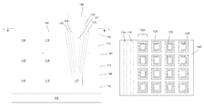
- FIGS. 1A-B are schematic diagrams illustrating cross sectional views of capacitors and nearby structures that are parts of an integrated circuit chip.
- FIGS. 2A-B are schematic diagrams illustrating cross sectional views of additional capacitor structures and nearby structures that are parts of an integrated circuit chip.
- FIG. 3 describes a method for making a capacitor that is part of an IC device.
- FIG. 4 describes an additional method for making a capacitor that is part of an IC device.
- FIG. 5 is a computing device built in accordance with an implementation of the invention.
- the proximate metal-containing and or high-k etchstop layer is a dense or highly dense dielectric layer.
- the proximate dense or ultra dense etch stop layer covers metal lines that are proximate to the capacitor during capacitor fabrication and remains in the IC device after fabrication.
- FIG. 1A illustrates a capacitor structure that is a part of an integrated circuit chip.
- the capacitor is, for example, a MIM (metal-insulator-metal) capacitor.
- the components shown in FIG. 1A represent a very small section of a typical IC device.
- a substrate 105 houses insulating layers 110 - 112 comprising metal-filled trenches 115 - 117 .
- Insulating layers 110 - 112 comprise an insulating material, such as, for example, silicon dioxide, silicon nitride, carbon doped oxide (CDO), silicon oxynitride, organic polymers such as perfluorocyclobutane or polytetrafluoroethylene, fluorosilicate glass (FSG), and organosilicates such as silsesquioxane, siloxane, and or organosilicate glass.
- Metal trenches 115 - 117 are typically the conducting lines that interconnect, the devices that form the IC chip.
- Metal-filled trenches 115 - 116 are optional parts of an IC device comprising capacitor 120 , and other numbers and configuration of metal trenches are possible.
- metal line 117 electrically connects capacitor 120 to other components of a monolithic IC device.
- the electrical interconnect that couples to a first end of capacitor 120 can be a via (not shown) that extends into substrate 105 electrically connecting capacitor 120 with other IC elements or devices (not shown).
- Metal lines 115 - 117 are comprised of, for example, copper, aluminum, silver, gold, platinum, or other conductive elements, or alloys thereof. In an embodiment of the invention, the metal lines 115 - 117 are comprised of copper.
- Capacitor 120 is formed in a well formed through insulating layers 111 - 112 .
- Capacitor 120 comprises an outer conducting layer 125 , an insulating layer 130 , and an inner conducting region 135 .
- the insulating layer 130 is disposed between the outer conducting layer 125 and the inner conducting region 135 .
- the outer metal layer 125 and the inner conducting region 135 comprise, for example, a metal such as tantalum, tantalum nitride, titanium, titanium nitride, tungsten, or other conductive materials, and or alloys thereof.
- the inner conducting region 130 can comprise one or more layers of conducting material (not shown), such as, a layer of tantalum proximate to the dielectric layer 130 and a metal fill comprised of copper that fills the remaining areas of the conducting region 135 .
- the insulating layer 130 is comprised, in embodiments of the invention, of a high-k material.
- High-k materials include materials, such as, for example, silicon oxy-mtride, hafnium oxide, zirconium oxide, hafnium silicate, hafnium oxynitride, lanthanum oxide, and or similar high dielectric constant materials.
- the insulating layer 130 can also be comprised of SiO 2 .
- conducting region 135 is a layer of conducting material within the conducting trench (as an alternative to a fill of conducting material) which is depicted by the dashed line within conducting region 135 .
- insulating region 137 is present and comprises a dielectric material. This alternative is depicted in FIG. 1A but not in FIG. 1B .
- Insulating layers 110 - 112 have dielectric etch stop layers 140 - 142 on at least one side.
- Etchstop layers 140 - 142 comprise an insulator, such as, for example, silicon nitride, silicon carbide, and silicon-carbon-nitride dielectric films.
- insulating layers 110 - 112 and etchstop layers 140 - 142 are films comprised of dielectric materials comprising at least 90% silicon, nitrogen, oxygen, and or carbon.
- Other configurations for insulating layers 110 - 112 and etchstop layers 140 - 142 are possible, such as, a single insulating layer comprised of layers 111 and 112 without the intervening etchstop layer 141 .
- a dense or ultradense etchstop layer 145 is provided in proximity to an end of capacitor 120 .
- the dense or ultradense etchstop layer 145 is provided on top of etchstop layer 142 during the fabrication of capacitor 120 .
- the dense or ultradense etchstop layer 145 can protect the proximate underlying metal lines 116 from damage.
- the dense or ultradense etchstop layer 145 remains in the device after fabrication has been completed.
- the dense or ultradense etchstop layer 145 is denser than the proximate etchstop layer 143 that is a film comprised of silicon, nitrogen, oxygen, and or carbon.
- the dense or ultradense etchstop layer 145 has a density that is greater than the density of etchstop layer 142 , that is greater than 3 g/cm 3 , greater than 4 g/cm 3 , or greater than 5 g/cm 3 , or in the range of 3 to 10 g/cm 3 , 4 to 10 g/cm 3 , or 5 to 10 g/cm 3 .
- the etchstop layer 143 is a lower density etchstop layer and has a density of, for example, 2 to 3 g/cm 3 .
- the dense or ultradense etchstop layer 145 has minimal dangling/broken bonds as compared to weakly more weakly bonded, lower-k etchstop layers.
- the dense or ultradense etchstop layer 145 is comprised of a high-k dielectric material.
- Useful high-k dielectric materials include transition metal oxides, such as, ZnO, HfO 2 , Al 2 O 3 , and TiO x (wherein x is greater than zero and less than 2).
- the dense or ultradense etchstop layer 145 is a dielectric material comprised of a transition metal.
- the dense or ultradense etchstop layer 145 can be a metal or transition metal oxide.
- the dense or ultradense etchstop layer 145 can be created, for example, using atomic vapor deposition processes. In embodiments of the invention the dense or ultradense etchstop layer 145 is 2-8 nm thick.
- capacitor 120 is part of a DRAM (dynamic random access memory) device or an eDRAM (embedded dynamic random access memory integrated on the same IC chip as ASIC (an application-specific integrated circuit) or a processor) and capacitor 120 is coupled to a transistor (not shown), typically through conducting line 117 , Because eDRAM cells are periodically refreshed, a memory controller is typically included in the IC chip.
- DRAM dynamic random access memory
- eDRAM embedded dynamic random access memory integrated on the same IC chip as ASIC (an application-specific integrated circuit) or a processor
- FIG. 1B is a view along 1 - 1 of the device of FIG. 1A and additionally includes an array of capacitors (whereas FIG. 1A only illustrated one capacitor). Although a 4 ⁇ 4 array of capacitors 120 are illustrated, other numbers and arrangements are also possible, and as in FIG. 1A , only a small portion of a full IC device is illustrated for clarity.
- capacitors 120 comprise an outer conducting layer 125 , an insulating layer 130 , and an inner conducting region 135 .
- the insulating layer 130 is disposed between the outer conducting layer 125 and the inner conducting region 135 .
- Metal trenches 116 are disposed in this view behind the dense or ultradense etchstop layer 145 , and are indicated with a dashed line.
- FIG. 2A illustrates an additional capacitor structure.
- the capacitor is, for example, a MIM (metal-insulator-metal) capacitor.
- the capacitor and other components shown in FIG. 2A are pan of an integrated circuit chip.
- the components shown in FIG. 2A represent a very small section of a typical IC device.
- a substrate 205 houses insulating layers 210 - 212 comprising metal trenches 215 - 217 .
- Insulating layers 210 - 212 comprise an insulating material, such as, for example, silicon dioxide, carbon doped oxide (CDO), silicon oxynitride, organic polymers such as perfluorocyclobutane or polytetrafluoroethylene, fluorosilicate glass (FSG), and organosilicates such as silsesquioxane, siloxane, and or organosilicate glass.
- Metal-filled trenches 215 - 217 are typically the conducting lines that interconnect the devices that form the IC chip.
- Metal-filled trenches 215 - 216 are optional parts of an IC device comprising capacitor 220 , and other numbers and configuration of metal trenches are possible.
- metal line 217 electrically connects capacitor 220 to other components of a monolithic IC device.
- the electrical interconnect that couples to a first end of capacitor 220 can be a via (not shown) that extends into substrate 205 electrically connecting capacitor 220 with other IC elements or devices.
- Metal lines 215 - 217 are comprised of, for example, copper, aluminum, silver, gold, platinum, or other conductive elements, or alloys thereof. In an embodiment of the invention, the metal lines 215 - 217 are comprised of copper.
- Capacitor 220 is formed in a well formed through insulating layers 211 - 212 .
- Capacitor 220 comprises an outer conducting layer 225 , an insulating layer 230 , and an inner conducting region 235 .
- the insulating layer 230 is disposed between the outer conducting layer 225 and the inner conducting region 235 .
- the outer conducting layer 225 is recessed within the well relative to the inner conducting layer 235 .
- the outer metal layer 225 and the inner conducting region 235 comprise, for example, a metal such as tantalum, tantalum nitride, titanium, titanium nitride, tungsten, or other conductive material, and or alloys or mixtures thereof.
- the inner conducting region 235 can comprise one or more layers of conducting material (not shown), such as, a layer of tantalum proximate to the dielectric layer 230 and a metal fill comprised of copper that fills the remaining areas of the conducting region 235 .
- the insulating layer 230 is comprised, in embodiments of the invention, of a high-k material.
- High-k materials include materials, such as, for example, silicon oxynitride, hafnium oxide, zirconium oxide, hafnium silicate, hafnium oxynitride, lanthanum oxide, and or similar high dielectric constant materials.
- the insulating layer 230 can also be comprised of SiO 2 .
- conducting region 235 is a layer of conducting material within the conducting trench (as an alternative to a fill of conducting material) which is depicted by the dashed line within conducting region 235 .
- insulating region 237 is present and comprises a dielectric material. This alternative is depicted in FIG. 2A but has been omitted from FIG. 2B for clarity of illustration.
- Insulating layers 210 - 212 have etch stop layers 240 - 242 on at least one side.
- Etchstop layers 240 - 242 comprise an insulator, such as, for example, silicon nitride, silicon carbide, and silicon-carbon-nitride dielectric films.
- insulating layers 210 - 212 and etchstop layers 240 - 242 are films comprised of dielectric materials comprising at least 90% silicon, nitrogen, oxygen, and or carbon.
- Other configurations for insulating layers 210 - 212 and etchstop layers 240 - 242 are possible, such as, a single insulating layer comprised of layers 211 and 212 without the intervening etchstop layer 241 .
- a dense or ultradense etchstop layer 245 is provided in proximity to an end of capacitor 220 .
- the dense or ultradense etchstop layer 245 is provided on top of etchstop layer 242 during the fabrication of capacitor 220 .
- the dense or ultradense etchstop layer 245 can protect the proximate underlying metal lines 216 from damage.
- the dense or ultradense etchstop layer 245 is proximate to the end of the capacitor 220 comprising the recessed area of outer conducting layer 225 .
- the dense or ultradense etchstop layer 245 remains in the device after fabrication has been completed.
- the dense or ultradense etchstop layer 245 is denser than the proximate etchstop layer 243 that is a film comprised of silicon, nitrogen, oxygen, and or carbon.
- the dense or ultradense etchstop layer 245 has a density that is greater than the density of etchstop layer 142 , that is greater than 3 g/cm 3 , greater than 4 g/cm 3 , or greater than 5 g/cm 3 , or in the range of 3 to 10 g/cm 3 , 4 to 10 g/cm 3 , or 5 to 10 g/cm 3 .
- the etchstop layer 143 is a lower density etchstop layer and has a density of, for example, 2 to 3 g/cm 3 .
- the dense or ultradense etchstop layer 145 has minimal dangling/broken bonds as compared to weakly more weakly bonded, lower-k etchstop layers.
- the dense or ultradense etchstop layer 245 is comprised of a high-k dielectric material.
- Useful high-k dielectric materials include transition metal oxides, such as, ZnO, HfO 3 , Al 2 O 3 , and TiO x (wherein x is greater than zero and less than 2).
- the dense or ultradense etchstop layer 245 is a dielectric material comprised of a transition metal.
- the dense or ultradense etchstop layer 245 can be a metal or transition metal oxide.
- the dense or ultradense etchstop layer 245 can be created, for example, using atomic vapor deposition processes. In embodiments of the invention the dense or ultradense etchstop layer 245 is 2-8 nm thick.
- the capacitor trench is created through these films and lands on an underlying metal line 217 (or 215 or other layer).
- the conductive bottom electrode 225 is deposited and the surface of the structure is polished to remove the excess bottom electrode material.
- a sacrificial material is deposited into the capacitor trench (such as a SLAM material (a sacrificial light absorbing material) and removed from the structure surface using a chemical mechanical polish (CMP) to stop on the bottom electrode 225 , and then a dry-etch is performed to recess the bottom electrode 225 .
- CMP chemical mechanical polish
- the SLAM can be comprised of a material having polymetric backbone.
- the SLAM can comprise a poly (norbornene) backbone which can includes a side group which can be modified to allow the modulation of the SLAM etch rate.
- the side group can be an aromatic or cage moiety (such as adamantyl) for decreasing the etch rate or a fluorine-containing moiety (such as —CR 3 or —C 2 F 5 ) for increasing the etch rate.
- the SLAM can also be comprised, for example of a siloxane-containing polymer material.
- capacitor 220 is part of a DRAM (dynamic random access memory) device or an eDRAM (embedded dynamic random access memory integrated on the same IC chip as ASIC (an application-specific integrated circuit) or a processor) and capacitor 220 is coupled to a transistor (not shown), typically through conducting line 217 . Because eDRAM cells are periodically refreshed, a memory controller is typically included in the IC chip housing the eDRAM cells.
- DRAM dynamic random access memory
- eDRAM embedded dynamic random access memory integrated on the same IC chip as ASIC (an application-specific integrated circuit) or a processor
- FIG. 2B is a view along 2 - 2 of the device of FIG. 2A and additionally includes an array of capacitors (whereas FIG. 2A illustrated one capacitor). Although a 4 ⁇ 4 array of capacitors 220 are illustrated, other numbers and arrangements are also possible, and as in FIG. 2A , only a small portion of a full IC device is illustrated for clarity.
- capacitors 220 comprise an outer conducting layer 225 (indicted by dotted lines), an insulating layer 230 , and an inner conducting region 235 .
- the insulating layer 230 covers the outer conducting layer 225 (which is indicated by dashed lines).
- Metal trenches 216 are disposed in this view behind the dense or ultradense etchstop layer 245 , and are indicated with a dashed line.
- FIG. 3 describes a process for constructing capacitors in IC chips according to embodiments of the invention.
- a substrate is provided that has at least one layer of insulating material and at least one metal-filled trench or via.
- a dense or ultradense etchstop layer as described herein is deposited on the insulating material or etchstop layer.
- the dense or ultradense etchstop layer is deposited by atomic vapor deposition.
- a well is then formed through the dense or ultradense etchstop layer and the optional conventional etchstop layer in the insulating material.
- the well makes contact with the at least one metal-filled trench or via.
- Layers of conducting material, insulating material, and conducting material are then sequentially deposited.
- the final conducting material is deposited at a thickness that fills the well.
- the surface of the substrate is then planarized down to the dense or ultradense etchstop layer leaving the dense or ultradense etchstop layer on the surface of the substrate.
- the substrate surface also comprises an outlet side of the capacitor structure that has been formed.
- the outlet side of the capacitor comprises a surface of the formed inner conducting region of the capacitor that is capable of making electrical contact with additional conducting regions (such as trenches or vias) that are subsequently formed on the substrate surface that comprises the dense or ultradense etchstop layer.
- additional conducting regions such as trenches or vias
- the substrate undergoes further processing to form additional structures on the substrate surface.
- FIG. 4 describes an additional process for constructing capacitors in IC chips according to embodiments of the invention.
- a substrate is provided that has at least one layer of insulating material and at least one metal-filled trench or via.
- additional metal-filled trenches or vias proximate to the surface of the insulating material.
- a dense or ultradense etchstop layer as described herein is deposited on the insulating material or etchstop layer.
- the dense or ultradense etchstop layer is deposited by atomic vapor deposition.
- a well is then formed through the dense or ultradense etchstop layer and the optional conventional etchstop layer in the insulating material.
- the well makes contact with the at least one metal-filled trench or via.
- a layer of conducting material is deposited on the substrate and the sides and bottom of the well.
- a sacrificial material (such as a SLAM) is then deposited into the well filling the well and the substrate surface is planarized removing the conducting material and the sacrificial material from the substrate surface, but not from the well.
- the sacrificial material and the conducting layer are then partially etched, recessing the sacrificial material and the conducting layer within the well.
- the dense or highly dense dielectric layer is capable of protecting proximate metal-filled trenches in an uppermost insulating layer during etching of the sacrificial material and conducting layer to recess them into the well.
- the sacrificial material is then removed from the well.
- Layer(s) insulating material and then conducting material are deposited.
- the final conducting material is deposited at a thickness that fills the well.
- the surface of the substrate is then planarized down to the dense or ultradense etchstop layer leaving the dense or ultradense etchstop layer on the surface.
- the outlet side of the capacitor structure that has been formed is also on the surface of the substrate.
- the outlet side of the capacitor comprises a surface of the formed inner conducting region of the capacitor that is capable of making electrical contact with additional conducting regions (such as trenches or vias) that are subsequently formed on the substrate surface that comprises the dense or ultradense etchstop layer.
- additional conducting regions such as trenches or vias
- the substrate undergoes further processing to form additional structures on the substrate surface.
- a high-k material is a material that has a dielectric constant greater than that of silicon dioxide.
- the dielectric constant of silicon dioxide is 3.9.
- Components of devices shown herein may comprise additional layers, such as liner and adhesion layers that separate layers comprising different materials, such as, for example, metal layers from insulating layers, and components illustrated as one layer for simplicity, can comprise a plurality of layers of the same or a different material depending, for example, on the manufacturing processes employed in constructing the device and the desired properties of the device.
- additional layers such as liner and adhesion layers that separate layers comprising different materials, such as, for example, metal layers from insulating layers, and components illustrated as one layer for simplicity, can comprise a plurality of layers of the same or a different material depending, for example, on the manufacturing processes employed in constructing the device and the desired properties of the device.
- Implementations of the invention are housed on a substrate, such as a semiconductor substrate.
- the substrate base on which semiconductor devices are built is typically a semiconductor wafer that is diced apart to yield individual IC chips.
- the base substrate on which an IC chip is built is typically a silicon wafer, although embodiments of the invention tire not dependent on the type of substrate used.
- the substrate could also be comprised of germanium, indium antimonide, lead telluride, indium arsenide, indium phosphide, gallium arsenide, gallium antimonide, and or other group III-V materials either alone or in combination with silicon or silicon dioxide or other insulating materials. Layers and layers comprising devices can also be described as the substrate or part of the substrate on which embodiments of the invention are housed or fabricated.
- FIG. 5 illustrates a computing device 1000 in accordance with one implementation of the invention.
- the computing device 1000 houses a motherboard 1002 .
- the motherboard 1002 may include a number of components, including but not limited to a processor 1004 and at least one communication chip 1006 .
- the processor 1004 is physically and electrically coupled to the motherboard 1002 .
- the at least one communication chip 1006 is also physically and electrically coupled to the motherboard 1002 .
- computing device 1000 may include other components that may or may not be physically and electrically coupled to the motherboard 1002 .
- these other components include, but are not limited to, volatile memory (e.g., DRAM), non-volatile memory (e.g., ROM), a graphics processor, a digital signal processor, a crypto processor, a chipset, an antenna, a display, a touchscreen display, a touchscreen controller, a battery, an audio codec, a video codec, a power amplifier, a global positioning system (GPS) device, a compass, an accelerometer, a gyroscope, a speaker, a camera, and a mass storage device (such as hard disk drive, compact disk (CD), digital versatile disk (DVD), and so forth).
- volatile memory e.g., DRAM
- non-volatile memory e.g., ROM
- graphics processor e.g., a digital signal processor
- a crypto processor e.g., a graphics processor
- the communication chip 1006 enables wireless communications for the transfer of data to and from the computing device 1000 .
- the term “wireless” and its derivatives may be used to describe circuits, devices, systems, methods, techniques, communications channels, etc., that may communicate data through the use of modulated electromagnetic radiation through a non-solid medium. The term does not imply that the associated devices do not contain any wires, although in some embodiments they might not.
- the communication chip 1006 may implement any of a number of wireless standards or protocols, including but not limited to Wi-Fi (IEEE 802.11 family), WIMAX (IEEE 802.16 family), IEEE 802.20, long term evolution (LIE), Ev-DO, HSPA+, HSDPA+, HSUPA+, EDGE, GSM, GPRS, CDMA, TDMA, DECT, Bluetooth, derivatives thereof, as well as any other wireless protocols that are designated as 3G, 4G, 5G, and beyond.
- the computing device 1000 may include a plurality of communication chips 1006 .
- a first communication chip 1006 may be dedicated to shorter range wireless communications such as Wi-Fi and Bluetooth and a second communication chip 1006 may be dedicated to longer range wireless communications such as GPS, EDGE, GPRS, CDMA, WiMAX, LTE, Ev-DO, and others.
- the processor 1004 of the computing device 1000 includes an integrated circuit die packaged within the processor 1004 .
- the integrated circuit die of the processor includes one or more devices, such as capactors, that are formed in accordance with implementations of the invention.
- the term “processor” may refer to any device or portion of a device that processes electronic data from registers and/or memory to transform that electronic data into other electronic data that may be stored in registers and/or memory.
- the communication chip 1006 also includes an integrated circuit die packaged within the communication chip 1006 .
- the integrated circuit die of the communication chip includes one or more devices, such as capacitors, DRAM, or eDRAM, that are formed in accordance with implementations of the invention.
- another component housed within the computing device 1000 may contain an integrated circuit die that includes one or more devices, such as capacitors, DRAM, or eDRAM that are formed in accordance with implementations of the invention.
- the computing device 1000 may be a laptop, a netbook, a notebook, a smartphone, a tablet, a personal digital assistant (PDA), an ultra mobile PC, a mobile phone, a desktop computer, a server, a printer, a scanner, a monitor, a set-top box, an entertainment control unit, a digital camera, a portable music player, or a digital video recorder.
- the computing device 1000 may be any other electronic device that processes data.
Abstract
Description
Claims (24)
Applications Claiming Priority (1)
| Application Number | Priority Date | Filing Date | Title |
|---|---|---|---|
| PCT/US2011/059192 WO2013066336A1 (en) | 2011-11-03 | 2011-11-03 | Etchstop layers and capacitors |
Related Parent Applications (1)
| Application Number | Title | Priority Date | Filing Date |
|---|---|---|---|
| PCT/US2011/059192 A-371-Of-International WO2013066336A1 (en) | 2011-11-03 | 2011-11-03 | Etchstop layers and capacitors |
Related Child Applications (1)
| Application Number | Title | Priority Date | Filing Date |
|---|---|---|---|
| US14/732,593 Continuation US9343524B2 (en) | 2011-11-03 | 2015-06-05 | Etchstop layers and capacitors |
Publications (2)
| Publication Number | Publication Date |
|---|---|
| US20130279102A1 US20130279102A1 (en) | 2013-10-24 |
| US9054068B2 true US9054068B2 (en) | 2015-06-09 |
Family
ID=48192520
Family Applications (4)
| Application Number | Title | Priority Date | Filing Date |
|---|---|---|---|
| US13/977,647 Active 2032-04-20 US9054068B2 (en) | 2011-11-03 | 2011-11-03 | Etchstop layers and capacitors |
| US14/732,593 Active US9343524B2 (en) | 2011-11-03 | 2015-06-05 | Etchstop layers and capacitors |
| US15/132,037 Active US9607992B2 (en) | 2011-11-03 | 2016-04-18 | Etchstop layers and capacitors |
| US15/428,087 Active US10032857B2 (en) | 2011-11-03 | 2017-02-08 | Etchstop layers and capacitors |
Family Applications After (3)
| Application Number | Title | Priority Date | Filing Date |
|---|---|---|---|
| US14/732,593 Active US9343524B2 (en) | 2011-11-03 | 2015-06-05 | Etchstop layers and capacitors |
| US15/132,037 Active US9607992B2 (en) | 2011-11-03 | 2016-04-18 | Etchstop layers and capacitors |
| US15/428,087 Active US10032857B2 (en) | 2011-11-03 | 2017-02-08 | Etchstop layers and capacitors |
Country Status (5)
| Country | Link |
|---|---|
| US (4) | US9054068B2 (en) |
| CN (1) | CN103907177B (en) |
| DE (1) | DE112011105805T5 (en) |
| TW (2) | TWI555083B (en) |
| WO (1) | WO2013066336A1 (en) |
Cited By (1)
| Publication number | Priority date | Publication date | Assignee | Title |
|---|---|---|---|---|
| US20150270331A1 (en) * | 2011-11-03 | 2015-09-24 | Intel Corporation | Etchstop layers and capacitors |
Families Citing this family (8)
| Publication number | Priority date | Publication date | Assignee | Title |
|---|---|---|---|---|
| US20170323955A1 (en) * | 2014-12-23 | 2017-11-09 | Intel Corporation | Apparatus and methods of forming fin structures with sidewall liner |
| US9627215B1 (en) * | 2015-09-25 | 2017-04-18 | Taiwan Semiconductor Manufacturing Company, Ltd. | Structure and method for interconnection |
| US20170287834A1 (en) * | 2016-03-29 | 2017-10-05 | Microchip Technology Incorporated | Contact Expose Etch Stop |
| US10283597B2 (en) * | 2016-11-10 | 2019-05-07 | The United States Of America, As Represented By The Secretary Of The Navy | Scandium-containing III-N etch-stop layers for selective etching of III-nitrides and related materials |
| US10276651B2 (en) | 2017-09-01 | 2019-04-30 | Taiwan Semiconductor Manufacturing Co., Ltd. | Low warpage high density trench capacitor |
| JP7178187B2 (en) * | 2018-06-27 | 2022-11-25 | 太陽誘電株式会社 | trench capacitor |
| DE102019118369B4 (en) | 2018-11-30 | 2023-10-12 | Taiwan Semiconductor Manufacturing Co. Ltd. | CAP STRUCTURE FOR TRENCH CAPACITORS AND METHOD FOR FORMING THE SAME |
| US11088239B2 (en) | 2018-11-30 | 2021-08-10 | Taiwan Semiconductor Manufacturing Company, Ltd. | Cap structure for trench capacitors |
Citations (14)
| Publication number | Priority date | Publication date | Assignee | Title |
|---|---|---|---|---|
| US6048445A (en) | 1998-03-24 | 2000-04-11 | Intel Corporation | Method of forming a metal line utilizing electroplating |
| US6365514B1 (en) | 1997-12-23 | 2002-04-02 | Intel Corporation | Two chamber metal reflow process |
| US6461955B1 (en) * | 1999-04-29 | 2002-10-08 | Texas Instruments Incorporated | Yield improvement of dual damascene fabrication through oxide filling |
| US6774037B2 (en) | 2002-05-17 | 2004-08-10 | Intel Corporation | Method integrating polymeric interlayer dielectric in integrated circuits |
| US6958547B2 (en) | 2002-05-03 | 2005-10-25 | Intel Corporation | Interconnect structures containing conductive electrolessly deposited etch stop layers, liner layers, and via plugs |
| US20060024950A1 (en) * | 2004-08-02 | 2006-02-02 | Suk-Hun Choi | Methods of forming metal contact structures and methods of fabricating phase-change memory devices using the same |
| US20060154436A1 (en) | 2004-12-03 | 2006-07-13 | Samsung Electronics Co., Ltd. | Metal-insulator-metal capacitor and a fabricating method thereof |
| US20060163730A1 (en) | 2003-04-08 | 2006-07-27 | Susumu Matsumoto | Electronic device and its manufacturing method |
| US20070059913A1 (en) | 2005-09-15 | 2007-03-15 | King Sean W | Capping layer to reduce amine poisoning of photoresist layers |
| US20080132030A1 (en) | 2006-12-05 | 2008-06-05 | Samsung Electronics Co., Ltd. | Method of manufacturing semiconductor device |
| US7812455B2 (en) | 2008-06-16 | 2010-10-12 | Intel Corporation | Interconnect in low-k interlayer dielectrics |
| US8058177B2 (en) | 2008-07-31 | 2011-11-15 | Intel Corporation | Winged vias to increase overlay margin |
| WO2013066336A1 (en) | 2011-11-03 | 2013-05-10 | Intel Corporation | Etchstop layers and capacitors |
| US20140002976A1 (en) | 2011-11-10 | 2014-01-02 | Ruth A. Brain | Recessed bottom-electrode capacitors and methods of assembling same |
Family Cites Families (10)
| Publication number | Priority date | Publication date | Assignee | Title |
|---|---|---|---|---|
| CN1201386C (en) * | 2001-08-22 | 2005-05-11 | 联华电子股份有限公司 | Embedding process of making metal capacitor and its product |
| CN1202569C (en) * | 2002-01-09 | 2005-05-18 | 中芯国际集成电路制造(上海)有限公司 | Method for forming capacitor for metel-insulation-metal structure in process of insertting copper |
| KR100549951B1 (en) | 2004-01-09 | 2006-02-07 | 삼성전자주식회사 | method for forming capacitor used to etching stopper layer for use in semiconductor memory |
| CN2800353Y (en) | 2005-06-03 | 2006-07-26 | 鸿富锦精密工业(深圳)有限公司 | Holder of computer case |
| US7846832B2 (en) * | 2005-07-07 | 2010-12-07 | Taiwan Semiconductor Manufacturing Co., Ltd. | Semiconductor device and fabrication method thereof |
| US20070290333A1 (en) * | 2006-06-16 | 2007-12-20 | Intel Corporation | Chip stack with a higher power chip on the outside of the stack |
| US8062971B2 (en) * | 2008-03-19 | 2011-11-22 | Infineon Technologies Ag | Dual damascene process |
| US8441097B2 (en) * | 2009-12-23 | 2013-05-14 | Intel Corporation | Methods to form memory devices having a capacitor with a recessed electrode |
| US8039920B1 (en) * | 2010-11-17 | 2011-10-18 | Intel Corporation | Methods for forming planarized hermetic barrier layers and structures formed thereby |
| US9773719B2 (en) * | 2012-11-26 | 2017-09-26 | Infineon Technologies Dresden Gmbh | Semiconductor packages and methods of fabrication thereof |
-
2011
- 2011-11-03 DE DE112011105805.5T patent/DE112011105805T5/en not_active Withdrawn
- 2011-11-03 WO PCT/US2011/059192 patent/WO2013066336A1/en active Application Filing
- 2011-11-03 CN CN201180074601.1A patent/CN103907177B/en active Active
- 2011-11-03 US US13/977,647 patent/US9054068B2/en active Active
-
2012
- 2012-11-02 TW TW101140773A patent/TWI555083B/en active
- 2012-11-02 TW TW105127886A patent/TWI616950B/en active
-
2015
- 2015-06-05 US US14/732,593 patent/US9343524B2/en active Active
-
2016
- 2016-04-18 US US15/132,037 patent/US9607992B2/en active Active
-
2017
- 2017-02-08 US US15/428,087 patent/US10032857B2/en active Active
Patent Citations (16)
| Publication number | Priority date | Publication date | Assignee | Title |
|---|---|---|---|---|
| US6365514B1 (en) | 1997-12-23 | 2002-04-02 | Intel Corporation | Two chamber metal reflow process |
| US6048445A (en) | 1998-03-24 | 2000-04-11 | Intel Corporation | Method of forming a metal line utilizing electroplating |
| US6461955B1 (en) * | 1999-04-29 | 2002-10-08 | Texas Instruments Incorporated | Yield improvement of dual damascene fabrication through oxide filling |
| US7008872B2 (en) | 2002-05-03 | 2006-03-07 | Intel Corporation | Use of conductive electrolessly deposited etch stop layers, liner layers and via plugs in interconnect structures |
| US6958547B2 (en) | 2002-05-03 | 2005-10-25 | Intel Corporation | Interconnect structures containing conductive electrolessly deposited etch stop layers, liner layers, and via plugs |
| US6774037B2 (en) | 2002-05-17 | 2004-08-10 | Intel Corporation | Method integrating polymeric interlayer dielectric in integrated circuits |
| US20060163730A1 (en) | 2003-04-08 | 2006-07-27 | Susumu Matsumoto | Electronic device and its manufacturing method |
| US20060024950A1 (en) * | 2004-08-02 | 2006-02-02 | Suk-Hun Choi | Methods of forming metal contact structures and methods of fabricating phase-change memory devices using the same |
| US20060154436A1 (en) | 2004-12-03 | 2006-07-13 | Samsung Electronics Co., Ltd. | Metal-insulator-metal capacitor and a fabricating method thereof |
| US20070059913A1 (en) | 2005-09-15 | 2007-03-15 | King Sean W | Capping layer to reduce amine poisoning of photoresist layers |
| US20080132030A1 (en) | 2006-12-05 | 2008-06-05 | Samsung Electronics Co., Ltd. | Method of manufacturing semiconductor device |
| US7812455B2 (en) | 2008-06-16 | 2010-10-12 | Intel Corporation | Interconnect in low-k interlayer dielectrics |
| US8143159B2 (en) | 2008-06-16 | 2012-03-27 | Intel Corporation | Fabrication of interconnects in a low-k interlayer dielectrics |
| US8058177B2 (en) | 2008-07-31 | 2011-11-15 | Intel Corporation | Winged vias to increase overlay margin |
| WO2013066336A1 (en) | 2011-11-03 | 2013-05-10 | Intel Corporation | Etchstop layers and capacitors |
| US20140002976A1 (en) | 2011-11-10 | 2014-01-02 | Ruth A. Brain | Recessed bottom-electrode capacitors and methods of assembling same |
Non-Patent Citations (3)
| Title |
|---|
| International Preliminary Report on Patentability received for PCT Patent Application No. PCT/US2011/059192, mailed on May 15, 2014, 4 pages. |
| International Search Report and Written Opinion received for International Application No. PCT/US2011/059192, mailed on Jul. 30, 2012, 9 pages. |
| Ruth Brain et al., U.S. Appl. No. 13/997,974, entitled "Recessed Bottom-Electrode Capacitors and Methods of Assembling Same," filed Jun. 25, 2013. |
Cited By (2)
| Publication number | Priority date | Publication date | Assignee | Title |
|---|---|---|---|---|
| US20150270331A1 (en) * | 2011-11-03 | 2015-09-24 | Intel Corporation | Etchstop layers and capacitors |
| US9343524B2 (en) * | 2011-11-03 | 2016-05-17 | Intel Corporation | Etchstop layers and capacitors |
Also Published As
| Publication number | Publication date |
|---|---|
| US20170148867A1 (en) | 2017-05-25 |
| US9343524B2 (en) | 2016-05-17 |
| US10032857B2 (en) | 2018-07-24 |
| US9607992B2 (en) | 2017-03-28 |
| US20130279102A1 (en) | 2013-10-24 |
| US20160233217A1 (en) | 2016-08-11 |
| CN103907177B (en) | 2016-08-31 |
| WO2013066336A1 (en) | 2013-05-10 |
| TWI616950B (en) | 2018-03-01 |
| DE112011105805T5 (en) | 2014-08-28 |
| US20150270331A1 (en) | 2015-09-24 |
| TW201338038A (en) | 2013-09-16 |
| CN103907177A (en) | 2014-07-02 |
| TW201714216A (en) | 2017-04-16 |
| TWI555083B (en) | 2016-10-21 |
Similar Documents
| Publication | Publication Date | Title |
|---|---|---|
| US10032857B2 (en) | Etchstop layers and capacitors | |
| US9691839B2 (en) | Metal-insulator-metal (MIM) capacitor with insulator stack having a plurality of metal oxide layers | |
| US10483160B2 (en) | Ultra thin helmet dielectric layer for maskless air gap and replacement ILD processes | |
| KR102304791B1 (en) | Optimizing gate profile for performance and gate fill | |
| US11653487B2 (en) | 4F2 DRAM cell using vertical thin film transistor | |
| TW201732947A (en) | Fabrication of non-planar IGZO devices for improved electrostatics | |
| US11723188B2 (en) | Replacement metal COB integration process for embedded DRAM | |
| KR102351550B1 (en) | Apparatus and methods of forming fin structures with sidewall liner | |
| US20210125992A1 (en) | Interconnect structures for integrated circuits | |
| US11690215B2 (en) | Self-aligned bitline and capacitor via formation | |
| US20210366821A1 (en) | Through plate interconnect for a vertical mim capacitor | |
| US20200212055A1 (en) | Integration scheme for ferroelectric memory with a deep trench structure | |
| US11605592B2 (en) | Method to fabricate metal and ferromagnetic metal multilayer interconnect line for skin effect suppression | |
| US20160225715A1 (en) | Microelectronic transistor contacts and methods of fabricating the same | |
| US20170077389A1 (en) | Embedded memory in interconnect stack on silicon die | |
| US20210098373A1 (en) | Integrated circuit structures having differentiated interconnect lines in a same dielectric layer | |
| US20200303381A1 (en) | Nonvolatile static random access memory (sram) devices | |
| WO2019009873A1 (en) | Damascene patterning for thin-film transistor fabrication | |
| WO2019009872A1 (en) | Self-aligned back-gate top-contact thin-film transistor |
Legal Events
| Date | Code | Title | Description |
|---|---|---|---|
| AS | Assignment |
Owner name: INTEL CORPORATION, CALIFORNIA Free format text: ASSIGNMENT OF ASSIGNORS INTEREST;ASSIGNOR:BRAIN, RUTH A.;REEL/FRAME:027172/0001 Effective date: 20111101 |
|
| FEPP | Fee payment procedure |
Free format text: PAYOR NUMBER ASSIGNED (ORIGINAL EVENT CODE: ASPN); ENTITY STATUS OF PATENT OWNER: LARGE ENTITY |
|
| STCF | Information on status: patent grant |
Free format text: PATENTED CASE |
|
| MAFP | Maintenance fee payment |
Free format text: PAYMENT OF MAINTENANCE FEE, 4TH YEAR, LARGE ENTITY (ORIGINAL EVENT CODE: M1551); ENTITY STATUS OF PATENT OWNER: LARGE ENTITY Year of fee payment: 4 |
|
| AS | Assignment |
Owner name: TAHOE RESEARCH, LTD., IRELAND Free format text: ASSIGNMENT OF ASSIGNORS INTEREST;ASSIGNOR:INTEL CORPORATION;REEL/FRAME:061175/0176 Effective date: 20220718 |
|
| MAFP | Maintenance fee payment |
Free format text: PAYMENT OF MAINTENANCE FEE, 8TH YEAR, LARGE ENTITY (ORIGINAL EVENT CODE: M1552); ENTITY STATUS OF PATENT OWNER: LARGE ENTITY Year of fee payment: 8 |