US9040966B2 - Method for producing organic transistor, organic transistor, method for producing semiconductor device, semiconductor device, and electronic apparatus - Google Patents
Method for producing organic transistor, organic transistor, method for producing semiconductor device, semiconductor device, and electronic apparatus Download PDFInfo
- Publication number
- US9040966B2 US9040966B2 US13/981,721 US201213981721A US9040966B2 US 9040966 B2 US9040966 B2 US 9040966B2 US 201213981721 A US201213981721 A US 201213981721A US 9040966 B2 US9040966 B2 US 9040966B2
- Authority
- US
- United States
- Prior art keywords
- general formula
- alkyl group
- compound represented
- compound
- insulating film
- Prior art date
- Legal status (The legal status is an assumption and is not a legal conclusion. Google has not performed a legal analysis and makes no representation as to the accuracy of the status listed.)
- Expired - Fee Related
Links
- 239000004065 semiconductor Substances 0.000 title claims abstract description 169
- 238000004519 manufacturing process Methods 0.000 title description 19
- 150000001875 compounds Chemical class 0.000 claims abstract description 264
- 125000000217 alkyl group Chemical group 0.000 claims abstract description 97
- 238000000034 method Methods 0.000 claims abstract description 61
- 229920000642 polymer Polymers 0.000 claims abstract description 55
- 125000001424 substituent group Chemical group 0.000 claims abstract description 53
- -1 poly(α-methylstyrene) Polymers 0.000 claims description 67
- 239000000758 substrate Substances 0.000 claims description 67
- 239000002994 raw material Substances 0.000 claims description 52
- 229920003251 poly(α-methylstyrene) Polymers 0.000 claims description 31
- 238000005191 phase separation Methods 0.000 claims description 21
- 230000002269 spontaneous effect Effects 0.000 claims description 19
- 239000002904 solvent Substances 0.000 claims description 14
- AUHZEENZYGFFBQ-UHFFFAOYSA-N mesitylene Substances CC1=CC(C)=CC(C)=C1 AUHZEENZYGFFBQ-UHFFFAOYSA-N 0.000 claims description 13
- 125000001827 mesitylenyl group Chemical group [H]C1=C(C(*)=C(C([H])=C1C([H])([H])[H])C([H])([H])[H])C([H])([H])[H] 0.000 claims description 13
- RFFLAFLAYFXFSW-UHFFFAOYSA-N 1,2-dichlorobenzene Chemical compound ClC1=CC=CC=C1Cl RFFLAFLAYFXFSW-UHFFFAOYSA-N 0.000 claims description 10
- UHOVQNZJYSORNB-UHFFFAOYSA-N Benzene Chemical compound C1=CC=CC=C1 UHOVQNZJYSORNB-UHFFFAOYSA-N 0.000 claims description 6
- YXFVVABEGXRONW-UHFFFAOYSA-N Toluene Chemical compound CC1=CC=CC=C1 YXFVVABEGXRONW-UHFFFAOYSA-N 0.000 claims description 6
- CXWXQJXEFPUFDZ-UHFFFAOYSA-N tetralin Chemical compound C1=CC=C2CCCCC2=C1 CXWXQJXEFPUFDZ-UHFFFAOYSA-N 0.000 claims description 6
- 229920001577 copolymer Polymers 0.000 claims description 5
- URLKBWYHVLBVBO-UHFFFAOYSA-N Para-Xylene Chemical group CC1=CC=C(C)C=C1 URLKBWYHVLBVBO-UHFFFAOYSA-N 0.000 claims description 4
- RDOXTESZEPMUJZ-UHFFFAOYSA-N anisole Chemical compound COC1=CC=CC=C1 RDOXTESZEPMUJZ-UHFFFAOYSA-N 0.000 claims description 4
- IIEWJVIFRVWJOD-UHFFFAOYSA-N ethylcyclohexane Chemical compound CCC1CCCCC1 IIEWJVIFRVWJOD-UHFFFAOYSA-N 0.000 claims description 4
- XDTMQSROBMDMFD-UHFFFAOYSA-N Cyclohexane Chemical compound C1CCCCC1 XDTMQSROBMDMFD-UHFFFAOYSA-N 0.000 claims description 2
- CTQNGGLPUBDAKN-UHFFFAOYSA-N O-Xylene Chemical compound CC1=CC=CC=C1C CTQNGGLPUBDAKN-UHFFFAOYSA-N 0.000 claims description 2
- UZKWTJUDCOPSNM-UHFFFAOYSA-N methoxybenzene Substances CCCCOC=C UZKWTJUDCOPSNM-UHFFFAOYSA-N 0.000 claims description 2
- 239000008096 xylene Substances 0.000 claims description 2
- 239000010408 film Substances 0.000 description 232
- 239000000243 solution Substances 0.000 description 58
- 0 *C1=CC=C(C2=C3C=CC4=C5C3=C(C=C2)OC2=C5C3=C(C=CC(C5=CC=C(*)C=C5)=C3C=C2)O4)C=C1.*C1=CC=CC(C2=C3C=CC4=C5C3=C(C=C2)OC2=C5C3=C(C=CC(C5=CC(*)=CC=C5)=C3C=C2)O4)=C1.*C1=CC=CC=C1C1=C2C=CC3=C4C2=C(C=C1)OC1=C4C2=C(C=CC(C4=CC=CC=C4*)=C2C=C1)O3 Chemical compound *C1=CC=C(C2=C3C=CC4=C5C3=C(C=C2)OC2=C5C3=C(C=CC(C5=CC=C(*)C=C5)=C3C=C2)O4)C=C1.*C1=CC=CC(C2=C3C=CC4=C5C3=C(C=C2)OC2=C5C3=C(C=CC(C5=CC(*)=CC=C5)=C3C=C2)O4)=C1.*C1=CC=CC=C1C1=C2C=CC3=C4C2=C(C=C1)OC1=C4C2=C(C=CC(C4=CC=CC=C4*)=C2C=C1)O3 0.000 description 53
- 239000000463 material Substances 0.000 description 35
- 238000000576 coating method Methods 0.000 description 32
- 239000011248 coating agent Substances 0.000 description 30
- 239000003990 capacitor Substances 0.000 description 18
- 239000012299 nitrogen atmosphere Substances 0.000 description 11
- 229910052751 metal Inorganic materials 0.000 description 9
- TZNSPLMKPZQANF-UHFFFAOYSA-N C1=CC2=C3C(=C1)C=CC1=C3C3=C(C=CC4=CC=CC(=C43)O1)O2.CC.CC.CC.CC Chemical compound C1=CC2=C3C(=C1)C=CC1=C3C3=C(C=CC4=CC=CC(=C43)O1)O2.CC.CC.CC.CC TZNSPLMKPZQANF-UHFFFAOYSA-N 0.000 description 8
- 239000002184 metal Substances 0.000 description 8
- 238000009751 slip forming Methods 0.000 description 7
- 238000001035 drying Methods 0.000 description 6
- 230000005669 field effect Effects 0.000 description 6
- 238000004770 highest occupied molecular orbital Methods 0.000 description 6
- 238000007639 printing Methods 0.000 description 6
- 230000008569 process Effects 0.000 description 6
- 239000012298 atmosphere Substances 0.000 description 5
- 230000000052 comparative effect Effects 0.000 description 5
- 238000000151 deposition Methods 0.000 description 5
- 229920001665 Poly-4-vinylphenol Polymers 0.000 description 4
- 229910045601 alloy Inorganic materials 0.000 description 4
- 239000000956 alloy Substances 0.000 description 4
- MWPLVEDNUUSJAV-UHFFFAOYSA-N anthracene Chemical compound C1=CC=CC2=CC3=CC=CC=C3C=C21 MWPLVEDNUUSJAV-UHFFFAOYSA-N 0.000 description 4
- 239000011651 chromium Substances 0.000 description 4
- 239000010931 gold Substances 0.000 description 4
- 238000005259 measurement Methods 0.000 description 4
- PXHVJJICTQNCMI-UHFFFAOYSA-N Nickel Chemical compound [Ni] PXHVJJICTQNCMI-UHFFFAOYSA-N 0.000 description 3
- KDLHZDBZIXYQEI-UHFFFAOYSA-N Palladium Chemical compound [Pd] KDLHZDBZIXYQEI-UHFFFAOYSA-N 0.000 description 3
- XUIMIQQOPSSXEZ-UHFFFAOYSA-N Silicon Chemical compound [Si] XUIMIQQOPSSXEZ-UHFFFAOYSA-N 0.000 description 3
- QVGXLLKOCUKJST-UHFFFAOYSA-N atomic oxygen Chemical compound [O] QVGXLLKOCUKJST-UHFFFAOYSA-N 0.000 description 3
- AMDQVKPUZIXQFC-UHFFFAOYSA-N dinaphthylene dioxide Chemical compound O1C(C2=C34)=CC=CC2=CC=C3OC2=CC=CC3=CC=C1C4=C32 AMDQVKPUZIXQFC-UHFFFAOYSA-N 0.000 description 3
- 238000002347 injection Methods 0.000 description 3
- 239000007924 injection Substances 0.000 description 3
- 150000002739 metals Chemical class 0.000 description 3
- 239000001301 oxygen Substances 0.000 description 3
- 229910052760 oxygen Inorganic materials 0.000 description 3
- 229920003023 plastic Polymers 0.000 description 3
- 239000004033 plastic Substances 0.000 description 3
- BASFCYQUMIYNBI-UHFFFAOYSA-N platinum Chemical compound [Pt] BASFCYQUMIYNBI-UHFFFAOYSA-N 0.000 description 3
- 229910052710 silicon Inorganic materials 0.000 description 3
- 239000010703 silicon Substances 0.000 description 3
- WKBPZYKAUNRMKP-UHFFFAOYSA-N 1-[2-(2,4-dichlorophenyl)pentyl]1,2,4-triazole Chemical compound C=1C=C(Cl)C=C(Cl)C=1C(CCC)CN1C=NC=N1 WKBPZYKAUNRMKP-UHFFFAOYSA-N 0.000 description 2
- KGVZFKPXHUHYIQ-UHFFFAOYSA-N CC(C)CC1=CC=C(C2=C3C=CC4=C5C3=C(C=C2)OC2=C\5C3=C(C=CC(C5=CC=C(CC(C)C)C=C5)=C3\C=C/2)O4)C=C1.CCC1=CC=C(C2=C3C=CC4=C5C3=C(C=C2)OC2=C\5C3=C(C=CC(C5=CC=C(CC)C=C5)=C3\C=C/2)O4)C=C1.CCCC1=CC=C(C2=C3C=CC4=C5C3=C(C=C2)OC2=C\5C3=C(C=CC(C5=CC=C(CCC)C=C5)=C3\C=C/2)O4)C=C1.CCCCC1=CC=C(C2=C3C=CC4=C5C3=C(C=C2)OC2=C\5C3=C(C=CC(C5=CC=C(CCCC)C=C5)=C3\C=C/2)O4)C=C1.CCCCCC1=CC=C(C2=C3C=CC4=C5C3=C(C=C2)OC2=C\5C3=C(C=CC(C5=CC=C(CCCCC)C=C5)=C3\C=C/2)O4)C=C1.CCCCCCC1=CC=C(C2=C3C=CC4=C5C3=C(C=C2)OC2=C\5C3=C(C=CC(C5=CC=C(CCCCCC)C=C5)=C3\C=C/2)O4)C=C1.CCCCCCCC1=CC=C(C2=C3C=CC4=C5C3=C(C=C2)OC2=C\5C3=C(C=CC(C5=CC=C(CCCCCCC)C=C5)=C3\C=C/2)O4)C=C1 Chemical compound CC(C)CC1=CC=C(C2=C3C=CC4=C5C3=C(C=C2)OC2=C\5C3=C(C=CC(C5=CC=C(CC(C)C)C=C5)=C3\C=C/2)O4)C=C1.CCC1=CC=C(C2=C3C=CC4=C5C3=C(C=C2)OC2=C\5C3=C(C=CC(C5=CC=C(CC)C=C5)=C3\C=C/2)O4)C=C1.CCCC1=CC=C(C2=C3C=CC4=C5C3=C(C=C2)OC2=C\5C3=C(C=CC(C5=CC=C(CCC)C=C5)=C3\C=C/2)O4)C=C1.CCCCC1=CC=C(C2=C3C=CC4=C5C3=C(C=C2)OC2=C\5C3=C(C=CC(C5=CC=C(CCCC)C=C5)=C3\C=C/2)O4)C=C1.CCCCCC1=CC=C(C2=C3C=CC4=C5C3=C(C=C2)OC2=C\5C3=C(C=CC(C5=CC=C(CCCCC)C=C5)=C3\C=C/2)O4)C=C1.CCCCCCC1=CC=C(C2=C3C=CC4=C5C3=C(C=C2)OC2=C\5C3=C(C=CC(C5=CC=C(CCCCCC)C=C5)=C3\C=C/2)O4)C=C1.CCCCCCCC1=CC=C(C2=C3C=CC4=C5C3=C(C=C2)OC2=C\5C3=C(C=CC(C5=CC=C(CCCCCCC)C=C5)=C3\C=C/2)O4)C=C1 KGVZFKPXHUHYIQ-UHFFFAOYSA-N 0.000 description 2
- SDYJHGRDVLRDHB-UHFFFAOYSA-N CC(C)CCC1=CC=C(C2=C3C=CC4=C5C3=C(C=C2)OC2=C\5C3=C(C=CC(C5=CC=C(CCC(C)C)C=C5)=C3\C=C/2)O4)C=C1.CC(C)CCCC1=CC=C(C2=C3C=CC4=C5C3=C(C=C2)OC2=C\5C3=C(C=CC(C5=CC=C(CCCC(C)C)C=C5)=C3\C=C/2)O4)C=C1 Chemical compound CC(C)CCC1=CC=C(C2=C3C=CC4=C5C3=C(C=C2)OC2=C\5C3=C(C=CC(C5=CC=C(CCC(C)C)C=C5)=C3\C=C/2)O4)C=C1.CC(C)CCCC1=CC=C(C2=C3C=CC4=C5C3=C(C=C2)OC2=C\5C3=C(C=CC(C5=CC=C(CCCC(C)C)C=C5)=C3\C=C/2)O4)C=C1 SDYJHGRDVLRDHB-UHFFFAOYSA-N 0.000 description 2
- VYZAMTAEIAYCRO-UHFFFAOYSA-N Chromium Chemical compound [Cr] VYZAMTAEIAYCRO-UHFFFAOYSA-N 0.000 description 2
- 229920001609 Poly(3,4-ethylenedioxythiophene) Polymers 0.000 description 2
- 239000004372 Polyvinyl alcohol Substances 0.000 description 2
- 229910021417 amorphous silicon Inorganic materials 0.000 description 2
- 230000005540 biological transmission Effects 0.000 description 2
- 229910052804 chromium Inorganic materials 0.000 description 2
- 239000010949 copper Substances 0.000 description 2
- 230000000694 effects Effects 0.000 description 2
- 238000005530 etching Methods 0.000 description 2
- 239000011521 glass Substances 0.000 description 2
- PCHJSUWPFVWCPO-UHFFFAOYSA-N gold Chemical compound [Au] PCHJSUWPFVWCPO-UHFFFAOYSA-N 0.000 description 2
- 229910052737 gold Inorganic materials 0.000 description 2
- 238000010438 heat treatment Methods 0.000 description 2
- 230000006872 improvement Effects 0.000 description 2
- 238000002156 mixing Methods 0.000 description 2
- 238000007645 offset printing Methods 0.000 description 2
- 239000002245 particle Substances 0.000 description 2
- 229920003229 poly(methyl methacrylate) Polymers 0.000 description 2
- 229920000139 polyethylene terephthalate Polymers 0.000 description 2
- 239000005020 polyethylene terephthalate Substances 0.000 description 2
- 239000004926 polymethyl methacrylate Substances 0.000 description 2
- 229920002451 polyvinyl alcohol Polymers 0.000 description 2
- 239000010936 titanium Substances 0.000 description 2
- XLYOFNOQVPJJNP-UHFFFAOYSA-N water Substances O XLYOFNOQVPJJNP-UHFFFAOYSA-N 0.000 description 2
- 229920003026 Acene Polymers 0.000 description 1
- LFLHAGJAUFMTKK-UHFFFAOYSA-N C.C.CCCC1C2CCC(C2)C1C Chemical compound C.C.CCCC1C2CCC(C2)C1C LFLHAGJAUFMTKK-UHFFFAOYSA-N 0.000 description 1
- RCBMZGYOJYDBLU-WXUKJITCSA-N CCCCCC/C=C/C1=C2C=CC3=C4C2=C(C=C1)OC1=C4C2=C(C=CC(/C=C/CCCCCC)=C2C=C1)O3 Chemical compound CCCCCC/C=C/C1=C2C=CC3=C4C2=C(C=C1)OC1=C4C2=C(C=CC(/C=C/CCCCCC)=C2C=C1)O3 RCBMZGYOJYDBLU-WXUKJITCSA-N 0.000 description 1
- VITOYURJANJRAI-FLFKKZLDSA-N CCCCCC1=CC=C(/C=C/C2=C3C=CC4=C5C3=C(C=C2)OC2=C5C3=C(C=CC(/C=C/C5=CC=C(CCCCC)C=C5)=C3C=C2)O4)C=C1 Chemical compound CCCCCC1=CC=C(/C=C/C2=C3C=CC4=C5C3=C(C=C2)OC2=C5C3=C(C=CC(/C=C/C5=CC=C(CCCCC)C=C5)=C3C=C2)O4)C=C1 VITOYURJANJRAI-FLFKKZLDSA-N 0.000 description 1
- RYGMFSIKBFXOCR-UHFFFAOYSA-N Copper Chemical compound [Cu] RYGMFSIKBFXOCR-UHFFFAOYSA-N 0.000 description 1
- YTPLMLYBLZKORZ-UHFFFAOYSA-N Divinylene sulfide Natural products C=1C=CSC=1 YTPLMLYBLZKORZ-UHFFFAOYSA-N 0.000 description 1
- ZOKXTWBITQBERF-UHFFFAOYSA-N Molybdenum Chemical compound [Mo] ZOKXTWBITQBERF-UHFFFAOYSA-N 0.000 description 1
- YPXYRDNJBMDECS-UHFFFAOYSA-N Nc(cccc1)c1-c(cc1)c(cc2)c3c1Oc(cc1)c4-c3c2Oc(cc2)c4c1c2-c(cccc1)c1N Chemical compound Nc(cccc1)c1-c(cc1)c(cc2)c3c1Oc(cc1)c4-c3c2Oc(cc2)c4c1c2-c(cccc1)c1N YPXYRDNJBMDECS-UHFFFAOYSA-N 0.000 description 1
- 229920012266 Poly(ether sulfone) PES Polymers 0.000 description 1
- 239000004642 Polyimide Substances 0.000 description 1
- BQCADISMDOOEFD-UHFFFAOYSA-N Silver Chemical compound [Ag] BQCADISMDOOEFD-UHFFFAOYSA-N 0.000 description 1
- ATJFFYVFTNAWJD-UHFFFAOYSA-N Tin Chemical compound [Sn] ATJFFYVFTNAWJD-UHFFFAOYSA-N 0.000 description 1
- RTAQQCXQSZGOHL-UHFFFAOYSA-N Titanium Chemical compound [Ti] RTAQQCXQSZGOHL-UHFFFAOYSA-N 0.000 description 1
- 229910052782 aluminium Inorganic materials 0.000 description 1
- XAGFODPZIPBFFR-UHFFFAOYSA-N aluminium Chemical compound [Al] XAGFODPZIPBFFR-UHFFFAOYSA-N 0.000 description 1
- 230000004888 barrier function Effects 0.000 description 1
- 238000005452 bending Methods 0.000 description 1
- QPNAZOXLNBQYJS-UHFFFAOYSA-N c(cc1)ccc1-c(cc1)c2Oc3ccc(cc4)c5c3-c3c2c1ccc3Oc5c4-c1ccccc1 Chemical compound c(cc1)ccc1-c(cc1)c2Oc3ccc(cc4)c5c3-c3c2c1ccc3Oc5c4-c1ccccc1 QPNAZOXLNBQYJS-UHFFFAOYSA-N 0.000 description 1
- NQSXCTZMCODKGP-UHFFFAOYSA-N c(cc1)ccc1-c1cc(c2c3-4)ccc3Oc3cc(-c5ccccc5)cc(cc5)c3c-4c5Oc2c1 Chemical compound c(cc1)ccc1-c1cc(c2c3-4)ccc3Oc3cc(-c5ccccc5)cc(cc5)c3c-4c5Oc2c1 NQSXCTZMCODKGP-UHFFFAOYSA-N 0.000 description 1
- 229920001940 conductive polymer Polymers 0.000 description 1
- 239000004020 conductor Substances 0.000 description 1
- 229910052802 copper Inorganic materials 0.000 description 1
- 230000008021 deposition Effects 0.000 description 1
- 238000013461 design Methods 0.000 description 1
- 238000011161 development Methods 0.000 description 1
- 238000007598 dipping method Methods 0.000 description 1
- 239000007772 electrode material Substances 0.000 description 1
- 238000005401 electroluminescence Methods 0.000 description 1
- 238000005516 engineering process Methods 0.000 description 1
- 238000007646 gravure printing Methods 0.000 description 1
- 239000012535 impurity Substances 0.000 description 1
- 229910052738 indium Inorganic materials 0.000 description 1
- APFVFJFRJDLVQX-UHFFFAOYSA-N indium atom Chemical compound [In] APFVFJFRJDLVQX-UHFFFAOYSA-N 0.000 description 1
- 238000007641 inkjet printing Methods 0.000 description 1
- 239000012212 insulator Substances 0.000 description 1
- 239000004973 liquid crystal related substance Substances 0.000 description 1
- 230000014759 maintenance of location Effects 0.000 description 1
- 239000010445 mica Substances 0.000 description 1
- 229910052618 mica group Inorganic materials 0.000 description 1
- 238000012986 modification Methods 0.000 description 1
- 230000004048 modification Effects 0.000 description 1
- 229910052750 molybdenum Inorganic materials 0.000 description 1
- 239000011733 molybdenum Substances 0.000 description 1
- 229910052759 nickel Inorganic materials 0.000 description 1
- 239000011368 organic material Substances 0.000 description 1
- 229920000620 organic polymer Polymers 0.000 description 1
- 229910052763 palladium Inorganic materials 0.000 description 1
- SLIUAWYAILUBJU-UHFFFAOYSA-N pentacene Chemical compound C1=CC=CC2=CC3=CC4=CC5=CC=CC=C5C=C4C=C3C=C21 SLIUAWYAILUBJU-UHFFFAOYSA-N 0.000 description 1
- 150000002964 pentacenes Chemical class 0.000 description 1
- 229910052697 platinum Inorganic materials 0.000 description 1
- 229920000172 poly(styrenesulfonic acid) Polymers 0.000 description 1
- 239000004417 polycarbonate Substances 0.000 description 1
- 229920000515 polycarbonate Polymers 0.000 description 1
- 229910021420 polycrystalline silicon Inorganic materials 0.000 description 1
- 239000011112 polyethylene naphthalate Substances 0.000 description 1
- 229920001721 polyimide Polymers 0.000 description 1
- 229920002959 polymer blend Polymers 0.000 description 1
- 229920006254 polymer film Polymers 0.000 description 1
- 229920005591 polysilicon Polymers 0.000 description 1
- 229940005642 polystyrene sulfonic acid Drugs 0.000 description 1
- 239000010453 quartz Substances 0.000 description 1
- 238000007650 screen-printing Methods 0.000 description 1
- VYPSYNLAJGMNEJ-UHFFFAOYSA-N silicon dioxide Inorganic materials O=[Si]=O VYPSYNLAJGMNEJ-UHFFFAOYSA-N 0.000 description 1
- 229910052709 silver Inorganic materials 0.000 description 1
- 239000004332 silver Substances 0.000 description 1
- 238000004528 spin coating Methods 0.000 description 1
- 239000007921 spray Substances 0.000 description 1
- 239000010935 stainless steel Substances 0.000 description 1
- 229910001220 stainless steel Inorganic materials 0.000 description 1
- 229910052715 tantalum Inorganic materials 0.000 description 1
- GUVRBAGPIYLISA-UHFFFAOYSA-N tantalum atom Chemical compound [Ta] GUVRBAGPIYLISA-UHFFFAOYSA-N 0.000 description 1
- 239000010409 thin film Substances 0.000 description 1
- 229930192474 thiophene Natural products 0.000 description 1
- 229910052719 titanium Inorganic materials 0.000 description 1
- 238000012546 transfer Methods 0.000 description 1
- 239000012780 transparent material Substances 0.000 description 1
- WFKWXMTUELFFGS-UHFFFAOYSA-N tungsten Chemical compound [W] WFKWXMTUELFFGS-UHFFFAOYSA-N 0.000 description 1
- 229910052721 tungsten Inorganic materials 0.000 description 1
- 239000010937 tungsten Substances 0.000 description 1
Images


Classifications
-
- H01L51/005—
-
- C—CHEMISTRY; METALLURGY
- C07—ORGANIC CHEMISTRY
- C07D—HETEROCYCLIC COMPOUNDS
- C07D493/00—Heterocyclic compounds containing oxygen atoms as the only ring hetero atoms in the condensed system
- C07D493/02—Heterocyclic compounds containing oxygen atoms as the only ring hetero atoms in the condensed system in which the condensed system contains two hetero rings
- C07D493/06—Peri-condensed systems
-
- H01L51/0058—
-
- H—ELECTRICITY
- H10—SEMICONDUCTOR DEVICES; ELECTRIC SOLID-STATE DEVICES NOT OTHERWISE PROVIDED FOR
- H10K—ORGANIC ELECTRIC SOLID-STATE DEVICES
- H10K10/00—Organic devices specially adapted for rectifying, amplifying, oscillating or switching; Organic capacitors or resistors having potential barriers
- H10K10/40—Organic transistors
- H10K10/46—Field-effect transistors, e.g. organic thin-film transistors [OTFT]
- H10K10/462—Insulated gate field-effect transistors [IGFETs]
- H10K10/466—Lateral bottom-gate IGFETs comprising only a single gate
-
- H—ELECTRICITY
- H10—SEMICONDUCTOR DEVICES; ELECTRIC SOLID-STATE DEVICES NOT OTHERWISE PROVIDED FOR
- H10K—ORGANIC ELECTRIC SOLID-STATE DEVICES
- H10K10/00—Organic devices specially adapted for rectifying, amplifying, oscillating or switching; Organic capacitors or resistors having potential barriers
- H10K10/40—Organic transistors
- H10K10/46—Field-effect transistors, e.g. organic thin-film transistors [OTFT]
- H10K10/462—Insulated gate field-effect transistors [IGFETs]
- H10K10/468—Insulated gate field-effect transistors [IGFETs] characterised by the gate dielectrics
- H10K10/471—Insulated gate field-effect transistors [IGFETs] characterised by the gate dielectrics the gate dielectric comprising only organic materials
-
- H—ELECTRICITY
- H10—SEMICONDUCTOR DEVICES; ELECTRIC SOLID-STATE DEVICES NOT OTHERWISE PROVIDED FOR
- H10K—ORGANIC ELECTRIC SOLID-STATE DEVICES
- H10K10/00—Organic devices specially adapted for rectifying, amplifying, oscillating or switching; Organic capacitors or resistors having potential barriers
- H10K10/40—Organic transistors
- H10K10/46—Field-effect transistors, e.g. organic thin-film transistors [OTFT]
- H10K10/462—Insulated gate field-effect transistors [IGFETs]
- H10K10/468—Insulated gate field-effect transistors [IGFETs] characterised by the gate dielectrics
- H10K10/474—Insulated gate field-effect transistors [IGFETs] characterised by the gate dielectrics the gate dielectric comprising a multilayered structure
-
- H—ELECTRICITY
- H10—SEMICONDUCTOR DEVICES; ELECTRIC SOLID-STATE DEVICES NOT OTHERWISE PROVIDED FOR
- H10K—ORGANIC ELECTRIC SOLID-STATE DEVICES
- H10K71/00—Manufacture or treatment specially adapted for the organic devices covered by this subclass
- H10K71/10—Deposition of organic active material
- H10K71/12—Deposition of organic active material using liquid deposition, e.g. spin coating
-
- H—ELECTRICITY
- H10—SEMICONDUCTOR DEVICES; ELECTRIC SOLID-STATE DEVICES NOT OTHERWISE PROVIDED FOR
- H10K—ORGANIC ELECTRIC SOLID-STATE DEVICES
- H10K85/00—Organic materials used in the body or electrodes of devices covered by this subclass
- H10K85/60—Organic compounds having low molecular weight
- H10K85/615—Polycyclic condensed aromatic hydrocarbons, e.g. anthracene
- H10K85/626—Polycyclic condensed aromatic hydrocarbons, e.g. anthracene containing more than one polycyclic condensed aromatic rings, e.g. bis-anthracene
-
- H—ELECTRICITY
- H10—SEMICONDUCTOR DEVICES; ELECTRIC SOLID-STATE DEVICES NOT OTHERWISE PROVIDED FOR
- H10K—ORGANIC ELECTRIC SOLID-STATE DEVICES
- H10K85/00—Organic materials used in the body or electrodes of devices covered by this subclass
- H10K85/60—Organic compounds having low molecular weight
- H10K85/649—Aromatic compounds comprising a hetero atom
- H10K85/657—Polycyclic condensed heteroaromatic hydrocarbons
- H10K85/6574—Polycyclic condensed heteroaromatic hydrocarbons comprising only oxygen in the heteroaromatic polycondensed ring system, e.g. cumarine dyes
-
- H01L51/0545—
Definitions
- the present disclosure relates to a method for producing an organic transistor, an organic transistor, a method for producing a semiconductor device, a semiconductor device, and an electronic apparatus. More specifically, the present disclosure relates to a method for producing an organic transistor using a dioxaanthanthrene-based compound, an organic transistor, a method for producing a semiconductor device, a semiconductor device, and an electronic apparatus using the organic transistor or the semiconductor device.
- an active layer (a semiconductor film) in a semiconductor device such as a field effect transistor, an inorganic-based semiconductor material represented by silicon is used.
- the semiconductor device using the semiconductor film formed of the inorganic-based semiconductor material such as silicon has disadvantages as follows. Firstly, since a vacuum process, a high-temperature heat treatment, or the like is necessary, a large amount of energy is consumed. Secondly, since a high-temperature heat treatment is necessary, a type of substrate to be used is limited. Thirdly, investment in an expensive facility for fabrication is necessary. Fourthly, since the inorganic-based semiconductor material is hard and brittle, durability for bending or tensile stress is low.
- a semiconductor device including a semiconductor film formed of an organic semiconductor material has received attention.
- the semiconductor device has advantages as follows, as compared with a semiconductor device using a semiconductor film formed of an inorganic-based semiconductor material. Firstly, the semiconductor film can be formed at a low temperature. Secondly, since the organic semiconductor material is soluble in a solvent, the semiconductor film can be formed by coating. Thirdly, since the organic semiconductor material is soluble in a solvent, the semiconductor film can be formed by a printing method. Fourthly, since the semiconductor film can be easily formed by a coating or printing method, it has advantageous in terms of an increase in an area of the semiconductor film.
- the semiconductor film can be formed at a low temperature, the semiconductor film can be formed on a flexible substrate which has low heat resistance, but is flexible, which is formed of a plastic, or the like, and thus a flexible semiconductor device can be fabricated.
- characteristics of the semiconductor film can be controlled through substituent control of the organic semiconductor material, multiple functions and high performance of a semiconductor device can be attempted.
- low costs of a semiconductor device can be attempted.
- carrier mobility of the field effect transistor is equal to or less than 0.1 cm 2 V ⁇ 1 s ⁇ 1 , and is smaller than 1 cm 2 V ⁇ 1 s ⁇ 1 , which is mobility of a field effect transistor (a thin film transistor) using amorphous silicon of the related art.
- the organic semiconductor material has a problem related to carrier injection. That is, in general, it is said that in organic molecules, a molecule having a shallow HOMO (highest occupied molecular orbital) is unstable. In fact, in polyacene compounds, it is said that since anthracene having a short ring length has a deeper HOMO than pentacene having a long ring length, anthracene is stable.
- the organic semiconductor material is unstable in the atmosphere or at a high temperature, as compared with the inorganic semiconductor material. That is, as described above, an organic molecule, which is capable of satisfactory performing carrier injection on an electrode, has a shallow HOMO, but the organic molecule is likely to be unstable in the atmosphere or at a high temperature. Further, it is known that the organic semiconductor material is decomposed through a reaction of its own material to oxygen. Based these reasons, it is known that characteristics of the semiconductor device using the semiconductor film formed of the organic semiconductor material are deteriorated.
- a dioxaanthanthrene-based compound such as 6,12-dioxaanthanthrene (also known as peri xanthenoxanthene, 6,12-dioxaanthanthrene (may be abbreviated as “PXX”)) as the organic semiconductor material (see Non-Patent Literature 1 and Patent Literature 1).
- PXX dioxaanthanthrene-based compound
- the above-described problems caused in the case in which the semiconductor film formed of the organic semiconductor material is used can be solved.
- PXX is stable in the atmosphere and has excellent heat resistance (see Non-Patent Literature 1).
- the organic semiconductor film is formed using the above-described dioxaanthanthrene-based compound
- the organic semiconductor film is formed on a gate insulating film after the gate insulating film is formed, or a gate insulating film is formed on the organic semiconductor film after the organic semiconductor film using the dioxaanthanthrene-based compound is formed, it is difficult to form a satisfactory interface between the organic semiconductor film and the gate insulating film. Therefore, it is difficult to obtain sufficiently high carrier mobility in the organic transistor.
- a semiconductor device such as an organic transistor, and a method for producing the same capable of obtaining sufficiently high carrier mobility.
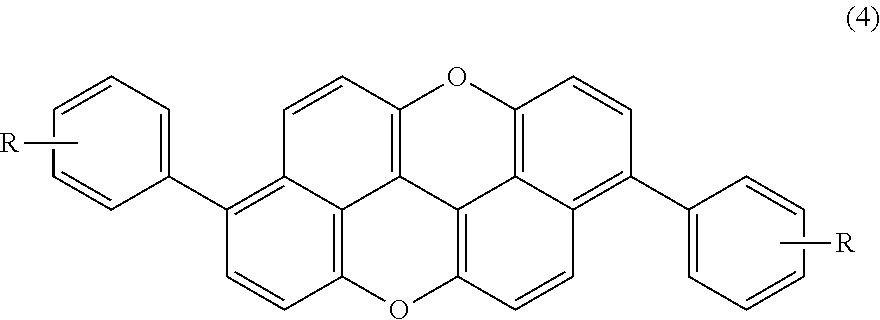
- a method of producing an organic transistor including collectively forming a gate insulating film and an organic semiconductor film by applying, onto a gate electrode disposed on a base substrate, a solution including a polymer and at least one compound of a compound represented by General Formula 1, a compound represented by General Formula 2, a compound represented by General Formula 3, a compound represented by General Formula 4, a compound having a structure represented by General Formula 4, in which R is a substituent other than an alkyl group, a compound represented by General Formula 5, a compound represented by General Formula 6, a compound having a structure represented by General Formula 5 or 6, in which R is a substituent other than an alkyl group, and a compound represented by General Formula 7, the gate insulating film containing the polymer, the organic semiconductor film being formed on the gate insulating film and containing the at least one compound, and forming a source electrode and a drain electrode on the organic semiconductor film.
- R is an alkyl group, and a number of R's is 2 to 5)
- R is an alkyl group, and a number of R's is 1 to 5)
- R is an alkyl group, and a number of R's is 1 to 5)
- R is an alkyl group or another substituent, and a number of R's is 1 to 5)
- an organic transistor including a gate insulating film and an organic semiconductor film collectively formed by applying, onto a gate electrode disposed on a base substrate, a solution including a polymer and at least one compound of a compound represented by General Formula 1, a compound represented by General Formula 2, a compound represented by General Formula 3, a compound represented by General Formula 4, a compound having a structure represented by General Formula 4, in which R is a substituent other than an alkyl group, a compound represented by General Formula 5, a compound represented by General Formula 6, a compound having a structure represented by General Formula 5 or 6, in which R is a substituent other than an alkyl group, and a compound represented by General Formula 7, the gate insulating film containing the polymer, the organic semiconductor film being formed on the gate insulating film and containing the at least one compound, and a source electrode and a drain electrode disposed on the organic semiconductor film.
- an electronic apparatus including an organic transistor which includes a gate insulating film and an organic semiconductor film collectively formed by applying, onto a gate electrode disposed on a base substrate, a solution including a polymer and at least one compound of a compound represented by General Formula 1, a compound represented by General Formula 2, a compound represented by General Formula 3, a compound represented by General Formula 4, a compound having a structure represented by General Formula 4, in which R is a substituent other than an alkyl group, a compound represented by General Formula 5, a compound represented by General Formula 6, a compound having a structure represented by General Formula 5 or 6, in which R is a substituent other than an alkyl group, and a compound represented by General Formula 7, the gate insulating film containing the polymer, the organic semiconductor film being formed on the gate insulating film and containing the at least one compound, and a source electrode and a drain electrode disposed on the organic semiconductor film.
- a method of producing a semiconductor device including collectively forming an insulating film and an organic semiconductor film by applying, onto a base substrate, a solution including a polymer and at least one compound of a compound represented by General Formula 1, a compound represented by General Formula 2, a compound represented by General Formula 3, a compound represented by General Formula 4, a compound having a structure represented by General Formula 4, in which R is a substituent other than an alkyl group, a compound represented by General Formula 5, a compound represented by General Formula 6, a compound having a structure represented by General Formula 5 or 6, in which R is a substituent other than an alkyl group, and a compound represented by General Formula 7, the insulating film containing the polymer, and the organic semiconductor film formed on the insulating film and containing the at least one compound.
- a semiconductor device including an insulating film and an organic semiconductor film collectively formed by applying, onto a base substrate, a solution including a polymer and at least one compound of a compound represented by General Formula 1, a compound represented by General Formula 2, a compound represented by General Formula 3, a compound represented by General Formula 4, a compound having a structure represented by General Formula 4, in which R is a substituent other than an alkyl group, a compound represented by General Formula 5, a compound represented by General Formula 6, a compound having a structure represented by General Formula 5 or 6, in which R is a substituent other than an alkyl group, and a compound represented by General Formula 7, the insulating film containing the polymer, the organic semiconductor film being formed on the insulating film and containing the at least one compound.
- an electronic apparatus including a semiconductor device which includes an insulating film and an organic semiconductor film collectively formed by applying, onto a base substrate, a solution including a polymer and at least one compound of a compound represented by General Formula 1, a compound represented by General Formula 2, a compound represented by General Formula 3, a compound represented by General Formula 4, a compound having a structure represented by General Formula 4, in which R is a substituent other than an alkyl group, a compound represented by General Formula 5, a compound represented by General Formula 6, a compound having a structure represented by General Formula 5 or 6, in which R is a substituent other than an alkyl group, and a compound represented by General Formula 7, the insulating film containing the polymer, the organic semiconductor film formed on the insulating film and containing the at least one compound.
- the at least one compound is one compound represented by the following Formulas 9 to 17.
- the gate insulating film and the organic semiconductor film may be formed by forming an organic insulating film
- an insulating polymer capable of forming an insulating film may be used, preferably, at least one of poly( ⁇ -methylstyrene) and a cycloolefin copolymer may be used, but the polymer is not limited thereto.
- a solvent of the solution conventionally known solvents may be used, and the solvent is selected as needed.
- the solvent is at least one among xylene, p-xylene, mesitylene, toluene, tetralin, anisole, benzene, 1,2-dichlorobenzene, o-dichlorobenzene, cyclohexane, and ethyl cyclohexane.
- a dry condition (temperature, time, and the like) of the solution is appropriately selected according to the used solvent.
- the semiconductor device may have basically all structures.
- the semiconductor device includes the organic transistor having a structure in which an organic semiconductor film and a gate insulating film are disposed to be in contact with each other, but for example, the semiconductor device may include a capacitor having a structure in which an insulating film is interposed between an organic semiconductor film and another conductive film (for example, an organic semiconductor film, a metal film, or the like).
- the electronic apparatus may be a variety of electronic apparatuses using an organic transistor or a semiconductor device, and may include both a portable electronic apparatus and a stationary electronic apparatus, and a function or use thereof is not used.
- specific examples of the electronic apparatus may include a display such as a liquid crystal display or an organic electroluminescence display, a portable phone, a mobile apparatus, a personal computer, a game machine, car equipment, a household electrical appliance, an industrial product, and the like.
- a gate insulating film and insulating film containing the polymer and an organic semiconductor film continuously formed with the gate insulating film or insulating film on the gate insulating film or insulating film and containing the at least one compound are obtained by applying a solution including a polymer and at least one compound among a compound represented by General Formula 1, a compound represented by General Formula 2, a compound represented by General Formula 3, a compound represented by General Formula 4, a compound having a structure represented by General Formula 4, in which R is a substituent other than an alkyl group, a compound represented by General Formula 5, a compound represented by General Formula 6, a compound having a structure represented by General Formula 5 or 6, in which R is a substituent other than an alkyl group, and a compound represented by General Formula 7, a satisfactory interface between an organic semiconductor film and a gate insulating film or a satisfactory interface between the organic semiconductor film and an insulating film can be simply obtained.
- an organic transistor in which carrier scattering in the interface between the organic semiconductor film and the gate insulating film does not occur and which has sufficiently high carrier mobility can be obtained.
- a semiconductor device such as an organic transistor having sufficiently high carrier mobility or a capacitor having satisfactory characteristics can be obtained.
- an organic semiconductor film including at least one compound among a compound represented by General Formula 1, a compound represented by General Formula 2, a compound represented by General Formula 3, a compound represented by General Formula 4, a compound having a structure represented by General Formula 4, in which R is a substituent other than an alkyl group, a compound represented by General Formula 5, a compound represented by General Formula 6, a compound having a structure represented by General Formula 5 or 6, in which R is a substituent other than an alkyl group, and a compound represented by General Formula 7.
- a high-performance electronic apparatus can be realized by using the excellent organic transistor or semiconductor device.
- FIG. 1 is a cross-sectional view illustrating an organic transistor according to a first embodiment.
- FIG. 2A is a cross-sectional view illustrating a method for producing the organic transistor according to the first embodiment.
- FIG. 2B is a cross-sectional view illustrating a method for producing the organic transistor according to the first embodiment.
- FIG. 3 is a figure-substitute photograph illustrating a cross-sectional transmission electron microscope photograph of an example of a laminated structure of an organic semiconductor film and the insulating polymer film formed by phase-separation from a raw material solution.
- FIG. 4 is a cross-sectional view illustrating a capacitor according to a second embodiment.
- FIG. 5A is a cross-sectional view illustrating a method producing the capacitor according to the second embodiment.
- FIG. 5B is a cross-sectional view illustrating a method for producing the capacitor according to the second embodiment.
- FIG. 1 illustrates an organic transistor according to a first embodiment.
- a gate electrode 12 is disposed on a substrate 11 .
- a gate insulating film 13 is disposed to cover the gate electrode 12 .
- the gate insulating film 13 has a double-layered structure of an insulating film 13 a and an insulating film 13 b formed thereon.
- An organic semiconductor film 14 which is a channel region is disposed on the gate insulating film 13 .
- a source electrode 15 and a drain electrode 16 are disposed on the organic semiconductor film 14 .
- a top-contact bottom-gate organic transistor having a configuration of an insulated gate field effect transistor is constituted by the gate electrode 12 , the organic film 14 , the source electrode 15 , and the drain electrode 16 .
- the organic semiconductor film 14 includes at least one compound among a compound represented by General Formula 1, a compound represented by General Formula 2, a compound represented by General Formula 3, a compound represented by General Formula 4, a compound having a structure represented by General Formula 4, in which R is a substituent other than an alkyl group, a compound represented by General Formula 5, a compound represented by General Formula 6, a compound having a structure represented by General Formula 5 or 6, in which R is a substituent other than an alkyl group, and a compound represented by General Formula 7, preferably, a compound of any one represented by Formulas 9 to 17.
- a lower-layered insulating film 13 a of the gate insulating film 13 includes, for example, an organic insulator such as PVP-RSiCl 3 , DAP, or isoDAP.
- an upper-layered insulating film 13 b of the gate insulating film 13 is selected, for example, from among previously mentioned polymers as necessary.
- the polymer preferably, at least one of poly( ⁇ -methylstyrene) and a cycloolefin copolymer may be used.
- the cycloolefin copolymer TOPAS (registered trademark) (manufactured by TOPAS ADVANCED POLYMERS GmbH) represented by the following structural formula may be used.
- the organic semiconductor film 14 and the upper-layered insulating film 13 b of the gate insulating film 13 are continuously formed in a thickness direction thereof. Thicknesses of the gate insulating film 13 and the organic semiconductor film 14 are appropriately selected according to characteristics necessary for the organic transistor.
- a material of the substrate 11 is selected from among conventionally known materials as necessary, and may be a transparent material or a material opaque to visible light. Further, the substrate 11 may be conductive or non-conductive. The substrate 11 may be flexible or non-flexible. Specifically, examples of the material of the substrate 11 may include a variety of plastics (organic polymers) such as polymethyl methacrylate (PMMA), polyvinyl alcohol (PVA), polyvinyl phenol (PVP), polyether sulfone (PES), polyimide, polycarbonate, polyethylene terephthalate (PET), or polyethylene naphthalate (PEN), mica, a variety of glass substrates, a quartz substrate, a silicon substrate, a variety of alloys such as stainless steel, and a variety of metals.
- plastic organic polymers
- the substrate 11 may be made to be flexible, and thus, a flexible organic transistor may be obtained.
- Examples of a material containing the gate electrode 12 , the source electrode 15 , and the drain electrode 16 may include a metal such as platinum (Pt), gold (Au), palladium (Pd), chromium (Cr), molybdenum (Mo), nickel (Ni), aluminum (Al), silver (Ag), tantalum (Ta), tungsten (W), copper (Cu), titanium (Ti), indium (In), or tin (Sn), or a variety of conductive materials such as alloys containing the metal elements, conductive particles formed of the metals, conductive particles formed of the alloys containing the metals, and polysilicon containing impurities.
- a metal such as platinum (Pt), gold (Au), palladium (Pd), chromium (Cr), molybdenum (Mo), nickel (Ni), aluminum (Al), silver (Ag), tantalum (Ta), tungsten (W), copper (Cu), titanium (Ti), indium (In), or tin (
- Examples of the material containing the gate electrode 12 , the source electrode 15 , and the drain electrode 16 may include organic materials (conductive polymers) such as poly(3,4-ethylenedioxythiophene)/polystyrene sulfonic acid (PEDOT/PSS).
- the gate electrode 12 , the source electrode 15 , and the drain electrode 16 may have a laminated structure of two or more kinds of layers made of the.
- a width (a gate length) of the gate electrode 12 in a length direction of a channel or a distance (a channel length) between the source electrode 15 and the drain electrode 16 is appropriately selected according to characteristics and the like necessary for the organic transistor.
- FIGS. 2A and 2B illustrate a method for producing the organic transistor.
- a gate electrode 12 is formed on a substrate 11 , and an insulating film 13 a is thereon.
- a solvent of the raw material solution is appropriately selected from among the previously mentioned solvents. Further, a mixing ratio (a mass ratio or a weight ratio) of the compound and the insulating polymer in the raw material solution is selected as necessary.
- the raw material solution 17 prepared in this way is coated or printed on the insulating film 13 a in a film shape.
- the coating method of the raw material solution 17 may include a spin coat method and the like.
- the printing method of a raw material solution 18 may include a screen printing method, an inkjet printing method, an offset printing method, a reverse offset printing method, a gravure printing method, a microcontact method, and the like.
- Examples of a coating or printing method of the raw material solution 17 may include a variety of coating methods such as an air doctor coater method, a blade coater method, a rod coater method, a knife coater method, a squeeze coater method, a reverse roll coater method, a transfer roll coater method, a gravure coater method, a kiss coater method, a cast coater method, a spray coater method, a slit orifice coater method, a calendar coater method, and a dipping method.
- coating methods such as an air doctor coater method, a blade coater method, a rod coater method, a knife coater method, a squeeze coater method, a reverse roll coater method, a transfer roll coater method, a gravure coater method, a kiss coater method, a cast coater method, a spray coater method, a slit orifice coater method, a calendar coater method, and a dipping method.
- the film-shaped raw material solution 17 is dried.
- the at least one compound among the compound represented by General Formula 1, the compound represented by General Formula 2, the compound represented by General Formula 3, the compound represented by General Formula 4, the compound having a structure represented by General Formula 4, wherein R is a substituent other than an alkyl group, a compound represented by General Formula 5, the compound represented by General Formula 6, the compound having a structure represented by General Formula 5 or 6, wherein R is a substituent other than an alkyl group, and the compound represented by General Formula 7, and the insulating polymer contained in the raw material solution 17 are spontaneously phase-separated into layer shapes.
- an insulating film 13 b formed of the insulating polymer and an organic semiconductor film 14 formed thereon and formed of the compound are continuously formed in a thickness direction.
- the organic semiconductor film 14 formed in this way is patterned in a predetermined shape by etching or the like, and then a source electrode 16 and a drain electrode 17 are formed on the organic semiconductor film 14 by a conventionally known method.
- a raw material solution was prepared by uniformly dissolving a compound (abbreviated as C2Ph-PXX) represented by Formula 9 and poly( ⁇ -methylstyrene) (abbreviated as p- ⁇ MS), which is an insulating polymer, in mesitylene.
- C2Ph-PXX a compound represented by Formula 9
- p- ⁇ MS poly( ⁇ -methylstyrene)
- the raw material solution prepared in this way was coated on a substrate in which a gate electrode is formed by a spin coat method.
- a substrate a glass substrate of which a surface is covered with an organic insulating film containing cross-linked polyvinyl phenol (PVP) as a main component was used.
- PVP polyvinyl phenol
- FIG. 3 illustrates a cross-sectional transmission electron microscope photograph of a sample.
- the gate insulating film formed of poly( ⁇ -methylstyrene) and having a thickness of about 15 nm and the organic semiconductor film formed of C2Ph-PXX and having a thickness of about 10 nm formed thereon form a distinct interface and are continuously formed.
- a source electrode and a drain formed of gold (Au) were formed on the organic semiconductor film formed of C2Ph-PXX with a chromium (Cr) film interposed as an adhesion layer therebetween. In this way, a bottom gate organic transistor was produced.
- a raw material solution was prepared by uniformly dissolving a compound (abbreviated as C3Ph-PXX) represented by Formula 10 and poly( ⁇ -methylstyrene) (p- ⁇ MS), which is an insulating polymer, in mesitylene.
- C3Ph-PXX a compound represented by Formula 10
- p- ⁇ MS poly( ⁇ -methylstyrene)
- the raw material solution prepared in this way was coated on a substrate by a spin coat method.
- the same substrate as in Example 1 was used as the substrate.
- the coating film formed in this way was dried in a nitrogen atmosphere at 60° C. for 1 hour. Accordingly, spontaneous phase-separation was caused in the coating film, and a laminated structure of a gate insulating film formed of poly( ⁇ -methylstyrene) and an organic semiconductor film formed of C3Ph-PXX formed thereon was formed.
- a raw material solution was prepared by uniformly dissolving a compound (abbreviated as C4Ph-PXX) represented by Formula 11 and poly( ⁇ -methylstyrene) (p- ⁇ MS), which is an insulating polymer, in mesitylene.
- C4Ph-PXX a compound represented by Formula 11
- p- ⁇ MS poly( ⁇ -methylstyrene)
- the raw material solution prepared in this way was coated on a substrate by a spin coat method.
- the same substrate as Example 1 was used as the substrate.
- the coating film formed in this way was dried in a nitrogen atmosphere at 60° C. for 1 hour. Accordingly, spontaneous phase-separation was caused in the coating film, and a laminated structure of a gate insulating film formed of poly( ⁇ -methylstyrene) and an organic semiconductor film formed of C4Ph-PXX formed thereon was formed.
- a raw material solution was prepared by uniformly dissolving a compound (abbreviated as C5Ph-PXX) represented by Formula 12 and poly( ⁇ -methylstyrene) (p- ⁇ MS), which is an insulating polymer, in mesitylene.
- C5Ph-PXX a compound represented by Formula 12
- p- ⁇ MS poly( ⁇ -methylstyrene)
- the raw material solution prepared in this way was coated on a substrate by a spin coat method.
- the same substrate as Example 1 was used as the substrate.
- the coating film formed in this way was dried in a nitrogen atmosphere at 60° C. for 1 hour. Accordingly, spontaneous phase-separation was caused in the coating film, and a laminated structure of a gate insulating film formed of poly( ⁇ -methylstyrene) and an organic semiconductor film formed of C5Ph-PXX formed thereon was formed.
- a raw material solution was prepared by uniformly dissolving a compound (abbreviated as C6Ph-PXX) represented by Formula 13 and poly( ⁇ -methylstyrene) (p- ⁇ MS), which is an insulating polymer, in mesitylene.
- C6Ph-PXX a compound represented by Formula 13
- p- ⁇ MS poly( ⁇ -methylstyrene)
- the raw material solution prepared in this way was coated on a substrate by a spin coat method.
- the same substrate as Example 1 was used as the substrate.
- the coating film formed in this way was dried in a nitrogen atmosphere at 60° C. for 1 hour. Accordingly, spontaneous phase-separation was caused in the coating film, and a laminated structure of a gate insulating film formed of poly( ⁇ -methylstyrene) and an organic semiconductor film formed of C6Ph-PXX formed thereon was formed.
- a raw material solution was prepared by uniformly dissolving a compound (abbreviated as C9Ph-PXX) represented by Formula 14 and poly( ⁇ -methylstyrene) (p- ⁇ MS), which is an insulating polymer, in mesitylene.
- C9Ph-PXX a compound represented by Formula 14
- p- ⁇ MS poly( ⁇ -methylstyrene)
- the raw material solution prepared in this way was coated on a substrate by a spin coat method.
- the same substrate as Example 1 was used as the substrate.
- the coating film formed in this way was dried in a nitrogen atmosphere at 60° C. for 1 hour. Accordingly, spontaneous phase-separation was caused in the coating film, and a laminated structure of a gate insulating film formed of poly( ⁇ -methylstyrene) and an organic semiconductor film formed of C9Ph-PXX formed thereon was formed.
- a raw material solution was prepared by uniformly dissolving a compound (abbreviated as iC4Ph-PXX) represented by Formula 15 and poly( ⁇ -methylstyrene) (p- ⁇ MS), which is an insulating polymer, in mesitylene.
- iC4Ph-PXX a compound represented by Formula 15
- p- ⁇ MS poly( ⁇ -methylstyrene)
- the raw material solution prepared in this way was coated on a substrate by a spin coat method.
- the same substrate as Example 1 was used as the substrate.
- the coating film formed in this way was dried in a nitrogen atmosphere at 60° C. for 1 hour. Accordingly, spontaneous phase-separation was caused in the coating film, and a laminated structure of a gate insulating film formed of poly( ⁇ -methylstyrene) and an organic semiconductor film formed of iC4Ph-PXX formed thereon was formed.
- a raw material solution was prepared by uniformly dissolving a compound (abbreviated as iC5Ph-PXX) represented by Formula 16 and poly( ⁇ -methylstyrene) (p- ⁇ MS), which is an insulating polymer, in mesitylene.
- iC5Ph-PXX a compound represented by Formula 16
- p- ⁇ MS poly( ⁇ -methylstyrene)
- the raw material solution prepared in this way was coated on a substrate by a spin coat method.
- the same substrate as Example 1 was used as the substrate.
- the coating film formed in this way was dried in a nitrogen atmosphere at 60° C. for 1 hour. Accordingly, spontaneous phase-separation was caused in the coating film, and a laminated structure of a gate insulating film formed of poly( ⁇ -methylstyrene) and an organic semiconductor film formed of iC5Ph-PXX formed thereon was formed.
- a raw material solution was prepared by uniformly dissolving a compound (abbreviated as iC6Ph-PXX) represented by Formula 17 and poly( ⁇ -methylstyrene) (p- ⁇ MS), which is an insulating polymer, in mesitylene.
- iC6Ph-PXX a compound represented by Formula 17
- p- ⁇ MS poly( ⁇ -methylstyrene)
- the raw material solution prepared in this way was coated on a substrate by a spin coat method.
- the same substrate as Example 1 was used as the substrate.
- the coating film formed in this way was dried in a nitrogen atmosphere at 60° C. for 1 hour. Accordingly, spontaneous phase-separation was caused in the coating film, and a laminated structure of a gate insulating film formed of poly( ⁇ -methylstyrene) and an organic semiconductor film formed of iC6Ph-PXX formed thereon was formed.
- a raw material solution was prepared by uniformly dissolving a compound represented by the following Formula 19 and poly( ⁇ -methylstyrene) (p- ⁇ MS), which is an insulating polymer, in mesitylene.
- p- ⁇ MS poly( ⁇ -methylstyrene)
- the raw material solution prepared in this way was coated on a substrate by a spin coat method.
- the same substrate as Example 1 was used as the substrate.
- the coating film formed in this way was dried in a nitrogen atmosphere at 60° C. for 1 hour. Accordingly, spontaneous phase-separation was caused in the coating film, and a laminated structure of a gate insulating film formed of poly( ⁇ -methylstyrene) and an organic semiconductor film formed of the compound represented by Formula 19 formed thereon was formed.
- a raw material solution was prepared by uniformly dissolving a compound represented by the following Formula 20 and poly( ⁇ -methylstyrene) (p- ⁇ MS), which is an insulating polymer, in mesitylene.
- the raw material solution prepared in this way was coated on a substrate by a spin coat method.
- the same substrate as Example 1 was used as the substrate.
- the coating film formed in this way was dried in a nitrogen atmosphere at 60° C. for 1 hour. Accordingly, spontaneous phase-separation was caused in the coating film, and a laminated structure of a gate insulating film formed of poly( ⁇ -methylstyrene) and an organic semiconductor film formed of the compound represented by Formula 20 formed thereon was formed.
- Carrier mobility of the organic transistors of Examples 1 to 9 and Comparative Examples 1 and 2 was measured. Measurement results of the carrier mobility of the organic transistors of Examples 1 to 9 are shown in Table 1.
- organic transistors were produced by forming organic semiconductor films by vacuum depositing C2Ph-PXX, C3Ph-PXX, and 9Ph-PXX. Here, before the organic semiconductor films were formed, gate insulating films formed of poly( ⁇ -methylstyrene) were formed in advance. In Table 1, the measurement results of the carrier mobility of the organic transistors are also shown.
- organic transistors were also produced by forming organic semiconductor films by vacuum depositing the compound represented by Formula 19 or 20. Here, before the organic semiconductor films were formed, gate insulating films formed of poly( ⁇ -methylstyrene) were formed in advance. The measurement of the carrier mobility of the organic transistors was performed.
- the carrier mobility was greatly improved overall as compared with the organic transistors using the organic semiconductor films formed by vacuum depositing C2Ph-PXX, C3Ph-PXX, and C9Ph-PXX.
- the carrier mobility is comparable to carrier mobility of a field effect transistor using amorphous silicon.
- the great improvement of the carrier mobility is due to a good interface between the gate insulating film and the organic semiconductor film formed by coating a uniform raw material solution containing C2Ph-PXX, C3Ph-PXX, C4Ph-PXX, C5Ph-PXX, C6Ph-PXX, C9Ph-PXX, iC4Ph-PXX, iC5Ph-PXX, or iC6Ph-PXX and poly( ⁇ -methylstyrene), which is a polymer, and allowing spontaneous phase-separation to be expressed in a drying process of the coating film.
- the organic semiconductor film 14 formed of at least one compound among a compound represented by General Formula 1, a compound represented by General Formula 2, a compound represented by General Formula 3, a compound represented by General Formula 4, a compound having a structure represented by General Formula 4, wherein R is a substituent other than an alkyl group, a compound represented by General Formula 5, a compound represented by General Formula 6, a compound having a structure represented by General Formula 5 or 6, wherein R is a substituent other than an alkyl group, and a compound represented by General Formula 7, since resistance to oxygen in the atmosphere, light resistance, heat resistance, water resistance, and solvent-resistance are highly stable, an organic transistor having high stability can be realized. Further, since the organic semiconductor film 14 has high process resistance, a degree of freedom in design of a production process of the organic
- FIG. 4 illustrates a capacitor according to a second embodiment.
- an insulating film 22 is disposed on a substrate 21 .
- An electrode 23 , an insulating film 24 as a dielectric, and an organic semiconductor film 25 are sequentially laminated on the insulating film 22 , and therefore the capacitor is formed.
- the electrode 23 constitutes a lower electrode of the capacitor, and the organic semiconductor film 25 constitutes an upper electrode of the capacitor.
- the organic semiconductor film 25 is formed of at least one compound among a compound represented by General Formula 1, a compound represented by General Formula 2, a compound represented by General Formula 3, a compound represented by General Formula 4, a compound having a structure represented by General Formula 4, wherein R is a substituent other than an alkyl group, a compound represented by General Formula 5, a compound represented by General Formula 6, a compound having a structure represented by General Formula 5 or 6, wherein R is a substituent other than an alkyl group, and a compound represented by General Formula 7.
- the insulating film 24 includes an insulating polymer capable of forming an insulating film, and the polymer is selected from among the previously mentioned polymers as needed. At this time, the organic semiconductor film 25 and the insulating film 24 are continuously formed in a thickness direction thereof by mutual phase-separation. A thickness of the insulating film 24 is appropriately selected according to characteristics and the like required for the capacitor.
- the electrode 23 an organic semiconductor film, a metal film, an alloy film, and the like may be used.
- the same material as the substrate 11 of the first embodiment may be used.
- the same material as the insulating film 22 may be used.
- FIGS. 5A and 5B illustrate a method of producing the capacitor.
- an insulating film 22 is formed on an entire surface of a substrate 21 , and a conductive film 26 is formed on the insulating film 22 .
- a solvent of the raw material solution is appropriately selected from among the previously mentioned solvents. Further, a mixing ratio (a mass ratio or a weight ratio) of the compound and the insulating polymer in the raw material solution is selected as needed.
- the prepared raw material solution 27 is coated or printed on the substrate 21 , in which the conductive film 26 is formed, in a film shape.
- the coating or printing method of the raw material solution 27 the same method as in the first embodiment may be used.
- the film-shaped raw material solution 27 is dried.
- the compound and insulating polymer contained in the raw material solution 27 are spontaneously phase-separated into layer shapes.
- an insulating film 24 formed of the insulating polymer and an organic semiconductor film 25 formed of the compound on the insulating film 24 are continuously formed in a thickness direction.
- the formed organic semiconductor film 25 , the insulating film 24 , and the conductive film 26 are patterned in a predetermined shape by etching or the like.
- An electrode 23 is formed by the patterned conductive film 26 .
- the capacitor having a good charge retention characteristic can be realized.
Landscapes
- Chemical & Material Sciences (AREA)
- Organic Chemistry (AREA)
- Engineering & Computer Science (AREA)
- Physics & Mathematics (AREA)
- Spectroscopy & Molecular Physics (AREA)
- Materials Engineering (AREA)
- Manufacturing & Machinery (AREA)
- Thin Film Transistor (AREA)
- Electroluminescent Light Sources (AREA)
- Heterocyclic Carbon Compounds Containing A Hetero Ring Having Oxygen Or Sulfur (AREA)
Abstract

(where R is a linear or branched alkyl group)

(where R is an alkyl group)

(where R is an alkyl group)

(where A1 and A2 are represented by Formula 8)

(where R is an alkyl group or another substituent).
Description
- Patent Literature 1: JP 2010-006794A
Non-Patent Literature - Non-Patent Literature 1: N. Kobayashi, M. Sasaki and K. Nomoto: Chem. Mater. 21 (2009) 552


In this case, the


| TABLE 1 | |||
| Mobility | Mobility | ||
| (polymer mixture) | (deposition) | ||
| cm2/Vs | cm2/Vs | ||
| Example 1 (C2Ph-PXX) | 0.9 | 0.48-0.65 | ||
| Example 2 (C3Ph-PXX) | 1.1 | 0.60-0.81 | ||
| Example 3 (C4Ph-PXX) | 0.68 | |||
| Example 4 (C5Ph-PXX) | 0.60 | |||
| Example 5 (C6Ph-PXX) | 1.3 | |||
| Example 6 (C9Ph-PXX) | 1.3 | 0.41-0.65 | ||
| Example 7 (iC4Ph-PXX) | 0.80 | |||
| Example 8 (iC5Ph-PXX) | 1.0 | |||
| Example 9 (iC6Ph-PXX) | 0.74 | |||
- 11 substrate
- 12 gate electrode
- 13 gate insulating film
- 13 a insulating film
- 13 b insulating film
- 14 organic semiconductor film
- 15 source electrode
- 16 drain electrode
- 17 raw material solution
- 21 substrate
- 22 insulating film
- 23 electrode
- 24 insulating film
- 25 organic semiconductor film
- 26 conductive film
- 27 raw material solution
Claims (12)


Applications Claiming Priority (3)
| Application Number | Priority Date | Filing Date | Title |
|---|---|---|---|
| JP2011075180A JP5807738B2 (en) | 2011-03-30 | 2011-03-30 | Organic transistor manufacturing method, organic transistor, semiconductor device manufacturing method, semiconductor device, and electronic apparatus |
| JP2011-075180 | 2011-03-30 | ||
| PCT/JP2012/054447 WO2012132674A1 (en) | 2011-03-30 | 2012-02-23 | Method for producing organic transistor, organic transistor, method for producing semiconductor device, semiconductor device, and electronic apparatus |
Publications (2)
| Publication Number | Publication Date |
|---|---|
| US20130328036A1 US20130328036A1 (en) | 2013-12-12 |
| US9040966B2 true US9040966B2 (en) | 2015-05-26 |
Family
ID=46930435
Family Applications (1)
| Application Number | Title | Priority Date | Filing Date |
|---|---|---|---|
| US13/981,721 Expired - Fee Related US9040966B2 (en) | 2011-03-30 | 2012-02-23 | Method for producing organic transistor, organic transistor, method for producing semiconductor device, semiconductor device, and electronic apparatus |
Country Status (6)
| Country | Link |
|---|---|
| US (1) | US9040966B2 (en) |
| EP (1) | EP2693464B1 (en) |
| JP (1) | JP5807738B2 (en) |
| KR (1) | KR101910680B1 (en) |
| CN (1) | CN103430293B (en) |
| WO (1) | WO2012132674A1 (en) |
Families Citing this family (2)
| Publication number | Priority date | Publication date | Assignee | Title |
|---|---|---|---|---|
| WO2013179857A1 (en) * | 2012-05-29 | 2013-12-05 | ソニー株式会社 | Dioxane anthanthrene compound and electronic device |
| JP6106114B2 (en) | 2014-03-03 | 2017-03-29 | 富士フイルム株式会社 | Organic thin film transistor and manufacturing method thereof |
Citations (10)
| Publication number | Priority date | Publication date | Assignee | Title |
|---|---|---|---|---|
| JP2005243822A (en) | 2004-02-25 | 2005-09-08 | Seiko Epson Corp | Thin film transistor manufacturing method, thin film transistor, thin film transistor circuit, electronic device and electronic apparatus |
| JP2008147225A (en) | 2006-12-06 | 2008-06-26 | Konica Minolta Holdings Inc | Manufacturing method of organic thin film transistor and organic thin film transistor manufactured by the manufacturing method |
| US20080277648A1 (en) * | 2003-10-30 | 2008-11-13 | Naohide Wakita | Conductive Thin Film and Thin Film Transistor |
| JP2009029746A (en) | 2007-07-27 | 2009-02-12 | Sony Corp | Organic materials and semiconductor devices |
| JP2009084584A (en) | 1997-07-05 | 2009-04-23 | Ocellus Inc | Low density open cell organic foam, low density open cell carbon foam, and methods for preparing same |
| WO2009084584A1 (en) | 2007-12-27 | 2009-07-09 | Sony Corporation | Method for forming semiconductor thin film and method for manufacturing thin film semiconductor device |
| US20090289248A1 (en) * | 2008-05-26 | 2009-11-26 | Sony Corporation | Dioxaanthanthrene compound and semiconductor device |
| JP2009544743A (en) | 2006-07-28 | 2009-12-17 | メルク パテント ゲーエムベーハー | Novel materials for organic electroluminescent devices |
| US20100019233A1 (en) * | 2008-07-24 | 2010-01-28 | Sony Corporation | Semiconductor composite film, method for forming semiconductor composite film, thin film transistor, method for manufacturing thin film transistor, and electronic apparatus |
| JP2011012001A (en) | 2009-07-01 | 2011-01-20 | Sony Corp | Anthanthrene-based compound and semiconductor device |
Family Cites Families (3)
| Publication number | Priority date | Publication date | Assignee | Title |
|---|---|---|---|---|
| US7572939B2 (en) * | 2006-02-10 | 2009-08-11 | Academia Sinica | Type of soluble pentacene precursor |
| KR100918362B1 (en) * | 2006-07-27 | 2009-09-22 | 주식회사 엘지화학 | Organic thin film transistor and its manufacturing method |
| CN101452995B (en) * | 2008-12-31 | 2011-03-30 | 清华大学 | An organic thin film transistor |
-
2011
- 2011-03-30 JP JP2011075180A patent/JP5807738B2/en not_active Expired - Fee Related
-
2012
- 2012-02-23 KR KR1020137024448A patent/KR101910680B1/en not_active Expired - Fee Related
- 2012-02-23 US US13/981,721 patent/US9040966B2/en not_active Expired - Fee Related
- 2012-02-23 WO PCT/JP2012/054447 patent/WO2012132674A1/en active Application Filing
- 2012-02-23 EP EP12764834.3A patent/EP2693464B1/en not_active Not-in-force
- 2012-02-23 CN CN201280014498.6A patent/CN103430293B/en not_active Expired - Fee Related
Patent Citations (13)
| Publication number | Priority date | Publication date | Assignee | Title |
|---|---|---|---|---|
| JP2009084584A (en) | 1997-07-05 | 2009-04-23 | Ocellus Inc | Low density open cell organic foam, low density open cell carbon foam, and methods for preparing same |
| US20080277648A1 (en) * | 2003-10-30 | 2008-11-13 | Naohide Wakita | Conductive Thin Film and Thin Film Transistor |
| JP2005243822A (en) | 2004-02-25 | 2005-09-08 | Seiko Epson Corp | Thin film transistor manufacturing method, thin film transistor, thin film transistor circuit, electronic device and electronic apparatus |
| JP2009544743A (en) | 2006-07-28 | 2009-12-17 | メルク パテント ゲーエムベーハー | Novel materials for organic electroluminescent devices |
| US20100013381A1 (en) | 2006-07-28 | 2010-01-21 | Merck Patent Gmbh | Novel materials for organic electroluminescent devices |
| JP2008147225A (en) | 2006-12-06 | 2008-06-26 | Konica Minolta Holdings Inc | Manufacturing method of organic thin film transistor and organic thin film transistor manufactured by the manufacturing method |
| JP2009029746A (en) | 2007-07-27 | 2009-02-12 | Sony Corp | Organic materials and semiconductor devices |
| WO2009084584A1 (en) | 2007-12-27 | 2009-07-09 | Sony Corporation | Method for forming semiconductor thin film and method for manufacturing thin film semiconductor device |
| US20090289248A1 (en) * | 2008-05-26 | 2009-11-26 | Sony Corporation | Dioxaanthanthrene compound and semiconductor device |
| JP2010006794A (en) | 2008-05-26 | 2010-01-14 | Sony Corp | Dioxaanthanthrene-based compound, and semiconductor device |
| US20100019233A1 (en) * | 2008-07-24 | 2010-01-28 | Sony Corporation | Semiconductor composite film, method for forming semiconductor composite film, thin film transistor, method for manufacturing thin film transistor, and electronic apparatus |
| JP2010028005A (en) | 2008-07-24 | 2010-02-04 | Sony Corp | Semiconductor composite membrane, method of manufacturing same, thin film transistor, method of manufacturing thin film transistor, and electronic device |
| JP2011012001A (en) | 2009-07-01 | 2011-01-20 | Sony Corp | Anthanthrene-based compound and semiconductor device |
Non-Patent Citations (5)
| Title |
|---|
| Extended European Search Report mail Aug. 4, 2014 for corresponding European Application No. 12 764 834.3. |
| International Search Report; Application No. PCT/2012/054447; Filed: Feb. 23, 2012. Completion of International Search Report: Mar. 26, 2012. (Form PCT/ISA/210). |
| Japanese Office Action issued Feb. 24, 2015 for corresponding Japanese Application No. 2011-075180. |
| Norihito Kobayashi, et al., "Stable peri-Xanthenoxanthene Thin-Film Transistors with Efficient Carrier Injection," American Chemical Society, Chem. Mater., vol. 21, No. 3, 2009, pp. 552-556. |
| Written Opinion of the International Searching Authority; Application No. PCT/2012/054447; Filed: Feb. 23, 2012. Report Dated: Apr. 3, 2012. (Form PCT/ISA/237). |
Also Published As
| Publication number | Publication date |
|---|---|
| KR20140009363A (en) | 2014-01-22 |
| EP2693464A1 (en) | 2014-02-05 |
| KR101910680B1 (en) | 2018-10-22 |
| JP2012209487A (en) | 2012-10-25 |
| US20130328036A1 (en) | 2013-12-12 |
| CN103430293A (en) | 2013-12-04 |
| JP5807738B2 (en) | 2015-11-10 |
| EP2693464A4 (en) | 2014-09-03 |
| EP2693464B1 (en) | 2018-12-26 |
| CN103430293B (en) | 2016-08-31 |
| WO2012132674A1 (en) | 2012-10-04 |
Similar Documents
| Publication | Publication Date | Title |
|---|---|---|
| KR101474934B1 (en) | Organic thin film transistor with dual layer electrodes | |
| EP1732150A1 (en) | Organic thin film transistors with multilayer electrodes | |
| US8742410B2 (en) | Fused polycyclic heteroaromatic compound, organic thin film including the compound and electronic device including the organic thin film | |
| US20130009161A1 (en) | Semiconductor device and method of manufacturing the same, and method of manufacturing image display device | |
| US9853226B2 (en) | Fused polycyclic heteroaromatic compound, organic thin film including compound and electronic device including organic thin film | |
| CN102823011A (en) | Organic semiconductor material, organic semiconductor composition, organic thin film, field-effect transistor, and manufacturing method therefor | |
| TW201244199A (en) | Thin-film device, method of manufacturing the same, and method of manufacturing image display apparatus | |
| US8952359B2 (en) | Electronic device and method of manufacturing the same, and semiconductor device and method of manufacturing the same | |
| JP5913108B2 (en) | Organic semiconductor material, field effect transistor, and method for manufacturing the same | |
| EP2226846A1 (en) | Thin film semiconductor device and field effect transistor | |
| JP6191235B2 (en) | Organic transistor and manufacturing method thereof | |
| US9040966B2 (en) | Method for producing organic transistor, organic transistor, method for producing semiconductor device, semiconductor device, and electronic apparatus | |
| CN103874704A (en) | Dioxaanthanthrene-based compound, laminated structure and molding method thereof, and electronic device and production method thereof | |
| US20140264314A1 (en) | Method for manufacturing organic semiconductor element, semiconductor element, and electronic apparatus | |
| US20060131586A1 (en) | Organic thin film transistor array panel and manufacturing method thereof | |
| Tszydel et al. | Applications of parylene films in the manufacture of organic field-effect transistors | |
| CN102194998A (en) | Organic semiconductor element and organic electrode | |
| TW201448305A (en) | A method of forming an organic semiconductor thin film and a method of manufacturing an organic semiconductor device as well as a flexible organic semiconductor device | |
| US20070145371A1 (en) | Thin-film transistor | |
| JP5630364B2 (en) | Organic semiconductor device manufacturing method and organic semiconductor device | |
| JP2010123952A (en) | Thin-film transistor and semiconductor composition | |
| JP2011258824A (en) | Organic crystalline structure, organic transistor and method for manufacturing organic crystalline structure | |
| JP7145243B2 (en) | Organic thin film transistor and method for manufacturing organic thin film transistor | |
| JP2018067583A (en) | Organic transistor | |
| US20150060802A1 (en) | Electronic device, manufacturing method thereof, and image display device |
Legal Events
| Date | Code | Title | Description |
|---|---|---|---|
| AS | Assignment |
Owner name: SONY CORPORATION, JAPAN Free format text: ASSIGNMENT OF ASSIGNORS INTEREST;ASSIGNOR:KOBAYASHI, NORIHITO;REEL/FRAME:031083/0027 Effective date: 20130704 |
|
| FEPP | Fee payment procedure |
Free format text: PAYOR NUMBER ASSIGNED (ORIGINAL EVENT CODE: ASPN); ENTITY STATUS OF PATENT OWNER: LARGE ENTITY |
|
| STCF | Information on status: patent grant |
Free format text: PATENTED CASE |
|
| MAFP | Maintenance fee payment |
Free format text: PAYMENT OF MAINTENANCE FEE, 4TH YEAR, LARGE ENTITY (ORIGINAL EVENT CODE: M1551); ENTITY STATUS OF PATENT OWNER: LARGE ENTITY Year of fee payment: 4 |
|
| FEPP | Fee payment procedure |
Free format text: MAINTENANCE FEE REMINDER MAILED (ORIGINAL EVENT CODE: REM.); ENTITY STATUS OF PATENT OWNER: LARGE ENTITY |
|
| LAPS | Lapse for failure to pay maintenance fees |
Free format text: PATENT EXPIRED FOR FAILURE TO PAY MAINTENANCE FEES (ORIGINAL EVENT CODE: EXP.); ENTITY STATUS OF PATENT OWNER: LARGE ENTITY |
|
| STCH | Information on status: patent discontinuation |
Free format text: PATENT EXPIRED DUE TO NONPAYMENT OF MAINTENANCE FEES UNDER 37 CFR 1.362 |
|
| FP | Lapsed due to failure to pay maintenance fee |
Effective date: 20230526 |